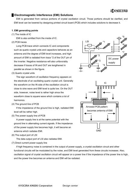
Electromagnetic Interference (EMI) Solutions - Kyocera
Electromagnetic Interference (EMI) Solutions - Kyocera
Electromagnetic Interference (EMI) Solutions - Kyocera

You also want an ePaper? Increase the reach of your titles
YUMPU automatically turns print PDFs into web optimized ePapers that Google loves.
█ <strong>Electromagnetic</strong> <strong>Interference</strong> (<strong>EMI</strong>) <strong>Solutions</strong><br />
<strong>EMI</strong> is generated from various portions of crystal oscillation circuit. Those portions should be clarified, and<br />
<strong>EMI</strong> level can be lowered by designing printed circuit board (PCB) which includes solutions to decrease it.<br />
1. <strong>EMI</strong> generating points<br />
(1) The inside of IC<br />
<strong>EMI</strong> is also emitted from the inside of IC.<br />
(2) PCB traces<br />
Long PCB trace which connects IC and components<br />
such as quartz crystal units and capacitors behaves as an<br />
antenna and the degree of <strong>EMI</strong> level increases, and high<br />
amount of <strong>EMI</strong> is radiated from trace *2 of the OUT pin of<br />
the inverter. Negative resistance will also unfavorably<br />
decrease if traces of IN and OUT are lengthened in<br />
parallel as shown in the figure.<br />
(3) Quartz crystal units<br />
The sign waveform of oscillation frequency appears on<br />
the electrode of an oscillating quartz crystal unit. Generally<br />
the waveform on the IN side of the oscillation circuit is<br />
close to sine wave and <strong>EMI</strong> level is quite low. On the OUT<br />
side, however, noise level is rather high since the<br />
waveform close to square wave which contains a lot of<br />
harmonics.<br />
(4) The ground line of PCB<br />
If the impedance of the ground line is high, radiated <strong>EMI</strong><br />
level will be rather high.<br />
(5) The power supply line of PCB<br />
A power supply line is at the same potential with the<br />
ground line in alternating current signals. If the impedance<br />
of the power supply line becomes high, it will become an<br />
antenna which radiates <strong>EMI</strong>.<br />
(6) The output port of LSI<br />
The data output port of LSI also radiates <strong>EMI</strong>.<br />
(7) Direct current power supply line<br />
KYOCERA KINSEKI Corporation Design center<br />
LSI<br />
*2<br />
*3<br />
*1<br />
*4<br />
IC<br />
Arrowed PCB pattern<br />
DC power<br />
supply<br />
becomes antenna of <strong>EMI</strong><br />
If high frequency noise is contained in the output of power supply, a crystal oscillation circuit and other<br />
functional circuits will be modulated by the noise, and <strong>EMI</strong> level generated from these circuits increases. Also,<br />
oscillation signal of crystal oscillation circuit will appear on a power line if the impedance of the power line is high,<br />
and the power line becomes an antenna and <strong>EMI</strong> will be radiated.<br />
GND<br />
*5<br />
*6<br />
*7
2. <strong>EMI</strong> <strong>Solutions</strong><br />
Since the oscillation waveform on the IN side of the Pierce crystal oscillation circuit using a C-MOS inverter<br />
exhibits a waveform similar or equal to sign wave, harmonics generated from this portion are minimal. On the<br />
other hand, the waveform on the OUT side of the inverter is square or distorted square wave, it contains a lot of<br />
harmonics. PCB trace connected to this portion becomes an antenna, and radiates <strong>EMI</strong>.<br />
(1) <strong>EMI</strong> solution for the noise generated from the inside of LSI<br />
By designing a field ground under LSI, it is possible to<br />
decrease <strong>EMI</strong> radiated under LSI.<br />
(2) <strong>EMI</strong> generated from PCB traces<br />
As shown in the figure, PCB should be designed with<br />
the shortest trace length so that the trace connecting<br />
components such as a crystal unit and capacitors with LSI<br />
does not become an antenna which radiates <strong>EMI</strong>.<br />
Furthermore, it is also effective to shield the signal pattern<br />
area of oscillation circuit with a ground pattern. However,<br />
one should be careful upon designing PCB, since negative<br />
resistance will decrease if these traces are routed too<br />
close. Also, it is important to design ground pattern not to<br />
make a loop by leaving the trace end open.<br />
KYOCERA KINSEKI Corporation Design center<br />
Top view<br />
LSI Ground pattern<br />
Side view<br />
"Open" end without making a loop.<br />
IC<br />
GND<br />
The pattern of OUT terminal needs to<br />
be designed the shortest.<br />
Since high amount of <strong>EMI</strong> is radiated from the line connected to the OUT terminal of the inverter oscillation<br />
part, it is important to design this pattern length shortest. The waveform of the IN terminal of the inverter is a<br />
sign wave in most cases, the level of <strong>EMI</strong> is low. The increases of <strong>EMI</strong> arising by PCB pattern of the OUT<br />
terminal becoming longer than the pattern of the IN terminal is much less compared with the case when the<br />
pattern of the OUT terminal is lengthened.<br />
Please refer to " Precautions on PCB design".<br />
(3) <strong>EMI</strong> radiated from quartz crystal units<br />
In SMD crystal units with metal cap (CX-2520SB,<br />
CX-3225SB, KSX-23, CX-4025S, CX-96F, KSX-35,<br />
KSX-36, CX-91F), <strong>EMI</strong> level radiated from the cap of a<br />
crystal unit can be decreased, if these terminals are<br />
connected to ground since #2 and #4 terminals are<br />
internally connected to the metal cap.<br />
To oscillation circuit<br />
GND<br />
X-tal<br />
Top view<br />
As for the leaded type quartz crystal units, oscillation signal appears in a metal case, and they are radiated as<br />
<strong>EMI</strong>.<br />
Please use crystal unit "CX-49L" equipped with a metal jacket to connect a metal case to ground decreasing<br />
radiated <strong>EMI</strong> level.<br />
(4) <strong>EMI</strong> radiated from the ground line<br />
If the layout of the ground pattern on the capacitor end is long and thin, it will become an antenna for the<br />
portion radiating <strong>EMI</strong>, and PCB needs to be designed so that they should be connected to the ground line with<br />
the shortest length. Please refer to (2) on the above.<br />
GND<br />
PCB
(5) <strong>EMI</strong> radiated from the power supply line<br />
It is effective to insert bypass capacitors with several<br />
values of different self-resonance frequencies so that the<br />
impedance of a power supply line shall not become high in<br />
wide frequency range. Usually, bypass capacitors are<br />
connected with the shortest length closest to the power<br />
supply terminal of LSI as shown in the right hand side<br />
figure. It is very effective to insert these capacitors in<br />
several places in PCB with long power supply line.<br />
KYOCERA KINSEKI Corporation Design center<br />
Power supply line<br />
All capacitors are placed closest to<br />
the LSI with the shortest pattern.<br />
1.0 0.1 0.01<br />
0.001 micro F<br />
A bypass capacitor is required for each power supply line when LSI needs several power supply voltages.<br />
Large value capacitors such as several micro farads are usually used for low frequency noise, but the care<br />
should be taken since regulator IC itself may oscillate if capacitors with large values are connected to the output<br />
terminal of regulator IC. Furthermore, it is effective to use <strong>EMI</strong> filters to suppress <strong>EMI</strong> radiated from the power<br />
supply line.<br />
(6) <strong>EMI</strong> radiated from the data output port<br />
Line filters may be used depending on the form of data. If it is not possible, it is effective to shield the area of<br />
data transmission line, and shield the other side of PCB by the ground pattern. Unused ports should be<br />
terminated with adequate impedance indicated in the LSI manual.<br />
(7) <strong>EMI</strong> radiated from the power supply unit<br />
In order to lessen <strong>EMI</strong> radiated from a direct-current power supply circuit, it is effective to shield the circuit with<br />
a metal cover or equivalent.<br />
3. Oscillation circuit structure and selection of circuit constants to decrease <strong>EMI</strong>.<br />
(Measure to lessen harmonics)<br />
The amount and level of <strong>EMI</strong> change depending on oscillation waveforms, and <strong>EMI</strong> decreases the most with<br />
sine wave. Since the oscillation waveform of the IN terminal of the inverter is close to sign wave, harmonics<br />
generated from this terminal are little in the C-MOS inverter crystal oscillation circuit. However, square wave of<br />
the OUT terminal which the sign wave of the IN terminal is amplified contains many harmonics. It is possible to<br />
decrease the distortion of the oscillation waveform of the OUT terminal and to decrease <strong>EMI</strong> by the following<br />
method.<br />
(1) Decrease the amount of the quantity of the electric charge which is charged and discharged in C2 using Rd<br />
and Rx. It is necessary to check that it satisfies the target value of design by circuit examination while selecting<br />
proper resistance values, since negative resistance of oscillation circuit decreases and oscillation starting time<br />
becomes long.<br />
(2) Use extremely small value compared with C1 and C2.<br />
If the capacitance of the OUT side is made small<br />
compared with the IN side, values such as C1=22pF and<br />
C2=5pF for example, the distortion of the waveform of<br />
the OUT terminal and <strong>EMI</strong> level will decrease. However,<br />
if the capacitance of the OUT side is made excessively<br />
small, the amplitude level will become low, and it is<br />
necessary to confirm that the OUT level is sufficient to<br />
drive the circuit of the following stage.<br />
LSI<br />
X-tal Rd<br />
Sine wave Rx Square wave or<br />
C1<br />
Rf =1M ohm<br />
C2<br />
sine wave<br />
with distortion