Electromagnetic Interference (EMI) Solutions - Kyocera
Electromagnetic Interference (EMI) Solutions - Kyocera
Electromagnetic Interference (EMI) Solutions - Kyocera

Create successful ePaper yourself
Turn your PDF publications into a flip-book with our unique Google optimized e-Paper software.
2. <strong>EMI</strong> <strong>Solutions</strong><br />
Since the oscillation waveform on the IN side of the Pierce crystal oscillation circuit using a C-MOS inverter<br />
exhibits a waveform similar or equal to sign wave, harmonics generated from this portion are minimal. On the<br />
other hand, the waveform on the OUT side of the inverter is square or distorted square wave, it contains a lot of<br />
harmonics. PCB trace connected to this portion becomes an antenna, and radiates <strong>EMI</strong>.<br />
(1) <strong>EMI</strong> solution for the noise generated from the inside of LSI<br />
By designing a field ground under LSI, it is possible to<br />
decrease <strong>EMI</strong> radiated under LSI.<br />
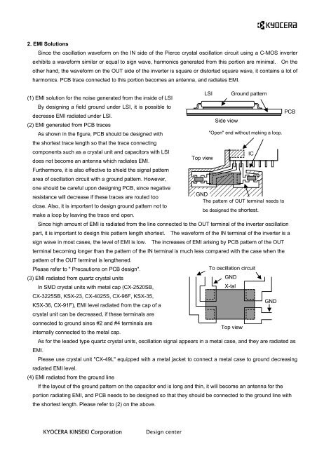
(2) <strong>EMI</strong> generated from PCB traces<br />
As shown in the figure, PCB should be designed with<br />
the shortest trace length so that the trace connecting<br />
components such as a crystal unit and capacitors with LSI<br />
does not become an antenna which radiates <strong>EMI</strong>.<br />
Furthermore, it is also effective to shield the signal pattern<br />
area of oscillation circuit with a ground pattern. However,<br />
one should be careful upon designing PCB, since negative<br />
resistance will decrease if these traces are routed too<br />
close. Also, it is important to design ground pattern not to<br />
make a loop by leaving the trace end open.<br />
KYOCERA KINSEKI Corporation Design center<br />
Top view<br />
LSI Ground pattern<br />
Side view<br />
"Open" end without making a loop.<br />
IC<br />
GND<br />
The pattern of OUT terminal needs to<br />
be designed the shortest.<br />
Since high amount of <strong>EMI</strong> is radiated from the line connected to the OUT terminal of the inverter oscillation<br />
part, it is important to design this pattern length shortest. The waveform of the IN terminal of the inverter is a<br />
sign wave in most cases, the level of <strong>EMI</strong> is low. The increases of <strong>EMI</strong> arising by PCB pattern of the OUT<br />
terminal becoming longer than the pattern of the IN terminal is much less compared with the case when the<br />
pattern of the OUT terminal is lengthened.<br />
Please refer to " Precautions on PCB design".<br />
(3) <strong>EMI</strong> radiated from quartz crystal units<br />
In SMD crystal units with metal cap (CX-2520SB,<br />
CX-3225SB, KSX-23, CX-4025S, CX-96F, KSX-35,<br />
KSX-36, CX-91F), <strong>EMI</strong> level radiated from the cap of a<br />
crystal unit can be decreased, if these terminals are<br />
connected to ground since #2 and #4 terminals are<br />
internally connected to the metal cap.<br />
To oscillation circuit<br />
GND<br />
X-tal<br />
Top view<br />
As for the leaded type quartz crystal units, oscillation signal appears in a metal case, and they are radiated as<br />
<strong>EMI</strong>.<br />
Please use crystal unit "CX-49L" equipped with a metal jacket to connect a metal case to ground decreasing<br />
radiated <strong>EMI</strong> level.<br />
(4) <strong>EMI</strong> radiated from the ground line<br />
If the layout of the ground pattern on the capacitor end is long and thin, it will become an antenna for the<br />
portion radiating <strong>EMI</strong>, and PCB needs to be designed so that they should be connected to the ground line with<br />
the shortest length. Please refer to (2) on the above.<br />
GND<br />
PCB