MPC107 PCI Bridge/Memory Controller Technical Summary
MPC107 PCI Bridge/Memory Controller Technical Summary
MPC107 PCI Bridge/Memory Controller Technical Summary
You also want an ePaper? Increase the reach of your titles
YUMPU automatically turns print PDFs into web optimized ePapers that Google loves.
Freescale Semiconductor, Inc...<br />
Semiconductor Products Sector<br />
Advance Information<br />
<strong>MPC107</strong> <strong>PCI</strong> <strong>Bridge</strong>/<strong>Memory</strong> <strong>Controller</strong><br />
<strong>Technical</strong> <strong>Summary</strong><br />
This document contains information on a new product under development by Motorola.<br />
Motorola reserves the right to change or discontinue this product without notice.<br />
© Motorola, Inc., 1999. All rights reserved.<br />
Freescale Semiconductor, Inc.<br />
Order Number: <strong>MPC107</strong>TS/D<br />
Rev. 0, 9/1999<br />
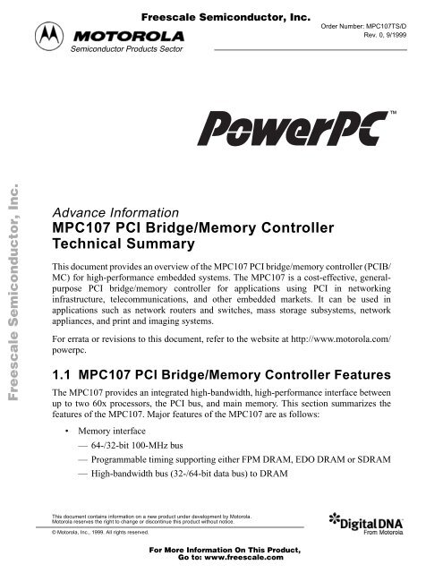
This document provides an overview of the <strong>MPC107</strong> <strong>PCI</strong> bridge/memory controller (<strong>PCI</strong>B/<br />
MC) for high-performance embedded systems. The <strong>MPC107</strong> is a cost-effective, generalpurpose<br />
<strong>PCI</strong> bridge/memory controller for applications using <strong>PCI</strong> in networking<br />
infrastructure, telecommunications, and other embedded markets. It can be used in<br />
applications such as network routers and switches, mass storage subsystems, network<br />
appliances, and print and imaging systems.<br />
For errata or revisions to this document, refer to the website at http://www.motorola.com/<br />
powerpc.<br />
1.1 <strong>MPC107</strong> <strong>PCI</strong> <strong>Bridge</strong>/<strong>Memory</strong> <strong>Controller</strong> Features<br />
The <strong>MPC107</strong> provides an integrated high-bandwidth, high-performance interface between<br />
up to two 60x processors, the <strong>PCI</strong> bus, and main memory. This section summarizes the<br />
features of the <strong>MPC107</strong>. Major features of the <strong>MPC107</strong> are as follows:<br />
• <strong>Memory</strong> interface<br />
— 64-/32-bit 100-MHz bus<br />
— Programmable timing supporting either FPM DRAM, EDO DRAM or SDRAM<br />
— High-bandwidth bus (32-/64-bit data bus) to DRAM<br />
For More Information On This Product,<br />
Go to: www.freescale.com
Freescale Semiconductor, Inc...<br />
<strong>MPC107</strong> <strong>PCI</strong> <strong>Bridge</strong>/<strong>Memory</strong> <strong>Controller</strong> Features<br />
2<br />
Freescale Semiconductor, Inc.<br />
— Supports one to eight banks of 4-, 16-, 64-, or 128-Mbit memory devices, and up<br />
to four banks of 256-Mbit SDRAM devices<br />
— Supports 1-Mbyte to 1-Gbyte DRAM memory<br />
— 144 Mbytes of ROM space<br />
— 8-, 32-, or 64-bit ROM<br />
— Write buffering for <strong>PCI</strong> and processor accesses<br />
— Supports normal parity, read-modify-write (RMW), or ECC<br />
— Data-path buffering between memory interface and processor<br />
— Low-voltage TTL logic (LVTTL) interfaces<br />
— Port X: 8-, 32-, or 64-bit general-purpose I/O port using ROM controller<br />
interface with programmable address strobe timing<br />
• 32-bit <strong>PCI</strong> interface operating up to 66 MHz<br />
— <strong>PCI</strong> 2.1-compliant<br />
— <strong>PCI</strong> 5.0-V tolerance<br />
— Support for <strong>PCI</strong> locked accesses to memory<br />
— Support for accesses to <strong>PCI</strong> memory, I/O, and configuration spaces<br />
— Selectable big- or little-endian operation<br />
— Store gathering of processor-to-<strong>PCI</strong> write and <strong>PCI</strong>-to-memory write accesses<br />
— <strong>Memory</strong> prefetching of <strong>PCI</strong> read accesses<br />
— Selectable hardware-enforced coherency<br />
— <strong>PCI</strong> bus arbitration unit (five request/grant pairs)<br />
— <strong>PCI</strong> agent mode capability<br />
— Address translation unit<br />
— Some internal configuration registers accessible from <strong>PCI</strong><br />
• Two-channel integrated DMA controller (writes to ROM/Port X not supported)<br />
— Supports direct mode or chaining mode (automatic linking of DMA transfers)<br />
— Supports scatter gathering—read or write discontinuous memory<br />
— Interrupt on completed segment, chain, and error<br />
— Local-to-local memory<br />
— <strong>PCI</strong>-to-<strong>PCI</strong> memory<br />
— <strong>PCI</strong>-to-local memory<br />
— <strong>PCI</strong> memory-to-local memory<br />
<strong>MPC107</strong> <strong>PCI</strong> <strong>Bridge</strong>/<strong>Memory</strong> <strong>Controller</strong> <strong>Technical</strong> <strong>Summary</strong><br />
For More Information On This Product,<br />
Go to: www.freescale.com
Freescale Semiconductor, Inc...<br />
<strong>MPC107</strong> <strong>PCI</strong> <strong>Bridge</strong>/<strong>Memory</strong> <strong>Controller</strong> <strong>Technical</strong> <strong>Summary</strong><br />
For More Information On This Product,<br />
Go to: www.freescale.com<br />
<strong>MPC107</strong> <strong>PCI</strong>/MC Applications<br />
• Message unit<br />
— Two doorbell registers<br />
— An extended doorbell register mechanism that facilitates interprocessor<br />
communication through interrupts in a dual-local-processor system<br />
— Two inbound and two outbound messaging registers<br />
—I<br />
2<br />
O message controller<br />
Freescale Semiconductor, Inc.<br />
• I2C<br />
controller with full master/slave support (except broadcast all)<br />
• Embedded programmable interrupt controller (EPIC)<br />
— Five hardware interrupts (IRQs) or 16 serial interrupts<br />
— Four programmable timers<br />
• Integrated <strong>PCI</strong> bus, CPU, and SDRAM clock generation<br />
• Programmable <strong>PCI</strong> bus, 60x, and memory interface output drivers<br />
• Dynamic power management—Supports 60x nap, doze, sleep, and suspend modes<br />
• Programmable input and output signals with watchpoint capability<br />
• Built-in <strong>PCI</strong> bus performance monitor facility<br />
• Debug features<br />
— Error injection/capture on data path<br />
— IEEE 1149.1 (JTAG)/test interface<br />
• Processor interface<br />
— Supports up to two PowerPC microprocessors with 60x bus interface<br />
— Supports various operating frequencies and bus divider ratios<br />
— 32-bit address bus, 64/32-bit data bus supported at 100 MHz<br />
— Supports full memory coherency<br />
— Supports optional local bus slave<br />
— Decoupled address and data buses for pipelining of 60x accesses<br />
— Store gathering on 60x-to-<strong>PCI</strong> writes<br />
— Concurrent transactions on 60x and <strong>PCI</strong> buses supported<br />
1.2 <strong>MPC107</strong> <strong>PCI</strong>/MC Applications<br />
The <strong>MPC107</strong> can be used in either a system host configuration or as a peripheral device.<br />
For system applications where cost, space, and power consumption are critical parameters,<br />
yet performance cannot be sacrificed, the <strong>MPC107</strong> provides a complete solution. The<br />
<strong>MPC107</strong> is shown in Figure 1-1 as a host bridge.<br />
3
Freescale Semiconductor, Inc...<br />
<strong>MPC107</strong> <strong>PCI</strong>/MC Applications<br />
4<br />
<strong>MPC107</strong><br />
DMA<br />
PowerPC<br />
Microprocessor<br />
MU(I 2O)<br />
I 2 C<br />
EPIC<br />
<strong>PCI</strong> Bus<br />
Peripheral<br />
Logic<br />
ROM /<br />
Port X<br />
Figure 1-1. System Using <strong>MPC107</strong> as a Host <strong>Bridge</strong><br />
With the embedded enhancements provided in the <strong>MPC107</strong>, it is possible to use it in<br />
distributed I/O processor applications as shown in Figure 1-2.<br />
Periph. 2<br />
<strong>MPC107</strong><br />
DMA<br />
I 2 C<br />
EPIC<br />
Freescale Semiconductor, Inc.<br />
<strong>PCI</strong> Bus<br />
MU(I 2O)<br />
CTRL<br />
up to 66 MHz<br />
Data<br />
Peripheral Peripheral Peripheral <strong>PCI</strong> to <strong>PCI</strong><br />
1 2 3 <strong>Bridge</strong><br />
Peripheral<br />
Logic<br />
PowerPC<br />
Microprocessor<br />
Host Processor<br />
Host <strong>Bridge</strong><br />
CTRL<br />
Data<br />
<strong>PCI</strong> Bus<br />
Host <strong>Memory</strong><br />
up to 66 MHz<br />
Local <strong>Memory</strong>:<br />
DRAM, EDO,<br />
SDRAM<br />
Figure 1-2. Embedded System Using the <strong>MPC107</strong> as a <strong>Bridge</strong> to a<br />
Distributed I/O Processor<br />
<strong>MPC107</strong> <strong>PCI</strong> <strong>Bridge</strong>/<strong>Memory</strong> <strong>Controller</strong> <strong>Technical</strong> <strong>Summary</strong><br />
For More Information On This Product,<br />
Go to: www.freescale.com<br />
Local <strong>Memory</strong>:<br />
DRAM, EDO,<br />
SDRAM<br />
Peripheral Peripheral<br />
System I/O <strong>PCI</strong> to <strong>PCI</strong><br />
1 3<br />
<strong>Controller</strong> <strong>Bridge</strong><br />
ROM /<br />
Port X<br />
<strong>PCI</strong> Bus
Freescale Semiconductor, Inc...<br />
<strong>MPC107</strong> <strong>PCI</strong> <strong>Bridge</strong>/<strong>Memory</strong> <strong>Controller</strong> <strong>Technical</strong> <strong>Summary</strong><br />
For More Information On This Product,<br />
Go to: www.freescale.com<br />
<strong>MPC107</strong> <strong>PCI</strong>/MC Applications<br />
The <strong>MPC107</strong> can also be used with a peripheral processing device as shown in Figure 1-3.<br />
In this case, the <strong>PCI</strong>-to-<strong>PCI</strong> bridge shown Figure 1-3 could be of the <strong>PCI</strong> type 0 variety. The<br />
<strong>MPC107</strong> would not be part of the system configuration map. This configuration is useful in<br />
applications such as RAID controllers or multi-port network controllers where the I/O<br />
devices shown are SCSI controllers or Ethernet controllers, respectively.<br />
<strong>PCI</strong> Bus<br />
Host Processor<br />
Host <strong>Bridge</strong><br />
up to 66 MHz<br />
CTRL<br />
Host <strong>Memory</strong><br />
Peripheral<br />
Peripheral<br />
<strong>PCI</strong>-to-<strong>PCI</strong> I/O Device I/O Device Peripheral<br />
1<br />
2<br />
<strong>Bridge</strong><br />
3<br />
Local <strong>PCI</strong> Bus<br />
<strong>MPC107</strong><br />
DMA<br />
MU(I 2 O)<br />
I 2 C<br />
EPIC<br />
Peripheral<br />
Logic<br />
PowerPC<br />
Microprocessor<br />
Freescale Semiconductor, Inc.<br />
ROM /<br />
Port X<br />
Local <strong>Memory</strong>:<br />
DRAM, EDO,<br />
SDRAM<br />
Figure 1-3. Embedded System Using <strong>MPC107</strong> with a Peripheral Processor<br />
The processor bus interface (60x) of the <strong>MPC107</strong> contains all of the necessary arbitration<br />
and control logic to communicate with up to two PowerPC microprocessors in a symmetric<br />
multiprocessing environment. In addition, the <strong>MPC107</strong> also has a side-band mode to allow<br />
an alternate bus slave to capture address tenures. This application is show in Figure 1-4.<br />
Data<br />
System I/O<br />
<strong>Controller</strong><br />
5
Freescale Semiconductor, Inc...<br />
<strong>MPC107</strong> Major Functional Blocks<br />
6<br />
Local Bus<br />
Slave<br />
60x Bus<br />
Freescale Semiconductor, Inc.<br />
PowerPC<br />
Microprocessor<br />
<strong>MPC107</strong><br />
I 2 DMA<br />
MU(I2O) C<br />
EPIC<br />
<strong>PCI</strong> Bus<br />
Peripheral<br />
Logic<br />
PowerPC<br />
Microprocessor<br />
ROM /<br />
Port X<br />
Figure 1-4. Multiprocessor System Using the <strong>MPC107</strong> and a Local Bus Slave<br />
1.3 <strong>MPC107</strong> Major Functional Blocks<br />
The <strong>MPC107</strong> integrates a <strong>PCI</strong> bridge, memory controller, DMA controller, EPIC interrupt<br />
controller/timers, a message unit with an Intelligent Input/Output (I2O)<br />
message controller,<br />
and an Inter-Integrated Circuit (I2<br />
C) controller. The integration reduces the overall<br />
packaging requirements and the number of discrete devices required for an embedded<br />
system.<br />
Figure 1-5 shows the major functional units within the <strong>MPC107</strong>. Note that this is a<br />
conceptual block diagram intended to show the basic features rather than an attempt to<br />
show how these features are physically implemented.<br />
CTRL<br />
Data<br />
<strong>MPC107</strong> <strong>PCI</strong> <strong>Bridge</strong>/<strong>Memory</strong> <strong>Controller</strong> <strong>Technical</strong> <strong>Summary</strong><br />
For More Information On This Product,<br />
Go to: www.freescale.com<br />
Local <strong>Memory</strong>:<br />
DRAM, EDO,<br />
SDRAM
Freescale Semiconductor, Inc...<br />
I 2 C<br />
5 IRQs/<br />
16 Serial<br />
Interrupts<br />
<strong>MPC107</strong><br />
Message<br />
Unit<br />
(with I 2 O)<br />
DMA<br />
<strong>Controller</strong><br />
I 2 C<br />
<strong>Controller</strong><br />
EPIC<br />
Interrupt<br />
<strong>Controller</strong><br />
/Timers<br />
60x Bus Interface (64- or 32-Bit Data Bus)<br />
Central<br />
Control<br />
Unit<br />
<strong>PCI</strong> Bus<br />
Interface Unit<br />
Address<br />
Translator<br />
32-Bit<br />
<strong>PCI</strong> Interface<br />
<strong>PCI</strong><br />
Arbiter<br />
1.3.1 60x Processor Interface<br />
Freescale Semiconductor, Inc.<br />
Peripheral Logic Block<br />
Address<br />
(32-Bit)<br />
Data (64-Bit)<br />
Configuration<br />
Registers<br />
Five<br />
Request/Grant<br />
Pairs<br />
Data Path<br />
ECC <strong>Controller</strong><br />
<strong>Memory</strong><br />
<strong>Controller</strong><br />
Figure 1-5. <strong>MPC107</strong> Block Diagram<br />
<strong>MPC107</strong> <strong>PCI</strong> <strong>Bridge</strong>/<strong>Memory</strong> <strong>Controller</strong> <strong>Technical</strong> <strong>Summary</strong><br />
For More Information On This Product,<br />
Go to: www.freescale.com<br />
<strong>MPC107</strong> Major Functional Blocks<br />
The <strong>MPC107</strong> supports a programmable interface to a variety of PowerPC microprocessors<br />
operating at select bus speeds. The 60x address bus is 32 bits wide and the data bus is<br />
configurable to be 64 or 32 bits wide. The 60x processor interface of the <strong>MPC107</strong> uses a<br />
subset of the 60x bus protocol, supporting single-beat and burst data transfers. The address<br />
and data buses are decoupled to support pipelined transactions.<br />
In this document, the term ‘60x’ is used to denote a 32-bit microprocessor from the<br />
PowerPC architecture family that conforms to the bus interface of the MPC603e, MPC740,<br />
MPC750, or MPC7400 microprocessors. 60x processors implement the PowerPC<br />
architecture as it is specified for 32-bit addressing, which provides 32-bit effective (logical)<br />
addresses, integer data types of 8, 16, and 32 bits, and floating-point data types of 32 and<br />
64 bits (single-precision and double-precision).<br />
Two signals on the <strong>MPC107</strong>, local bus slave claim (LBCLAIM) and data bus grant local<br />
bus slave (DBGLB), are provided for an optional local bus slave. However, the local bus<br />
slave must be capable of generating the transfer acknowledge (TA) signal to interact with<br />
the 60x processor(s).<br />
DLL<br />
PLL<br />
Fanout<br />
Buffers<br />
OSC_IN<br />
Additional features:<br />
• Programmable I/O<br />
• with Watchpoint<br />
• JTAG/COP Interface<br />
• Power Management<br />
Data Bus<br />
(64- or 32-bit)<br />
with 8-bit Parity<br />
or ECC<br />
<strong>Memory</strong>/ROM/<br />
Port X Control/<br />
Address<br />
SDRAM_SYNC_IN<br />
SDRAM Clocks<br />
CPU Clocks<br />
<strong>PCI</strong>_SYNC_IN<br />
<strong>PCI</strong> Bus<br />
Clocks<br />
7
Freescale Semiconductor, Inc...<br />
<strong>MPC107</strong> Major Functional Blocks<br />
Depending on the system implementation, the processor bus may operate at the <strong>PCI</strong> bus<br />
clock rate, or at a multiple of the <strong>PCI</strong> bus clock rate (determined at reset). The 60x processor<br />
bus is synchronous, with all timing relative to the rising edge of the 60x bus clock.<br />
When two 60x processors are used, the two sets of bus request, bus grant, and data bus grant<br />
signals allow for arbitration between the 60x processors. The 60x processors share all 60x<br />
interface signals of the <strong>MPC107</strong>, except the bus arbitration signals.<br />
1.3.2 <strong>Memory</strong> System Interface<br />
The <strong>MPC107</strong> memory interface controls processor and <strong>PCI</strong> interactions to main memory.<br />
It supports a variety of DRAM, and flash or ROM configurations as main memory. The<br />
<strong>MPC107</strong> supports fast page mode (FPM), extended data out (EDO) and synchronous<br />
DRAM (SDRAM). The maximum supported memory size is 1 Gbyte of DRAM or<br />
SDRAM and 144 Mbytes of ROM/flash. SDRAM must comply with the JEDEC SDRAM<br />
specification.<br />
The <strong>MPC107</strong> implements Port X, a memory bus interface that facilitates the connection of<br />
general-purpose I/O devices. The Port X functionality allows the designer to connect<br />
external registers, communication devices, and other such devices directly to the <strong>MPC107</strong>.<br />
Some devices may require a small amount of external logic to properly generate address<br />
strobes, chip selects, and other signals.<br />
The <strong>MPC107</strong> is designed to control a 32-bit or 64-bit data path to main memory DRAM or<br />
SDRAM. For a 32-bit data path, the <strong>MPC107</strong> can be configured to check and generate byte<br />
parity using four parity bits. For a 64-bit data path, the <strong>MPC107</strong> can be configured to<br />
support parity or ECC checking and generation with eight parity/syndrome bits checked<br />
and generated. Note that the data bus width (32- or 64-bit) chosen at reset for the 60x bus<br />
interface is also used for the memory interface.<br />
The <strong>MPC107</strong> supports DRAM bank sizes from 1 to 128 Mbytes, SDRAM bank sizes of 1<br />
to 256 Mbytes, and provides bank start address and end address configuration registers.<br />
Note that the <strong>MPC107</strong> does not support mixed DRAM/SDRAM configurations. The<br />
<strong>MPC107</strong> can be configured so that appropriate row and column address multiplexing<br />
occurs according to the accessed memory bank. Addresses are provided to DRAM and<br />
SDRAM through a 13-bit interface for DRAM and a 15-bit interface for SDRAM.<br />
The memory bus width is configured at reset as 32- or 64-bits wide, depending on the<br />
setting of the MDL0 reset configuration signal. Four chip selects, one write enable, one<br />
output enable, and up to 21 address signals are provided for ROM/flash systems.<br />
1.3.3 Peripheral Component Interconnect (<strong>PCI</strong>) Interface<br />
The <strong>PCI</strong> interface for the <strong>MPC107</strong> is compliant with the Peripheral Component<br />
Interconnect Specification Revision 2.1. The <strong>PCI</strong> interface provides mode-selectable, bigto<br />
little-endian conversion. The <strong>MPC107</strong> provides an interface to the <strong>PCI</strong> bus running at<br />
speeds up to 66 MHz.<br />
8<br />
Freescale Semiconductor, Inc.<br />
<strong>MPC107</strong> <strong>PCI</strong> <strong>Bridge</strong>/<strong>Memory</strong> <strong>Controller</strong> <strong>Technical</strong> <strong>Summary</strong><br />
For More Information On This Product,<br />
Go to: www.freescale.com
Freescale Semiconductor, Inc...<br />
<strong>MPC107</strong> <strong>PCI</strong> <strong>Bridge</strong>/<strong>Memory</strong> <strong>Controller</strong> <strong>Technical</strong> <strong>Summary</strong><br />
For More Information On This Product,<br />
Go to: www.freescale.com<br />
<strong>MPC107</strong> Major Functional Blocks<br />
The <strong>MPC107</strong>’s <strong>PCI</strong> interface can be configured as host or agent. In host mode, the interface<br />
acts as the main memory controller for the system and responds to all host memory<br />
transactions.<br />
In agent mode, the <strong>MPC107</strong> can be configured to respond to a programmed window of <strong>PCI</strong><br />
memory space. A variety of initialization modes are provided to boot the device.<br />
1.3.3.1 <strong>PCI</strong> Bus Arbitration Unit<br />
The <strong>MPC107</strong> contains a <strong>PCI</strong> bus arbitration unit, which eliminates the need for an external<br />
unit, thus lowering system complexity and cost. It has the following features:<br />
• Five external arbitration signal pairs. The <strong>MPC107</strong> is the sixth member of the<br />
arbitration pool.<br />
• The bus arbitration unit allows fairness as well as a priority mechanism.<br />
• A two-level round-robin scheme is used in which each device can be programmed<br />
within a pool of a high- or low-priority arbitration. One member of the low-priority<br />
pool is promoted to the high-priority pool. As soon as it is granted the bus, it returns<br />
to the low-priority pool.<br />
• The unit can be disabled to allow a remote arbitration unit to be used.<br />
1.3.3.2 Address Maps and Translation<br />
The <strong>MPC107</strong>’s processor bus interface supports memory-mapped accesses. The address<br />
space is divided between memory and <strong>PCI</strong> according to one of two allowable address<br />
maps—map A and map B. Note that the support of map A is provided for backward<br />
compatibility only. It is strongly recommended that new designs use map B because map A<br />
may not be supported in future devices.<br />
An inbound and outbound <strong>PCI</strong> address translation mechanism is provided to support the<br />
use of the <strong>MPC107</strong> in agent mode. Note that address translation is supported only for agent<br />
mode; it is not supported when the <strong>MPC107</strong> is operating in host mode. Also note that since<br />
agent mode is supported only for address map B, address translation is supported only for<br />
address map B.<br />
When the <strong>MPC107</strong> is configured to be a <strong>PCI</strong> agent, the amount of local memory visible to<br />
the system is programmable. In addition, it may be necessary to map the local memory to<br />
a different system memory address space. The address translation unit handles the mapping<br />
of both inbound and outbound transactions for these cases.<br />
1.3.3.3 Byte Ordering<br />
Freescale Semiconductor, Inc.<br />
The <strong>MPC107</strong> allows the processor to run in either big- or little-endian mode (except for the<br />
initial boot code which must run in big-endian mode).<br />
9
Freescale Semiconductor, Inc...<br />
<strong>MPC107</strong> Major Functional Blocks<br />
1.3.3.4 <strong>PCI</strong> Agent Capability<br />
In certain applications, the embedded system architecture dictates that the <strong>MPC107</strong> bridges<br />
to a peripheral processor. In this case, the peripheral logic must not act like a host bridge<br />
for the <strong>PCI</strong> bus. Instead it functions as a configurable device that is accessed by a host<br />
bridge. This capability allows multiple <strong>MPC107</strong> devices to coexist with other <strong>PCI</strong><br />
peripheral devices on a single <strong>PCI</strong> bus. The <strong>MPC107</strong> has <strong>PCI</strong> 2.1- compliant configuration<br />
capabilities.<br />
1.3.4 DMA <strong>Controller</strong><br />
The integrated DMA controller contains two independent units. Note that the DMA writing<br />
capability for local memory is available for DRAM and SDRAM, but writing is not<br />
available for the ROM/Port X interface. Each DMA unit is capable of performing the<br />
following types of transfers:<br />
• <strong>PCI</strong>-to-local memory<br />
• Local-to-<strong>PCI</strong> memory<br />
• <strong>PCI</strong>-to-<strong>PCI</strong> memory<br />
• Local-to-local memory<br />
The DMA controller allows chaining through local memory-mapped chain descriptors.<br />
Transfers can be scatter gathered and misaligned. Interrupts are provided on completed<br />
segment, chain, and error conditions.<br />
1.3.5 Message Unit (MU)<br />
Many embedded applications require handshake algorithms to pass control, status, and data<br />
information from one owner to another. This is made easier with doorbell and message<br />
registers. The <strong>MPC107</strong> has a message unit (MU) that implements doorbell and message<br />
registers as well as an I<br />
10<br />
2<br />
O interface. The MU has many conditions that can cause interrupts<br />
and uses the EPIC unit to signal interrupts to the <strong>PCI</strong> interface and interrupts to the<br />
processor.<br />
1.3.5.1 Doorbell Registers<br />
Freescale Semiconductor, Inc.<br />
The <strong>MPC107</strong> MU contains one 32-bit inbound doorbell register and one 32-bit outbound<br />
doorbell register. The inbound doorbell register allows a remote processor to set a bit in the<br />
register from the <strong>PCI</strong> bus. This, in turn, generates an interrupt to the local processor.<br />
The local processor can write to the outbound register, causing the outbound interrupt<br />
signal INTA to assert, thus interrupting the host processor. Once INTA is generated, it can<br />
be cleared only by the host processor by writing ones to the bits that are set in the outbound<br />
doorbell register.<br />
<strong>MPC107</strong> <strong>PCI</strong> <strong>Bridge</strong>/<strong>Memory</strong> <strong>Controller</strong> <strong>Technical</strong> <strong>Summary</strong><br />
For More Information On This Product,<br />
Go to: www.freescale.com
Freescale Semiconductor, Inc...<br />
Freescale Semiconductor, Inc.<br />
1.3.5.2 Extended Doorbell Register Facility<br />
<strong>MPC107</strong> <strong>PCI</strong> <strong>Bridge</strong>/<strong>Memory</strong> <strong>Controller</strong> <strong>Technical</strong> <strong>Summary</strong><br />
For More Information On This Product,<br />
Go to: www.freescale.com<br />
<strong>MPC107</strong> Major Functional Blocks<br />
The <strong>MPC107</strong> MU also contains an extended doorbell register mechanism that facilitates<br />
interprocessor communication through interrupts in a dual-local-processor system. For<br />
example, processor 0 can write to the EDBW1S register to generate an interrupt to<br />
processor 1. Processor 1 can then clear the interrupt by writing to the EDBW1C register.<br />
The same process can be used if processor 1 needs to interrupt processor 0. Use of this<br />
facility requires that the rest of the MU be disabled.<br />
1.3.5.3 Inbound and Outbound Message Registers<br />
The <strong>MPC107</strong> contains two 32-bit inbound message registers and two 32-bit outbound<br />
message registers. The inbound registers allow a remote host or <strong>PCI</strong> master to write a 32bit<br />
value, causing an interrupt to the local processor. The outbound registers allow the local<br />
processor to write an outbound message which causes the outbound interrupt signal INTA<br />
to assert.<br />
1.3.5.4 Intelligent Input/Output <strong>Controller</strong> (I2O)<br />
The intelligent I/O specification is an open standard that defines an abstraction layer<br />
interface between the OS and subsystem drivers. Messages are passed between the message<br />
abstraction layer from one device to another.<br />
The I2O<br />
specification describes a system as being made up of host processors and input/<br />
output platforms (IOPs). The host processor is a single processor or a collection of<br />
processors working together to execute a homogenous operating system. An IOP consists<br />
of a processor, memory, and I/O interfaces. The IOP functions separately from other<br />
processors within the system to handle system I/O functions.<br />
The I2O<br />
controller of the MU enhances communication between hosts and IOPs within a<br />
system. There are two paths for messages—an inbound queue is used to transfer messages<br />
from a remote host or IOP to the local processor, and an outbound queue is used to transfer<br />
messages from the local processor to the remote host. Each queue is implemented as a pair<br />
of FIFOs. The inbound and outbound message queues each consists of a free_list FIFO and<br />
a post_list FIFO.<br />
Messages are transferred between the host and the IOP using <strong>PCI</strong> memory-mapped<br />
registers. The <strong>MPC107</strong>’s I2O<br />
controller facilitates moving the messages to and from the<br />
inbound and outbound registers and local IOP memory. Interrupts signal the host and IOP<br />
to indicate the arrival of new messages.<br />
1.3.6 Inter-Integrated Circuit (I2C)<br />
<strong>Controller</strong><br />
2<br />
The I C serial interface has become an industry de facto standard for communicating with<br />
low-speed peripherals. Typically, it is used for system management functions and<br />
EEPROM support. The <strong>MPC107</strong> contains an I2<br />
C controller with full master and slave<br />
functionality.<br />
11
Freescale Semiconductor, Inc...<br />
<strong>MPC107</strong> Major Functional Blocks<br />
1.3.7 Embedded Programmable Interrupt <strong>Controller</strong> (EPIC)<br />
The integrated embedded programmable interrupt controller (EPIC) of the <strong>MPC107</strong><br />
reduces the overall component count in embedded applications. The EPIC unit is designed<br />
to collect external and internal hardware interrupts, prioritize them, and deliver them to the<br />
local processor.<br />
The module operates in one of three modes:<br />
• In direct mode, five level- or edge-triggered interrupts can be connected directly to<br />
an <strong>MPC107</strong>.<br />
• In pass-through mode, interrupts detected at the IRQ0 input are passed directly (with<br />
logic inversion) to the INT output signal. Also in this case, interrupts generated by<br />
the I2O,<br />
I2C,<br />
and DMA controllers are passed to the L_INT output signal.<br />
• The <strong>MPC107</strong> provides a serial delivery mechanism for when more than five external<br />
interrupt sources are needed. The serial mechanism allows for up to 16 interrupts to<br />
be serially scanned into the <strong>MPC107</strong>. This mechanism increases the number of<br />
interrupts without increasing the number of pins.<br />
The outbound interrupt request signal, L_INT, is used to signal interrupts to the host<br />
processor when the <strong>MPC107</strong> is configured for agent mode. The <strong>MPC107</strong> EPIC includes<br />
four programmable timers that can be used for system timing or for generating periodic<br />
interrupts.<br />
1.3.8 Integrated <strong>PCI</strong> Bus, CPU, and SDRAM Clock<br />
Generation<br />
There are two <strong>PCI</strong> bus clocking solutions directed towards different system requirements.<br />
For systems where the <strong>MPC107</strong> is the host controller with a minimum number of clock<br />
loads, five clock fanout buffers are provided on-chip.<br />
For systems requiring more clock fan out or where the <strong>MPC107</strong> is an agent device, external<br />
clock buffers may be used.<br />
The <strong>MPC107</strong> provides an on-chip delay-locked loop (DLL) that supplies the external<br />
memory bus clock signals to SDRAM banks and also supplies three CPU clock outputs that<br />
are synchronized to the SDRAM clocks. The memory bus clock signals are of the same<br />
frequency and synchronous with the processor clock signals.<br />
The four SDRAM clock outputs are generated by the internal DLL and can account for the<br />
trace length between SDRAM_SYNC_OUT signal and the SDRAM_SYNC_IN signal.<br />
The <strong>MPC107</strong> requires a single clock input signal, <strong>PCI</strong>_SYNC_IN, which can be driven by<br />
the <strong>PCI</strong> clock fan-out buffers—specifically the <strong>PCI</strong>_SYNC_OUT output. <strong>PCI</strong>_SYNC_IN<br />
can also be driven by an external clock driver.<br />
12<br />
Freescale Semiconductor, Inc.<br />
<strong>MPC107</strong> <strong>PCI</strong> <strong>Bridge</strong>/<strong>Memory</strong> <strong>Controller</strong> <strong>Technical</strong> <strong>Summary</strong><br />
For More Information On This Product,<br />
Go to: www.freescale.com
Freescale Semiconductor, Inc...<br />
<strong>MPC107</strong> <strong>PCI</strong> <strong>Bridge</strong>/<strong>Memory</strong> <strong>Controller</strong> <strong>Technical</strong> <strong>Summary</strong><br />
For More Information On This Product,<br />
Go to: www.freescale.com<br />
Power Management<br />
<strong>PCI</strong>_SYNC_IN is driven by the <strong>PCI</strong> bus frequency. An internal PLL, using <strong>PCI</strong>_SYNC_IN<br />
as a reference, generates an internal sys-logic-clk signal that is used for the internal logic.<br />
The processor (60x) bus clock frequency on the CPU_CLK[0:2] outputs is configured at<br />
reset (by the <strong>MPC107</strong> PLL configuration signals (PLL_CFG[0:3])) to be a multiple of the<br />
<strong>PCI</strong>_SYNC_IN frequency.<br />
1.4 Power Management<br />
The <strong>MPC107</strong> provides program-controllable power reduction modes for progressive<br />
reduction of power consumption and a system hardware mechanism for further power<br />
reduction.<br />
The <strong>MPC107</strong> provides hardware support for three levels of programmable power<br />
reduction—doze, nap, and sleep modes; each is invoked by programming configuration<br />
registers.<br />
The <strong>MPC107</strong> also has a fourth power reduction mode invoked by the assertion of the<br />
external SUSPEND signal. In suspend mode, the <strong>MPC107</strong> may have its clock input and<br />
PLL shut down for additional power savings. <strong>Memory</strong> refresh can be accomplished in two<br />
ways—either by using self-refresh mode DRAMs or by using the RTC input. To exit the<br />
suspend mode, the system clock must be turned on in sufficient time to restart the PLL.<br />
After this time, SUSPEND may be negated. In suspend mode, all bidirectional and output<br />
signals (except the memory refresh-related signals if RTC refresh is being used) are at high<br />
impedance and all input signals except the PLL_CFG[0:3] signals, HRST, and SUSPEND,<br />
are ignored. Note that the SUSPEND signal is monitored for negation during suspend<br />
mode.<br />
The <strong>MPC107</strong> is fully static, allowing internal logic states to be preserved during all powersaving<br />
modes.<br />
Table 1-1 summarizes the programmable power-saving modes for the <strong>MPC107</strong>.<br />
.<br />
PM<br />
Mode<br />
Full<br />
power<br />
Table 1-1. <strong>MPC107</strong> Power Modes <strong>Summary</strong><br />
Functioning Units Activation Method<br />
All units active — —<br />
Doze <strong>PCI</strong> address decoding and bus arbiter<br />
System RAM refreshing<br />
60x bus request and NMI monitoring<br />
EPIC unit<br />
I<br />
2C<br />
unit<br />
PLL<br />
Freescale Semiconductor, Inc.<br />
Controlled by software<br />
(write to PMCR1)<br />
Full-Power Wake Up<br />
Method<br />
<strong>PCI</strong> access to memory<br />
60x bus request<br />
Assertion of NMI<br />
1<br />
Hard Reset<br />
13
Freescale Semiconductor, Inc...<br />
Programmable I/O Signals with Watchpoint<br />
PM<br />
Mode<br />
Nap <strong>PCI</strong> address decoding and bus arbiter<br />
System RAM refreshing<br />
60x bus request and NMI monitoring<br />
EPIC unit<br />
I<br />
2C<br />
unit<br />
PLL<br />
Sleep <strong>PCI</strong> bus arbiter<br />
System RAM refreshing (can be disabled)<br />
60x bus request and NMI monitoring<br />
EPIC unit<br />
2<br />
I C unit<br />
PLL (can be disabled)<br />
1.5 Programmable I/O Signals with Watchpoint<br />
The <strong>MPC107</strong> programmable I/O facility allows the system designer to monitor the 60x bus.<br />
Up to two watchpoints and their respective 4-bit countdown values can be programmed.<br />
When the programmed threshold of the selected watchpoint is reached, an external trigger<br />
signal is generated and the states of the 60x address, control, and data buses are latched into<br />
user-readable registers.<br />
1.6 Debug Features<br />
The <strong>MPC107</strong> includes the following debug features:<br />
14<br />
• Error injection/capture on data path<br />
• IEEE 1149.1 (JTAG)/test interface<br />
Freescale Semiconductor, Inc.<br />
Table 1-1. <strong>MPC107</strong> Power Modes <strong>Summary</strong> (Continued)<br />
Functioning Units Activation Method<br />
Controlled by software<br />
(write to PMCR1) and<br />
processor in nap or sleep<br />
mode (QREQ asserted)<br />
Controlled by software<br />
(write to PMCR1) and<br />
processor in nap or sleep<br />
mode (QREQ asserted)<br />
<strong>MPC107</strong> <strong>PCI</strong> <strong>Bridge</strong>/<strong>Memory</strong> <strong>Controller</strong> <strong>Technical</strong> <strong>Summary</strong><br />
For More Information On This Product,<br />
Go to: www.freescale.com<br />
Full-Power Wake Up<br />
Method<br />
<strong>PCI</strong> access to memory2<br />
60x bus request<br />
3<br />
Assertion of NMI1<br />
Hard Reset<br />
60x bus request3<br />
Assertion of NMI<br />
1<br />
Hard Reset<br />
Suspend System RAM refreshing (can be disabled) Assertion of SUSPEND SUSPEND negation<br />
PLL (can be disabled)<br />
SUSPEND, PLL_CFG[0:3], and HRST signal<br />
monitoring<br />
Hard Reset<br />
1 Programmable option based on value of PICR1[MCP_EN] = 1.<br />
2<br />
A <strong>PCI</strong> access to memory in nap mode causes QACK to negate while the <strong>MPC107</strong> services the access.<br />
Additionally, some 60x processors (MPC740, MPC750, and MPC7400) will wake up and respond to the snoop<br />
transaction. After servicing the <strong>PCI</strong> access, the <strong>MPC107</strong> automatically returns to the nap mode.<br />
3<br />
Programmable option for recognition of BR1 (bus request from second local processor in a dual processor<br />
system) based on PMCR1[BR1_WAKE]
Freescale Semiconductor, Inc...<br />
Freescale Semiconductor, Inc.<br />
1.6.1 Error Injection/Capture on Data Path<br />
Debug Features<br />
The <strong>MPC107</strong> provides hardware to exercise and debug the ECC and parity logic by<br />
allowing the user to inject multi-bit stuck-at faults onto the peripheral logic or memory<br />
data/parity buses and to capture the data/parity output on receipt of an ECC or parity error.<br />
1.6.2 IEEE 1149.1 (JTAG)/Test Interface<br />
To facilitate system testing, the <strong>MPC107</strong> provides a JTAG test access port that complies<br />
with the IEEE 1149.1 boundary-scan specification.<br />
<strong>MPC107</strong> <strong>PCI</strong> <strong>Bridge</strong>/<strong>Memory</strong> <strong>Controller</strong> <strong>Technical</strong> <strong>Summary</strong> 15<br />
For More Information On This Product,<br />
Go to: www.freescale.com
Freescale Semiconductor, Inc...<br />
Freescale Semiconductor, Inc.<br />
Mfax is a trademark of Motorola, Inc.<br />
The PowerPC name, the PowerPC logotype, PowerPC 603e, PowerPC 740, and PowerPC 750 are trademarks of International Business Machines<br />
Corporation used by Motorola under license from International Business Machines Corporation.<br />
Information in this document is provided solely to enable system and software implementers to use PowerPC microprocessors. There are no express<br />
or implied copyright licenses granted hereunder to design or fabricate PowerPC integrated circuits or integrated circuits based on the information in<br />
this document.<br />
Motorola reserves the right to make changes without further notice to any products herein. Motorola makes no warranty, representation or guarantee<br />
regarding the suitability of its products for any particular purpose, nor does Motorola assume any liability arising out of the application or use of any<br />
product or circuit, and specifically disclaims any and all liability, including without limitation consequential or incidental damages. “Typical” parameters<br />
can and do vary in different applications. All operating parameters, including “Typicals” must be validated for each customer application by customer’s<br />
technical experts. Motorola does not convey any license under its patent rights nor the rights of others. Motorola products are not designed, intended,<br />
or authorized for use as components in systems intended for surgical implant into the body, or other applications intended to support or sustain life,<br />
or for any other application in which the failure of the Motorola product could create a situation where personal injury or death may occur. Should Buyer<br />
purchase or use Motorola products for any such unintended or unauthorized application, Buyer shall indemnify and hold Motorola and its officers,<br />
employees, subsidiaries, affiliates, and distributors harmless against all claims, costs, damages, and expenses, and reasonable attorney fees arising<br />
out of, directly or indirectly, any claim of personal injury or death associated with such unintended or unauthorized use, even if such claim alleges that<br />
Motorola was negligent regarding the design or manufacture of the part.<br />
Motorola and are registered trademarks of Motorola, Inc. Motorola, Inc. is an Equal Opportunity/Affirmative Action Employer.<br />
Motorola Literature Distribution Centers:<br />
USA/EUROPE: Motorola Literature Distribution; P.O. Box 5405; Denver, Colorado 80217; Tel.: 1-800-441-2447 or 1-303-675-2140;<br />
World Wide Web Address: http://ldc.nmd.com/<br />
JAPAN: Nippon Motorola Ltd SPD, Strategic Planning Office 4-32-1, Nishi-Gotanda Shinagawa-ku, Tokyo 141, Japan Tel.: 81-3-5487-8488<br />
ASIA/PACIFIC: Motorola Semiconductors H.K. Ltd Silicon Harbour Centre 2, Dai King Street Tai Po Industrial Estate Tai Po, New Territories, Hong<br />
Kong<br />
Mfax: RMFAX0@email.sps.mot.com; TOUCHTONE 1-602-244-6609; US & Canada ONLY (800) 774-1848;<br />
World Wide Web Address: http://sps.motorola.com/mfax<br />
INTERNET: http://motorola.com/sps<br />
<strong>Technical</strong> Information: Motorola Inc. SPS Customer Support Center 1-800-521-6274; electronic mail address: crc@wmkmail.sps.mot.com.<br />
Document Comments: FAX (512) 895-2638, Attn: RISC Applications Engineering.<br />
World Wide Web Addresses: http://www.motorola.com/PowerPC<br />
http://www.motorola.com/netcomm<br />
http://www.motorola.com/Coldfire<br />
For More Information On This Product,<br />
Go to: www.freescale.com<br />
<strong>MPC107</strong>TS/D


