

ual 24 V High Side Switch (10 m - Freescale Semiconductor
ual 24 V High Side Switch (10 m - Freescale Semiconductor
ual 24 V High Side Switch (10 m - Freescale Semiconductor

Create successful ePaper yourself
Turn your PDF publications into a flip-book with our unique Google optimized e-Paper software.
<strong>Freescale</strong> <strong>Semiconductor</strong><br />
User’s Guide<br />
KIT<strong>10</strong>XS4200EVBE Evaluation Board<br />
© <strong>Freescale</strong> <strong>Semiconductor</strong>, Inc., 2013. All rights reserved.<br />
<br />
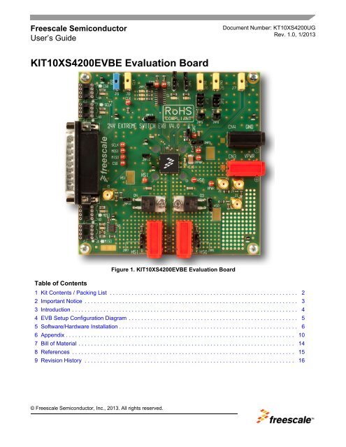
Figure 1. KIT<strong>10</strong>XS4200EVBE Evaluation Board<br />
Document Number: KT<strong>10</strong>XS4200UG<br />
Rev. 1.0, 1/2013<br />
Table of Contents<br />
1 Kit Contents / Packing List . . . . . . . . . . . . . . . . . . . . . . . . . . . . . . . . . . . . . . . . . . . . . . . . . . . . . . . . . . . . 2<br />
2 Important Notice . . . . . . . . . . . . . . . . . . . . . . . . . . . . . . . . . . . . . . . . . . . . . . . . . . . . . . . . . . . . . . . . . . . . 3<br />
3 Introduction . . . . . . . . . . . . . . . . . . . . . . . . . . . . . . . . . . . . . . . . . . . . . . . . . . . . . . . . . . . . . . . . . . . . . . . . 4<br />
4 EVB Setup Configuration Diagram . . . . . . . . . . . . . . . . . . . . . . . . . . . . . . . . . . . . . . . . . . . . . . . . . . . . . . 5<br />
5 Software/Hardware Installation . . . . . . . . . . . . . . . . . . . . . . . . . . . . . . . . . . . . . . . . . . . . . . . . . . . . . . . . . 6<br />
6 Appendix . . . . . . . . . . . . . . . . . . . . . . . . . . . . . . . . . . . . . . . . . . . . . . . . . . . . . . . . . . . . . . . . . . . . . . . . . <strong>10</strong><br />
7 Bill of Material . . . . . . . . . . . . . . . . . . . . . . . . . . . . . . . . . . . . . . . . . . . . . . . . . . . . . . . . . . . . . . . . . . . . . 14<br />
8 References . . . . . . . . . . . . . . . . . . . . . . . . . . . . . . . . . . . . . . . . . . . . . . . . . . . . . . . . . . . . . . . . . . . . . . . 15<br />
9 Revision History . . . . . . . . . . . . . . . . . . . . . . . . . . . . . . . . . . . . . . . . . . . . . . . . . . . . . . . . . . . . . . . . . . . 16
Kit Contents / Packing List<br />
1 Kit Contents / Packing List<br />
• KIT<strong>10</strong>XS4200 Evaluation Board<br />
• CDXS4200<br />
• <strong>Freescale</strong> Warranty Card<br />
KIT<strong>10</strong>XS4200EVBE Evaluation Board, Rev. 1.0<br />
2 <strong>Freescale</strong> <strong>Semiconductor</strong>
2 Important Notice<br />
<strong>Freescale</strong> provides the enclosed product(s) under the following conditions:<br />
This evaluation kit is intended for use of ENGINEERING DEVELOPMENT OR EVALUATION<br />
PURPOSES ONLY. It is provided as a sample IC pre-soldered to a printed circuit board to make<br />
it easier to access inputs, outputs, and supply terminals. This EVB may be used with any<br />
development system or other source of I/O signals by simply connecting it to the host MCU or<br />
computer board via off-the-shelf cables. This EVB is not a Reference Design and is not intended<br />
to represent a final design recommendation for any particular application. Final device in an<br />
application will be heavily dependent on proper printed circuit board layout and heat sinking<br />
design as well as attention to supply filtering, transient suppression, and I/O signal q<strong>ual</strong>ity.<br />
The goods provided may not be complete in terms of required design, marketing, and or<br />
manufacturing related protective considerations, including product safety measures typically<br />
found in the end product incorporating the goods. Due to the open construction of the product, it<br />
is the user's responsibility to take any and all appropriate precautions with regard to electrostatic<br />
discharge. In order to minimize risks associated with the customers applications, adequate design<br />
and operating safeguards must be provided by the customer to minimize inherent or procedural<br />
hazards. For any safety concerns, contact <strong>Freescale</strong> sales and technical support services.<br />
Should this evaluation kit not meet the specifications indicated in the kit, it may be returned within<br />
30 days from the date of delivery and will be replaced by a new kit.<br />
<strong>Freescale</strong> reserves the right to make changes without further notice to any products herein.<br />
<strong>Freescale</strong> makes no warranty, representation or guarantee regarding the suitability of its products<br />
for any particular purpose, nor does <strong>Freescale</strong> assume any liability arising out of the application<br />
or use of any product or circuit, and specifically disclaims any and all liability, including without<br />
limitation consequential or incidental damages. “Typical” parameters can and do vary in different<br />
applications and act<strong>ual</strong> performance may vary over time. All operating parameters, including<br />
“Typical”, must be validated for each customer application by customer’s technical experts.<br />
<strong>Freescale</strong> does not convey any license under its patent rights nor the rights of others. <strong>Freescale</strong><br />
products are not designed, intended, or authorized for use as components in systems intended<br />
for surgical implant into the body, or other applications intended to support or sustain life, or for<br />
any other application in which the failure of the <strong>Freescale</strong> product could create a situation where<br />
personal injury or death may occur.<br />
Should the buyer purchase or use <strong>Freescale</strong> products for any such unintended or unauthorized<br />
application, the buyer shall indemnify and hold <strong>Freescale</strong> and its officers, employees,<br />
subsidiaries, affiliates, and distributors harmless against all claims, costs, damages, and<br />
expenses, and reasonable attorney fees arising out of, directly or indirectly, any claim of personal<br />
injury or death associated with such unintended or unauthorized use, even if such claim alleges<br />
that <strong>Freescale</strong> was negligent regarding the design or manufacture of the part.<strong>Freescale</strong> and the<br />
<strong>Freescale</strong> logo are trademarks of <strong>Freescale</strong> <strong>Semiconductor</strong>, Inc. All other product or service<br />
names are the property of their respective owners. © <strong>Freescale</strong> <strong>Semiconductor</strong>, Inc. 2012<br />
Important Notice<br />
KIT<strong>10</strong>XS4200EVBE Evaluation Board, Rev. 1.0<br />
<strong>Freescale</strong> <strong>Semiconductor</strong> 3
Introduction<br />
3 Introduction<br />
This Extreme <strong>Switch</strong> Evaluation Board User Guide demonstrates the capability of the MC<strong>10</strong>XS4200 as<br />
a <strong>24</strong> V d<strong>ual</strong> high side switch product, that provides integrated control along with a large number of<br />
protective and diagnostic functions.<br />
This product has been designed for truck, bus, and industrial applications. The low RDS(ON) channels<br />
(< <strong>10</strong> mΩ) control different load types; bulb lamps, solenoids, or DC motors. Control, device configuration,<br />
and diagnostics are performed through a 16-bit SPI interface, allowing easy integration into existing<br />
applications.<br />
Both channels can be controlled individ<strong>ual</strong>ly by external/internal clock-signals or by direct inputs. Using<br />
the internal clock allows fully autonomous device operation. Programmable output voltage slew rates<br />
(individ<strong>ual</strong>ly programmable) helps improve EMC performance. To avoid shutting off the device upon<br />
inrush current, while still being able to closely track the load current, a dynamic over-current threshold<br />
profile is featured. <strong>Switch</strong>ing current of each channel can be sensed via a programmable sensing ratio.<br />
Whenever communication with the external microcontroller is lost, the device enters a fail-safe operation<br />
mode, but remains operational, controllable, and protected.<br />
3.1 EVB Features<br />
• Input voltage operation range from 6.0 to 58 V<br />
• D<strong>ual</strong> high side switches<br />
• Programming, control, and diagnostics accomplished via the use of a 16-bit SPI interface<br />
• Output with selectable slew-rate satisfy electromagnetic compatibility (EMC) requirements<br />
• Each output can be controlled with an internal PWM modulated clock signal, instead of an external<br />
clock<br />
3.2 Required Equipment<br />
Minimum required equipment:<br />
• DC power supply capable of supplying up to 50 A at 6.0 to 58 V<br />
• Electronic/resistive loads to load the various power channels<br />
• No cable required<br />
3.3 Optional Equipment for SPI<br />
• 5.0 V Power supply, 1.0 A current capability<br />
• USB enabled computer with Windows XP, Windows 2000, or Windows NT<br />
• CD contains a graphical user interface (GUI) that allows control of all MC<strong>10</strong>XS4200 features via the<br />
SPI<br />
KIT<strong>10</strong>XS4200EVBE Evaluation Board, Rev. 1.0<br />
4 <strong>Freescale</strong> <strong>Semiconductor</strong>
4 EVB Setup Configuration Diagram<br />
PC<br />
via<br />
USB<br />
KITUSBSPIEVME<br />
SPI<br />
Communication<br />
25 Pin Parallel<br />
Connector<br />
5.0 V<br />
Power Supply<br />
KIT<strong>10</strong>XS4200EVBE<br />
Load 1 Load 2<br />
Figure 2. KIT<strong>10</strong>XS4200 Setup Configuration Diagram<br />
EVB Setup Configuration Diagram<br />
<strong>24</strong> V<br />
Power Supply<br />
KIT<strong>10</strong>XS4200EVBE Evaluation Board, Rev. 1.0<br />
<strong>Freescale</strong> <strong>Semiconductor</strong> 5
Software/Hardware Installation<br />
5 Software/Hardware Installation<br />
The KIT<strong>10</strong>XS4200EVBE operates with a single DC power supply from 6.0 to 58 V, and is fully controlled<br />
via the SPI with the help of an USB-SPI KITUSBSPIEVME EVB kit, requiring a 5.0 V DC power supply.<br />
5.1 Starting Up KIT<strong>10</strong>XS4200EVBE<br />
To Start working with KIT<strong>10</strong>XS4200EVBE, provide <strong>24</strong> V input voltage between 6.0 to 58 V, by connecting<br />
the (+) probe to the Star VPWR pin, and the (-) probe to the GND pin, on the input power terminal block.<br />
Then apply a 5.0 V input voltage between VDD and the GND terminal. The load is connected between<br />
the HS0 (or HS1) pin and the (-) terminal with the <strong>24</strong> V power supply.<br />
5.2 Controlling KIT<strong>10</strong>XS4200EVBE via the SPI<br />
The KITUSBSPIEVME EVB kit enables interaction with the KIT<strong>10</strong>XS4200EVBE. Full operation of the<br />
MC<strong>10</strong>XS4200 device is achieved via use of the graphical user interface developed by <strong>Freescale</strong>.<br />
Note: SPI mapping is similar for all three User Guides (KT06, KT<strong>10</strong>, and KT20XS4200UG).<br />
5.3 Initializing SPIGen<br />
Once SPIGen has been successfully installed, the following screen appears:<br />
Figure 3. SPIGen after First Installation<br />
KIT<strong>10</strong>XS4200EVBE Evaluation Board, Rev. 1.0<br />
6 <strong>Freescale</strong> <strong>Semiconductor</strong>
5.4 SPD<strong>10</strong> Configuration<br />
To configure SPD<strong>10</strong>, download the Config SPI file.<br />
Select File, Open, then SPD<strong>10</strong>_config.file.:<br />
Figure 4. SPD<strong>10</strong> Configuration<br />
Software/Hardware Installation<br />
KIT<strong>10</strong>XS4200EVBE Evaluation Board, Rev. 1.0<br />
<strong>Freescale</strong> <strong>Semiconductor</strong> 7
Software/Hardware Installation<br />
5.5 SPD<strong>10</strong> Initialization<br />
To control the device, do the following:<br />
• Set R STB to level high by entering Extra Pins into the Radio Box<br />
• Set Control0 = <strong>High</strong><br />
• Set Bit 6 of SO to 1<br />
• Click Send Once<br />
Figure 5. SPD<strong>10</strong> Initialization<br />
KIT<strong>10</strong>XS4200EVBE Evaluation Board, Rev. 1.0<br />
8 <strong>Freescale</strong> <strong>Semiconductor</strong>
5.6 SPD<strong>10</strong> Enhanced Initialization<br />
Software/Hardware Installation<br />
If you want to initialize the device more quickly, select the Send a Batch of Commands tab, select Init<br />
for the setup, and then Click on Send Once.<br />
Figure 6. SPD<strong>10</strong> Enhanced Initialization<br />
KIT<strong>10</strong>XS4200EVBE Evaluation Board, Rev. 1.0<br />
<strong>Freescale</strong> <strong>Semiconductor</strong> 9
Appendix<br />
6 Appendix<br />
6.1 KIT<strong>10</strong>XS4200EVBE Schematic<br />
8<br />
7<br />
6<br />
5<br />
4<br />
3<br />
2<br />
1<br />
J<strong>10</strong><br />
HS 0<br />
CN 1<br />
B ANANA _R ED<br />
GND<br />
8<br />
GND<br />
R1 0<br />
0R<br />
CB AN2 6.8nF<br />
C8<br />
22nF<br />
R6<br />
2.2k<br />
J1<br />
SM A<br />
GND<br />
U5<br />
Anode<br />
Cathode<br />
GND<br />
GND<br />
HF BR1528<br />
1<br />
2<br />
3<br />
4<br />
R5<br />
47R<br />
VDD<br />
GND<br />
5<br />
GND<br />
GND<br />
GND<br />
R1<br />
2k7<br />
C2<br />
<strong>10</strong>0nF<br />
C1<br />
1uF<br />
GND<br />
GND<br />
D<br />
D1<br />
LED R<br />
D<br />
RBA N2<br />
51RGN<br />
D<br />
1 2<br />
JM P6<br />
1 2<br />
2PTS<br />
3<br />
8<br />
R2 5<br />
<strong>10</strong>k<br />
JM P1<br />
2PTS<br />
GN D<br />
8<br />
GND<br />
GN D<br />
5<br />
1<br />
2<br />
3<br />
4<br />
GND<br />
8<br />
GND<br />
HS 1<br />
CN 2<br />
B ANANA _R ED<br />
5<br />
1<br />
2<br />
3<br />
4<br />
GND<br />
R1 1<br />
0R<br />
CB AN3 6.8nF<br />
C9<br />
22nF<br />
R7<br />
2.2k<br />
J2<br />
SM A<br />
GND<br />
8<br />
GND<br />
GN D<br />
D2<br />
LED R<br />
5<br />
1<br />
2<br />
3<br />
4<br />
GND<br />
RB AN3<br />
51R GN D<br />
U2<br />
VO<br />
GND<br />
VC C<br />
NC<br />
HF BR2528<br />
U3<br />
VO<br />
GND<br />
VC C<br />
NC<br />
HF BR2528<br />
U4<br />
VO<br />
GND<br />
VC C<br />
NC<br />
HF BR2528<br />
U1A<br />
SN75451<br />
1<br />
2<br />
GND<br />
MOSI<br />
GND<br />
R2 4<br />
<strong>10</strong>k<br />
MI SO<br />
JP1<br />
D3<br />
MU R840<br />
R2<br />
2.7R<br />
VDD<br />
4<br />
GND<br />
C3<br />
<strong>10</strong>0nF<br />
GND<br />
GND<br />
J11<br />
GND<br />
GND<br />
SC LK<br />
GND<br />
TP 12<br />
TSTP T<br />
TP 13<br />
TSTP T<br />
TP <strong>10</strong><br />
TSTP T<br />
R3<br />
2.7R<br />
VDD<br />
GND<br />
C4<br />
<strong>10</strong>0nF<br />
GND<br />
JM P7<br />
1 2<br />
2PTS<br />
GND<br />
CS B<br />
GND<br />
R4<br />
2.7R<br />
VDD<br />
JM P<strong>10</strong><br />
2PTS<br />
1 2<br />
GND<br />
C5<br />
<strong>10</strong>0nF<br />
GN D<br />
GND<br />
RS TB _ 1<br />
14<br />
CS B 2<br />
15<br />
MOSI 3<br />
FS 0B 16<br />
SC LK 4<br />
FS B 17<br />
IN 0J 5<br />
18<br />
IN 1J 6<br />
19<br />
SYNC 7<br />
20<br />
CONF 0 8<br />
21<br />
CONF 1 9<br />
22<br />
<strong>10</strong><br />
23<br />
11<br />
<strong>24</strong><br />
MI SO 12<br />
25<br />
13<br />
C<br />
D4 GN D<br />
MU R840<br />
GN D<br />
J5<br />
1<br />
1<br />
EM _2MM_ JAUN E<br />
TP 11<br />
TSTP T<br />
C<br />
J6<br />
1<br />
EM _2MM_ JAUN E<br />
1<br />
JP2<br />
1 2<br />
IN 0 IN 0J<br />
3 4<br />
VDD<br />
5 6<br />
R2 2<br />
RE S1 HE AD ER 3X 2<br />
JM P8<br />
1 2<br />
2PTS<br />
D<strong>10</strong><br />
JP3<br />
LED R<br />
1 2<br />
IN 1 IN 1J<br />
3 4<br />
VDD<br />
GND<br />
5 6<br />
R2 3<br />
RE S1 HE ADE R3 X2<br />
JM P9<br />
1 2<br />
2PTS<br />
D11<br />
LED R<br />
DB 25<br />
RS TB _<br />
JM P13<br />
1<br />
2<br />
3<br />
JUMP 3<br />
RS TB<br />
VDD<br />
Figure 7. MC<strong>10</strong>XS4200 Schematic<br />
KIT<strong>10</strong>XS4200EVBE Evaluation Board, Rev. 1.0<br />
<strong>10</strong> <strong>Freescale</strong> <strong>Semiconductor</strong><br />
TP 2<br />
TSTP T<br />
SV PW R<br />
VP WR<br />
TP 1 TST PT<br />
15<br />
18<br />
21<br />
C6<br />
<strong>10</strong>0nF<br />
B<br />
CS NS<br />
IN 0<br />
IN 1<br />
FS0 B<br />
CONF 0<br />
CONF 1<br />
FSB<br />
CL OC K<br />
RS TB<br />
CS B<br />
SC LK<br />
MOSI<br />
VDD<br />
MI SO<br />
SYNC<br />
1<br />
2<br />
3<br />
4<br />
5<br />
6<br />
7<br />
8<br />
9<br />
<strong>10</strong><br />
11<br />
12<br />
13<br />
16<br />
23<br />
U6 SP D<strong>10</strong><br />
CS NS<br />
IN 0<br />
IN 1<br />
HS 1<br />
FSO<br />
CONF 0<br />
CONF 1<br />
FS<br />
CL OC K<br />
HS 0<br />
RS T<br />
CS<br />
SC LK<br />
SI<br />
VDD<br />
SO<br />
SYNC<br />
GND<br />
VPWR<br />
VPWR<br />
VPWR<br />
19<br />
HS 1<br />
GN D<br />
J12<br />
GND<br />
SHS1<br />
TP 3 TST PT<br />
VP WR<br />
C16<br />
1uF<br />
GND<br />
18121C<strong>10</strong>5K A<br />
CN 4<br />
CN 3<br />
GND<br />
B ANANA_ BL AC K B ANANA _R ED<br />
R8<br />
RE S1<br />
20<br />
HS 0<br />
B<br />
J3<br />
SM A<br />
R1 2<br />
0R<br />
CB AN1 6.8nF<br />
SHS0<br />
TP 4 TST PT<br />
J4<br />
SM A<br />
TP 7<br />
TSTP T<br />
TP 6<br />
TSTP T<br />
TP 9<br />
TSTP T<br />
J8<br />
1<br />
1<br />
EM _2MM_ JAUN E<br />
J9<br />
1<br />
1<br />
C7<br />
<strong>10</strong>0nF<br />
EM _2MM_B LEU<br />
GN D<br />
GN D<br />
GN D<br />
FS0 B<br />
FSB<br />
RBA N1<br />
51R GN D<br />
TP 8<br />
TSTP T<br />
GND<br />
R2 0<br />
<strong>10</strong>0k<br />
R1 9<br />
<strong>10</strong>k<br />
17<br />
22<br />
14<br />
1<br />
CS NS<br />
C17<br />
22nF<br />
JM P11<br />
2PTS<br />
2<br />
R1 3<br />
1k<br />
R2 1<br />
1k_0.1%<br />
VP WR<br />
VD D<br />
GND<br />
GND<br />
VD D<br />
JM P2<br />
1 2<br />
2PTS<br />
JM P12<br />
2PTS<br />
1 2<br />
JM P5<br />
1<br />
2<br />
3<br />
JUMP 3<br />
VD D<br />
JM P4<br />
1<br />
2<br />
3<br />
JUMP 3<br />
VD D<br />
GND<br />
1<br />
GN D<br />
CONF 0<br />
R1 6<br />
1k<br />
D5<br />
CONF 1<br />
R1 7<br />
1k<br />
GND<br />
GN D<br />
LE DV<br />
U7A<br />
3 2 R1 4<br />
1k<br />
MC74H C4049<br />
FSB<br />
GN D<br />
8<br />
VDD<br />
TP 5<br />
TSTP T<br />
A<br />
D9<br />
LED V<br />
D8<br />
LED V<br />
D6<br />
R1 8<br />
<strong>10</strong>k<br />
A<br />
R1 5<br />
1k<br />
FS0 B<br />
SYNC<br />
GND<br />
GN D<br />
GND<br />
LED V<br />
GND<br />
U7B<br />
5 4<br />
MC74H C4049<br />
JM P3<br />
1<br />
2<br />
3<br />
J7<br />
1 JUMP 3<br />
1<br />
EM _2MM_J AUN E<br />
TSTP TTSTP<br />
TTSTP<br />
TTSTP<br />
TTSTP<br />
TTSTP<br />
TTSTP<br />
T<br />
TP 14 TP 15 TP 16 TP 17 TP 18 TP 19 TP 20<br />
E rror : FS_ COLO R_LO GO_JPG.jpg file not found.<br />
TitleSPD<br />
<strong>10</strong> Application<br />
Si ze: A3 Number: 1 Revision: 3.0<br />
Date: 12-Apr-2011 Version 4 April 2011<br />
Sheet1 of 1<br />
D7<br />
GND<br />
R9<br />
RE S1<br />
7 6<br />
U7C<br />
RS TB<br />
LED V<br />
MC74H C4049<br />
GN D<br />
1 2 3 4 5 6 7 8
6.2 KIT<strong>10</strong>XS4200EVBE Assembly Layer Top<br />
_<br />
Figure 8. KIT<strong>10</strong>XS4200EVBE Assembly Layer Top<br />
Appendix<br />
KIT<strong>10</strong>XS4200EVBE Evaluation Board, Rev. 1.0<br />
<strong>Freescale</strong> <strong>Semiconductor</strong> 11
Appendix<br />
6.3 KIT<strong>10</strong>XS4200EVBE Assembly Layer Bottom<br />
Figure 9. KIT<strong>10</strong>XS4200EVBE Assembly Layer Bottom<br />
KIT<strong>10</strong>XS4200EVBE Evaluation Board, Rev. 1.0<br />
12 <strong>Freescale</strong> <strong>Semiconductor</strong>
6.4 KIT<strong>10</strong>XS4200EVBE Silkscreen<br />
Figure <strong>10</strong>. KIT<strong>10</strong>XS4200EVBE Silkscreen<br />
Appendix<br />
KIT<strong>10</strong>XS4200EVBE Evaluation Board, Rev. 1.0<br />
<strong>Freescale</strong> <strong>Semiconductor</strong> 13
Bill of Material<br />
7 Bill of Material<br />
Table 1. KIT<strong>10</strong>XS4200 Bill of Material<br />
ITEM QTY PART DESIGNATION VALUE / RATING PART NUMBER / MANUFACTURER<br />
RESISTORS<br />
1 1 R1 2.0 k7 Resitor 1%, SMD<br />
2 3 R2, R3, R4 2.7 R Resitor 1%, SMD<br />
3 1 R5 47 R Resitor 1%, SMD<br />
4 2 R6, R7 2.2.0 k Resitor 1%, SMD<br />
5 3 R<strong>10</strong>, R11, R12 0 R Resitor 1%, SMD<br />
6 5 R13, R14, R15, R16, R17 1.0 k Resitor 1%, SMD<br />
7 4 R18, R19, R<strong>24</strong>, R25 <strong>10</strong> k Resitor 1%, SMD<br />
8 1 R20 <strong>10</strong>0 k Resitor 1%, SMD<br />
9 1 R21 1.0 k Resitor 0,1%, SMD<br />
CAPACITORS<br />
<strong>10</strong> 2 C1, C16 1.0 uF Capacitor Ceramic 50 V<br />
11 6 C2, C3, C4, C5, C6, C7 <strong>10</strong>0nF Capacitor Ceramic 50 V<br />
12 3 C 8, C9, C17 22nF Capacitor Ceramic 50 V<br />
13 3 CBAN1, CBAN2, CBAN3 6.8 nF Capacitor Ceramic 50 V<br />
DIODES<br />
14 4 D1, D2, D<strong>10</strong>, D11 LEDR Diode LED red<br />
15 2 D3, D4 MUR840 Rectified diode 7.0 A, 400 V<br />
16 5 D5, D6, D7, D8, D9 LEDV Diode LED green<br />
ACTIVE COMPONENTS<br />
17 1 U7 MC74HC4049 Buffer/Converter Hex Inv CMOS<br />
18 1 U1 SN75451 D<strong>ual</strong> peripheral driver<br />
19 1 U6 MC<strong>10</strong>XS4200FK SPD<strong>10</strong> <strong>Freescale</strong> device<br />
<strong>Freescale</strong> Disclaimer:<br />
<strong>Freescale</strong> does not assume liability, endorse, or warrant components from external manufacturers that are referenced in circuit drawings or<br />
tables. While <strong>Freescale</strong> offers component recommendations in this configuration, it is the customer’s responsibility to validate their<br />
application.<br />
KIT<strong>10</strong>XS4200EVBE Evaluation Board, Rev. 1.0<br />
14 <strong>Freescale</strong> <strong>Semiconductor</strong>
References<br />
8 References<br />
The following list contains URLs where you can obtain information on other <strong>Freescale</strong> products and<br />
MC<strong>10</strong>XS4200 product solutions:<br />
8.1 Support<br />
Visit <strong>Freescale</strong>.com/support for a list of phone numbers within your region.<br />
8.2 Warranty<br />
DESCRIPTION URL<br />
MC<strong>10</strong>XS4200 Product Summary Page http://www.freescale.com/webapp/sps/site/prod_summary.jsp?code=MC<strong>10</strong>XS4200<br />
MC<strong>10</strong>XS4200 Data Sheet http://cache.freescale.com/files/analog/doc/data_sheet/MC<strong>10</strong>XS4200<br />
MC<strong>10</strong>XS4200 Fact Sheet http://cache.freescale.com/files/analog/doc/fact_sheet/MC<strong>10</strong>XS4200FS.pdf<br />
SPIGEN Reference http://cache.freescale.com/files/soft_dev_tools/software/device_drivers/SPIGen.html<br />
<strong>Freescale</strong>’s Analog Web Site www.freescale.com/analog<br />
<strong>Freescale</strong>’s Automotive Applications Web Site www.freescale.com/automotive<br />
Visit <strong>Freescale</strong>.com/warranty for for complete warranty information.<br />
KIT<strong>10</strong>XS4200EVBE Evaluation Board, Rev. 1.0<br />
<strong>Freescale</strong> <strong>Semiconductor</strong> 15
Revision History<br />
9 Revision History<br />
REVISION DATE DESCRIPTION OF CHANGES<br />
1.0 1/2013 • Initial Release<br />
KIT<strong>10</strong>XS4200EVBE Evaluation Board, Rev. 1.0<br />
16 <strong>Freescale</strong> <strong>Semiconductor</strong>
How to Reach Us:<br />
Home Page:<br />
freescale.com<br />
Web Support:<br />
freescale.com/support<br />
Document Number: KT<strong>10</strong>XS4200UG<br />
Rev. 1.0<br />
1/2013<br />
Information in this document is provided solely to enable system and software<br />
implementers to use <strong>Freescale</strong> products. There are no express or implied copyright<br />
licenses granted hereunder to design or fabricate any integrated circuits on the<br />
information in this document.<br />
<strong>Freescale</strong> reserves the right to make changes without further notice to any products<br />
herein. <strong>Freescale</strong> makes no warranty, representation, or guarantee regarding the<br />
suitability of its products for any particular purpose, nor does <strong>Freescale</strong> assume any<br />
liability arising out of the application or use of any product or circuit, and specifically<br />
disclaims any and all liability, including without limitation consequential or incidental<br />
damages. “Typical” parameters that may be provided in <strong>Freescale</strong> data sheets and/or<br />
specifications can and do vary in different applications, and act<strong>ual</strong> performance may<br />
vary over time. All operating parameters, including “typicals,” must be validated for<br />
each customer application by customer’s technical experts. <strong>Freescale</strong> does not convey<br />
any license under its patent rights nor the rights of others. <strong>Freescale</strong> sells products<br />
pursuant to standard terms and conditions of sale, which can be found at the following<br />
address: http://www.reg.net/v2/webservices/<strong>Freescale</strong>/Docs/TermsandConditions.htm<br />
<strong>Freescale</strong>, the <strong>Freescale</strong> logo, AltiVec, C-5, CodeTest, CodeWarrior, ColdFire, C-Ware,<br />
Energy Efficient Solutions logo, mobileGT, PowerQUICC, QorIQ, Qorivva, StarCore, and<br />
Symphony are trademarks of <strong>Freescale</strong> <strong>Semiconductor</strong>, Inc., Reg. U.S. Pat. & Tm. Off.<br />
Airfast, BeeKit, BeeStack, ColdFire+, CoreNet, Flexis, MagniV, MXC, Platform in a<br />
Package, Processor expert, QorIQ Qonverge, QUICC Engine, Ready Play,<br />
SMARTMOS, TurboLink, Vybrid, and Xtrinsic are trademarks of <strong>Freescale</strong><br />
<strong>Semiconductor</strong>, Inc. All other product or service names are the property of their<br />
respective owners.<br />
© 2013 <strong>Freescale</strong> <strong>Semiconductor</strong>, Inc.


