

MC34827, Mini or Micro-USB Interface IC - Freescale Semiconductor
MC34827, Mini or Micro-USB Interface IC - Freescale Semiconductor
MC34827, Mini or Micro-USB Interface IC - Freescale Semiconductor

You also want an ePaper? Increase the reach of your titles
YUMPU automatically turns print PDFs into web optimized ePapers that Google loves.
<strong>Freescale</strong> Semiconduct<strong>or</strong><br />
Advance Inf<strong>or</strong>mation<br />
<strong>Mini</strong> <strong>or</strong> <strong>Micro</strong>-<strong>USB</strong> <strong>Interface</strong> <strong>IC</strong><br />
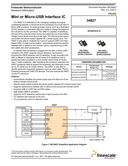
The 34827 is a dedicated <strong>IC</strong> f<strong>or</strong> managing charging and signal<br />
multiplexing between a cell phone and its access<strong>or</strong>y via a 5-pin <strong>Mini</strong> <strong>or</strong><br />
<strong>Micro</strong>-<strong>USB</strong> connect<strong>or</strong>. An external power source, such as a dedicated<br />
AC/DC adapter <strong>or</strong> a standard <strong>USB</strong> p<strong>or</strong>t, is able to charge the battery in<br />
the cell phone via the connect<strong>or</strong>. The 34827 is capable of identifying<br />
the type of the external power source and selecting one of two battery<br />
charge current levels acc<strong>or</strong>ding to the type. The internal power switch<br />
can protect the phone system against 28 V power supply input. The<br />
34827 is also able to multiplex the 5 pins to supp<strong>or</strong>t UART and High-<br />
Speed <strong>USB</strong> 2.0 data communication, mono/stereo-audio/microphone<br />
headset with <strong>or</strong> without a c<strong>or</strong>d remote control, manufacturing <strong>or</strong> R/D<br />
test cables and other access<strong>or</strong>ies.<br />
To identify what access<strong>or</strong>y is plugged into the <strong>Mini</strong> <strong>or</strong> <strong>Micro</strong>-<strong>USB</strong><br />
connect<strong>or</strong>, the 34827 supp<strong>or</strong>ts various detection mechanisms,<br />
including the VBUS detection and ID detection. A high accurate 5-bit<br />
ADC is offered to distinguish the 32 levels of ID resistance and to<br />
identify the button pressed in a c<strong>or</strong>d remote control while an Audio<br />
Type 1 cable is attached. After identifying the access<strong>or</strong>y attached, the<br />
34827 configures itself to supp<strong>or</strong>t the access<strong>or</strong>y and interrupts a host<br />
via an I 2 C serial bus f<strong>or</strong> further actions. The 34827 is also able to<br />
identify some non-supp<strong>or</strong>ted access<strong>or</strong>y, such as video cable, Phone-<br />
Powered Devices and <strong>USB</strong> OTG devices. The host controls the 34827<br />
via the I 2 C serial bus.<br />
34827<br />
(PB-FREE)<br />
98ASA00050D<br />
20-PIN UTQFN-EP<br />
Device<br />
<strong>MC34827</strong>A2EP/R2<br />
Features<br />
<strong>MC34827</strong>A1EP/R2<br />
• Automatically identifies the power supply type and sets one of two<br />
battery-charge-current levels<br />
• Internal power switch protects the phone system against 28 V power supply input<br />
• Supp<strong>or</strong>ts stereo/mono headset with <strong>or</strong> without micro phone and remote control<br />
• Supp<strong>or</strong>ts <strong>USB</strong> <strong>or</strong> UART test and R/D cables<br />
• High speed <strong>USB</strong>2.0 compliant<br />
• Supp<strong>or</strong>ts 32 ID resistance values with a high-accuracy 5-bit ADC<br />
• I2C interface with interrupt to the host<br />
• 10 μA quiescent current in Standby mode<br />
BASEBAND<br />
GPIO<br />
I 2 C<br />
UART<br />
<strong>USB</strong> XCVR<br />
Test P<strong>or</strong>t<br />
Audio<br />
VDDIO<br />
INTB<br />
I2C_SDA<br />
I2C_SCL<br />
RXD<br />
TXD<br />
34827<br />
*This document contains certain inf<strong>or</strong>mation on a product under development. <strong>Freescale</strong><br />
reserves the right to change <strong>or</strong> discontinue this product without notice<br />
D+<br />
D-<br />
JIG<br />
BOOT<br />
SPK_L<br />
SPK_R<br />
M<strong>IC</strong><br />
© <strong>Freescale</strong> Semiconduct<strong>or</strong>, Inc., 2011. All rights reserved.<br />
VDD<br />
ISET<br />
OUT<br />
VBUS<br />
ID<br />
DP<br />
DM<br />
GND<br />
Document Number: <strong>MC34827</strong><br />
Rev. 2.0, 3/2011<br />
INTERFACE <strong>IC</strong><br />
ORDERING INFORMATION<br />
Li+<br />
Figure 1. <strong>MC34827</strong> Simplified Application Diagram<br />
Temperature<br />
Range (T A )<br />
-40 to 85 °C<br />
Charger<br />
(PB-FREE)<br />
98ASA00037D<br />
20-PIN UTQFN-EP<br />
Package<br />
3.0 mm X 4.0 mm<br />
UTQFN-EP<br />
3.0 mm X 3.0 mm<br />
UTQFN-EP<br />
V BUS<br />
ID<br />
D+<br />
D-<br />
GND<br />
<strong>USB</strong> CONNECTOR
INTERNAL BLOCK DIAGRAM<br />
<strong>MC34827</strong><br />
VDDIO<br />
I2C_SDA<br />
I2C_SCL<br />
INTB<br />
JIG<br />
BOOT<br />
RxD<br />
TxD<br />
D+<br />
D-<br />
SPK_R<br />
SPK_L<br />
M<strong>IC</strong><br />
INTERNAL BLOCK DIAGRAM<br />
Reset<br />
I2C<br />
<strong>Interface</strong><br />
Interrupt<br />
JIG<br />
Logic<br />
Output<br />
UART<br />
Switches<br />
<strong>USB</strong><br />
Switches<br />
Audio<br />
Switches<br />
OSC<br />
VBUS<br />
Detect<br />
Registers<br />
&<br />
State<br />
Machine<br />
ID ADC<br />
ID<br />
Detect<br />
Analog Integrated Circuit Device Data<br />
2 <strong>Freescale</strong> Semiconduct<strong>or</strong><br />
VBUS<br />
Internal<br />
Supplies<br />
Gate<br />
Drive &<br />
OCP<br />
Figure 2. <strong>MC34827</strong> Simplified Internal Block Diagram<br />
VDD<br />
VBUS<br />
OUT<br />
ISET<br />
DP<br />
DM<br />
ID<br />
GND
SPK_R<br />
SPK_L<br />
M<strong>IC</strong><br />
D+<br />
D-<br />
RxD<br />
2<br />
3<br />
4<br />
5<br />
6<br />
ID<br />
20<br />
7<br />
DP<br />
DM<br />
19<br />
8<br />
18<br />
9<br />
VBUS<br />
17<br />
1 16<br />
TxD<br />
21<br />
GND<br />
BOOT<br />
VDDIO<br />
10<br />
JIG<br />
15<br />
14<br />
13<br />
12<br />
11<br />
ISET<br />
OUT<br />
I2C_SCL<br />
I2C_SDA<br />
INTB<br />
VDD<br />
(A). Pinout of 34827 Using a 3.0 mm X 4.0 mm 20 Pin. UTQFN Package<br />
(Transparent Top View)<br />
Table 1. <strong>MC34827</strong> Pin Definitions<br />
PIN CONNECTIONS<br />
SPK_R<br />
PIN CONNECTIONS<br />
<strong>MC34827</strong><br />
Analog Integrated Circuit Device Data<br />
<strong>Freescale</strong> Semiconduct<strong>or</strong> 3<br />
SPK_L<br />
M<strong>IC</strong><br />
D+<br />
D-<br />
Figure 3. <strong>MC34827</strong> Pin Connections<br />
1<br />
2<br />
3<br />
4<br />
5<br />
ID<br />
20<br />
6<br />
RxD<br />
DP<br />
DM<br />
19<br />
7<br />
TxD<br />
18<br />
21<br />
GND<br />
8<br />
BOOT<br />
VBUS<br />
17<br />
9<br />
VDDIO<br />
ISET<br />
16<br />
10<br />
JIG<br />
15<br />
14<br />
13<br />
12<br />
11<br />
OUT<br />
I2C_SCL<br />
I2C_SDA<br />
INTB<br />
VDD<br />
(B). Pinout of 34827 Using a 3.0 mm X 3.0 mm 20 Pin. UTQFN Package<br />
(Transparent Top View)<br />
A functional description of each pin can be found in the Functional Pin Description section beginning on page 13.<br />
Pin Number Pin Name Pin Function F<strong>or</strong>mal Name Definition<br />
1 SPK_R Input Speaker right channel Right channel input of the speaker signals<br />
2 SPK_L Input Speaker left channel Left channel input of the speaker signals<br />
3 M<strong>IC</strong> Output <strong>Micro</strong>phone output <strong>Micro</strong>phone output to the baseband of the cell phone system<br />
4 D+ IO D+ of the <strong>USB</strong><br />
transceiver<br />
5 D- IO D- of the <strong>USB</strong><br />
transceiver<br />
D+ line of the <strong>USB</strong> transceiver<br />
D- line of the <strong>USB</strong> transceiver<br />
6 RxD Output UART receiver Receive line of the UART<br />
7 TxD Input UART transmitter Transmit line of the UART<br />
8 BOOT Output BOOT indicat<strong>or</strong> Push-pull output to indicate the boot switch setting of the jig cable<br />
9 VDDIO Input IO power supply IO supply voltage. This is the internal supply voltage f<strong>or</strong> the BOOT and<br />
INTB outputs. It can supply the external pull-up voltages f<strong>or</strong> the JIG pin<br />
and the I 2 C bus outside the 34827. This pin also functions as the<br />
hardware reset to the <strong>IC</strong>.<br />
10 JIG Output JIG indicat<strong>or</strong> Open-drain output to indicate the insertion of a jig cable<br />
11 VDD Input Power supply Supply input<br />
12 INTB Output Interrupt output Push-pull interrupt output<br />
13 I2C_SDA IO I 2 C Data Data line of the I 2 C interface<br />
14 I2C_SCL Input I 2 C Clock Clock line of the I 2 C interface<br />
15 OUT Output Power output The output of the power MOSFET pass switch<br />
16 ISET Output Charge current setting Open-drain output to set the charger current<br />
17 VBUS Input VBUS power supply <strong>Mini</strong>-<strong>USB</strong> VBUS line
PIN CONNECTIONS<br />
Table 1. <strong>MC34827</strong> Pin Definitions (continued)<br />
A functional description of each pin can be found in the Functional Pin Description section beginning on page 13.<br />
Pin Number Pin Name Pin Function F<strong>or</strong>mal Name Definition<br />
<strong>MC34827</strong><br />
18 DM IO D- of the <strong>USB</strong><br />
connect<strong>or</strong><br />
19 DP IO D+ of the <strong>USB</strong><br />
connect<strong>or</strong><br />
20 ID Input ID of the <strong>USB</strong><br />
connect<strong>or</strong><br />
21 GND Ground Ground Ground<br />
D- line of the mini-<strong>USB</strong> connect<strong>or</strong><br />
D+ line of the mini-<strong>USB</strong> connect<strong>or</strong><br />
ID pin of the mini-<strong>USB</strong> connect<strong>or</strong><br />
Analog Integrated Circuit Device Data<br />
4 <strong>Freescale</strong> Semiconduct<strong>or</strong>
Table 2. Maximum Ratings<br />
ELECTR<strong>IC</strong>AL CHARACTERIST<strong>IC</strong>S<br />
MAXIMUM RATINGS<br />
ELECTR<strong>IC</strong>AL CHARACTERIST<strong>IC</strong>S<br />
MAXIMUM RATINGS<br />
All voltages are with respect to ground, unless otherwise noted. Exceeding these ratings may cause a malfunction <strong>or</strong><br />
permanent damage to the device.<br />
ELECTR<strong>IC</strong>AL RATINGS<br />
Input Voltage Range<br />
VBUS Pin<br />
OUT Pin<br />
VDD Pin<br />
VDDIO Pin (1)<br />
SPK_L, SPK_R, DP and DM Pins<br />
All Other Pins<br />
ESD Voltage (2)<br />
Air Gap Discharge Model f<strong>or</strong> VBUS, DP, DM, ID Pins (3)<br />
Human Body Model (HBM) f<strong>or</strong> VBUS, DP, DM, ID Pins<br />
Human Body Model (HBM) f<strong>or</strong> all other pins<br />
Machine Model (MM)<br />
THERMAL RATINGS<br />
Ratings Symbol Value Unit<br />
<strong>MC34827</strong><br />
Analog Integrated Circuit Device Data<br />
<strong>Freescale</strong> Semiconduct<strong>or</strong> 5<br />
VBUS VOUT VDD VDDIO V ESD<br />
-0.3 to 28<br />
-0.3 to 8<br />
-0.3 to 6<br />
-0.3 to 4.2<br />
-2.0 to VDD+0.3 -0.3 to 5.5<br />
±15000<br />
±8000<br />
±2000<br />
±200<br />
Operating Temperature<br />
°C<br />
Ambient<br />
TA -40 to +85<br />
Junction<br />
TJ 150<br />
St<strong>or</strong>age Temperature TSTG -65 to +150 °C<br />
Thermal Resistance (4)<br />
Junction-to-Case<br />
Junction-to-Ambient<br />
Peak Package Reflow Temperature During Reflow (5) , (6)<br />
°C/W<br />
RθJC 6<br />
RθJA 45<br />
TPPRT Note 6 °C<br />
Notes<br />
1. The VDDIO pin CANNOT exceed a maximum voltage of 4.2 V, else it will suffer permanent damage.<br />
2. ESD testing is perf<strong>or</strong>med in acc<strong>or</strong>dance with the Human Body Model (HBM) (CZAP = 100 pF, RZAP = 1500 Ω), and the Machine Model<br />
(MM) (CZAP = 200 pF, RZAP = 0 Ω).<br />
3. Need external ESD protection diode array to meet IEC1000-4-2 15000V air gap discharge requirement (CZAP = 150 pF, RZAP = 330 Ω).<br />
4. Device mounted on the <strong>Freescale</strong> EVB test board per JEDEC DESD51-2.<br />
5. Pin soldering temperature limit is f<strong>or</strong> 10 seconds maximum duration. Not designed f<strong>or</strong> immersion soldering. Exceeding these limits may<br />
cause malfunction <strong>or</strong> permanent damage to the device.<br />
6. <strong>Freescale</strong>’s Package Reflow capability meets Pb-free requirements f<strong>or</strong> JEDEC standard J-STD-020C. F<strong>or</strong> Peak Package Reflow<br />
Temperature and Moisture Sensitivity Levels (MSL), go to www.freescale.com, search by part number, e.g. remove prefixes/suffixes and<br />
enter the c<strong>or</strong>e ID to view all <strong>or</strong>derable parts. (i.e. MC33xxxD enter 33xxx), and review parametrics.<br />
V<br />
V
ELECTR<strong>IC</strong>AL CHARACTERIST<strong>IC</strong>S<br />
STAT<strong>IC</strong> ELECTR<strong>IC</strong>AL CHARACTERIST<strong>IC</strong>S<br />
Table 3. Static Electrical Characteristics<br />
<strong>MC34827</strong><br />
STAT<strong>IC</strong> ELECTR<strong>IC</strong>AL CHARACTERIST<strong>IC</strong>S<br />
Characteristics noted under conditions V DD = 3.6 V, V BUS = 5.0 V, V DDIO = 3.0 V, -40 °C ≤ T A ≤ 85 °C (see Figure 1), unless<br />
otherwise noted. Typical values noted reflect the approximate parameter means at V DD = 3.6 V and T A = 25 °C under nominal<br />
conditions, unless otherwise noted.<br />
POWER INPUT<br />
Characteristic Symbol Min Typ Max Unit<br />
Recommended Operating Voltage Range f<strong>or</strong> VDD Supply Voltage V DD 2.7 - 5.5 V<br />
VDD Power-on Reset Threshold<br />
Rising edge<br />
Hysteresis<br />
VDD Quiescent Current<br />
In Standby mode<br />
In Power Save mode<br />
When access<strong>or</strong>y is attached & INT_MASK = ‘1’<br />
In Active mode (VDD < VBUS)<br />
In Active mode (VDD > VBUS)<br />
V VDDPOR<br />
VBUS Supply Voltage V BUS 2.8 5.0 28 V<br />
VBUS Detection Threshold Voltage<br />
Rising edge<br />
Hysteresis<br />
VBUS Supply Quiescent Current<br />
In VBUS power mode<br />
In Active mode - Dedicated Charger<br />
In Active mode - Audio <strong>or</strong> TTY (7) (VBUS < VDD)<br />
VBUS Over-voltage Protection Threshold<br />
Rising edge<br />
Hysteresis<br />
VBUS Over-current Protection<br />
Triggering threshold (at onset of OTP shutoff)<br />
Over-temperature Protection Threshold<br />
Rising threshold<br />
Falling threshold<br />
Analog Integrated Circuit Device Data<br />
6 <strong>Freescale</strong> Semiconduct<strong>or</strong><br />
I VDD<br />
V BUS_DET<br />
I VBUS<br />
V BUS_OVP<br />
I BUS_OCP<br />
T OTP<br />
-<br />
-<br />
-<br />
-<br />
-<br />
-<br />
-<br />
-<br />
-<br />
-<br />
-<br />
-<br />
6.8<br />
-<br />
2.5<br />
100<br />
9.0<br />
12<br />
125<br />
550<br />
850<br />
2.65<br />
150<br />
-<br />
-<br />
-<br />
7.0<br />
150<br />
2.65<br />
-<br />
12<br />
18<br />
160<br />
650<br />
1000<br />
2.80<br />
-<br />
1.2<br />
1.2<br />
0.5<br />
7.2<br />
-<br />
V<br />
mV<br />
μA<br />
V<br />
mV<br />
mA<br />
mA<br />
μA<br />
V<br />
mV<br />
1.2 1.8 2.2 A<br />
VDDIO Supply Voltage V DDIO 1.65 - 3.6 V<br />
SWITCH<br />
ISET Open-drain Output MOSFET<br />
On resistance (loaded by 3.0 mA current)<br />
RISET -<br />
- 100 Ω<br />
Leakage current (when the MOSFET is off at 5.0 V bias voltage)<br />
OUT Pin Discharge MOSFET<br />
IISET_OFF -<br />
- 0.5 μA<br />
(16)<br />
On resistance (loaded by 3.0 mA current)<br />
ROUT_DISC -<br />
- 100 Ω<br />
Leakage current (when the MOSFET is off at 5.0 V bias voltage)<br />
Notes<br />
IOUT_OFF - 0.5 - μA<br />
7. This is an imp<strong>or</strong>tant specification because when an audio access<strong>or</strong>y is attached, the VBUS line is connected to the microphone. The<br />
quiescent current will affect the bias of the microphone.<br />
8. The OUT pin discharge MOSFET is shown in Figure 20. This MOSFET will be turned on when the power MOSFET is off.<br />
115<br />
-<br />
130<br />
95<br />
145<br />
-<br />
°C
Power MOSFET<br />
On resistance (when V BUS = 5.0 V, T A< 50 °C)<br />
ELECTR<strong>IC</strong>AL CHARACTERIST<strong>IC</strong>S<br />
STAT<strong>IC</strong> ELECTR<strong>IC</strong>AL CHARACTERIST<strong>IC</strong>S<br />
Table 3. Static Electrical Characteristics (continued)<br />
Characteristics noted under conditions VDD = 3.6 V, VBUS = 5.0 V, VDDIO = 3.0 V, -40 °C ≤ TA ≤ 85 °C (see Figure 1), unless<br />
otherwise noted. Typical values noted reflect the approximate parameter means at VDD = 3.6 V and TA = 25 °C under nominal<br />
conditions, unless otherwise noted.<br />
<strong>MC34827</strong><br />
Analog Integrated Circuit Device Data<br />
<strong>Freescale</strong> Semiconduct<strong>or</strong> 7<br />
R PSW<br />
- 200 250<br />
SPK_L and SPK_R Switches<br />
Ω<br />
On resistance (20 Hz to 470 kHz)<br />
RSPK_ON - 1.6 3.0<br />
Matching between channels<br />
RSPK_ONMCT - 0.12 0.25<br />
On resistance flatness (from -1.2 V to 1.2 V)<br />
RSPK_ONFLT - 0.01 0.05<br />
D+ and D- Switches<br />
Ω<br />
On resistance (0.1 Hz to 240 MHz)<br />
R<strong>USB</strong>_ON -<br />
- 5.0<br />
Matching between channels<br />
R<strong>USB</strong>_ONMCT - 0.1 0.5<br />
On resistance flatness (from 0.0 V to 3.3 V)<br />
R<strong>USB</strong>_ONFLT - 0.02 0.1<br />
RxD and TxD Switches<br />
Ω<br />
On resistance<br />
RUART_ON -<br />
- 60<br />
On resistance flatness (from 0.0 V to 3.3 V)<br />
RUART_ONFLT -<br />
- 5.0<br />
M<strong>IC</strong> Switches<br />
Ω<br />
On resistance (at below 2.3 V M<strong>IC</strong> bias voltage)<br />
RM<strong>IC</strong>_ON -<br />
- 100<br />
On resistance flatness (from 1.8 V to 2.3 V)<br />
RM<strong>IC</strong>_ONFLT -<br />
- 5.0<br />
Pull-down Resist<strong>or</strong>s between SPK_L <strong>or</strong> SPK_R Pins to GND RPD_AUDIO - 100 - kΩ<br />
Signal Voltage Range<br />
SPK_L, SPK_R,<br />
D+, D-, RxD, TxD, M<strong>IC</strong><br />
PSRR - From VDD (100 mVrms) to DP/DM Pins (9)<br />
20 Hz to 20 kHz with 32/16 Ω load.<br />
Total Harmonic Dist<strong>or</strong>tion (9)<br />
20 Hz to 20 kHz with 32/16 Ω load.<br />
Crosstalk between Two Channels (9)<br />
20 Hz to 20 kHz with 32/16 Ω load.<br />
Off-Channel Isolation (9)<br />
Less than 1.0 MHz<br />
POWER SUPPLY TYPE IDENTIF<strong>IC</strong>ATION<br />
Data Source Voltage<br />
Loaded by 0~200 μA<br />
V A_PSRR<br />
THD<br />
V A_CT<br />
V A_ISO<br />
V DAT_SRC<br />
-1.5<br />
-0.3<br />
-<br />
-<br />
1.5<br />
3.6<br />
- - -60<br />
- - 0.05<br />
- - -50<br />
- - -100<br />
0.5 0.6 0.7<br />
Data Source Current I DAT_SRC 0 - 200 μA<br />
Data Detect Voltage V DAT_REF 0.3 0.35 0.4 V<br />
Car Kit Detect Voltage V CR_REF 0.8 0.9 1.0 V<br />
Data Sink Current<br />
DM pin is biased between 0.15 to 3.6 V<br />
I DAT_SINK<br />
65 100 135<br />
DP, DM Pin Capacitance C DP/DM - 8.0 - pF<br />
Notes<br />
9. Not tested. Guaranteed by design.<br />
Characteristic Symbol Min Typ Max Unit<br />
mΩ<br />
V<br />
dB<br />
%<br />
dΒ<br />
dB<br />
V<br />
μA
ELECTR<strong>IC</strong>AL CHARACTERIST<strong>IC</strong>S<br />
STAT<strong>IC</strong> ELECTR<strong>IC</strong>AL CHARACTERIST<strong>IC</strong>S<br />
Table 3. Static Electrical Characteristics (continued)<br />
Characteristics noted under conditions VDD = 3.6 V, VBUS = 5.0 V, VDDIO = 3.0 V, -40 °C ≤ TA ≤ 85 °C (see Figure 1), unless<br />
otherwise noted. Typical values noted reflect the approximate parameter means at VDD = 3.6 V and TA = 25 °C under nominal<br />
conditions, unless otherwise noted.<br />
DP, DM Pin Impedance<br />
All switches are off (Switch_Open = 0)<br />
ID DETECTION<br />
ID FLOAT Threshold<br />
Detection threshold<br />
Pull-up Current Source<br />
When ADC Result is 1xxxx<br />
When ADC Result is 0xxxx<br />
Video Cable Detection<br />
Detection current<br />
Detection voltage low threshold<br />
Detection voltage high threshold<br />
LOG<strong>IC</strong> INPUT AND OUTPUT<br />
VDDIO Logic Input Threshold<br />
Input LOW threshold<br />
Input HIGH threshold<br />
Push-Pull Logic Output (INTB and BOOT)<br />
Output HIGH level (loaded by 1.0 mA current)<br />
Output LOW level (loaded by 4.0 mA current)<br />
Open-Drain Logic Output (JIG)<br />
Output LOW level (loaded by 4.0 mA current)<br />
I 2 C INTERFACE<br />
<strong>MC34827</strong><br />
R DP/DM<br />
V FLOAT<br />
- 50 -<br />
- 2.3 -<br />
Analog Integrated Circuit Device Data<br />
8 <strong>Freescale</strong> Semiconduct<strong>or</strong><br />
I ID<br />
IVCBL VVCBL_L VVCBL_H VDDIO_IL VDDIO_IH VOH VOL V JIGOL<br />
1.9<br />
30.4<br />
1.0<br />
-<br />
-<br />
-<br />
1.5<br />
0.7VDDIO -<br />
2.0<br />
32<br />
1.2<br />
50<br />
118<br />
-<br />
-<br />
-<br />
-<br />
2.1<br />
33.6<br />
1.4<br />
-<br />
-<br />
0.5<br />
-<br />
-<br />
0.4<br />
- - 0.4<br />
Low Voltage on I2C_SDA, I2C_SCL Inputs V I2C_IL -0.2 - 0.3V DDIO V<br />
High Voltage on I2C_SDA, I2C_SCL Inputs V I2C_IH 0.7V DDIO - V DDIO V<br />
Low Voltage on I2C_SDA Output V I2C_OL - - 0.4 V<br />
Current Load when I2C_SDA Outputs Low Voltage I I2C_OL 0 - 4.0 mA<br />
Leakage Current on I2C_SDA, I2C_SCL Outputs II2C_LEAK -1.0 - 1.0 μA<br />
Input Capacitance of the I2C_SDA, I2C_SCL Pins (10)<br />
CI2CIN - - 8.0 pF<br />
Notes<br />
10. Not tested. Guaranteed by design.<br />
Characteristic Symbol Min Typ Max Unit<br />
MΩ<br />
V<br />
μA<br />
mA<br />
mV<br />
mV<br />
V<br />
V<br />
V<br />
V
Table 4. Dynamic Electrical Characteristics<br />
DYNAM<strong>IC</strong> ELECTR<strong>IC</strong>AL CHARACTERIST<strong>IC</strong>S<br />
ELECTR<strong>IC</strong>AL CHARACTERIST<strong>IC</strong>S<br />
DYNAM<strong>IC</strong> ELECTR<strong>IC</strong>AL CHARACTERIST<strong>IC</strong>S<br />
Characteristics noted under conditions V DD = 3.6 V, V BUS = 5.0 V, V DDIO = 3.0 V, -40 °C ≤ T A ≤ 85 °C (see Figure 1), unless<br />
otherwise noted. Typical values noted reflect the approximate parameter means at V DD = 3.6 V and T A = 25 °C under nominal<br />
conditions, unless otherwise noted.<br />
POWER ON AND OFF DELAY<br />
VDD Power-on Reset Threshold<br />
VDD rising deglitch time<br />
VDD falling deglitch time<br />
Characteristic Symbol Min Typ Max Unit<br />
<strong>MC34827</strong><br />
Analog Integrated Circuit Device Data<br />
<strong>Freescale</strong> Semiconduct<strong>or</strong> 9<br />
t D2<br />
t VDDDGT_F<br />
VBUS Detection Threshold Deglitch Time (f<strong>or</strong> Both Rising and Falling Edges) t VBUS_DET 3.5 4.5 5.7 ms<br />
VBUS Over-voltage Protection<br />
Protection delay (11)<br />
Falling-edge deglitch time (12)<br />
VBUS Over-temperature Protection<br />
MOSFET turning off speed when OTP occurs (13)<br />
Deglitch time<br />
OSCILLATOR<br />
t OVPD<br />
t OVPDGT_F<br />
t OTP_TO<br />
t OTP_DGT<br />
Oscillation Frequency f OSC 88 100 112 kHz<br />
SWITCHING DELAY<br />
t 1 - t 0 (td in Figure 17, Default Value is TD = 0100)<br />
TD = 0000<br />
TD = 0001<br />
TD = 0010<br />
TD = 0011<br />
TD = 0100<br />
...<br />
TD = 1111<br />
t 2 - t 1 (Figure 17) t SW 20 - - ms<br />
t 3 - t 2(Figure 17) t SW 20 - - ms<br />
t 4 - t 1(Figure 17) t SW 100 - - ms<br />
t 6 - t 3 (Figure 17) t SW 100 - - ms<br />
ID DETECTION<br />
ID FLOAT Detection Deglitch Time t ID_FLOAT - 20 - ms<br />
Video Cable Detection Time (Video Cable Detection Current Source On Time) t VCBL - 20 - ms<br />
ADC<br />
ADC Conversion Time t CONV - 1.0 - ms<br />
Notes<br />
11. The protection delay is defined as the interval between VBUS voltage rising above the OVP rising threshold, and the OUT pin voltage<br />
dropping below the OVP rising threshold voltage f<strong>or</strong> a VBUS ramp rate of >1.0 V/μs.<br />
12. The OVP deglitch timer is only f<strong>or</strong> the falling edge threshold.<br />
13. Not tested. Guaranteed by design.<br />
t d<br />
7.0<br />
1.7<br />
-<br />
-<br />
-<br />
-<br />
-<br />
-<br />
-<br />
-<br />
-<br />
...<br />
-<br />
8.5<br />
2.5<br />
-<br />
25<br />
-<br />
15<br />
100<br />
200<br />
300<br />
400<br />
500<br />
...<br />
1600<br />
10.2<br />
3.5<br />
2.0<br />
-<br />
0.5<br />
-<br />
-<br />
-<br />
-<br />
-<br />
-<br />
...<br />
-<br />
ms<br />
μs<br />
A/μs<br />
μs<br />
ms
ELECTR<strong>IC</strong>AL CHARACTERIST<strong>IC</strong>S<br />
DYNAM<strong>IC</strong> ELECTR<strong>IC</strong>AL CHARACTERIST<strong>IC</strong>S<br />
Table 4. Dynamic Electrical Characteristics<br />
Characteristics noted under conditions V DD = 3.6 V, V BUS = 5.0 V, V DDIO = 3.0 V, -40 °C ≤ T A ≤ 85 °C (see Figure 1), unless<br />
otherwise noted. Typical values noted reflect the approximate parameter means at V DD = 3.6 V and T A = 25 °C under nominal<br />
conditions, unless otherwise noted.<br />
REMOTE CONTROL<br />
Key Press Comparat<strong>or</strong> Debounce Time t RMTCON_DG - 20 - ms<br />
RESET TIMING<br />
Device Reset Time t RSTDVC - 10 - μs<br />
VDDIO Logic Input Timing<br />
Rising-edge deglitch time<br />
Falling-edge deglitch time<br />
VDDIO Reset Timing<br />
<strong>MC34827</strong><br />
t VDDIODGT_R<br />
t VDDIODGT_F<br />
VDDIO reset pulse width t RSTVDDIO 150 - -<br />
I 2 C Reset Timing<br />
I 2 C reset pulse width<br />
I2C_SDA/I2C_SCL concurrent low time without causing reset<br />
I 2 C INTERFACE (14)<br />
Analog Integrated Circuit Device Data<br />
10 <strong>Freescale</strong> Semiconduct<strong>or</strong><br />
t RSTI2C<br />
t NRSTI2C<br />
SCL Clock Frequency f SCL - - 400 kHz<br />
Bus Free Time between a STOP and START Condition t BUF 1.3 - - μs<br />
Hold Time Repeated START Condition t HD:STA 0.6 - - μs<br />
Low Period of SCL Clock t LOW 1.3 - - μs<br />
High Period of SCL Clock t HIGH 0.6 - - μs<br />
Setup Time f<strong>or</strong> a Repeated START condition t SU:STA 0.6 - - μs<br />
Data Hold Time t HD:DAT 0 - - μs<br />
Data Setup Time t SU:DAT 120 - - ns<br />
Rising Time of Both SDA and SCL Signals t R 20+0.1C B - - ns<br />
Falling Time of Both SDA and SCL Signals t F 20+0.1C B - - ns<br />
Setup Time f<strong>or</strong> STOP Condition t SU:STO 0.6 - - μs<br />
Input Deglitch Time (f<strong>or</strong> Both Rising and Falling Edges) t DGT 55 - 300 ns<br />
Notes<br />
14. Not tested. Guaranteed by design.<br />
Characteristic Symbol Min Typ Max Unit<br />
660<br />
105<br />
13.5<br />
-<br />
875<br />
125<br />
-<br />
-<br />
1130<br />
150<br />
-<br />
8.8<br />
μs<br />
μs<br />
ms
SPK Switch On-Resistance ( Ω)<br />
2.2<br />
2.0<br />
1.8<br />
1.6<br />
1.4<br />
-1.5 -1.0 -0.5 0.0 0.5 1.0 1.5<br />
ELECTR<strong>IC</strong>AL PERFORMANCE CURVES<br />
Temperature =85°C<br />
Temperature =25°C<br />
Temperature = -40°C<br />
Input Voltage ( V)<br />
Figure 4. SPK Switch On-resistance vs Input Voltage<br />
<strong>USB</strong> Switch On-Resistance ( Ω)<br />
4.5<br />
4.0<br />
3.5<br />
3.0<br />
2.5<br />
Temperature = 85°C<br />
Temperature = 25°C<br />
Temperature = -40°C<br />
2.0<br />
0.0 0.5 1.0 1.5 2.0 2.5 3.0 3.5<br />
Input Voltage ( V)<br />
Figure 5. <strong>USB</strong> Switch On-resistance vs Input Voltage<br />
UART Switch On-Resistance ( Ω)<br />
45<br />
40<br />
35<br />
30<br />
25<br />
Temperature = 85°C<br />
Temperature = 25°C<br />
Temperature = -40°C<br />
20<br />
0.0 0.5 1.0 1.5 2.0 2.5 3.0 3.5<br />
Input Voltage ( V)<br />
Figure 6. UART Switch On-resistance vs Input Voltage<br />
ELECTR<strong>IC</strong>AL CHARACTERIST<strong>IC</strong>S<br />
ELECTR<strong>IC</strong>AL PERFORMANCE CURVES<br />
40<br />
1.8 1.9 2.0 2.1 2.2 2.3<br />
Input Voltage ( V)<br />
Figure 7. M<strong>IC</strong> Switch On-resistance vs Input Voltage<br />
<strong>MC34827</strong><br />
Analog Integrated Circuit Device Data<br />
<strong>Freescale</strong> Semiconduct<strong>or</strong> 11<br />
M<strong>IC</strong> Switch On-Resistance ( Ω)<br />
VDD Supply Current ( μA)<br />
90<br />
80<br />
70<br />
60<br />
50<br />
9.6<br />
9.4<br />
9.2<br />
9.0<br />
8.8<br />
Temperature = 85°C<br />
Temperature = 25°C<br />
Temperature = -40°C<br />
8.6<br />
2.5 3.0 3.5 4.0 4.5 5.0 5.5<br />
VDD Voltage ( V)<br />
Figure 8. VDD Supply Current vs Supply Voltage In<br />
Standby Mode<br />
VDD Current ( μA)<br />
11<br />
10<br />
9<br />
8<br />
7<br />
-40 -20 0 20 40 60 80<br />
Temperature ( °C)<br />
Figure 9. VDD Supply Current vs Temperature In<br />
Standby Mode
ELECTR<strong>IC</strong>AL CHARACTERIST<strong>IC</strong>S<br />
ELECTR<strong>IC</strong>AL PERFORMANCE CURVES<br />
VBUS Supply Current ( μA)<br />
<strong>MC34827</strong><br />
900<br />
880<br />
860<br />
840<br />
820<br />
800<br />
780<br />
760<br />
-40 -20 0 20 40 60 80<br />
Temperature ( °C)<br />
Figure 10. VBUS Supply Current vs Temperature In<br />
VBUS Power Mode<br />
0.0<br />
0.0 1.5 3.0 4.5 6.0 7.5 9.0<br />
VBUS Voltage ( V)<br />
Figure 11. OUT Voltage vs VBUS Voltage<br />
Analog Integrated Circuit Device Data<br />
12 <strong>Freescale</strong> Semiconduct<strong>or</strong><br />
OUT Voltage (V)<br />
9.0<br />
7.5<br />
6.0<br />
4.5<br />
3.0<br />
1.5
The 34827 is used to identify what is attached to the <strong>Mini</strong><br />
<strong>or</strong> <strong>Micro</strong>-<strong>USB</strong> connect<strong>or</strong>, configure the signal paths between<br />
the phone baseband and the 5-pin connect<strong>or</strong> acc<strong>or</strong>dingly,<br />
and then inf<strong>or</strong>m the baseband of the attachment. It also<br />
detects the detachment of access<strong>or</strong>y and then inf<strong>or</strong>ms the<br />
baseband.<br />
To identify what is plugged into the <strong>Mini</strong> <strong>or</strong> <strong>Micro</strong>-<strong>USB</strong><br />
connect<strong>or</strong>, the 34827 supp<strong>or</strong>ts various detection<br />
mechanisms, including ID detection and VBUS detection.<br />
The detection flow is initiated either by the change of VBUS<br />
pin voltage <strong>or</strong> by the change of ID pin voltage. A high<br />
accurate 5-bit ADC is offered to distinguish the 32 levels of ID<br />
SPEAKER RIGHT CHANNEL (SPK_R)<br />
Right channel of the baseband speaker output.<br />
SPEAKER LEFT CHANNEL (SPK_L)<br />
Left channel of the baseband speaker output.<br />
M<strong>IC</strong>ROPHONE OUTPUT (M<strong>IC</strong>)<br />
<strong>Micro</strong>phone output to the baseband.<br />
D+ OF THE <strong>USB</strong> TRANSCEIVER (D+)<br />
D+ line of the <strong>USB</strong> transceiver.<br />
D- OF THE <strong>USB</strong> TRANSCEIVER (D-)<br />
D- line of the <strong>USB</strong> transceiver.<br />
UART RECEIVER (RXD)<br />
Receiver line of the UART.<br />
UART TRANSMITTER (TXD)<br />
Transmitter line of the UART.<br />
BOOT IND<strong>IC</strong>ATOR (BOOT)<br />
VDDIO referenced push-pull output to indicate the boot<br />
switch setting of jig cables.<br />
IO POWER SUPPLY (VDDIO)<br />
Power supply input f<strong>or</strong> the logic IO interface. Generally the<br />
IO power supply voltage should be the same as the IO<br />
voltage used in the cell phone system. VDDIO is also one of<br />
hardware reset input sources. A falling edge at this pin will<br />
reset the 34827.<br />
JIG IND<strong>IC</strong>ATOR (JIG)<br />
Open-drain output to indicate the insertion of a jig cable.<br />
FUNCTIONAL DESCRIPTION<br />
INTRODUCTION<br />
FUNCTIONAL PIN DESCRIPTION<br />
FUNCTIONAL DESCRIPTION<br />
INTRODUCTION<br />
resistance. Each level of resistance can be assigned to an<br />
access<strong>or</strong>y <strong>or</strong> a button in a c<strong>or</strong>d remote controller. Some nonsupp<strong>or</strong>ted<br />
access<strong>or</strong>ies, such as video cable, Phone-Powered<br />
Devices, <strong>USB</strong> OTG devices and so on, can also be identified.<br />
F<strong>or</strong> 34827, the mapping relationship between the ADC<br />
values and the types of access<strong>or</strong>ies is fixed and the detailed<br />
inf<strong>or</strong>mation is given in section Application Inf<strong>or</strong>mation.<br />
The detachment of access<strong>or</strong>y is also monit<strong>or</strong>ed by both of<br />
the ID detect<strong>or</strong> and the VBUS detect<strong>or</strong>.<br />
The host <strong>IC</strong> can control the 34827 via an I2C serial bus.<br />
POWER SUPPLY (VDD)<br />
Power supply input. Bypass to ground with a 1.0 μF<br />
capacit<strong>or</strong>.<br />
INTERRUPT OUTPUT (INTB)<br />
Active low and VDDIO referenced push-pull output. When<br />
the 34827 detects a change of external cable status, this pin<br />
outputs low voltage to interrupt the baseband. INTB returns<br />
to high voltage once all the interrupt bits are read.<br />
DATA LINE OF THE I 2 C INTERFACE (I2C_SDA)<br />
Data line of the I2C interface. I2C_SDA together with<br />
I2C_SCL is one of hardware reset input sources.<br />
CLOCK LINE OF THE I2C INTERFACE(I2C_SCL)<br />
Clock line of the I2C interface. I2C_SCL together with<br />
I2C_SDA is one of hardware reset input sources.<br />
POWER OUTPUT (OUT)<br />
Output of the power MOSFET in the 34827. This pin is<br />
connected to a charger. Bypass to ground with a 1.0 μF<br />
capacit<strong>or</strong>.<br />
CHARGE CURRENT SETTING (ISET)<br />
Open-drain output to set the charge current f<strong>or</strong> a charger<br />
acc<strong>or</strong>ding to the VBUS power supply type.<br />
VBUS POWER SUPPLY (VBUS)<br />
<strong>Mini</strong>-<strong>USB</strong> VBUS input. Bypass this pin to ground with a<br />
less than 10nF capacit<strong>or</strong>. When the attached access<strong>or</strong>y is an<br />
audio kit, this pin is the microphone input to the 34827.<br />
D- OF THE <strong>USB</strong> CONNECTOR (DM)<br />
D- line of the mini-<strong>USB</strong> connect<strong>or</strong>.<br />
<strong>MC34827</strong><br />
Analog Integrated Circuit Device Data<br />
<strong>Freescale</strong> Semiconduct<strong>or</strong> 13
FUNCTIONAL DESCRIPTION<br />
FUNCTIONAL PIN DESCRIPTION<br />
D+ OF THE <strong>USB</strong> CONNECTOR (DP)<br />
D+ line of the mini-<strong>USB</strong> connect<strong>or</strong>.<br />
ID OF THE <strong>USB</strong> CONNECTOR (ID)<br />
ID pin of the mini-<strong>USB</strong> connect<strong>or</strong>.<br />
<strong>MC34827</strong><br />
GROUND (GND)<br />
Ground.<br />
Analog Integrated Circuit Device Data<br />
14 <strong>Freescale</strong> Semiconduct<strong>or</strong>
LOG<strong>IC</strong> AND STATE MACHINE<br />
FUNCTIONAL INTERNAL BLOCK DESCRIPTION<br />
I2C<br />
<strong>Interface</strong><br />
Test<br />
<strong>Interface</strong><br />
Internal<br />
Power<br />
Supply<br />
Switch<br />
Array<br />
Internal state machine executes the detection and<br />
identification flow and turns on <strong>or</strong> off the signal switches<br />
acc<strong>or</strong>ding to the identification result.<br />
I 2 C INTERFACE<br />
I2C interface circuit is an I2C slave device. It receives<br />
commands and data from an I2C master device and transfers<br />
them to internal registers of 34827. It also transfers the data<br />
from the registers of 34827 to the I2C master device.<br />
TEST INTERFACE<br />
Test interface connects to a test block of the baseband.<br />
SWITCH ARRAY<br />
Switch array consist of switches f<strong>or</strong> UART, <strong>USB</strong> and audio<br />
signal channels.<br />
Logic &<br />
State<br />
Machine<br />
FUNCTIONAL DESCRIPTION<br />
FUNCTIONAL INTERNAL BLOCK DESCRIPTION<br />
VBUS<br />
Detect<br />
ID ADC ID Detect<br />
Figure 12. <strong>MC34827</strong> Functional Internal Block Diagram<br />
INTERNAL POWER SUPPLY<br />
This block outputs power supply f<strong>or</strong> the internal digital IO<br />
interface and also outputs high power supply f<strong>or</strong> all internal<br />
blocks and f<strong>or</strong> the external battery charger. The input power<br />
supplies of the block include VBUS, VDD and VDDIO.<br />
VBUS DETECT<br />
This block detects whether the power supply at VBUS pin<br />
is present.<br />
ID ADC<br />
An internal 5-bit ADC measures the resistance at the ID<br />
pin. The result is sent to the Logic and State Machine block<br />
to determine what access<strong>or</strong>y is attached.<br />
ID DETECT<br />
This block generates current sources and other signals to<br />
the ID pin to help the ID ADC block measure the ID<br />
resistance.<br />
<strong>MC34827</strong><br />
Analog Integrated Circuit Device Data<br />
<strong>Freescale</strong> Semiconduct<strong>or</strong> 15
FUNCTIONAL DEV<strong>IC</strong>E OPERATION<br />
OPERATIONAL MODES<br />
Acc<strong>or</strong>ding to the status of the VBUS and VDD power<br />
supplies, the 34827 has five operational modes: Power Down<br />
mode, VBUS Power mode, Standby mode, Active mode, and<br />
<strong>MC34827</strong><br />
FUNCTIONAL DEV<strong>IC</strong>E OPERATION<br />
VDD < VPOR<br />
Power<br />
Down<br />
Active<br />
OPERATIONAL MODES<br />
VBUS power down<br />
VBUS power up<br />
VDD < VPOR<br />
Power Save mode. The mode-transition diagram is given in<br />
Figure 13. Details about the mode-transition conditions can<br />
be found in Figure 14.<br />
VDD > VPOR<br />
I 2 C resets ACTIVE bit <strong>or</strong><br />
detachment of access<strong>or</strong>y<br />
ID detection <strong>or</strong><br />
VBUS detection<br />
I<br />
Power<br />
Save<br />
2 C <strong>or</strong> detection<br />
of no activity<br />
I 2 C <strong>or</strong><br />
detection of<br />
activity<br />
POWER DOWN MODE<br />
The Power Down mode is when neither the VDD n<strong>or</strong> the<br />
VBUS is powered. In this mode, the <strong>IC</strong> does not respond to<br />
any access<strong>or</strong>y attachment except f<strong>or</strong> a power supply. When<br />
an external power supply is plugged, the 34827 enters the<br />
VBUS Power mode.<br />
VBUS POWER MODE<br />
34827 enters the VBUS Power mode when VBUS is<br />
powered but VDD is not. The 34827 supp<strong>or</strong>ts regular <strong>USB</strong><br />
p<strong>or</strong>t, dedicated charger, <strong>USB</strong> charger, 5 wire charger,<br />
charger on the A/V cable and any other access<strong>or</strong>y with<br />
powered VBUS voltage. In VBUS Power mode, the internal<br />
power MOSFET is turned on to power the charger <strong>IC</strong>,<br />
charging the battery in the phone. ISET pin outputs high<br />
impedance to select a lower charge current level f<strong>or</strong> the<br />
charger <strong>IC</strong>.<br />
STANDBY MODE<br />
The Standby mode is when the VDD voltage is higher than<br />
the POR (Power-On Reset) threshold and no access<strong>or</strong>y is<br />
attached. In this mode only ID detection circuit, I2C interface,<br />
and internal registers are powered in <strong>or</strong>der to minimize the<br />
quiescent current of VDD. The ID detection circuit samples<br />
the status of ID line in a period which can be programmed by<br />
VBUS<br />
Power<br />
Standby<br />
Detachment<br />
of access<strong>or</strong>y<br />
Figure 13. Mode Transition Diagram<br />
VDD > VPOR<br />
the Device Wake Up bits in Timing Set 1 register (refer to<br />
Register Map section f<strong>or</strong> m<strong>or</strong>e register inf<strong>or</strong>mation).<br />
In Standby mode, all signal switches and the power<br />
MOSFET are turned off. The ISET, JIG pins output high<br />
impedance and BOOT pin outputs low logic voltage.<br />
If detecting an access<strong>or</strong>y attachment, the 34827 moves to<br />
the Active mode f<strong>or</strong> further access<strong>or</strong>y identification.<br />
ACTIVE MODE<br />
The Active mode starts when an access<strong>or</strong>y is plugged with<br />
VDD powered. The 34827 identifies the access<strong>or</strong>y,<br />
configures the signal paths acc<strong>or</strong>ding to the identification<br />
result and interrupts the baseband f<strong>or</strong> further actions.<br />
Different functions will be enabled acc<strong>or</strong>ding to the<br />
identification result. The quiescent current of VDD in Active<br />
mode is dependent on the type of attached access<strong>or</strong>y. The<br />
signal switches can also be turned on manually. See m<strong>or</strong>e<br />
inf<strong>or</strong>mation in section Control Functions.<br />
Mode can be changed from Active to Standby either by<br />
access<strong>or</strong>y detachment <strong>or</strong> by I2C programming.<br />
POWER SAVE MODE<br />
The Power Save mode is contributing only f<strong>or</strong> the<br />
access<strong>or</strong>y of Audio Type 1 <strong>or</strong> TTY. The 34827 enters into<br />
Analog Integrated Circuit Device Data<br />
16 <strong>Freescale</strong> Semiconduct<strong>or</strong>
Power Save mode to minimize the operating current when<br />
Audio Type 1 <strong>or</strong> TTY access<strong>or</strong>y is attached but not used. F<strong>or</strong><br />
example, when the Audio Type 1 access<strong>or</strong>y is attached and<br />
the cell phone is not in audio playing mode, the baseband can<br />
move the 34827 to the Power Save mode via the I2C programming. The 34827 can also automatically switch to<br />
Power Save mode when no activity is detected on the SPK_R<br />
<strong>or</strong> SPK_L pins f<strong>or</strong> a period which can be programmed by the<br />
Activity Idle Detection Time bits in Timing Set 1 register. The<br />
power consumption in Power Save mode approximates that<br />
in Standby mode.<br />
The 34827 can quit the Power Save mode to Active mode<br />
by I2C programming <strong>or</strong> automatically when detecting signal<br />
activity. The configuration of the 34827 bef<strong>or</strong>e switching to<br />
the Power Save mode is resumed. The mode can also be<br />
changed from Power Save mode directly to Standby mode<br />
due to the access<strong>or</strong>y detachment.<br />
DEV<strong>IC</strong>E MODE REGISTER<br />
The PSAVE bit, ACTIVE bit and RST bit in Device Mode<br />
register hold the inf<strong>or</strong>mation of the device operational mode.<br />
The RST bit, which is of R/C type, indicates whether a reset<br />
has occurred. The RST is set when a Power-on Reset of<br />
The 34827 has four possible power-up scenarios<br />
depending on which of the VDD and the VBUS is powered<br />
first. The four scenarios c<strong>or</strong>respond to the following four<br />
mode transitions (refer to Figure 14):<br />
1. From Power Down to VBUS Power: VBUS is<br />
powered up when VVDD < VVDDPOR (VDD POR<br />
threshold)<br />
2. From VBUS Power to Standby: VBUS is already<br />
powered when the VDD rises above its POR threshold<br />
3. From Power Down to Standby: VDD is powered up<br />
when VVBUS < VVBUSPOR (VBUS POR threshold)<br />
4. From Standby to Active: VDD is already powered<br />
when VBUS rises above its POR threshold<br />
SCENARIO 1: VDD = 0 V AND VBUS IS POWERED<br />
UP (POWER DOWN MODE TO VBUS POWER<br />
MODE TRANSITION)<br />
If VDD is not powered but the VBUS is powered up to a<br />
voltage range between the POR threshold and the OVP<br />
threshold, the internal charge pump f<strong>or</strong> the power MOSFET<br />
gate driver starts to operate, softly turning on the power<br />
MOSFET. The <strong>IC</strong> is in the VBUS Power mode.<br />
In this case, the ISET outputs high-impedance, all<br />
registers are in reset states.<br />
POWER-UP<br />
FUNCTIONAL DEV<strong>IC</strong>E OPERATION<br />
POWER-UP<br />
VDD, <strong>or</strong> a hardware reset of VDDIO input, <strong>or</strong> a hardware<br />
reset of I2C inputs occurs, and it will be cleared when it is read<br />
by I2C. The ACTIVE bit and the PSAVE bit together indicate<br />
the device mode acc<strong>or</strong>ding to the relationship shown in<br />
Table 5. When the device is in VBUS Power mode, registers<br />
are not powered up.<br />
The ACTIVE bit and PSAVE bit are of R/W type. The<br />
baseband can move the device mode to Standby mode<br />
manually by writing 0x00 to the Device Mode register via I2C. If an access<strong>or</strong>y is still attached during the operation, the<br />
access<strong>or</strong>y identification flow shown in Figure 14 can be restarted.<br />
Table 5. The Device Modes vs. the Register Bits<br />
PSAVE ACTIVE MODE<br />
0 0 Standby<br />
0 1 Active<br />
1 1 Power Save<br />
1 0 Undefined<br />
SCENARIO 2: VBUS = HIGH AND VDD IS<br />
POWERED UP (VBUS POWER MODE TO STANDBY<br />
MODE TRANSITION)<br />
If the VBUS is already powered up, when VDD is powered,<br />
the device moves from the VBUS Power mode to the Standby<br />
mode and then quickly move to the VBUS detection flow of<br />
the Active mode to identify the access<strong>or</strong>y, as shown in<br />
Figure 14.<br />
After VDD is powered up, the 34827 starts up the internal<br />
supplies. The POR resets all register bits. The power<br />
MOSFET remains on during the reset process.<br />
SCENARIO 3: VBUS = 0 V AND VDD IS POWERED<br />
UP (POWER DOWN MODE TO STANDBY MODE<br />
TRANSITION)<br />
If no access<strong>or</strong>y is plugged, when VDD is powered, the<br />
34827 moves from the Power Down mode to the Standby<br />
mode. The internal supplies are started up first, and then the<br />
whole chip is reset and is ready to accept access<strong>or</strong>ies. When<br />
an access<strong>or</strong>y is attached, the 34827 enters the Active mode.<br />
The power MOSFET is off in this case since VBUS = 0 V.<br />
SCENARIO 4: VDD = HIGH AND VBUS IS<br />
POWERED UP (STANDBY TO ACTIVE MODE<br />
TRANSITION)<br />
This is a n<strong>or</strong>mal VBUS detection case.<br />
<strong>MC34827</strong><br />
Analog Integrated Circuit Device Data<br />
<strong>Freescale</strong> Semiconduct<strong>or</strong> 17
FUNCTIONAL DEV<strong>IC</strong>E OPERATION<br />
ACCESSORY IDENTIF<strong>IC</strong>ATION<br />
The identification flow chart is shown in Figure 14.<br />
When an access<strong>or</strong>y with powered VBUS is attached in<br />
Power Down mode, the 34827 enters VBUS Power mode.<br />
The 34827 will not identify the type of access<strong>or</strong>y in VBUS<br />
Power mode. The ISET pin outputs high-impedance f<strong>or</strong> all<br />
access<strong>or</strong>ies, and the power MOSFET is turned on to pass the<br />
VBUS voltage to the charger <strong>IC</strong> to charge the battery. Once<br />
the VDD is increased above the POR threshold, the 34827<br />
enters Standby mode to start the identification flow<br />
In the Standby mode, the 34827 monit<strong>or</strong>s both the ID pin<br />
and the VBUS pin. If an access<strong>or</strong>y attachment is detected,<br />
the 34827 enters Active mode to start the identification flow.<br />
The ID detection state machine will find out what ID resist<strong>or</strong><br />
is attached and the PSTI circuit will find out what type of<br />
power supplies is connected.<br />
An identification conclusion can be drawn when the<br />
identification flow is finished. The c<strong>or</strong>responding bit in the<br />
Device Type register is set to indicate the device type, and<br />
the ATTACH bit in the Interrupt 1 register is set to inf<strong>or</strong>m the<br />
<strong>MC34827</strong><br />
ACCESSORY IDENTIF<strong>IC</strong>ATION<br />
baseband; If the attached access<strong>or</strong>y can’t be identified, the<br />
Unknown_Atta bit in the Interrupt 2 register will be set.<br />
Acc<strong>or</strong>ding to the automatic configuration capability of the<br />
34827 in Active mode, there are three types of access<strong>or</strong>ies:<br />
1. Recognized and supp<strong>or</strong>ted. Such access<strong>or</strong>ies include:<br />
<strong>USB</strong> p<strong>or</strong>t, Dedicated charger, <strong>USB</strong> charger, A/V<br />
charger, 5-wire type 1 and 5-wire type 2 chargers,<br />
UART, Audio Type 1 cable, TTY access<strong>or</strong>y, <strong>USB</strong> jig<br />
cable and UART jig cable. Automatic configurations<br />
are supp<strong>or</strong>ted f<strong>or</strong> those access<strong>or</strong>ies.<br />
2. Recognized but not supp<strong>or</strong>ted. These access<strong>or</strong>ies can<br />
be identified but not supp<strong>or</strong>ted by 34827, including A/V<br />
cable, Phone-Powered Devices, <strong>USB</strong> OTG<br />
access<strong>or</strong>ies and Audio Type 2 cable.<br />
3. Not recognized access<strong>or</strong>ies. These will be identified as<br />
Unknown access<strong>or</strong>ies.<br />
The details on the identification flow in Active mode are<br />
described as following.<br />
Analog Integrated Circuit Device Data<br />
18 <strong>Freescale</strong> Semiconduct<strong>or</strong>
.<br />
Power Down<br />
Standby<br />
UART jig<br />
cable w/<br />
boot option<br />
UART jig<br />
cable w/o<br />
boot option<br />
Phone<br />
Powered<br />
Device<br />
No<br />
VBUS_DET?<br />
Yes<br />
ID_FLOAT?<br />
Yes<br />
Yes<br />
No<br />
Power<br />
VBUS_DET?<br />
No<br />
No<br />
VDD > VPOR?<br />
Yes<br />
Reset<br />
No<br />
RID < 100 ?<br />
No<br />
Start ADC to<br />
measure RID<br />
RID = Video<br />
cable?<br />
No<br />
RID = UART<br />
jig w/ boot?<br />
No<br />
Yes RID = UART<br />
jig w/o boot?<br />
No<br />
RID =<br />
102k ?<br />
No<br />
Yes<br />
Yes<br />
Yes<br />
Yes<br />
RID = 75 ?<br />
Yes<br />
Detection<br />
Delay<br />
ADC = 00000<br />
Audio<br />
Type 1<br />
TTY<br />
Converter<br />
UART<br />
Cable<br />
Audio<br />
Type2<br />
Cable<br />
Stuck Key<br />
Process<br />
No<br />
No<br />
<strong>USB</strong>-OTG<br />
Yes<br />
Yes<br />
Yes<br />
Yes<br />
Yes<br />
Yes<br />
ID_FLOAT?<br />
No<br />
ID_DET_EN<br />
D?<br />
A/V_CHG = 1<br />
Video<br />
cable<br />
RID = Audio<br />
Type 1 ?<br />
No<br />
RID = TTY<br />
Converter?<br />
No<br />
RID = UART<br />
Cable?<br />
Startup<br />
delay<br />
RID = Audio<br />
Type2<br />
Cable?<br />
No<br />
No<br />
VDD > VPOR?<br />
Yes<br />
Video cable?<br />
No<br />
RID = remote<br />
key?<br />
Yes<br />
No<br />
ID_DET_EN<br />
D?<br />
RID =<br />
440k ?<br />
RID =<br />
200k ?<br />
A comparat<strong>or</strong> monit<strong>or</strong>s the ID pin impedance to ground.<br />
When a resist<strong>or</strong> less than 1.0 MΩ is connected between the<br />
ID line and the ground, the ID_FLOAT bit in the FSL Status 1<br />
register will be set to 0; when the resist<strong>or</strong> is removed,<br />
ID_FLOAT bit will be set to 1. A falling-edge of this bit starts<br />
the identification flow and a rising-edge of this bit starts the<br />
detachment detection flow.<br />
A signal, ID_DET_END, is used to indicate the end of the<br />
identification.<br />
ID ADC<br />
After the ID_FLOAT bit is set to 0, the identification flow is<br />
started, and an ADC_EN signal is set to enable an ADC<br />
conversion. A 5-bit ID ADC is used to measure the ID<br />
Yes<br />
No<br />
Yes<br />
No<br />
No<br />
VBUS Power<br />
ISET = high<br />
impedance<br />
Power FET on<br />
FUNCTIONAL DEV<strong>IC</strong>E OPERATION<br />
ACCESSORY IDENTIF<strong>IC</strong>ATION<br />
RID = <strong>USB</strong><br />
jig w/ Boot?<br />
<strong>MC34827</strong><br />
Analog Integrated Circuit Device Data<br />
<strong>Freescale</strong> Semiconduct<strong>or</strong> 19<br />
No<br />
No<br />
Yes<br />
Yes<br />
DP 0.6V<br />
DM > 0.8V<br />
No<br />
DM < 0.4V?<br />
No<br />
ID_FLOAT<br />
Yes<br />
Yes<br />
Dedicated<br />
Charger<br />
5-Wire<br />
Charger<br />
Yes DM 0.6V<br />
No<br />
DP < 0.4V?<br />
Yes<br />
<strong>USB</strong><br />
Charger<br />
Figure 14. Detailed Access<strong>or</strong>y Identification Flow Diagram<br />
RID IDENTIF<strong>IC</strong>ATION<br />
ID_FLOAT?<br />
No<br />
ID_DET_EN<br />
D?<br />
Yes<br />
No<br />
RID = <strong>USB</strong><br />
jig w/o Boot?<br />
No<br />
Unknown<br />
Yes<br />
No<br />
Yes<br />
Yes<br />
Active<br />
(Identification<br />
Flow)<br />
<strong>USB</strong> host<br />
<strong>USB</strong> jig<br />
cable w/<br />
boot option<br />
<strong>USB</strong> jig<br />
cable w/o<br />
boot option<br />
resistance. The ADC is also used to identify what button is<br />
pressed in a c<strong>or</strong>d remote control when the attached<br />
access<strong>or</strong>y is Audio Type 1 cable. The ADC allows 32 levels<br />
f<strong>or</strong> the ID resistance measurement and can accurately<br />
convert a 1% resist<strong>or</strong> value to a 5-bit result. The ADC outputs<br />
vs. ID resist<strong>or</strong> values are given in Table 6.<br />
When the conversion completes, an ADC_STATUS bit is<br />
set and the ADC result value is sent to the ADC Result<br />
register. The ADC_EN signal is cleared automatically after<br />
the conversion finishes.<br />
If the ID resistance is below 2.0 kΩ, the ADC Result is set<br />
to 00000. If the ID line is floating, the ADC Result is set to<br />
11111.
FUNCTIONAL DEV<strong>IC</strong>E OPERATION<br />
ACCESSORY IDENTIF<strong>IC</strong>ATION<br />
STUCK KEY IDENTIF<strong>IC</strong>ATION<br />
When the ADC conversion is finished and the ADC Result<br />
is found to be a value c<strong>or</strong>responding to a remote control key<br />
of Audio Type 1 cable, a stuck key process flow will be<br />
initiated to find out whether a remote control key is stuck and<br />
to inf<strong>or</strong>m the baseband of the stuck key status.<br />
<strong>MC34827</strong><br />
Yes<br />
Table 6. ADC Output vs. Resist<strong>or</strong> Values (Unit: kΩ)<br />
Start 1.5s timer<br />
Key<br />
released?<br />
No<br />
1.5s timer<br />
expired?<br />
Yes<br />
Set Stuck_ Key<br />
bit<br />
Key<br />
released?<br />
Yes<br />
Set Stuck_<br />
Key_RCV bit<br />
Figure 15. The Stuck Key Process Flow Diagram<br />
Figure 15 shows the stuck key process flow. If the stuck<br />
key is detected to be released within 1.5 s, the flow will return<br />
to re-start the ID identification flow; Otherwise, a Stuck_Key<br />
Interrupt will be set. When the key is released, a<br />
Stuck_Key_RCV Interrupt will be generated and then the<br />
identification flow will be re-started to find out the ID<br />
resistance of the attached cable.<br />
ADC Result R ID (kΩ) ADC Result R ID (kΩ) ADC Result R ID (kΩ) ADC Result R ID (kΩ)<br />
00000 (15) 01000 10.03 10000 40.2 11000 255<br />
00001 2.00 01001 12.03 10001 49.9 11001 301<br />
00010 2.604 01010 14.46 10010 64.9 11010 365<br />
00011 3.208 01011 17.26 10011 80.07 11011 442<br />
00100 4.014 01100 20.5 10100 102 11100 523<br />
00101 4.820 01101 24.07 10101 121 11101 619<br />
00110 6.03 01110 28.7 10110 150 11110 1000<br />
00111 8.03 01111 34.0 10111 200 11111 (16)<br />
Notes:<br />
15. If the ID resistance is below 1.9 kΩ, the ADC Result is set to 00000.<br />
16. If the ID line is floating, the ADC Result is set to 11111<br />
Analog Integrated Circuit Device Data<br />
20 <strong>Freescale</strong> Semiconduct<strong>or</strong><br />
No<br />
No
The PSTI (Power Supply Type Identification) circuit is used<br />
in Active mode to identify the type of the connected power<br />
supply. The supp<strong>or</strong>ted power supply should be compliant with<br />
the <strong>USB</strong> Battery Charging Specification Revision 1.1. The<br />
PSTI circuit first detects whether the DP and DM pins are<br />
sh<strong>or</strong>t. If the DP and DM pins are found to be sh<strong>or</strong>t, the PSTI<br />
circuit will continue to find out whether DP and DM are<br />
f<strong>or</strong>ward sh<strong>or</strong>t <strong>or</strong> reverse sh<strong>or</strong>t. The detection result together<br />
with the ID detection result is used to determine what<br />
powered access<strong>or</strong>y is connected.<br />
The PSTI circuit is shown in Figure 16. Its operation is<br />
described as follows.<br />
When the 34827 detects that the VBUS_DET bit is set, the<br />
PSTI identification flow starts.<br />
1. Wait f<strong>or</strong> a Detection Delay td (programmable in the<br />
Time Delay register).<br />
2. During tD, check to see whether ID_FLOAT = 0. If yes,<br />
then wait f<strong>or</strong> the ID_DET_END to be set and check<br />
whether the attached is an A/V cable.<br />
3. If the result is an A/V cable, set the A/V_CHG and<br />
ATTACH interrupt bits as well as the A/V bit in Device<br />
Type register to inf<strong>or</strong>m the baseband and finish the<br />
identification flow. If not, go to step 4.<br />
4. Enable the PSTI (PSTI_EN set to ‘1’) at t1. When<br />
PSTI_EN rises, the switch SW1 is turned on to drive<br />
the data source voltage, VDAT_SRC, to DP line. In the<br />
meantime, switch SW2 is turned on so the current<br />
source, IDAT_SINK , sinks a current from the DM line. At<br />
t2, the PSTI starts to compare the DM line voltage with<br />
VBUS<br />
DP<br />
DM<br />
GND<br />
SW2<br />
IDAT_SINK<br />
POWER SUPPLY TYPE IDENTIF<strong>IC</strong>ATION<br />
VB<br />
VDAT_SRC<br />
SW1<br />
SW4<br />
VDAT_REF<br />
REG<br />
SW3<br />
CMP1<br />
VCR_REF CMP2<br />
To SW1 & 2<br />
To SW3 & 4<br />
FUNCTIONAL DEV<strong>IC</strong>E OPERATION<br />
ACCESSORY IDENTIF<strong>IC</strong>ATION<br />
references VDAT_REF and VCR_REF . If the DM line<br />
voltage stays above VDAT_REF but below VCR_REF f<strong>or</strong><br />
20 ms continuously bef<strong>or</strong>e t4, which means that the DP<br />
and DM pins are sh<strong>or</strong>t, the DP/DM_sh<strong>or</strong>t signal is set<br />
to ‘1’ at t3, and go to step 5. If the DP and DM are not<br />
sh<strong>or</strong>t, the VBUS detection completes at t4 and the<br />
VBUS_DET_END is set to ‘1’. Then the state machine<br />
will go to step 6 to find out the type of access<strong>or</strong>y based<br />
on the DM voltage.<br />
5. The state machine checks if the ID pin is floating. If the<br />
ID pin is not floating at t3, the PSTI circuit turns off SW1<br />
and SW2 and the VBUS detection completes. The<br />
VBUS_DET_END is set to ‘1’ and the state machine<br />
goes to step 6. If the ID pin is floating at t3, the PSTI<br />
circuit turns off SW1 and SW2 and then turns on SW3<br />
and SW4 to f<strong>or</strong>ce VDAT_SRC to the DM pin. If the DP<br />
pin is between the two thresholds VDAT_REF and<br />
VCR_REF f<strong>or</strong> 20 ms continuously bef<strong>or</strong>e t6 , it means that<br />
the DP and DM pins are reverse sh<strong>or</strong>t, then the DP/<br />
DM_reverse_sh<strong>or</strong>t is set to ‘1’ at t5, and the SW3 and<br />
SW4 are turned off, VBUS_DET_END is set to ‘1’, and<br />
the state machine goes to step 6. If the DP and DM are<br />
not reverse sh<strong>or</strong>t, the VBUS detection completes at t6 ,<br />
SW3 and SW4 are turned off, the VBUS_DET_END is<br />
set to ‘1’, and the state machine goes to step 6.<br />
6. The state machine will make a decision of the attached<br />
access<strong>or</strong>y based on the ID identification and the VBUS<br />
identification results.<br />
<strong>MC34827</strong><br />
Analog Integrated Circuit Device Data<br />
<strong>Freescale</strong> Semiconduct<strong>or</strong> 21<br />
OSC<br />
Logic<br />
PSTI_EN<br />
IDE<br />
CHG_DET<br />
Figure 16. Power Supply Type Identification Circuit Block Diagram<br />
ISET
FUNCTIONAL DEV<strong>IC</strong>E OPERATION<br />
OPERATION AFTER IDENTIF<strong>IC</strong>ATION<br />
<strong>MC34827</strong><br />
VBUS<br />
PSTI_EN<br />
SW1<br />
SW2<br />
SW3<br />
SW4<br />
DP/DM_Sh<strong>or</strong>t<br />
DP/DM_reverse_Sh<strong>or</strong>t<br />
VBUS_DET_END<br />
The identification process is started when VDD is above<br />
POR and the access<strong>or</strong>y attachment is detected. After the<br />
identification process is finished, the operation of the 34827<br />
is determined together by the type of access<strong>or</strong>y, that is JIG<br />
cable <strong>or</strong> non-JIG cable, the status of power supplies,<br />
including the VBUS, VDD and VDDIO, and the Control<br />
register values.<br />
If VBUS is powered up and VDD and VDDIO are low, the<br />
identification flow is not started. The 34827 is in the VBUS<br />
Power mode. The power MOSFET is on and ISET outputs<br />
high impedance. The JIG pin outputs high impedance, and<br />
the BOOT pin outputs logic low voltage f<strong>or</strong> all access<strong>or</strong>ies.<br />
When VDD increases above POR but VDDIO is still low,<br />
the identification flow is started. But the interrupt mask control<br />
bit INT_MASK in Control register is in reset state (‘1’) to mask<br />
all interrupt outputs. All signal switches are off no matter what<br />
The 34827 contains registers which hold control and<br />
status inf<strong>or</strong>mation. The register map and the description of<br />
each register can be found in Register Map section. The<br />
details about some imp<strong>or</strong>tant control bits are described as<br />
follows.<br />
INTERRUPT MASK (INT_MASK)<br />
The INT_MASK bit masks all interrupt outputs to the host.<br />
When the INT_MASK bit is ‘1’, the INTB output is f<strong>or</strong>ced to<br />
low, and the c<strong>or</strong>responding interrupt bit can be still set when<br />
an interrupt event happens, but the host should not read the<br />
interrupt registers when INT_MASK = 1. When INT_MASK bit<br />
is set to ‘0’, the INTB output is allowed to send an interrupt, if<br />
any, to the host after a delay as shown in Figure 18. The<br />
delay is a WAIT time programmed by the Switching Wait bits<br />
in Timing Set 2 register. During the delay time, the INTB<br />
t0 t1 t2 t3 t4 t5<br />
tD<br />
Figure 17. Operating Wavef<strong>or</strong>ms f<strong>or</strong> the PSTI Circuit<br />
OPERATION AFTER IDENTIF<strong>IC</strong>ATION<br />
Analog Integrated Circuit Device Data<br />
22 <strong>Freescale</strong> Semiconduct<strong>or</strong><br />
tD1<br />
CONTROL FUNCTIONS<br />
t6<br />
type of access<strong>or</strong>y is attached. This condition happens when<br />
the cell phone is not powered up yet. In this condition, if the<br />
access<strong>or</strong>y is found to be a JIG cable, the JIG pin outputs low<br />
impedance to enable the PM<strong>IC</strong> in the cell phone. Then<br />
VDDIO rises. Once the VDDIO rises to high, the BOOT pin<br />
will output the c<strong>or</strong>rect logic voltage and the UART <strong>or</strong> the <strong>USB</strong><br />
switches will be turned on acc<strong>or</strong>ding to the type of JIG cable.<br />
When the VDDIO is started up, the INT_MASK bit is still in<br />
reset state ‘1’, and the INTB output stays low. If the access<strong>or</strong>y<br />
is not a JIG cable, when the VDD and VDDIO are both<br />
powered up, the signal switches remains off until the<br />
INT_MASK is written to ‘0’ by I2C. The behavi<strong>or</strong>s of INTB and signal switches during such<br />
transition and other imp<strong>or</strong>tant control functions are described<br />
below in detail.<br />
outputs a high voltage, and the host is not allowed to read the<br />
interrupt registers.<br />
Figure 18 illustrates the switching behavi<strong>or</strong> when the<br />
INT_MASK is set to ‘0’. Figure (A) shows the case that no<br />
interrupt bit is already set. In this case, the INTB outputs high<br />
when INT_MASK bit is set to zero. Figure (B) shows the case<br />
that an interrupt bit is already set due to attachment of an<br />
access<strong>or</strong>y and WAIT = 1 when the first delay time expires. In<br />
this case, INTB outputs high voltage during the first delay<br />
time and then outputs low voltage when the delay time<br />
expires. Once the INTB outputs low voltage after the delay<br />
time, the 34827 waits f<strong>or</strong> a second WAIT time bef<strong>or</strong>e turning<br />
on the signal switches. The baseband should read the<br />
interrupt registers via the I2C, and since all the interrupt bits<br />
are of R/C type, the interrupt bits will be cleared after being<br />
read and then the INTB output returns to high. Figure (C)
shows the case that an interrupt bit is already set due to<br />
attachment of an access<strong>or</strong>y and WAIT = 0 when the first<br />
delay time expires. In this case, INTB outputs high voltage in<br />
the first delay time and then outputs low voltage after the first<br />
INT MASK<br />
INTB<br />
FUNCTIONAL DEV<strong>IC</strong>E OPERATION<br />
OPERATION AFTER IDENTIF<strong>IC</strong>ATION<br />
delay time expires. The signal switches are not turned on until<br />
the WAIT bit is written to ‘1’ by I 2 C. When the baseband reads<br />
the interrupt registers via the I 2 C, the interrupt bits are<br />
cleared and the INTB output returns to high.<br />
WAIT time<br />
(A). No access<strong>or</strong>y attached when the INT_MASK is reset to zero<br />
INT MASK<br />
INTB<br />
WAIT<br />
Switching<br />
WAIT time<br />
WAIT time<br />
(B). An access<strong>or</strong>y is already attached when the INT_MASK is reset to zero and WAIT bit = 1 when the first wait time expires.<br />
INT MASK<br />
INTB<br />
WAIT<br />
Switching<br />
WAIT time<br />
(C). An access<strong>or</strong>y is already attached when the INT_MASK is reset to zero and the WAIT bit = 0 when the first wait time expires.<br />
TIMING OF THE SWITCHING ACTION (WAIT BIT)<br />
If the INT_MASK bit is already set to ‘0’ bef<strong>or</strong>e an<br />
access<strong>or</strong>y is attached, the INTB outputs low voltage once an<br />
interrupt bit is set and the following timing of the switching<br />
action is controlled by the WAIT bit in the Control register. If<br />
the WAIT bit is ‘1’ when the Attach interrupt bit is set and<br />
INTB outputs low voltage, the 34827 waits f<strong>or</strong> a WAIT time<br />
Figure 18. Operating Wavef<strong>or</strong>ms of the INT_MASK Bit<br />
bef<strong>or</strong>e turning on the switches. The WAIT time is<br />
programmed by the Switching Wait bits in the Timing Set 2<br />
register. If the WAIT bit is ‘0’ when the Attach interrupt is<br />
generated, the 34827 will not turn on the switches until the<br />
WAIT bit is set to ‘1’ by I 2 C. Both cases are shown in the<br />
Figure 19.<br />
<strong>MC34827</strong><br />
Analog Integrated Circuit Device Data<br />
<strong>Freescale</strong> Semiconduct<strong>or</strong> 23
FUNCTIONAL DEV<strong>IC</strong>E OPERATION<br />
OPERATION AFTER IDENTIF<strong>IC</strong>ATION<br />
<strong>MC34827</strong><br />
Access<strong>or</strong>y<br />
attaching<br />
Device Type<br />
ATTACH<br />
WAIT<br />
Switching<br />
ID time<br />
Wait time<br />
(A). WAIT = 1 when the ATTACH interrupt is generated. (VDDIO is high and INT_MASK = 1.)<br />
Access<strong>or</strong>y<br />
attaching<br />
Device Type<br />
ATTACH<br />
WAIT<br />
Switching<br />
ID time<br />
(B). WAIT = 0 when the ATTACH interrupt is generated. (VDDIO is high and INT_MASK = 1.)<br />
AUTOMAT<strong>IC</strong> SWITCHING OR MANUAL<br />
SWITCHING (SWITCH_OPEN & MANUAL S/W BITS)<br />
When a supp<strong>or</strong>ted access<strong>or</strong>y is identified, the default<br />
behavi<strong>or</strong> of 34827 is to automatically turn on the<br />
c<strong>or</strong>responding signal switches. The user can also choose to<br />
turn on optional signal switches manually. How to turn on the<br />
switches is controlled by the Manual S/W bit and the<br />
Switch_Open bits in the Control register.<br />
If the Switch_Open bit is ‘0’, all switches are off, including<br />
the power MOSFET.<br />
If Manual S/W = 1, which is its reset value, the switches to<br />
be turned on and the outputs of ISET, JIG and BOOT pins are<br />
determined automatically by the Device Mode register, that is<br />
the identification result. If Manual S/W = 0, the switches to be<br />
turned on and the outputs of ISET, JIG and BOOT pins are<br />
determined by the values of the Manual S/W register. The<br />
relationship between the values of the Manual S/W register<br />
and the switches to be turned on can be found in Register<br />
Map section.<br />
The values of Switch_Open and Manual S/W bits will not<br />
affect the identification flow and the timing of signal switching<br />
action of the 34827. The difference between Manual S/W = 1<br />
and Manual S/W = 0 is what switches are turned on and what<br />
the ISET, JIG and BOOT pins output when an access<strong>or</strong>y is<br />
attached. In both way, no switches are turned on in Standby<br />
Figure 19. Operating Wavef<strong>or</strong>ms of the WAIT Bit<br />
mode. If the Manual S/W bit is changed from ‘1’ to ‘0’ while an<br />
access<strong>or</strong>y is attached, the already automatically turned on<br />
switches will be turned off, the switches selected manually<br />
will be turned on, and the status of the ISET, JIG and BOOT<br />
pins will be determined by the c<strong>or</strong>responding bit value in the<br />
Manual S/W 2 register. However, writing Manual S/W bit back<br />
to ‘1’ in Active mode will not change the switches status and<br />
the outputs.<br />
RAW DATA (RAW DATA BIT)<br />
The RAW DATA bit functions only when the access<strong>or</strong>y is<br />
Audio Type 1, which supp<strong>or</strong>ts the remote control key. The<br />
RAW DATA bit determines whether to rep<strong>or</strong>t the ID pin<br />
resistance change to the baseband when any key is pressed.<br />
When RAW DATA = 1, the ADC is enabled only when an ID<br />
line event is detected, such as when a key is pressed. In this<br />
case, the interrupt bits KP, LKP <strong>or</strong> LKR and the<br />
c<strong>or</strong>responding button bits in Button 1 and Button 2 registers<br />
will be set acc<strong>or</strong>dingly. Detailed behavi<strong>or</strong> inf<strong>or</strong>mation when<br />
RAW DATA = 1 can be found in section Audio Device Type 1<br />
-- Audio with <strong>or</strong> without the Remote Control. When RAW<br />
DATA = 0, the ADC is enabled periodically to calculate the ID<br />
line resistance. Any change of ADC Result will set the<br />
ADC_Change interrupt bit to inf<strong>or</strong>m the baseband. Then the<br />
baseband can read the ADC Result via I2C. The KP, LKP <strong>or</strong><br />
LKR and the button bits will not set when RAW DATA = 0.<br />
Analog Integrated Circuit Device Data<br />
24 <strong>Freescale</strong> Semiconduct<strong>or</strong>
The period of ADC conversion is determined by the Device<br />
Wake-up bits in the Timing Set 1 register. All other behavi<strong>or</strong>s<br />
of Audio Type 1 and other access<strong>or</strong>ies will not be affected by<br />
the RAW DATA bit.<br />
POWER SAVE MODE (AUTOPSAVE BIT)<br />
The 34827 supp<strong>or</strong>ts the Power Save mode when the<br />
access<strong>or</strong>y is Audio Type 1 <strong>or</strong> TTY to reduce the power<br />
consumption. The default behavi<strong>or</strong> of 34827 is to enter the<br />
Power Save mode automatically if no signal activity is<br />
detected within a programmable time which is controlled by<br />
the Activity Idle Detection Time bits in the Time Delay<br />
register. The default delay time is 10s. Once the signal<br />
activity is detected, the 34827 will quit the Power Save mode<br />
and enter the Active mode immediately. In the Power Save<br />
mode, the SPK_R/SPK_L to DP/DM switches and the VBUS<br />
to M<strong>IC</strong> switch all keep on. Remote control key pressing in<br />
Power Save mode can be responded as in the Active mode.<br />
If the AutoPSAVE bit in FSL Control register is set to ‘0’,<br />
the 34827 will not enter Power Save mode automatically.<br />
The signal switches in the 34827 are shown in Figure 20.<br />
These switches are controlled by the identification result<br />
when the Manual S/W = 1 and by the Manual S/W registers<br />
when the Manual S/W = 0 in Active mode. The Switch_Open<br />
bit overrides the switch configuration. When the<br />
Switch_Open bit is 0, all switches, including the power<br />
MOSFET, are turned off.<br />
The switches f<strong>or</strong> the SPK_L and SPK_R are capable of<br />
passing signals of ±1.5 V, referencing to GND pin voltage.<br />
The SPK_L and SPK_R pins are pulled down to ground via a<br />
100 kΩ resist<strong>or</strong> respectively, as shown in Figure 20.<br />
ANALOG AND DIGITAL SWITCHES<br />
FUNCTIONAL DEV<strong>IC</strong>E OPERATION<br />
OPERATION AFTER IDENTIF<strong>IC</strong>ATION<br />
Under this condition, the baseband can control the mode<br />
transition manually by writing the PSAVE bit when the<br />
access<strong>or</strong>y is Audio Type 1 <strong>or</strong> TTY. If the PSAVE is set to ‘0’,<br />
the 34827 keeps in Active mode; if the PSAVE is set to ‘1’,<br />
the 34827 keeps in Power Save mode even if the audio signal<br />
is applied at SPK_R and SPK_L pins.<br />
If the Manual S/W is set to ‘0’ f<strong>or</strong> Audio Type 1 <strong>or</strong> TTY, the<br />
34827 has the same mode transition behavi<strong>or</strong> as when the<br />
Manual S/W is in default value ‘1’.<br />
NORMAL OPERATION SETTING OF THE<br />
CONTROL BITS<br />
After the VDD and VDDIO are powered up, the 34827 is<br />
n<strong>or</strong>mally configured to turn on the switches automatically<br />
after the attached access<strong>or</strong>y is identified. Thus the<br />
INT_MASK bit must be set to ‘0’, the WAIT bit is n<strong>or</strong>mally set<br />
to ‘1’, the Manual S/W bit is set to ‘1’, the RAW Data bit is set<br />
to ‘1’ and the Switch_Open bit is set to ‘1’. This is the n<strong>or</strong>mal<br />
setting of these control bits f<strong>or</strong> the n<strong>or</strong>mal operation.<br />
When the switches are configured automatically by the<br />
identification result, the configuration of the switches vs. the<br />
device type is shown in Table 7.<br />
When detachment of an access<strong>or</strong>y is detected, the 34827<br />
will return to the Standby mode. In the Standby mode, no<br />
matter Manual S/W = 1 <strong>or</strong> Manual S/W = 0, all signal switches<br />
and the power MOSFET are off in the Standby mode except<br />
f<strong>or</strong> the OUT-to-ground FET SW10. The OUT-to-ground FET<br />
is turned on whenever the FET_ON bit is ‘0’. The ISET and<br />
JIG pins output high-impedance and BOOT pin outputs low<br />
logic voltage in the Standby mode<br />
<strong>MC34827</strong><br />
Analog Integrated Circuit Device Data<br />
<strong>Freescale</strong> Semiconduct<strong>or</strong> 25
FUNCTIONAL DEV<strong>IC</strong>E OPERATION<br />
OPERATION AFTER IDENTIF<strong>IC</strong>ATION<br />
.<br />
<strong>MC34827</strong><br />
RxD<br />
TxD<br />
D+<br />
D-<br />
SPK_R<br />
SPK_L<br />
M<strong>IC</strong><br />
ISET<br />
SW9<br />
SW1<br />
SW2<br />
SW3<br />
SW4<br />
Gate<br />
Drive<br />
Analog Integrated Circuit Device Data<br />
26 <strong>Freescale</strong> Semiconduct<strong>or</strong><br />
SW5<br />
SW6<br />
SW7<br />
SW8<br />
SW10<br />
Figure 20. Analog and Digital Switches<br />
DP<br />
DM<br />
VBUS<br />
OUT<br />
Table 7. Switch Configuration when Controlled by the Device Type Register<br />
Device Type Audio <strong>USB</strong> UART <strong>USB</strong> CHG Dedicated CHG 5WT1 CHG<br />
On SW# 4, 5, 7, 10 3, 6, 8 1, 2, 10 3, 6, 8, 9 8, 9 8<br />
Device Type 5WT2 CHG JIG_<strong>USB</strong>_OFF JIG_<strong>USB</strong>_ON JIG_UART_OFF JIG_UART_ON TTY<br />
On SW# 8 3, 6, 8 3, 6, 8 1, 2, 10 1, 2, 10 4, 5, 7, 10<br />
An N-channel power MOSFET is implemented in the<br />
34827. F<strong>or</strong> the Audio Type 1 <strong>or</strong> TTY access<strong>or</strong>y, the power<br />
MOSFET isolates the VBUS pin from both the input<br />
decoupling capacit<strong>or</strong> and the input quiescent current of the<br />
charger <strong>IC</strong> at the OUT pin, so that the microphone signal can<br />
be connected to the VBUS pin without any attenuation from<br />
the OUT pin. The power MOSFET is also used as the input<br />
over-voltage protection (OVP) <strong>or</strong> over-current protection<br />
(OCP) switch f<strong>or</strong> other components such as the charger <strong>IC</strong> to<br />
allow a low-voltage rated charger to be used f<strong>or</strong> cost<br />
reduction.<br />
The power MOSFET is guaranteed to be turned on when<br />
the VDD voltage is below POR threshold and VBUS is<br />
powered up to a voltage range between the POR threshold<br />
and the OVP threshold to assure that the cell phone battery<br />
can be charged in the VBUS Power mode.<br />
When supp<strong>or</strong>ted power supply is attached in the Active<br />
mode, the power MOSFET keeps on unless it is disabled by<br />
POWER MOSFET<br />
the OCP/OTP block <strong>or</strong> the FET_DIS signal from the logic<br />
block. The FET_DIS signal comes from the following places:<br />
1. when the switches are controlled by the Manual S/W<br />
bits<br />
2. when the Switch_Open bit = 0<br />
3. when the access<strong>or</strong>y is an unknown powered access<strong>or</strong>y<br />
4. when the FET_ON bit =0 in the FSL Control register<br />
OVER-VOLTAGE PROTECTION (OVP)<br />
The VBUS line is capable of withstanding a 28 V voltage.<br />
The 34827 protects the cell phone by turning off the internal<br />
power MOSFET when the VBUS voltage is higher than the<br />
OVP threshold. In this case, the gate driver turns off the<br />
power MOSFET within 1.0 μs, and the OVP_EN bit in the<br />
Interrupt 1 register is set to interrupt the host. When the OVP<br />
event is cleared, the OVP_OTP_DIS bit in the Interrupt 1<br />
register is set to inf<strong>or</strong>m the host.
OVER-CURRENT PROTECTION (OCP) AND OVER-<br />
TEMPERATURE PROTECTION (OTP)<br />
If the current in the power MOSFET exceeds the specified<br />
OCP limit, the 34827 will operate in CC (Constant Current)<br />
mode, regulating the output current at the OCP limit. If the<br />
OCP condition persists, the <strong>IC</strong> temperature will rise,<br />
eventually reaching the OTP (over-temperature protection)<br />
limit. The 34827 then turns off the power MOSFET and sets<br />
the OTP_EN interrupt bit in the Interrupt 1 register to inf<strong>or</strong>m<br />
FUNCTIONAL DEV<strong>IC</strong>E OPERATION<br />
OPERATION AFTER IDENTIF<strong>IC</strong>ATION<br />
the host. The power MOSFET is turned on again when the <strong>IC</strong><br />
temperature falls below the OTP falling temperature<br />
threshold, and the OVP_OTP_DIS bit is set. If this case<br />
happens 7 times, the power MOSFET will permanently be<br />
turned off until the access<strong>or</strong>y is attached again, <strong>or</strong> the <strong>IC</strong> is<br />
reset.<br />
The gate driver turns off the power MOSFET with a limited<br />
speed under the OTP case to prevent a high over-shoot<br />
voltage at the VBUS pin.<br />
AUDIO DEV<strong>IC</strong>E TYPE 1 -- AUDIO WITH OR WITHOUT THE REMOTE CONTROL<br />
All Audio Type 1 access<strong>or</strong>ies have the same interface<br />
shown in Figure 21, either stereo <strong>or</strong> mono, with <strong>or</strong> without a<br />
remote control, <strong>or</strong> with <strong>or</strong> without a microphone. When a<br />
device, such as the microphone, is not connected in the<br />
access<strong>or</strong>y, the c<strong>or</strong>responding pin in the mini-<strong>USB</strong> connect<strong>or</strong><br />
will be left floating.<br />
With the n<strong>or</strong>mal operation setting of the control bits, when<br />
the access<strong>or</strong>y is identified as an Audio Type 1 device, the<br />
analog switches SW4, SW7 f<strong>or</strong> SPK_R to DP and SPK_L to<br />
DM, and SW5 f<strong>or</strong> VBUS to M<strong>IC</strong> are turned on, the power<br />
MOSFET SW8 is turned off to isolate VBUS pin from OUT pin<br />
and the OUT-to-ground FET SW10 is turned on to reduce the<br />
leakage current into the VBUS pin.(see the Figure 20 and<br />
Figure 22).<br />
The 34827 supp<strong>or</strong>ts the remote control key f<strong>or</strong> Audio Type<br />
1 device. If the RAW DATA = 0, the ADC is turned on<br />
periodically to monit<strong>or</strong> the ID line change caused by the key<br />
pressing. The period is programmed by the device wake-up<br />
bits. If the ADC Result changes, the ADC_Change bit in the<br />
Interrupt register 2 is set to inf<strong>or</strong>m the baseband. If the RAW<br />
DATA = 1, a comparat<strong>or</strong> is enabled to monit<strong>or</strong> the key<br />
pressing.<br />
The timing of the key press when RAW DATA= 1 is shown<br />
in Figure 23. If a key is pressed f<strong>or</strong> a time less than 20 ms,<br />
the 34827 ign<strong>or</strong>es this key press. If the key is still pressed<br />
after 20 ms, the 34827 starts a timer to count the time during<br />
which the key is kept being pressed. There are three<br />
.<br />
VBUS<br />
D+<br />
D-<br />
ID<br />
GND<br />
Audio_R<br />
Audio_L<br />
conditions acc<strong>or</strong>ding to the press time: Err<strong>or</strong> key press, sh<strong>or</strong>t<br />
key press and long key press.<br />
1. Err<strong>or</strong> key press: if the key press time is less than TKP, Err<strong>or</strong> bit in the Button 2 register and the sh<strong>or</strong>t key press<br />
bit KP in Interrupt 1 register are set to indicate that an<br />
err<strong>or</strong> happens. The Err<strong>or</strong> bit is reset to ‘0’ when the<br />
Button 2 register is read <strong>or</strong> next key press happens.<br />
The KP bit is cleared when the Interrupt 1 register is<br />
read.<br />
2. Sh<strong>or</strong>t key press: if the key press time is between TKP and TLKP, the KP bit and the c<strong>or</strong>responding button bit in<br />
Button 1 <strong>or</strong> Button 2 register are set to inf<strong>or</strong>m the<br />
baseband. If the ADC Result is not one of the ADC<br />
values of the 13 buttons, the Unknown bit in the Button<br />
2 register is set. The INTB outputs a low when the key<br />
is released and returns to a high when the interrupt<br />
register is read. The KP bit is cleared when the<br />
Interrupt 1 register is read.<br />
3. Long key press: if the key press time is longer than<br />
TLKP , the long key press bit LKP in the Interrupt 2<br />
register and the c<strong>or</strong>responding button bit are set to<br />
inf<strong>or</strong>m the baseband. If the ADC Result is not one of<br />
the ADC values of the 13 buttons, the Unknown bit in<br />
the Button 2 register is set. When the key is released,<br />
the long key release bit LKR in the Interrupt 2 register<br />
is set to interrupt the baseband again.<br />
<strong>MC34827</strong><br />
Analog Integrated Circuit Device Data<br />
<strong>Freescale</strong> Semiconduct<strong>or</strong> 27<br />
M<strong>IC</strong><br />
R1 R2 R3 RN-1<br />
SEND/END /<br />
HOLD<br />
…...<br />
AUDIO<br />
ACCESSORY<br />
Figure 21. Audio Access<strong>or</strong>y with Remote Control and <strong>Micro</strong>phone<br />
RN
FUNCTIONAL DEV<strong>IC</strong>E OPERATION<br />
OPERATION AFTER IDENTIF<strong>IC</strong>ATION<br />
<strong>MC34827</strong><br />
Baseband<br />
M<strong>IC</strong><br />
SPKR_R<br />
SPKR_L<br />
ADC<br />
ID Det<br />
VDD<br />
OUT<br />
VBUS<br />
DP<br />
DM<br />
ID<br />
GND<br />
Charger<br />
VBUS<br />
D+<br />
D-<br />
ID<br />
GND<br />
SHLD<br />
Figure 22. Operation of the Headset with Remote Control and <strong>Micro</strong>phone<br />
Key<br />
Press<br />
Err<strong>or</strong><br />
KP<br />
INTB<br />
KP<br />
INTB<br />
LKP<br />
LKR<br />
INTB<br />
ADC<br />
Time<br />
20 ms<br />
TKP<br />
TLKP<br />
AUDIO ACCESSORY<br />
Analog Integrated Circuit Device Data<br />
28 <strong>Freescale</strong> Semiconduct<strong>or</strong><br />
20 ms<br />
Button Register read<br />
Interrupt Register read<br />
Interrupt Register read<br />
Interrupt Register read<br />
Figure 23. The Remote Control Key Pressing Timing
When AutoPSAVE = 1, if no activity is detected in an<br />
Activity Idle Detection Time window, which is programmed by<br />
the Activity Idle Detection Time bits in the Time Delay<br />
register, the 34827 enters the Power Save mode<br />
automatically to minimize the quiescent current. In the Power<br />
Save mode, the key pressing is monit<strong>or</strong>ed as well. The<br />
current to monit<strong>or</strong> the ID line status is sampled at 5ms period.<br />
Upon detecting the activity in signal switches, the 34827<br />
returns to the Active mode.<br />
The JIG cable is f<strong>or</strong> test and development purpose. It has<br />
an ID resistance to differentiate it from a regular <strong>USB</strong> cable,<br />
as shown in Figure 24. The Jig cable has four ID resistance<br />
values to identify either the Boot-On option is selected and if<br />
the cable is a <strong>USB</strong> <strong>or</strong> UART type. The detection result sets<br />
the JIG and the BOOT outputs, where JIG is an open-drain<br />
output and BOOT is a push-pull output<br />
Table 8. JIG Cable Type and Indications<br />
JIG CABLE<br />
FUNCTIONAL DEV<strong>IC</strong>E OPERATION<br />
OPERATION AFTER IDENTIF<strong>IC</strong>ATION<br />
When AutoPSAVE = 0, the baseband can control the<br />
mode of 34827 manually by setting the values of Device<br />
Mode register via I2C. The ID detection circuit continues to be on f<strong>or</strong> detaching<br />
detection in the Active mode and samples the ID line every<br />
interval programmed by the Device Wake Up bits in the<br />
Timing Set 1 register in the Power Save mode. When the<br />
ID_FLOAT rising edge is detected, the Detach bit in the<br />
Interrupt 1 register is set to inf<strong>or</strong>m the host that the access<strong>or</strong>y<br />
is detached. Then the 34827 enters the Standby mode.<br />
If Manual S/W is set to ‘1’, the relationship between JIG<br />
cable Type and the JIG and BOOT outputs is shown in<br />
Table 8.<br />
If Manual S/W is set to ‘0’, the switches to be turned on are<br />
determined by the value of Manual S/W registers. The<br />
BOOT_SW and JIG_ON bits in Manual S/W 2 register can be<br />
configured to control the JIG and BOOT outputs manually<br />
under this condition. Detailed inf<strong>or</strong>mation can be found in<br />
section Register Map.<br />
Device type bit JIG_<strong>USB</strong>_ON JIG_<strong>USB</strong>_OFF JIG_UART_ON JIG_UART_OFF<br />
JIG Output Low-impedance Low-impedance Low-impedance Low-impedance<br />
BOOT Output High Logic Low Logic High Logic Low Logic<br />
<strong>USB</strong> JIG CABLE<br />
With the n<strong>or</strong>mal operation setting of the control bits, when<br />
the identified access<strong>or</strong>y is a <strong>USB</strong> jig cable, both the D+ to DP<br />
and the D- to DM switches are switched on (see Figure 25),<br />
the JIG pin outputs a logic low signal, the power MOSFET is<br />
on, the ISET output is high-impedance. The BOOT output is<br />
dependent on whether <strong>or</strong> not the BOOT on option. When the<br />
JIG_<strong>USB</strong>_ON bit in the device type register is set, the BOOT<br />
pin outputs logic high.<br />
When INT_MASK = 0, the switching action of D+ to DP<br />
and the D- to DM switches are controlled by the WAIT bit. If<br />
WAIT = 1, the signal switches will be turned on after a WAIT<br />
time since the INTB outputs low voltage as f<strong>or</strong> other type<br />
access<strong>or</strong>y. If WAIT = 0, the signal switches won’t be turned<br />
on until the WAIT bit is set to ‘1’ by I2C. When INT_MASK =<br />
1, no matter the WAIT is set to ‘0’ <strong>or</strong> ‘1’, the signal switches<br />
are turned on once the <strong>USB</strong> jig cable is identified.<br />
Both the ID detect<strong>or</strong> and the VBUS detect<strong>or</strong> monit<strong>or</strong> the<br />
detachment of the <strong>USB</strong> jig cable. The ID detection circuit<br />
continues to be on f<strong>or</strong> detachment detection in the Active<br />
mode. When the ID_FLOAT is set, the Detach bit in the<br />
Interrupt 1 register is set to inf<strong>or</strong>m the host. When the<br />
VBUS_DET is set to ‘0’, which means either the VBUS power<br />
is removed <strong>or</strong> the cable is detached, the Detach bit is also set<br />
to inf<strong>or</strong>m the host. Then the 34827 moves to the Standby<br />
mode. If the Detach bit is set due to the removing of only<br />
VBUS <strong>or</strong> only ID resistance and the cable is not detached<br />
completely, the identification flow will be triggered again since<br />
the ID_FLOAT bit <strong>or</strong> VBUS_DET bit still indicates that an<br />
access<strong>or</strong>y is connected when the 34827 moves to the<br />
Standby mode. All the signal switches are turned off.<br />
UART JIG CABLE<br />
With the n<strong>or</strong>mal operation setting of the control bits, when<br />
the identified access<strong>or</strong>y is a UART jig cable, both the RxD to<br />
DP and the TxD to DM switches are switched on (see<br />
Figure 26), the JIG pin outputs low, the power MOSFET is off.<br />
The BOOT output is dependent on whether <strong>or</strong> not the BOOT<br />
on option. When the JIG_UART_ON bit in the device type<br />
register is set, the BOOT pin outputs logic high.<br />
When INT_MASK = 0, the switching action of RxD to DP<br />
and the TxD to DM switches are controlled by the WAIT bit. If<br />
WAIT = 1, the signal switches will be turned on after a WAIT<br />
time since the INTB outputs low voltage as f<strong>or</strong> other type<br />
access<strong>or</strong>y. If WAIT = 0, the signal switches won’t be turned<br />
on until the WAIT bit is set to ‘1’ by I2C. When INT_MASK =<br />
1, no matter the WAIT is set to ‘0’ <strong>or</strong> ‘1’, the signal switches<br />
are turned on once the UART jig cable is identified.<br />
The ID detection comparat<strong>or</strong> continues to be on f<strong>or</strong><br />
detachment detection in the Active mode. When the<br />
ID_FLOAT is set, the Detach bit in the Interrupt 1 register is<br />
set to inf<strong>or</strong>m the host that the access<strong>or</strong>y is detached. Then<br />
the 34827 enters the Standby mode.<br />
<strong>MC34827</strong><br />
Analog Integrated Circuit Device Data<br />
<strong>Freescale</strong> Semiconduct<strong>or</strong> 29
FUNCTIONAL DEV<strong>IC</strong>E OPERATION<br />
OPERATION AFTER IDENTIF<strong>IC</strong>ATION<br />
<strong>MC34827</strong><br />
Baseband<br />
Test<br />
<strong>Interface</strong><br />
<strong>USB</strong> Xcvr<br />
JIG<br />
BOOT<br />
D+<br />
D-<br />
VBUS<br />
D+<br />
D-<br />
ID<br />
GND<br />
VBUS<br />
Det<br />
ADC<br />
ID Det<br />
R1<br />
JIG CABLE TEST EQUIPMENT<br />
Figure 24. Jig Cable<br />
VDD<br />
OUT<br />
DP<br />
DM<br />
ID<br />
GND<br />
Charger<br />
Analog Integrated Circuit Device Data<br />
30 <strong>Freescale</strong> Semiconduct<strong>or</strong><br />
VBUS<br />
D+<br />
D-<br />
ID<br />
GND<br />
SHLD<br />
Figure 25. Operation of the <strong>USB</strong> JIG Cable<br />
<strong>USB</strong><br />
JIG<br />
Cable<br />
5V<br />
<strong>USB</strong><br />
P<strong>or</strong>t
Baseband<br />
Test<br />
<strong>Interface</strong><br />
UART<br />
JIG<br />
BOOT<br />
RxD<br />
TxD<br />
VBUS<br />
Det<br />
ADC<br />
ID Det<br />
A TTY converter is a type of audio access<strong>or</strong>y. It has its own<br />
ID resistance. When a TTY converter is attached, the TTY bit<br />
in the Device Type register and the Attach interrupt bit are<br />
set. With the n<strong>or</strong>mal operation setting of the control bits, the<br />
automatic switch configuration of the TTY converter is similar<br />
to that of Audio Type 1 access<strong>or</strong>y, that is the SPK_R to DP<br />
switch and M<strong>IC</strong> to VBUS switch are turned on, but the SPK_L<br />
With the n<strong>or</strong>mal operation setting of the control bits, when<br />
the identified access<strong>or</strong>y is a UART cable, both the RxD and<br />
the TxD switches are switched on (see Figure 27). The power<br />
MOSFET is off, and the JIG output high-impedance and the<br />
BOOT outputs low-voltage.<br />
Baseband<br />
UART<br />
RxD<br />
TxD<br />
VDD<br />
OUT<br />
DP<br />
DM<br />
ID<br />
GND<br />
Charger<br />
VBUS<br />
D+<br />
D-<br />
ID<br />
GND<br />
SHLD<br />
Figure 26. Operation of the UART JIG Cable<br />
VBUS<br />
Det<br />
ADC<br />
ID Det<br />
TTY CONVERTER<br />
VDD<br />
OUT<br />
DP<br />
DM<br />
ID<br />
GND<br />
UART<br />
FUNCTIONAL DEV<strong>IC</strong>E OPERATION<br />
OPERATION AFTER IDENTIF<strong>IC</strong>ATION<br />
UART<br />
JIG<br />
Cable<br />
UART<br />
<strong>Interface</strong><br />
to DM switch can only be turned on when TTY_SKPL bit in<br />
FSL Control register is set to 1 manually. The TTY access<strong>or</strong>y<br />
doesn’t supp<strong>or</strong>t the remote control key.<br />
The Power Save mode operation and the detachment<br />
detection are the same as those of the Audio Type 1 device.<br />
The ID detection comparat<strong>or</strong> continues to be on f<strong>or</strong><br />
detachment detection in the Active mode. When the<br />
ID_FLOAT is set, the Detach bit in the interrupt register is set<br />
to inf<strong>or</strong>m the host that the access<strong>or</strong>y is detached.Then the<br />
34827 enters the Standby mode.<br />
Charger<br />
<strong>MC34827</strong><br />
Analog Integrated Circuit Device Data<br />
<strong>Freescale</strong> Semiconduct<strong>or</strong> 31<br />
VBUS<br />
D+<br />
D-<br />
ID<br />
GND<br />
SHLD<br />
Figure 27. Operation of the UART Cable<br />
UART<br />
Cable<br />
UART<br />
<strong>Interface</strong>
FUNCTIONAL DEV<strong>IC</strong>E OPERATION<br />
OPERATION AFTER IDENTIF<strong>IC</strong>ATION<br />
When the attached access<strong>or</strong>y is a <strong>USB</strong> host <strong>or</strong> hub, the ID<br />
pin is floating. With the n<strong>or</strong>mal operation setting of the control<br />
bits, both the D+ to DP and the D- to DM switches are<br />
switched on (see Figure 28),the power MOSFET is turned on<br />
to allow the charger to charge the battery and the ISET<br />
outputs high-impedance to limit the charging current to a<br />
lower level.<br />
When INT_MASK = 0, the switching action of D+ to DP<br />
and the D- to DM switches are controlled by the WAIT bit. If<br />
WAIT = 1, the signal switches will be turned on after a WAIT<br />
time since the INTB outputs low voltage as f<strong>or</strong> other type<br />
access<strong>or</strong>y. If WAIT = 0, the signal switches won’t be turned<br />
<strong>MC34827</strong><br />
Baseband<br />
<strong>USB</strong> Xcvr<br />
D+<br />
D-<br />
VBUS<br />
Det<br />
ADC<br />
ID Det<br />
<strong>USB</strong> HOST (PC OR HUB)<br />
VDD<br />
DP<br />
DM<br />
ID<br />
GND<br />
When the attached access<strong>or</strong>y is a <strong>USB</strong> charger <strong>or</strong><br />
dedicated charger, the 34827 turns on the power MOSFET to<br />
allow the charger to start and the ISET outputs lowimpedance<br />
to allow a higher charge current. With the n<strong>or</strong>mal<br />
operation setting of the control bits, the D+ and D- switches<br />
are turned on f<strong>or</strong> the <strong>USB</strong> charger but not f<strong>or</strong> the dedicated<br />
charger.<br />
OUT<br />
on until the WAIT bit is set to ‘1’ by I2C. When INT_MASK =<br />
1, no matter the WAIT is set to ‘0’ <strong>or</strong> ‘1’, the signal switches<br />
are turned on once the <strong>USB</strong> host is identified.<br />
After the D+ to DP and the D- to DM switches are turned<br />
on, the baseband can pull the D+ signal to high to start the<br />
<strong>USB</strong> attaching sequence.<br />
The detachment is detected by the falling edge of the<br />
VBUS_DET signal. When the VBUS_DET falls, the Detach<br />
bit is set to inf<strong>or</strong>m the baseband. Then the 34827 enters the<br />
Standby mode.<br />
Charger<br />
Analog Integrated Circuit Device Data<br />
32 <strong>Freescale</strong> Semiconduct<strong>or</strong><br />
VBUS<br />
D+<br />
D-<br />
ID<br />
GND<br />
SHLD<br />
Figure 28. Operation of the <strong>USB</strong> Cable<br />
<strong>USB</strong> CHARGER OR DED<strong>IC</strong>ATED CHARGER<br />
<strong>USB</strong><br />
Cable<br />
5V<br />
<strong>USB</strong><br />
Host<br />
The VBUS detect<strong>or</strong> is used to monit<strong>or</strong> the detachment of<br />
the charger. The falling edge of VBUS_DET is an indication<br />
of the charger detachment. Both unplugging the mini-<strong>USB</strong><br />
connect<strong>or</strong> and unplugging the ac side lead to the same<br />
detachment conclusion. The detach bit is set to inf<strong>or</strong>m the<br />
host. Then the 34827 enters the Standby mode.<br />
5-WIRE CHARGER (TYPE 1 OR TYPE 2) OR A/V CHARGER<br />
When the attached access<strong>or</strong>y is a 5-Wire Charger <strong>or</strong> A/V<br />
Charger, the 34827 turns on the power MOSFET to allow the<br />
charger to start and the ISET outputs high-impedance.<br />
The VBUS detect<strong>or</strong> is used to monit<strong>or</strong> the detachment of<br />
the charger. The falling edge of VBUS_DET is an indication<br />
When an unknown access<strong>or</strong>y is attached, either the<br />
ID_FLOAT bit is cleared <strong>or</strong> the VBUS_DET bit is set to ‘1’.<br />
Only the Unknown_Atta bit is set to interrupt the baseband.<br />
UNKNOWN ACCESSORY<br />
of the charger detachment. Both unplugging the mini-<strong>USB</strong><br />
connect<strong>or</strong> and unplugging the ac side lead to the same<br />
detachment conclusion. The detach bit is set to inf<strong>or</strong>m the<br />
host. Then the 34827 enters the Standby mode.<br />
The attach bit is not set to distinguish the unknown access<strong>or</strong>y<br />
from the known access<strong>or</strong>y. No other actions are taken.<br />
If an unknown powered access<strong>or</strong>y is attached, the power<br />
MOSFET is turned on during the identification process and
the power MOSFET will be turned off immediately when the<br />
access<strong>or</strong>y is identified as unknown access<strong>or</strong>y.<br />
Either the falling edge of the VBUS_DET <strong>or</strong> the rising edge<br />
of the ID_FLOAT signals can trigger the detachment<br />
HARDWARE RESET<br />
There are three sources of hardware resetting f<strong>or</strong> the<br />
34827 as the Figure 29 shows, including the Power-on Reset<br />
caused by the powered up VDD, a hardware reset by VDDIO<br />
input and a hardware reset by the I2C bus lines.<br />
The VDD Power-on Reset is described earlier. The<br />
hardware reset by I2C signals is shown in Figure 30. When<br />
both the I2C_SCL and the I2C_SDA have a negative pulse<br />
f<strong>or</strong> longer than TRSTI2C, a hardware reset is generated.<br />
The operating wavef<strong>or</strong>ms of hardware reset by VDDIO are<br />
shown in Figure 31. A glitch on the VDDIO with duration less<br />
than a deglitch time TVDDIODGT will be ign<strong>or</strong>ed. If the negative<br />
pulse on the VDDIO lasts longer than the deglitch time, a<br />
Reset<br />
VDDIO<br />
Reset<br />
I2C_SDA<br />
I2C_SCL<br />
I2C_SDA<br />
I2C_SCL<br />
VDD<br />
VDDIO<br />
I2C-Bus<br />
Reset<br />
Detection<br />
VVDDPOR<br />
+<br />
-<br />
VDDIO<br />
Reset<br />
Detection<br />
RESET FEATURES<br />
FUNCTIONAL DEV<strong>IC</strong>E OPERATION<br />
RESET FEATURES<br />
detection. Detach bit is set to inf<strong>or</strong>m the detachment of the<br />
unknown access<strong>or</strong>y. Then the 34827 enters the Standby<br />
mode.<br />
reset by VDDIO is generated. The reset signal has a width of<br />
160μs typically.<br />
All registers except 0x01H will be reset to the default<br />
values when hardware reset happens. During the reset<br />
process, the 34827 will not respond to any attachment <strong>or</strong><br />
detachment activities.<br />
SOFTWARE RESET<br />
The 34827 supp<strong>or</strong>ts a software reset, which is realized by<br />
writing the Reset bit in 0x21H register to 1. The Reset bit will<br />
be cleared to 0 at once since it is of W/C type. The<br />
consequence of the software reset is the same as the<br />
hardware reset. All registers except 0x01H will be reset.<br />
<strong>MC34827</strong><br />
Analog Integrated Circuit Device Data<br />
<strong>Freescale</strong> Semiconduct<strong>or</strong> 33<br />
Delay<br />
td2<br />
Figure 29. Sources of Reset in the 34827<br />
Reset<br />
Condition<br />
TRSTI2C<br />
Start<br />
Condition<br />
Figure 30. Hardware Reset Using the I 2 C Bus<br />
TRSTVDDIO<br />
reset<br />
Figure 31. Hardware Reset Using the VDDIO Input<br />
Stop<br />
Condition
FUNCTIONAL DEV<strong>IC</strong>E OPERATION<br />
I2C SERIAL BUS INTERFACE<br />
The I 2 C bus is enabled in the Standby, the Power Save,<br />
and the Active modes. The serial clock (SCL) and the serial<br />
data (SDA) lines must be connected to a positive supply<br />
using pull-up resist<strong>or</strong>s. The 34827 is a slave device.<br />
Maximum data rate is 400 kbps.<br />
ADDRESSING AND PROTOCOL<br />
The 7-bit address f<strong>or</strong> the 34827 is default to 0100101, as<br />
shown in Figure 32.<br />
<strong>MC34827</strong><br />
I 2 C SERIAL BUS INTERFACE<br />
Figure 33. Master Transmits to Slave (Write Mode)<br />
0 1 0 0 1 0 1 R/W<br />
Figure 32. I 2 C Slave Address<br />
The following three figures show three I2C-bus transaction<br />
protocols. The W<strong>or</strong>d Address is an 8-bit register address in<br />
the 34827.<br />
Figure 34. Master Reads After Setting W<strong>or</strong>d Address (Write W<strong>or</strong>d Address and then Read Data)<br />
Figure 35. Master Reads Slave Immediately After First Byte (Read Mode)<br />
Analog Integrated Circuit Device Data<br />
34 <strong>Freescale</strong> Semiconduct<strong>or</strong>
I 2 C MODULE INTERFACES<br />
Figure 36 shows the conceptual block diagram. The W<strong>or</strong>d<br />
Address is an 8-bit register that st<strong>or</strong>es the register address<br />
I2C_SCL<br />
I2C_SDA<br />
VDDIO<br />
Clock<br />
Data<br />
FUNCTIONAL DEV<strong>IC</strong>E OPERATION<br />
I2C SERIAL BUS INTERFACE<br />
the I 2 C bus reads from <strong>or</strong> write to. The W<strong>or</strong>d Address<br />
automatically increment after each byte of bus access.<br />
<strong>MC34827</strong><br />
Analog Integrated Circuit Device Data<br />
<strong>Freescale</strong> Semiconduct<strong>or</strong> 35<br />
VD<br />
POR<br />
W<strong>or</strong>d<br />
Address<br />
Internal<br />
Bus<br />
Figure 36. I 2 C Module Conceptual Block Diagram
FUNCTIONAL DEV<strong>IC</strong>E OPERATION<br />
REGISTER MAP<br />
Table 9. Register Map<br />
Addr Register Type Rest<br />
Value<br />
<strong>MC34827</strong><br />
REGISTER MAP<br />
Bit 7 Bit 6 Bit 5 Bit 4 Bit 3 Bit 2 Bit 1 Bit 0<br />
01H Device ID R 00010001 Version ID Vend<strong>or</strong> ID<br />
02H Control R/W 00011111 Reserved Reserved Reserved Switch_Open RAW DATA Manual S/W Wait INT_MASK<br />
03H Interrupt 1 R/C 00H OVP_OTP_DIS OTP_EN OVP_EN LKR LKP KP Detach Attach<br />
04H Interrupt 2 R/C 00H Reserved Reserved Reserved Stuck_Key_RCV Stuck_Key ADC_Change Unknown_Atta A/V_Charging<br />
05H Interrupt Mask 1 R/W 00H OVP_OTP_DIS_m OTP_EN_m OVP_EN_m LKR_m LKP_m KP_m Detach_m Attach_m<br />
06H Interrupt Mask 2 R/W 00H Reserved Reserved Reserved Stuck_Key_RCV_m Stuck_Key_m ADC_Change_m Unknown_Atta_m A/V_Charging_m<br />
07H ADC Result R 00011111 Reserved Reserved Reserved ADC Result<br />
08H Timing Set 1 R/W 00H Key Press Device Wake Up<br />
09H Timing Set 2 R/W 00H Switching Wait Long Key Press<br />
0AH Device Type 1 R 00H <strong>USB</strong> OTG<br />
Dedicated<br />
CHG<br />
<strong>USB</strong> CHG 5W CHG UART <strong>USB</strong> Audio Type 2 Audio Type 1<br />
0BH Device Type 2 R 00H Reserved A/V TTY PPD JIG_UART_OFF JIG_UART_ON JIG_<strong>USB</strong>_OFF JIG_<strong>USB</strong>_ON<br />
0CH Button 1 R/C 00H 7 6 5 4 3 2 1 0<br />
0DH Button 2 R/C 00H Reserved Unknown Err<strong>or</strong> 12 11 10 9 8<br />
0E-<br />
12H<br />
Reserved<br />
13H Manual S/W 1 R/W 00H DM Switching DP Switching VBUS Switching<br />
14H Manual S/W 2 R/W 00H Reserved Reserved Reserved CHG_DET BOOT_SW JIG_ON Reserved<br />
20H FSL Status R 0x110xxx Reserved FET_STATUS ID_DET_END VBUS_DET_END ID_GND ID_FLOAT VBUS_DET ADC_STATUS<br />
21H FSL Control R/W 001000x0 FSL_TEST TTY_SPKL AutoPSAVE Reserved Reserved RESET FET_ON Reserved<br />
22H Time Delay R/W 10010100 Activity Idle Detection Time TD<br />
23H Device Mode R/W 01H Reserved Reserved Reserved Reserved Reserved PSAVE ACTIVE RST<br />
Table 10. Device ID Register<br />
Bit Mode Symbol Reset Description Notes<br />
2-0 R Vend<strong>or</strong> ID 001 A unique number f<strong>or</strong> chip vend<strong>or</strong><br />
7-3 R Version ID 00010 A unique number f<strong>or</strong> chip version (17)<br />
Notes:<br />
17. the initial version is 00010. F<strong>or</strong> the actual version please consult the fact<strong>or</strong>y.<br />
Analog Integrated Circuit Device Data<br />
36 <strong>Freescale</strong> Semiconduct<strong>or</strong>
Table 11. Control Register<br />
Bit Mode Symbol Reset Description Notes<br />
0 R/W INT_MASK 1 Master mask f<strong>or</strong> the interrupt<br />
0: Enable the interrupt output at the INTB pin. The timing of switching<br />
action is determined by Wait bit.<br />
1: Disable the interrupt output at the INTB pin. Under this condition, INTB<br />
outputs low voltage, and the signal switches f<strong>or</strong> attached access<strong>or</strong>ies<br />
except JIG cable will not be turned on. The baseband shouldn’t read<br />
interrupt registers bef<strong>or</strong>e this bit is changed to 0.<br />
1 R/W Wait 1 Wait <strong>or</strong> not to wait f<strong>or</strong> the command from the baseband bef<strong>or</strong>e turning on<br />
the analog <strong>or</strong> digital switches f<strong>or</strong> attached access<strong>or</strong>y<br />
0: Wait until this bit is changed to 1. Turn on the switches immediately<br />
when this bit is changed to 1.<br />
1: Wait f<strong>or</strong> only the time programmed by the Switching Wait bits in Timing<br />
Set 2 register bef<strong>or</strong>e turning on the switches.<br />
2 R/W Manual S/W 1 Manual <strong>or</strong> automatic switching of the switches<br />
0: manual: the switches are controlled by the Manual S/W registers.<br />
1: auto: the switches are controlled by the Device Type registers<br />
3 R/W RAW DATA 1 Interrupt behavi<strong>or</strong> selection<br />
0: Enable the ADC conversion periodically and rep<strong>or</strong>t the ADC Result<br />
changes on ID pin to the host.<br />
1: Enable the key press monit<strong>or</strong> circuit to detect the ID pin status changes<br />
and rep<strong>or</strong>t the key press events to the host.<br />
4 R/W Switch_Open 1 Switch connection selection<br />
0: Open all switches<br />
1: Switch selection acc<strong>or</strong>ding to the Manual S/W bit.<br />
7-5 R/W Reserved 000<br />
Table 12. Interrupt Register 1<br />
Bit Mode Symbol Reset Description Notes<br />
0 R/C Attach 0 1: access<strong>or</strong>y attached<br />
1 R/C Detach 0 1: access<strong>or</strong>y detached<br />
2 R/C KP 0 1: remote controller key is pressed<br />
3 R/C LKP 0 1: remote controller long key is pressed<br />
4 R/C LKR 0 1: remote controller long key is released<br />
5 R/C OVP_EN 0 1: VBUS voltage higher than the OVP threshold<br />
6 R/C OTP_EN 0 1: The temperature of the 34827 is above the OTP threshold<br />
7 R/C OVP_OTP_DIS 0 1: OVP <strong>or</strong> OTP event is removed<br />
Table 13. Interrupt Register 2<br />
Bit Mode Symbol Reset Description Notes<br />
0 R/C A/V_Charging 0 1: a charger is detected when the A/V cable is attached<br />
1 R/C Unknown_Atta 0 1: an unknown access<strong>or</strong>y is attached<br />
2 R/C ADC_Change 0 1: ADC Result has changed when the RAW DATA = 0<br />
3 R/C Stuck_Key 0 1: Stuck key is detected<br />
4 R/C Stuck_Key_RCV 0 1: Stuck key is recovered<br />
7-5 Reserved 000<br />
FUNCTIONAL DEV<strong>IC</strong>E OPERATION<br />
REGISTER MAP<br />
<strong>MC34827</strong><br />
Analog Integrated Circuit Device Data<br />
<strong>Freescale</strong> Semiconduct<strong>or</strong> 37
FUNCTIONAL DEV<strong>IC</strong>E OPERATION<br />
REGISTER MAP<br />
Table 14. Interrupt Mask Register1<br />
Bit Mode Symbol Reset Description Notes<br />
0 R/W Attach_m 0 1: interrupt output disabled<br />
1 R/W Detach_m 0 1: interrupt output disabled<br />
2 R/W KP_m 0 1: interrupt output disabled<br />
3 R/W LKP_m 0 1: interrupt output disabled<br />
4 R/W LKR_m 0 1: interrupt output disabled<br />
5 R/W OVP_EN_m 0 1: interrupt output disabled<br />
6 R/W OTP_EN_m 0 1: interrupt output disabled<br />
7 R/W OVP_OTP_DIS_m 0 1: interrupt output disabled<br />
Table 15. Interrupt Mask Register 2<br />
Bit Mode Symbol Reset Description Notes<br />
0 R/W A/V_CHG_m 0 1: interrupt output disabled<br />
1 R/W Unknown_Atta_m 0 1: interrupt output disabled<br />
2 R/W ADC_Change_m 0 1: interrupt output disabled<br />
3 R/W Stuck_Key_m 0 1: interrupt output disabled<br />
4 R/W Stuck_Key_RCV_m 0 1: interrupt output disabled<br />
7-5 Reserved 000<br />
Table 16. ADC Result Register<br />
Bit Mode Symbol Reset Description Notes<br />
4-0 R ADC Result 00000 ADC result value of the resistance at ID pin<br />
7-5 R Reserved 000<br />
Table 17. Timing Set Register 1<br />
Bit Mode Symbol Reset Description Notes<br />
3-0 R/W Device Wake-up 0000 The periodical sampling time of the ID line in the Power-save mode and<br />
Standby mode; the periodical time of ADC conversion of the resistance at<br />
ID pin when RAW DATA = 0.<br />
0000: 50 ms<br />
0001: 100 ms<br />
0010: 150 ms<br />
0011: 200 ms<br />
0100: 300 ms<br />
...<br />
7-4 R/W Key Press 0000 N<strong>or</strong>mal key press duration<br />
0000: 100 ms<br />
0001: 200 ms<br />
0010: 300 ms<br />
...<br />
<strong>MC34827</strong><br />
Analog Integrated Circuit Device Data<br />
38 <strong>Freescale</strong> Semiconduct<strong>or</strong>
Table 18. Timing Set Register 2<br />
Bit Mode Symbol Reset Description Notes<br />
3-0 R/W Long Key Press 0000 Long key press duration<br />
0000: 300 ms<br />
0001: 400 ms<br />
0010: 500 ms<br />
...<br />
7-4 R/W Switching Wait 0000 Waiting time bef<strong>or</strong>e switching the analog <strong>or</strong> digital switches:<br />
0000: 10 ms<br />
0001: 30 ms<br />
0010: 50 ms<br />
...<br />
Table 19. Timing Table<br />
Setting Value Device Wake-up Key Press Long Key Press Switching Wait<br />
0000 50 ms 100 ms 300 ms 10 ms<br />
0001 100 ms 200 ms 400 ms 30 ms<br />
0010 150 ms 300 ms 500 ms 50 ms<br />
0011 200 ms 400 ms 600 ms 70 ms<br />
0100 300 ms 500 ms 700 ms 90 ms<br />
0101 400 ms 600 ms 800 ms 110 ms<br />
0110 500 ms 700 ms 900 ms 130 ms<br />
0111 600 ms 800 ms 1000 ms 150 ms<br />
1000 700 ms 900 ms 1100 ms 170 ms<br />
1001 800 ms 1000 ms 1200 ms 190 ms<br />
1010 900 ms - 1300 ms 210 ms<br />
1011 1000 ms - 1400 ms -<br />
1100 - - 1500 ms -<br />
1101 - - - -<br />
1110 - - - -<br />
1111 - - - -<br />
Table 20. Device Type Register 1<br />
Bit Mode Symbol Reset Description Notes<br />
0 R Audio Type 1 0 1: an audio type 1 access<strong>or</strong>y is attached<br />
1 R Audio Type 2 0 1: an audio type 2 access<strong>or</strong>y is attached<br />
2 R <strong>USB</strong> 0 1: a <strong>USB</strong> host is attached<br />
3 R UART 0 1: a UART cable is attached<br />
4 R 5W CHG 0 1: a 5-wire charger (type 1 <strong>or</strong> 2) is attached<br />
5 R <strong>USB</strong> CHG 0 1: a <strong>USB</strong> charger is attached<br />
6 R Dedicated 0 1: a dedicated charger is attached<br />
7 R <strong>USB</strong> OTG 0 1: a <strong>USB</strong> OTG access<strong>or</strong>y is attached<br />
FUNCTIONAL DEV<strong>IC</strong>E OPERATION<br />
REGISTER MAP<br />
<strong>MC34827</strong><br />
Analog Integrated Circuit Device Data<br />
<strong>Freescale</strong> Semiconduct<strong>or</strong> 39
FUNCTIONAL DEV<strong>IC</strong>E OPERATION<br />
REGISTER MAP<br />
Table 21. Device Type Register 2<br />
Bit Mode Symbol Reset Description Notes<br />
0 R JIG_<strong>USB</strong>_ON 0 1: A <strong>USB</strong> jig cable with the BOOT-off option is attached<br />
1 R JIG_<strong>USB</strong>_OFF 0 1: a <strong>USB</strong> jig cable with the BOOT-on option is attached<br />
2 R JIG_UART_ON 0 1: a UART jig cable with the BOOT-off option is attached<br />
3 R JIG_UART_OFF 0 1: a UART jig cable with the BOOT-on option is attached<br />
4 R PPD 0 1: a phone powered device is attached<br />
5 R TTY 0 1: a TTY converter is attached<br />
6 R A/V 0 1: an audio/video cable is attached<br />
7 R Reserved 0<br />
Table 22. Remote Controller Button Register 1<br />
Bit Mode Symbol Reset Description Notes<br />
0 R/C Send_End 0 1: the Send_End button is pressed<br />
1 R/C 1 0 1: button 1 is pressed<br />
2 R/C 2 0 1: button 2 is pressed<br />
3 R/C 3 0 1: button 3 is pressed<br />
4 R/C 4 0 1: button 4 is pressed<br />
5 R/C 5 0 1: button 5 is pressed<br />
6 R/C 6 0 1: button 6 is pressed<br />
7 R/C 7 0 1: button 7 is pressed<br />
Table 23. Remote Controller Button Register 2<br />
Bit Mode Symbol Reset Description Notes<br />
0 R/C 8 0 1: button 8 is pressed<br />
1 R/C 9 0 1: button 9 is pressed<br />
2 R/C 10 0 1: button 10 is pressed<br />
3 R/C 11 0 1: button 11 is pressed<br />
4 R/C 12 0 1: button 12 is pressed<br />
5 R/C Err<strong>or</strong> 0 1: button err<strong>or</strong> occurred<br />
6 R/C Unknown 0 1: an unknown button is pressed<br />
7 R/C Reserved 0<br />
<strong>MC34827</strong><br />
Analog Integrated Circuit Device Data<br />
40 <strong>Freescale</strong> Semiconduct<strong>or</strong>
Table 24. Manual Switching Register 1<br />
Bit Mode Symbol Reset Description Notes<br />
1-0 R/W VBUS Switching 00 VBUS line switching configuration when Manual S/W = 0<br />
00: open all switches<br />
01: internal power MOSFET on<br />
10: VBUS connects to M<strong>IC</strong><br />
Others: open all switches connected to the VBUS line.<br />
4-2 R/W DP Switching 000 DP line switching configuration when Manual S/W = 0<br />
000: open all switches<br />
001: DP connected to D+, DM connected to D-<br />
010: DP connected to SPK_R, DM connected to SPK_L<br />
011: DP connected to RxD, DM connected to TxD<br />
Others: open all switches connected to the DP pin and DM pin<br />
7-5 R DM Switching 000 DM line switching configuration when Manual S/W = 0<br />
000: open all switches<br />
001: DP connected to D+, DM connected to D-<br />
010: DP connected to SPK_R, DM connected to SPK_L<br />
011: DP connected to RxD, DM connected to TxD<br />
Others: open all switches connected to the DP pin and DM pin<br />
Notes:<br />
18. DM Switching bits are read-only and equal to the c<strong>or</strong>responding bits in DP switching bits.<br />
Table 25. Manual Switching Register 2<br />
Bit Mode Symbol Reset Description Notes<br />
1-0 R/W Reserved 00<br />
2 R/W JIG_ON 0 JIG output when Manual S/W = 0<br />
0: low impedance<br />
1: high impedance<br />
3 R/W BOOT_SW 0 BOOT output when Manual S/W = 0<br />
0: low logic voltage<br />
1: high logic voltage<br />
4 R/W CHG_DET 0 ISET output when Manual S/W = 0<br />
0: high impedance<br />
1: low impedance<br />
7-5 R/W Reserved 000<br />
Table 26. FSL Status Register 1<br />
FUNCTIONAL DEV<strong>IC</strong>E OPERATION<br />
REGISTER MAP<br />
Bit Mode Symbol Reset Description Notes<br />
0 R ADC_STATUS x ADC conversion status<br />
1: ADC conversion completed<br />
0: ADC conversion in progress<br />
1 R VBUS_DET x VBUS voltage is higher than the POR<br />
0: no<br />
1: yes<br />
Analog Integrated Circuit Device Data<br />
<strong>Freescale</strong> Semiconduct<strong>or</strong> 41<br />
(18)<br />
<strong>MC34827</strong>
FUNCTIONAL DEV<strong>IC</strong>E OPERATION<br />
REGISTER MAP<br />
Table 26. FSL Status Register 1<br />
Bit Mode Symbol Reset Description Notes<br />
2 R ID_FLOAT x ID line is floating<br />
0: no<br />
1: yes<br />
3 R ID_GND 0 ID pin is sh<strong>or</strong>ted to ground<br />
0: no<br />
1: yes<br />
4 R VBUS_DET_END 1 VBUS power supply type identification completed<br />
0: no<br />
1: yes<br />
5 R ID_DET_END 1 ID resistance detection finished<br />
0: no<br />
1: yes<br />
6 R FET_STATUS x The on/off status of the power MOSFET<br />
0: off<br />
1: on<br />
7 R Reserved 0<br />
Table 27. FSL Control Register<br />
Bit Mode Symbol Reset Description Notes<br />
0 R/W Reserved 0<br />
1 R/W FET_ON x The ON/OFF control of the power MOSFET<br />
0: off<br />
1: on<br />
2 W/C RESET 0 Soft reset. When written to 1, the <strong>IC</strong> is reset. Once the reset is complete,<br />
the RST bit is set and the RESET bit is cleared automatically.<br />
1: to soft-reset the <strong>IC</strong><br />
3 R/W Reserved 0<br />
4 R/W Reserved 0<br />
5 R/W AutoPSAVE 1 Automatic Power-save mode detection control<br />
0: disable automatic Power Save mode detection. Device can enter<br />
Power Save mode via the I2C. 1: enable automatic Power Save mode detection. Device cannot enter<br />
Power Save mode via the I 2 C.<br />
6 R/W TTY_SPKL 0 SPK_L to DM switch control<br />
0: Turn off the SPK_L to DM switch<br />
1: Turn on the SPK_L to DM switch f<strong>or</strong> TTY<br />
7 R/W FSL_TEST 0 Access control f<strong>or</strong> <strong>Freescale</strong> test registers 0x24H, 0x25H and 0x26H<br />
0: I2C cannot access FSL test registers 0x24H, 0x25H and 0x26H<br />
1: I2C can access FSL test registers 0x24H, 0x25H and 0x26H<br />
Notes:<br />
19. The reset value will be 1 if the VBUS is powered.<br />
<strong>MC34827</strong><br />
Analog Integrated Circuit Device Data<br />
42 <strong>Freescale</strong> Semiconduct<strong>or</strong><br />
(19)
Table 28. Time Delay Register<br />
Bit Mode Symbol Reset Description Notes<br />
3-0 R/W TD 0100 Time delay to start the powered access<strong>or</strong>y identification flow after<br />
detecting the bus voltage<br />
0000: 100 ms<br />
0001: 200 ms<br />
0010: 300 ms<br />
0011: 400 ms<br />
0100: 500 ms<br />
...<br />
1111:1600 ms<br />
7-4 R/W Activity Idle<br />
Detection Time<br />
Table 29. Device Mode Register<br />
1001<br />
The time f<strong>or</strong> no activity in the switches bef<strong>or</strong>e entering the Power Save<br />
mode automatically f<strong>or</strong> Audio Type 1 <strong>or</strong> TTY device<br />
0000: 1 s<br />
0001: 2 s<br />
...<br />
1001:10 s<br />
...<br />
1111:16 s<br />
Bit Mode Symbol Reset Description Notes<br />
0 R/C RST 1 This bit indicates if a chip reset has occurred. This bit will be cleared once<br />
being read.<br />
0: no.<br />
1: Yes.<br />
1 R/W ACTIVE 0 Indicate either the device is in Active mode<br />
0: Standby<br />
1: Active<br />
2 R/W PSAVE 0 To indicate either the device is in Power-save mode<br />
0: no<br />
1: yes<br />
7-3 Reserved 00000<br />
FUNCTIONAL DEV<strong>IC</strong>E OPERATION<br />
REGISTER MAP<br />
<strong>MC34827</strong><br />
Analog Integrated Circuit Device Data<br />
<strong>Freescale</strong> Semiconduct<strong>or</strong> 43
TYP<strong>IC</strong>AL APPL<strong>IC</strong>ATIONS<br />
APPL<strong>IC</strong>ATION INFORMATION<br />
ID RESISTANCE VALUE ASSIGNMENT<br />
The ID resist<strong>or</strong>s used with the 34827 are standard 1%<br />
resist<strong>or</strong>s. Table 32 shows a table of standard E96 resist<strong>or</strong><br />
values.<br />
The ADC Result values vs. all 32 ID-resistance values are<br />
listed in Table 6. Table 31 shows the remote control buttons<br />
vs. the ADC Result values and the ID-resistance values.<br />
These functions are tentative and will be decided by<br />
Samsung. The remote control architecture is illustrated in<br />
Figure 37. The recommended resist<strong>or</strong>s f<strong>or</strong> the remote control<br />
resist<strong>or</strong> netw<strong>or</strong>k are given in Table 30.<br />
Table 33 lists the complete 32 ID-resist<strong>or</strong> assignment. The<br />
ones with the Assigned Functions filled are the ones that are<br />
already used. The ones reserved can be assigned to other<br />
functions.<br />
Table 30. Remote Control Resist<strong>or</strong> Values (Unit: kΩ)<br />
ID<br />
GND<br />
<strong>MC34827</strong><br />
Resist<strong>or</strong> Standard Value ID Resistance<br />
R1 2.0 2.0<br />
R2 0.604 2.604<br />
R3 0.604 3.208<br />
R4 0.806 4.014<br />
R5 0.806 4.82<br />
R6 1.21 6.03<br />
R7 2.0 8.03<br />
R8 2.0 10.03<br />
R9 2.0 12.03<br />
R10 2.43 14.46<br />
R11 2.8 17.26<br />
R12 3.24 20.5<br />
R13 3.57 24.07<br />
R14 976 1000<br />
R1 R2 R3 R13<br />
…...<br />
SEND/END<br />
HOLD<br />
S1 S2 S12<br />
Figure 37. Remote Control Architecture<br />
TYP<strong>IC</strong>AL APPL<strong>IC</strong>ATIONS<br />
APPL<strong>IC</strong>ATION INFORMATION<br />
R14<br />
Table 31. ADC Output and ID Resist<strong>or</strong> Values f<strong>or</strong> Remote<br />
Control Buttons (Unit: kΩ)<br />
Item# Functions ID ADC Result R ID Value<br />
1 Send/End 00001 2.0<br />
2 S1 00010 2.604<br />
3 S2 00011 3.208<br />
4 S3 00100 4.014<br />
5 S4 00101 4.82<br />
6 S5 00110 6.03<br />
7 S6 00111 8.03<br />
8 S7 01000 10.03<br />
9 S8 01001 12.03<br />
10 S9 01010 14.46<br />
11 S10 01011 17.26<br />
12 S11 01100 20.5<br />
13 S12 01101 24.07<br />
Table 32. E96 Series Resist<strong>or</strong> Values (Unit: kΩ)<br />
1 1.02 1.05 1.07 1.1 1.13<br />
1.15 1.18 1.21 1.24 1.27 1.3<br />
1.33 1.37 1.4 1.43 1.47 1.5<br />
1.54 1.58 1.62 1.65 1.69 1.74<br />
1.78 1.82 1.87 1.91 1.96 2<br />
2.05 2.1 2.15 2.21 2.26 2.32<br />
2.37 2.43 2.49 2.55 2.61 2.67<br />
2.74 2.8 2.87 2.94 3.01 3.09<br />
3.16 3.24 3.32 3.4 3.48 3.57<br />
3.65 3.74 3.83 3.92 4.02 4.12<br />
4.22 4.32 4.42 4.53 4.64 4.75<br />
4.87 4.99 5.11 5.23 5.36 5.49<br />
5.62 5.76 5.9 6.04 6.19 6.34<br />
6.49 6.65 6.81 6.98 7.15 7.32<br />
7.5 7.68 7.87 8.06 8.25 8.45<br />
8.66 8.87 9.09 9.31 9.53 9.76<br />
10 10.2 10.5 10.7 11.0 11.3<br />
11.5 11.8 12.1 12.4 12.7 13<br />
13.3 13.7 14 14.3 14.7 15<br />
Analog Integrated Circuit Device Data<br />
44 <strong>Freescale</strong> Semiconduct<strong>or</strong>
TYP<strong>IC</strong>AL APPL<strong>IC</strong>ATIONS<br />
APPL<strong>IC</strong>ATION INFORMATION<br />
Table 32. E96 Series Resist<strong>or</strong> Values (Unit: kΩ) Table 33. ID Resistance Assignment (Unit: kΩ)<br />
15.4 15.8 16.2 16.5 16.9 17.4<br />
17.8 18.2 18.7 19.1 19.6 20<br />
20.5 21 21.5 22.1 22.6 23.2<br />
23.7 24.3 24.9 25.5 26.1 26.7<br />
27.4 28 28.7 29.4 30.1 30.9<br />
31.6 32.4 33.2 34 34.8 35.7<br />
36.5 37.4 38.3 39.2 40.2 41.2<br />
42.2 43.2 44.2 45.3 46.4 47.5<br />
48.7 49.9 51.1 52.3 53.6 54.9<br />
56.2 57.6 59 60.4 61.9 63.4<br />
64.9 66.5 68.1 69.8 71.5 73.2<br />
75 76.8 78.7 80.6 82.5 84.5<br />
86.8 88.7 90.9 93.1 95.3 97.6<br />
100 102 105 107 110 113<br />
115 118 121 124 127 130<br />
133 137 140 143 147 150<br />
154 158 162 165 169 174<br />
178 182 187 191 196 200<br />
205 210 215 221 226 232<br />
237 243 249 255 261 267<br />
274 280 287 294 301 309<br />
316 324 332 340 348 357<br />
365 374 383 392 402 412<br />
422 432 442 453 464 475<br />
487 499 511 523 536 549<br />
562 576 590 604 619 634<br />
649 665 681 698 715 732<br />
750 7.8 787 806 825 845<br />
868 887 909 931 953 976<br />
Table 33. ID Resistance Assignment (Unit: kΩ)<br />
Item# ADC Result ID Resistance Assignment<br />
0 00000 - A/V <strong>or</strong> <strong>USB</strong>OTG<br />
1 00001 2.0 SEND_END<br />
Item# ADC Result ID Resistance Assignment<br />
2 00010 2.604 S1<br />
3 00011 3.208 S2<br />
4 00100 4.014 S3<br />
5 00101 4.820 S4<br />
6 00110 6.03 S5<br />
7 00111 8.03 S6<br />
8 01000 10.03 S7<br />
9 01001 12.03 S8<br />
10 01010 14.46 S9<br />
11 01011 17.26 S10<br />
12 01100 20.5 S11<br />
13 01101 24.07 S12<br />
14 01110 28.7 Reserved<br />
15 01111 34.0 Reserved<br />
16 10000 40.2 Reserved<br />
17 10001 49.9 Reserved<br />
18 10010 64.9 Reserved<br />
19 10011 80.07 Audio Type 2<br />
20 10100 102 PPD<br />
21 10101 121 TTY<br />
22 10110 150 UART<br />
23 10111 200 5W_T1<br />
24 11000 255 JIG_<strong>USB</strong>_OFF<br />
25 11001 301 JIG_<strong>USB</strong>_ON<br />
26 11010 365 A/V<br />
27 11011 442 5W_T2<br />
28 11100 523 JIG_UART_OFF<br />
29 11101 619 JIG_UART_ON<br />
30 11110 1000 Audio/Remote<br />
Controller<br />
30 11110 1002 Audio/Only<br />
Send_End<br />
31 11111 - ID FLOAT<br />
<strong>MC34827</strong><br />
Analog Integrated Circuit Device Data<br />
<strong>Freescale</strong> Semiconduct<strong>or</strong> 45
TYP<strong>IC</strong>AL APPL<strong>IC</strong>ATIONS<br />
APPL<strong>IC</strong>ATION INFORMATION<br />
DECOUPLING CAPACITOR<br />
Decoupling capacit<strong>or</strong>s are required at all power supply<br />
input and output pins. F<strong>or</strong> VDD pin, a X5R capacit<strong>or</strong> of 1.0 μF<br />
is recommended. F<strong>or</strong> VBUS pin, because it also acts as the<br />
microphone input, the decoupling capacitance at VBUS pin<br />
must be carefully considered. Assuming the voice band is<br />
3.4 kHz and the pull-up resistance f<strong>or</strong> the microphone is<br />
2.0 kΩ, the decoupling capacitance at the VBUS pin should<br />
be less than 22 nF. A 4.7 nF X5R capacit<strong>or</strong> is recommended<br />
f<strong>or</strong> the typical application.<br />
VDD<br />
VDDIO<br />
Attaching<br />
INTB<br />
JIG_ON<br />
Switches<br />
I2C<br />
<strong>MC34827</strong><br />
HI-Z<br />
ID Identification flow delay<br />
Delay defined by the Switaching Wait<br />
in register 0x09 when the WAIT=1<br />
OPEN CLOSED<br />
VALID<br />
VALID VALID<br />
ACCESSORY IDENTIF<strong>IC</strong>ATION TIMING<br />
When an access<strong>or</strong>y is connected to the 34827, the 34827<br />
identifies the access<strong>or</strong>y type and then interrupts the cell<br />
phone baseband. Figure 38 to Figure 41 show the<br />
identification timing f<strong>or</strong> different access<strong>or</strong>ies. When the<br />
phone is on the power-on state, the VDDIO has already been<br />
powered. When the phone is on the power-off state, the<br />
VDDIO is not powered yet. Once the VDDIO is powered, the<br />
I2C of the 34827 can be accessed.<br />
Analog Integrated Circuit Device Data<br />
46 <strong>Freescale</strong> Semiconduct<strong>or</strong><br />
VDD<br />
VDDIO<br />
INT_MASK INT_MASK<br />
Attaching<br />
INTB<br />
JIG_ON<br />
Switches<br />
I2C<br />
HI-Z<br />
OPEN CLOSED<br />
1.2ms<br />
INT_MASK is cleared manually<br />
by I2C after I2C is valid<br />
NOT VALID VALID<br />
t2 = twait (t1 = tdet - twait)<br />
t2 = tdet - t1 (t1 < tdet - twait)<br />
twait: Delay defined by the Switching<br />
Wait in register 0x09 when the<br />
WAIT=1<br />
tdet: ID Identification flow delay<br />
Delay defined by the Switching<br />
Wait in register 0x09 when the<br />
WAIT=1<br />
(a) Audio access<strong>or</strong>y identification Timing in phone power-on state (b) Audio access<strong>or</strong>y identification Timing in phone power-off state<br />
Figure 38. ID Based Access<strong>or</strong>y Identification Timing Diagram<br />
t1<br />
t2
VDD<br />
VDDIO<br />
INT_MASK<br />
Attaching<br />
INTB<br />
ISET<br />
JIG_ON<br />
Power<br />
Switch<br />
I2C<br />
VDD<br />
VDDIO<br />
INT_MASK<br />
Attaching<br />
INTB<br />
JIG_ON<br />
Power<br />
Switch<br />
Signal<br />
Switches<br />
I2C<br />
HI-Z<br />
HI-Z<br />
~4.5ms<br />
OPEN CLOSED<br />
VALID<br />
VBUS detection delay time<br />
defined in register 0x22 and<br />
Identification flow delay<br />
VALID VALID<br />
(a) Charger identification Timing in phone power-on state<br />
HI-Z<br />
OPEN CLOSED<br />
VALID<br />
~4.5ms<br />
VDD<br />
VDDIO<br />
INT_MASK<br />
Attaching<br />
INTB<br />
ISET<br />
JIG_ON<br />
Power<br />
Switch<br />
I2C<br />
HI-Z<br />
HI-Z<br />
~4.5ms<br />
Figure 39. Charger Identification Timing Diagram<br />
VBUS detection delay time<br />
defined in register 0x22 and<br />
Identification flow delay<br />
Delay defined by the Switaching Wait<br />
in register 0x09 when the WAIT=1<br />
VALID VALID<br />
(a) JIG_<strong>USB</strong> identification Timing in phone power-on state<br />
Attaching<br />
OPEN CLOSED<br />
TYP<strong>IC</strong>AL APPL<strong>IC</strong>ATIONS<br />
APPL<strong>IC</strong>ATION INFORMATION<br />
INT_MASK is cleared manually<br />
by I2C after I2C is valid<br />
VBUS detection delay time<br />
defined in register 0x22 and<br />
Identification flow delay<br />
1.2ms<br />
Delay defined by the Switching<br />
Wait in register 0x09 when the<br />
WAIT=1<br />
NOT VALID VALID<br />
(b) Charger identification Timing in phone power-off state<br />
<strong>MC34827</strong><br />
Analog Integrated Circuit Device Data<br />
<strong>Freescale</strong> Semiconduct<strong>or</strong> 47<br />
VDD<br />
VDDIO<br />
INT_MASK<br />
INTB<br />
JIG_ON<br />
Power<br />
Switch<br />
OPEN CLOSED Signal<br />
Switches<br />
I2C<br />
HI-Z<br />
~4.5ms<br />
OPEN CLOSED<br />
Figure 40. JIG <strong>USB</strong> cable Identification Timing Diagram<br />
VBUS detection delay time<br />
defined in register 0x22 and<br />
Identification flow delay<br />
~1ms<br />
OPEN CLOSED<br />
1.2ms<br />
NOT VALID VALID<br />
INT_MASK is cleared manually<br />
by I2C after I2C is valid<br />
Delay defined by the<br />
Switching Wait in register<br />
0x09 when the WAIT=1<br />
(b) Charger identification Timing in phone power-off state
TYP<strong>IC</strong>AL APPL<strong>IC</strong>ATIONS<br />
APPL<strong>IC</strong>ATION INFORMATION<br />
VDD<br />
VDDIO<br />
INTB<br />
VDD<br />
VDDIO<br />
INT_MASK INT_MASK<br />
Attaching<br />
<strong>MC34827</strong><br />
ISET<br />
JIG_ON<br />
Power<br />
Switch<br />
Signal<br />
Switches<br />
I2C<br />
HI-Z<br />
HI-Z<br />
OPEN CLOSED<br />
Delay defined by the Switching Wait<br />
in register 0x09 when the WAIT=1<br />
OPEN CLOSED<br />
VALID<br />
~4.5ms<br />
VBUS detection delay time<br />
defined in register 0x22 and<br />
Identification flow delay<br />
VALID VALID<br />
Attaching<br />
INTB<br />
ISET<br />
JIG_ON<br />
Power<br />
Switch<br />
Signal<br />
Switches<br />
I2C<br />
OPEN<br />
HI-Z<br />
HI-Z<br />
~4.5ms<br />
1.2ms<br />
CLOSED<br />
OPEN CLOSED<br />
NOT VALID VALID<br />
INT_MASK is cleared manually<br />
by I2C after I2C is valid<br />
(a) <strong>USB</strong> identification Timing in phone power-on state (b) <strong>USB</strong> identification Timing in phone power-off state<br />
Figure 41. <strong>USB</strong> Host Identification Timing Diagram<br />
t1<br />
t2<br />
t2 = twait (t1 = tdet - twait)<br />
t2 = td - t1 (t1 < tdet - twait)<br />
twait: Delay defined by the Switching<br />
Wait in register 0x09 when the<br />
WAIT=1<br />
td: ID Identification flow delay<br />
Analog Integrated Circuit Device Data<br />
48 <strong>Freescale</strong> Semiconduct<strong>or</strong>
INTERFACE CIRCUIT IN A CELL PHONE<br />
When the 34827 is used in a cell phone, the typical circuit<br />
is shown in the Figure 42. The I 2 C bus need pull-up resist<strong>or</strong>s.<br />
Typically they are 4.7 kΩ. When the audio outputs of the cell<br />
Baseband<br />
I 2 C<br />
GPIO<br />
UART<br />
<strong>USB</strong> Xcvr<br />
Test<br />
<strong>Interface</strong><br />
Audio<br />
VDDIO<br />
0.1 µF<br />
*<br />
*<br />
2x4.7 k<br />
VAIO<br />
2.0 k<br />
TYP<strong>IC</strong>AL APPL<strong>IC</strong>ATIONS<br />
I2C_SDA<br />
I2C_SCL<br />
INTB<br />
VDDIO<br />
RxD<br />
TxD<br />
D+<br />
D-<br />
JIG<br />
BOOT<br />
M<strong>IC</strong><br />
SPK_L<br />
SPK_R<br />
TYP<strong>IC</strong>AL APPL<strong>IC</strong>ATIONS<br />
TYP<strong>IC</strong>AL APPL<strong>IC</strong>ATIONS<br />
phone baseband/application process<strong>or</strong> are direct-drive<br />
signals, the audio signals can go into the c<strong>or</strong>responding pins<br />
of 34827 directly. Otherwise these signals need DC-blocking<br />
capacit<strong>or</strong>s to remove the DC level.<br />
<strong>MC34827</strong><br />
Analog Integrated Circuit Device Data<br />
<strong>Freescale</strong> Semiconduct<strong>or</strong> 49<br />
VDD<br />
ISET<br />
OUT<br />
VBUS<br />
ID<br />
DP<br />
DM<br />
GND<br />
1.0 µF<br />
4.7 nF<br />
Li+<br />
12 k<br />
Figure 42. <strong>Interface</strong> Circuit in a Cell Phone System<br />
MC34673<br />
9.1 k<br />
* : F<strong>or</strong> direct-drive audio output, these DC<br />
blocking capacit<strong>or</strong>s are not needed<br />
1.0 µF<br />
VBUS<br />
ID<br />
D+<br />
D-<br />
GND<br />
SHLD
TYP<strong>IC</strong>AL APPL<strong>IC</strong>ATIONS<br />
PACKAGE DIMENSIONS<br />
<strong>MC34827</strong><br />
PACKAGE DIMENSIONS<br />
F<strong>or</strong> the most current package revision, visit www.freescale.com and perf<strong>or</strong>m a keyw<strong>or</strong>d search using the “98A” listed below.<br />
EP SUFFIX<br />
20 PIN. QFN<br />
98ASA00050D<br />
REVISION A<br />
Analog Integrated Circuit Device Data<br />
50 <strong>Freescale</strong> Semiconduct<strong>or</strong>
EP SUFFIX<br />
20 PIN. QFN<br />
98ASA00050D<br />
REVISION A<br />
TYP<strong>IC</strong>AL APPL<strong>IC</strong>ATIONS<br />
PACKAGE DIMENSIONS<br />
<strong>MC34827</strong><br />
Analog Integrated Circuit Device Data<br />
<strong>Freescale</strong> Semiconduct<strong>or</strong> 51
TYP<strong>IC</strong>AL APPL<strong>IC</strong>ATIONS<br />
PACKAGE DIMENSIONS<br />
<strong>MC34827</strong><br />
EP SUFFIX<br />
20 PIN. QFN<br />
98ASA00050D<br />
REVISION A<br />
Analog Integrated Circuit Device Data<br />
52 <strong>Freescale</strong> Semiconduct<strong>or</strong>
EP SUFFIX<br />
20 PIN. QFN<br />
98ASA00037D<br />
REVISION O<br />
TYP<strong>IC</strong>AL APPL<strong>IC</strong>ATIONS<br />
PACKAGE DIMENSIONS<br />
<strong>MC34827</strong><br />
Analog Integrated Circuit Device Data<br />
<strong>Freescale</strong> Semiconduct<strong>or</strong> 53
TYP<strong>IC</strong>AL APPL<strong>IC</strong>ATIONS<br />
PACKAGE DIMENSIONS<br />
<strong>MC34827</strong><br />
EP SUFFIX<br />
20 PIN. QFN<br />
98ASA00037D<br />
REVISION O<br />
Analog Integrated Circuit Device Data<br />
54 <strong>Freescale</strong> Semiconduct<strong>or</strong>
EP SUFFIX<br />
20 PIN. QFN<br />
98ASA00037D<br />
REVISION O<br />
TYP<strong>IC</strong>AL APPL<strong>IC</strong>ATIONS<br />
PACKAGE DIMENSIONS<br />
<strong>MC34827</strong><br />
Analog Integrated Circuit Device Data<br />
<strong>Freescale</strong> Semiconduct<strong>or</strong> 55
REVISION HISTORY<br />
REVISION DATE DESCRIPTION OF CHANGES<br />
2.0 3/2011 • Initial release<br />
<strong>MC34827</strong><br />
REVISION HISTORY<br />
Analog Integrated Circuit Device Data<br />
56 <strong>Freescale</strong> Semiconduct<strong>or</strong>
How to Reach Us:<br />
Home Page:<br />
www.freescale.com<br />
Web Supp<strong>or</strong>t:<br />
http://www.freescale.com/supp<strong>or</strong>t<br />
USA/Europe <strong>or</strong> Locations Not Listed:<br />
<strong>Freescale</strong> Semiconduct<strong>or</strong>, Inc.<br />
Technical Inf<strong>or</strong>mation Center, EL516<br />
2100 East Elliot Road<br />
Tempe, Arizona 85284<br />
1-800-521-6274 <strong>or</strong> +1-480-768-2130<br />
www.freescale.com/supp<strong>or</strong>t<br />
Europe, Middle East, and Africa:<br />
<strong>Freescale</strong> Halbleiter Deutschland GmbH<br />
Technical Inf<strong>or</strong>mation Center<br />
Schatzbogen 7<br />
81829 Muenchen, Germany<br />
+44 1296 380 456 (English)<br />
+46 8 52200080 (English)<br />
+49 89 92103 559 (German)<br />
+33 1 69 35 48 48 (French)<br />
www.freescale.com/supp<strong>or</strong>t<br />
Japan:<br />
<strong>Freescale</strong> Semiconduct<strong>or</strong> Japan Ltd.<br />
Headquarters<br />
ARCO Tower 15F<br />
1-8-1, Shimo-Meguro, Meguro-ku,<br />
Tokyo 153-0064<br />
Japan<br />
0120 191014 <strong>or</strong> +81 3 5437 9125<br />
supp<strong>or</strong>t.japan@freescale.com<br />
Asia/Pacific:<br />
<strong>Freescale</strong> Semiconduct<strong>or</strong> China Ltd.<br />
Exchange Building 23F<br />
No. 118 Jianguo Road<br />
Chaoyang District<br />
Beijing 100022<br />
China<br />
+86 10 5879 8000<br />
supp<strong>or</strong>t.asia@freescale.com<br />
F<strong>or</strong> Literature Requests Only:<br />
<strong>Freescale</strong> Semiconduct<strong>or</strong> Literature Distribution Center<br />
P.O. Box 5405<br />
Denver, Col<strong>or</strong>ado 80217<br />
1-800-441-2447 <strong>or</strong> +1-303-675-2140<br />
Fax: +1-303-675-2150<br />
LDCF<strong>or</strong><strong>Freescale</strong>Semiconduct<strong>or</strong>@hibbertgroup.com<br />
RoHS-compliant and/<strong>or</strong> Pb-free versions of <strong>Freescale</strong> products have the<br />
functionality and electrical characteristics of their non-RoHS-compliant and/<br />
<strong>or</strong> non-Pb-free counterparts. F<strong>or</strong> further inf<strong>or</strong>mation, see http://<br />
www.freescale.com <strong>or</strong> contact your <strong>Freescale</strong> sales representative.<br />
F<strong>or</strong> inf<strong>or</strong>mation on <strong>Freescale</strong>’s Environmental Products program, go to http:/<br />
/www.freescale.com/epp.<br />
Inf<strong>or</strong>mation in this document is provided solely to enable system and<br />
software implementers to use <strong>Freescale</strong> Semiconduct<strong>or</strong> products. There are<br />
no express <strong>or</strong> implied copyright licenses granted hereunder to design <strong>or</strong><br />
fabricate any integrated circuits <strong>or</strong> integrated circuits based on the<br />
inf<strong>or</strong>mation in this document.<br />
<strong>Freescale</strong> Semiconduct<strong>or</strong> reserves the right to make changes without further<br />
notice to any products herein. <strong>Freescale</strong> Semiconduct<strong>or</strong> makes no warranty,<br />
representation <strong>or</strong> guarantee regarding the suitability of its products f<strong>or</strong> any<br />
particular purpose, n<strong>or</strong> does <strong>Freescale</strong> Semiconduct<strong>or</strong> assume any liability<br />
arising out of the application <strong>or</strong> use of any product <strong>or</strong> circuit, and specifically<br />
disclaims any and all liability, including without limitation consequential <strong>or</strong><br />
incidental damages. “Typical” parameters that may be provided in <strong>Freescale</strong><br />
Semiconduct<strong>or</strong> data sheets and/<strong>or</strong> specifications can and do vary in different<br />
applications and actual perf<strong>or</strong>mance may vary over time. All operating<br />
parameters, including “Typicals”, must be validated f<strong>or</strong> each customer<br />
application by customer’s technical experts. <strong>Freescale</strong> Semiconduct<strong>or</strong> does<br />
not convey any license under its patent rights n<strong>or</strong> the rights of others.<br />
<strong>Freescale</strong> Semiconduct<strong>or</strong> products are not designed, intended, <strong>or</strong> auth<strong>or</strong>ized<br />
f<strong>or</strong> use as components in systems intended f<strong>or</strong> surgical implant into the body,<br />
<strong>or</strong> other applications intended to supp<strong>or</strong>t <strong>or</strong> sustain life, <strong>or</strong> f<strong>or</strong> any other<br />
application in which the failure of the <strong>Freescale</strong> Semiconduct<strong>or</strong> product could<br />
create a situation where personal injury <strong>or</strong> death may occur. Should Buyer<br />
purchase <strong>or</strong> use <strong>Freescale</strong> Semiconduct<strong>or</strong> products f<strong>or</strong> any such unintended<br />
<strong>or</strong> unauth<strong>or</strong>ized application, Buyer shall indemnify and hold <strong>Freescale</strong><br />
Semiconduct<strong>or</strong> and its officers, employees, subsidiaries, affiliates, and<br />
distribut<strong>or</strong>s harmless against all claims, costs, damages, and expenses, and<br />
reasonable att<strong>or</strong>ney fees arising out of, directly <strong>or</strong> indirectly, any claim of<br />
personal injury <strong>or</strong> death associated with such unintended <strong>or</strong> unauth<strong>or</strong>ized<br />
use, even if such claim alleges that <strong>Freescale</strong> Semiconduct<strong>or</strong> was negligent<br />
regarding the design <strong>or</strong> manufacture of the part.<br />
<strong>Freescale</strong> and the <strong>Freescale</strong> logo are trademarks of<br />
<strong>Freescale</strong> Semiconduct<strong>or</strong>, Inc. All other product <strong>or</strong> service names<br />
are the property of their respective owners.<br />
© <strong>Freescale</strong> Semiconduct<strong>or</strong>, Inc., 2011. All rights reserved.<br />
<strong>MC34827</strong><br />
Rev. 2.0<br />
3/2011


