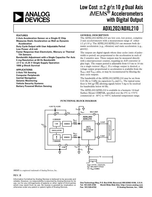
ADXL202/210 data sheet
ADXL202/210 data sheet
ADXL202/210 data sheet

Create successful ePaper yourself
Turn your PDF publications into a flip-book with our unique Google optimized e-Paper software.
a<br />
FEATURES<br />
2-Axis Acceleration Sensor on a Single IC Chip<br />
Measures Static Acceleration as Well as Dynamic<br />
Acceleration<br />
Duty Cycle Output with User Adjustable Period<br />
Low Power
<strong>ADXL202</strong>/ADXL<strong>210</strong>–SPECIFICATIONS<br />
<strong>ADXL202</strong>/JQC/AQC ADXL<strong>210</strong>/JQC/AQC<br />
Parameter Conditions Min Typ Max Min Typ Max Units<br />
SENSOR INPUT Each Axis<br />
Measurement Range1 ±1.5 ±2 ±8 ±10 g<br />
Nonlinearity Best Fit Straight Line 0.2 0.2 % of FS<br />
Alignment Error2 ±1 ±1 Degrees<br />
Alignment Error X Sensor to Y Sensor ±0.01 ±0.01 Degrees<br />
Transverse Sensitivity3 ±2 ±2 %<br />
SENSITIVITY Each Axis<br />
Duty Cycle per g T1/T2 @ +25°C 10 12.5 15 3.2 4.0 4.8 %/g<br />
Sensitivity, Analog Output At Pins XFILT, YFILT 312 100 mV/g<br />
Temperature Drift4 Δ from +25°C ±0.5 ±0.5 % Rdg<br />
ZERO g BIAS LEVEL Each Axis<br />
0 g Duty Cycle T1/T2 25 50 75 42 50 58 %<br />
Initial Offset ±2 ±2 g<br />
0 g Duty Cycle vs. Supply 1.0 4.0 1.0 4.0 %/V<br />
0 g Offset vs. Temperature4 NOISE PERFORMANCE<br />
Δ from +25°C 2.0 2.0 mg/°C<br />
Noise Density5 FREQUENCY RESPONSE<br />
@ +25°C 500 1000 500 1000 μg/√Hz<br />
3 dB Bandwidth Duty Cycle Output 500 500 Hz<br />
3 dB Bandwidth At Pins XFILT, YFILT 5 5 kHz<br />
Sensor Resonant Frequency<br />
FILTER<br />
10 14 kHz<br />
RFILT Tolerance 32 kΩ Nominal ±15 ±15 %<br />
Minimum Capacitance<br />
SELF TEST<br />
At XFILT, YFILT 1000 1000 pF<br />
Duty Cycle Change<br />
DUTY CYCLE OUTPUT STAGE<br />
Self-Test “0” to “1” 10 10 %<br />
FSET 125 MΩ/RSET 125 MΩ/RSET FSET Tolerance RSET = 125 kΩ 0.7 1.3 0.7 1.3 kHz<br />
Output High Voltage I = 25 μA VS – 200 mV VS – 200 mV mV<br />
Output Low Voltage I = 25 μA 200 200 mV<br />
T2 Drift vs. Temperature 35 35 ppm/°C<br />
Rise/Fall Time<br />
POWER SUPPLY<br />
200 200 ns<br />
Operating Voltage Range 3.0 5.25 2.7 5.25 V<br />
Specified Performance 4.75 5.25 4.75 5.25 V<br />
Quiescent Supply Current 0.6 1.0 0.6 1.0 mA<br />
Turn-On Time6 TEMPERATURE RANGE<br />
To 99% 160 CFILT + 0.3 160 CFILT + 0.3 ms<br />
Operating Range JQC 0 +70 0 +70 °C<br />
Specified Performance AQC –40 +85 –40 +85 °C<br />
NOTES<br />
1For all combinations of offset and sensitivity variation.<br />
2Alignment error is specified as the angle between the true and indicated axis of sensitivity.<br />
3Transverse sensitivity is the algebraic sum of the alignment and the inherent sensitivity errors.<br />
4Specification refers to the maximum change in parameter from its initial at +25 °C to its worst case value at TMIN to TMAX. 5Noise density (μg/√Hz) is the average noise at any frequency in the bandwidth of the part.<br />
6CFILT in μF. Addition of filter capacitor will increase turn on time. Please see the Application section on power cycling.<br />
All min and max specifications are guaranteed. Typical specifications are not tested or guaranteed.<br />
Specifications subject to change without notice.<br />
–2–<br />
(TA = TMIN to TMAX, TA = +25C for J Grade only, VDD = +5 V,<br />
RSET = 125 k, Acceleration = 0 g, unless otherwise noted)<br />
REV. B
ABSOLUTE MAXIMUM RATINGS*<br />
Acceleration (Any Axis, Unpowered for 0.5 ms) . . . . . . 1000 g<br />
Acceleration (Any Axis, Powered for 0.5 ms) . . . . . . . . . 500 g<br />
+VS . . . . . . . . . . . . . . . . . . . . . . . . . . . . . . . . –0.3 V to +7.0 V<br />
Output Short Circuit Duration<br />
(Any Pin to Common) . . . . . . . . . . . . . . . . . . . . . . Indefinite<br />
Operating Temperature . . . . . . . . . . . . . . . . . –55°C to +125°C<br />
Storage Temperature . . . . . . . . . . . . . . . . . . . –65°C to +150°C<br />
*Stresses above those listed under Absolute Maximum Ratings may cause permanent<br />
damage to the device. This is a stress rating only; the functional operation of<br />
the device at these or any other conditions above those indicated in the operational<br />
sections of this specification is not implied. Exposure to absolute maximum rating<br />
conditions for extended periods may affect device reliability.<br />
Drops onto hard surfaces can cause shocks of greater than 1000 g<br />
and exceed the absolute maximum rating of the device. Care<br />
should be exercised in handling to avoid damage.<br />
REV. B<br />
PIN FUNCTION DESCRIPTIONS<br />
Pin Name Description<br />
1 NC No Connect<br />
2 VTP Test Point, Do Not Connect<br />
3 ST Self Test<br />
4 COM Common<br />
5 T2 Connect RSET to Set T2 Period<br />
6 NC No Connect<br />
7 COM Common<br />
8 NC No Connect<br />
9 YOUT Y Axis Duty Cycle Output<br />
10 XOUT X Axis Duty Cycle Output<br />
11 YFILT Connect Capacitor for Y Filter<br />
12 XFILT Connect Capacitor for X Filter<br />
13 VDD +3 V to +5.25 V, Connect to 14<br />
14 VDD +3 V to +5.25 V, Connect to 13<br />
PACKAGE CHARACTERISTICS<br />
Package JA JC Device Weight<br />
14-Lead CERPAK 110°C/W 30°C/W 5 Grams<br />
CAUTION<br />
ESD (electrostatic discharge) sensitive device. Electrostatic charges as high as 4000 V readily<br />
accumulate on the human body and test equipment and can discharge without detection.<br />
Although the <strong>ADXL202</strong>/ADXL<strong>210</strong> features proprietary ESD protection circuitry, permanent<br />
damage may occur on devices subjected to high energy electrostatic discharges. Therefore, proper<br />
ESD precautions are recommended to avoid performance degradation or loss of functionality.<br />
–3–<br />
<strong>ADXL202</strong>/ADXL<strong>210</strong><br />
PIN CONFIGURATION<br />
NC 1<br />
14 VDD VTP ST<br />
2<br />
3<br />
<strong>ADXL202</strong>/ 13<br />
ADXL<strong>210</strong><br />
12<br />
TOP VIEW<br />
VDD XFILT COM 4 (Not to Scale) 11 YFILT T2 5<br />
AX 10 XOUT NC 6<br />
9 YOUT COM 7 AY 8 NC<br />
NC = NO CONNECT<br />
Figure 1 shows the response of the <strong>ADXL202</strong> to the Earth’s<br />
gravitational field. The output values shown are nominal. They<br />
are presented to show the user what type of response to expect<br />
from each of the output pins due to changes in orientation with<br />
respect to the Earth. The ADXL<strong>210</strong> reacts similarly with output<br />
changes appropriate to its scale.<br />
TYPICAL OUTPUT AT PIN:<br />
9 = 37.5% DUTY CYCLE<br />
10 = 50% DUTY CYCLE<br />
11 = 2.812V<br />
12 = 2.5V<br />
ORDERING GUIDE<br />
TYPICAL OUTPUT AT PIN:<br />
9 = 50% DUTY CYCLE<br />
10 = 62.5% DUTY CYCLE<br />
11 = 2.5V<br />
12 = 2.188V<br />
TYPICAL OUTPUT AT PIN:<br />
9 = 50% DUTY CYCLE<br />
10 = 37.5% DUTY CYCLE<br />
11 = 2.5V<br />
12 = 2.812V<br />
TYPICAL OUTPUT AT PIN:<br />
9 = 62.5% DUTY CYCLE<br />
10 = 50% DUTY CYCLE<br />
11 = 2.188V<br />
12 = 2.5V<br />
1g<br />
EARTH'S SURFACE<br />
Figure 1. <strong>ADXL202</strong>/ADXL<strong>210</strong> Nominal Response Due to<br />
Gravity<br />
g Temperature Package Package<br />
Model Range Range Description Option<br />
<strong>ADXL202</strong>JQC ± 2 0°C to +70°C 14-Lead CERPAK QC-14<br />
<strong>ADXL202</strong>AQC ± 2 –40°C to +85°C 14-Lead CERPAK QC-14<br />
ADXL<strong>210</strong>JQC ± 10 0°C to +70°C 14-Lead CERPAK QC-14<br />
ADXL<strong>210</strong>AQC ± 10 –40°C to +85°C 14-Lead CERPAK QC-14<br />
WARNING!<br />
ESD SENSITIVE DEVICE
<strong>ADXL202</strong>/ADXL<strong>210</strong><br />
TYPICAL CHARACTERISTICS<br />
PERIOD NORMALIZED TO 1 AT 25 C<br />
1.06<br />
1.04<br />
1.02<br />
1.00<br />
0.98<br />
0.96<br />
0.94<br />
–45 –30 –15 0 15 30 45 60 75 90<br />
TEMPERATURE – C<br />
Figure 2. Normalized DCM Period (T2) vs. Temperature<br />
ZERO g OFFSET SHIFT IN g<br />
0.8<br />
0.6<br />
0.4<br />
0.2<br />
0<br />
–0.2<br />
–0.4<br />
–0.6<br />
–0.8<br />
–40 –30 –20 –10 0 10 20 30 40 50 60 70 80 90<br />
TEMPERATURE – C<br />
Figure 3. Typical Zero g Offset vs. Temperature<br />
SUPPLY CURRENT – mA<br />
0.7<br />
0.6<br />
0.5<br />
0.4<br />
0.3<br />
0.2<br />
0.1<br />
V S = 5 VDC<br />
V S = 3.5 VDC<br />
0<br />
–40 –20 0 20 40 60 80 100<br />
TEMPERATURE – C<br />
Figure 4. Typical Supply Current vs. Temperature<br />
(@ +25C RSET = 125 k, VDD = +5 V, unless otherwise noted)<br />
–4–<br />
CHANGE IN SENSITIVITY<br />
4%<br />
3%<br />
2%<br />
1%<br />
0%<br />
–1%<br />
–2%<br />
–3%<br />
–4%<br />
–40 25<br />
TEMPERATURE – C<br />
85<br />
Figure 5. Typical X Axis Sensitivity Drift Due to<br />
Temperature<br />
VOLTS<br />
PERCENTAGE OF SAMPLES<br />
3<br />
2<br />
1<br />
0<br />
20<br />
18<br />
16<br />
14<br />
12<br />
10<br />
8<br />
6<br />
4<br />
2<br />
0<br />
–0.87g<br />
C FILT = 0.01F<br />
0 0.4 0.8<br />
FREQUENCY – ms<br />
1.2 1.4<br />
Figure 6. Typical Turn-On Time<br />
–0.64g –0.41g –0.17g 0.06g 0.29g 0.52g 0.75g<br />
g/DUTY CYCLE OUTPUT<br />
Figure 7. Typical Zero g Distribution at +25°C<br />
REV. B
TOTAL RMS NOISE – mg<br />
PERCENTAGE OF SAMPLES<br />
REV. B<br />
9<br />
8<br />
7<br />
6<br />
5<br />
4<br />
3<br />
2<br />
1<br />
0<br />
11.3 11.5 11.7 11.9 12.2 12.4 12.6 12.8 13.1 13.3 13.5 13.7<br />
DUTY CYCLE OUTPUT – % per g<br />
14<br />
12<br />
10<br />
Figure 8. Typical Sensitivity per g at +25°C<br />
8<br />
6<br />
4<br />
2<br />
0<br />
0.01F<br />
500Hz<br />
0.047F<br />
100Hz<br />
C X , C Y<br />
BANDWIDTH<br />
0.1F<br />
50Hz<br />
Figure 9. Typical Noise at XFILT Output<br />
0.47F<br />
10Hz<br />
–5–<br />
TOTAL RMS NOISE – mg<br />
% OF PARTS<br />
14<br />
12<br />
10<br />
8<br />
6<br />
4<br />
2<br />
C FILT = 0.01F<br />
BW = 500Hz<br />
<strong>ADXL202</strong>/ADXL<strong>210</strong><br />
C FILT = 0.047F<br />
BW = 100Hz<br />
C FILT = 0.1F<br />
BW = 50Hz<br />
T2 = 1ms<br />
C FILT = 0.47F<br />
BW = 10Hz<br />
0<br />
1 4<br />
16<br />
64<br />
NUMBER OF AVERAGE SAMPLES<br />
Figure 10. Typical Noise at Digital Outputs<br />
20<br />
18<br />
16<br />
14<br />
12<br />
10<br />
8<br />
6<br />
4<br />
2<br />
0<br />
–1.375<br />
–1.125<br />
–0.875<br />
–0.625<br />
–0.375<br />
–0.0125<br />
0.0125<br />
0.375<br />
0.625<br />
DEGREES OF MISALIGNMENT<br />
0.875<br />
1.125<br />
Figure 11. Rotational Die Alignment<br />
1.375
<strong>ADXL202</strong>/ADXL<strong>210</strong><br />
DEFINITIONS<br />
T1 Length of the “on” portion of the cycle.<br />
T2 Length of the total cycle.<br />
Duty Cycle Ratio of the “on” time (T1) of the cycle to the total<br />
cycle (T2). Defined as T1/T2 for the <strong>ADXL202</strong>/<br />
ADXL<strong>210</strong>.<br />
Pulsewidth Time period of the “on” pulse. Defined as T1 for<br />
the <strong>ADXL202</strong>/ADXL<strong>210</strong>.<br />
THEORY OF OPERATION<br />
The <strong>ADXL202</strong>/ADXL<strong>210</strong> are complete dual axis acceleration<br />
measurement systems on a single monolithic IC. They contain a<br />
polysilicon surface-micromachined sensor and signal conditioning<br />
circuitry to implement an open loop acceleration measurement<br />
architecture. For each axis, an output circuit converts the<br />
analog signal to a duty cycle modulated (DCM) digital signal<br />
that can be decoded with a counter/timer port on a microprocessor.<br />
The <strong>ADXL202</strong>/ADXL<strong>210</strong> are capable of measuring<br />
both positive and negative accelerations to a maximum level of<br />
± 2 g or ± 10 g. The accelerometer measures static acceleration<br />
forces such as gravity, allowing it to be used as a tilt sensor.<br />
The sensor is a surface micromachined polysilicon structure<br />
built on top of the silicon wafer. Polysilicon springs suspend the<br />
structure over the surface of the wafer and provide a resistance<br />
against acceleration forces. Deflection of the structure is measured<br />
using a differential capacitor that consists of independent<br />
fixed plates and central plates attached to the moving mass. The<br />
fixed plates are driven by 180° out of phase square waves. An<br />
acceleration will deflect the beam and unbalance the differential<br />
capacitor, resulting in an output square wave whose amplitude<br />
is proportional to acceleration. Phase sensitive demodulation<br />
techniques are then used to rectify the signal and determine the<br />
direction of the acceleration.<br />
The output of the demodulator drives a duty cycle modulator<br />
(DCM) stage through a 32 kΩ resistor. At this point a pin is<br />
available on each channel to allow the user to set the signal<br />
bandwidth of the device by adding a capacitor. This filtering<br />
improves measurement resolution and helps prevent aliasing.<br />
After being low-pass filtered, the analog signal is converted to a<br />
duty cycle modulated signal by the DCM stage. A single resistor<br />
sets the period for a complete cycle (T2), which can be set between<br />
0.5 ms and 10 ms (see Figure 12). A 0 g acceleration<br />
produces a nominally 50% duty cycle. The acceleration signal<br />
can be determined by measuring the length of the T1 and T2<br />
pulses with a counter/timer or with a polling loop using a low<br />
cost microcontroller.<br />
An analog output voltage can be obtained either by buffering the<br />
signal from the XFILT and YFILT pin, or by passing the duty cycle<br />
signal through an RC filter to reconstruct the dc value.<br />
The <strong>ADXL202</strong>/ADXL<strong>210</strong> will operate with supply voltages as<br />
low as 3.0 V or as high as 5.25 V.<br />
T1<br />
T2<br />
A(g) = (T1/T2 – 0.5)/12.5%<br />
0g = 50% DUTY CYCLE<br />
T2(s) = R SET ()/125M<br />
Figure 12. Typical Output Duty Cycle<br />
–6–<br />
APPLICATIONS<br />
POWER SUPPLY DECOUPLING<br />
For most applications a single 0.1 μF capacitor, CDC, will adequately<br />
decouple the accelerometer from signal and noise on<br />
the power supply. However, in some cases, especially where digital<br />
devices such as microcontrollers share the same power supply, digital<br />
noise on the supply may cause interference on the <strong>ADXL202</strong>/<br />
ADXL<strong>210</strong> output. This is often observed as a slowly undulating<br />
fluctuation of voltage at XFILT and YFILT. If additional decoupling<br />
is needed, a 100 Ω (or smaller) resistor or ferrite beads,<br />
may be inserted in the <strong>ADXL202</strong>/ADXL<strong>210</strong>’s supply line.<br />
DESIGN PROCEDURE FOR THE <strong>ADXL202</strong>/ADXL<strong>210</strong><br />
The design procedure for using the <strong>ADXL202</strong>/ADXL<strong>210</strong> with a<br />
duty cycle output involves selecting a duty cycle period and a<br />
filter capacitor. A proper design will take into account the application<br />
requirements for bandwidth, signal resolution and acquisition<br />
time, as discussed in the following sections.<br />
V DD<br />
The <strong>ADXL202</strong>/ADXL<strong>210</strong> have two power supply (VDD) Pins:<br />
13 and 14. These two pins should be connected directly together.<br />
COM<br />
The <strong>ADXL202</strong>/ADXL<strong>210</strong> have two commons, Pins 4 and 7.<br />
These two pins should be connected directly together and Pin 7<br />
grounded.<br />
VTP This pin is to be left open; make no connections of any kind to<br />
this pin.<br />
Decoupling Capacitor CDC A 0.1 μF capacitor is recommended from VDD to COM for<br />
power supply decoupling.<br />
ST<br />
The ST pin controls the self-test feature. When this pin is set to<br />
VDD, an electrostatic force is exerted on the beam of the accelerometer.<br />
The resulting movement of the beam allows the user to<br />
test if the accelerometer is functional. The typical change in<br />
output will be 10% at the duty cycle outputs (corresponding to<br />
800 mg). This pin may be left open circuit or connected to<br />
common in normal use.<br />
Duty Cycle Decoding<br />
The <strong>ADXL202</strong>/ADXL<strong>210</strong>’s digital output is a duty cycle modulator.<br />
Acceleration is proportional to the ratio T1/T2. The<br />
nominal output of the <strong>ADXL202</strong> is:<br />
0 g = 50% Duty Cycle<br />
Scale factor is 12.5% Duty Cycle Change per g<br />
The nominal output of the ADXL<strong>210</strong> is:<br />
0 g = 50% Duty Cycle<br />
Scale factor is 4% Duty Cycle Change per g<br />
These nominal values are affected by the initial tolerance of the<br />
device including zero g offset error and sensitivity error.<br />
T2 does not have to be measured for every measurement cycle.<br />
It need only be updated to account for changes due to temperature,<br />
(a relatively slow process). Since the T2 time period is<br />
shared by both X and Y channels, it is necessary only to measure<br />
it on one channel of the <strong>ADXL202</strong>/ADXL<strong>210</strong>. Decoding<br />
algorithms for various microcontrollers have been developed.<br />
Consult the appropriate Application Note.<br />
REV. B
Setting the Bandwidth Using C X and C Y<br />
The <strong>ADXL202</strong>/ADXL<strong>210</strong> have provisions for bandlimiting the<br />
XFILT and YFILT pins. Capacitors must be added at these pins to<br />
implement low-pass filtering for antialiasing and noise reduction.<br />
The equation for the 3 dB bandwidth is:<br />
or, more simply,<br />
REV. B<br />
C DC<br />
F –3 dB =<br />
F –3 dB =<br />
+3.0V TO +5.25V<br />
VDD<br />
X SENSOR<br />
OSCILLATOR<br />
Y SENSOR<br />
1<br />
2 π (32 kΩ) × C(x, y)<br />
( )<br />
5 μF<br />
C (X ,Y )<br />
COM<br />
DEMOD<br />
The tolerance of the internal resistor (RFILT), can vary as much<br />
as ± 25% of its nominal value of 32 kΩ; so the bandwidth will<br />
vary accordingly. A minimum capacitance of 1000 pF for C(X, Y)<br />
is required in all cases.<br />
Table I. Filter Capacitor Selection, C X and C Y<br />
Bandwidth<br />
Capacitor<br />
Value<br />
10 Hz 0.47 μF<br />
50 Hz 0.10 μF<br />
100 Hz 0.05 μF<br />
200 Hz 0.027 μF<br />
500 Hz 0.01 μF<br />
5 kHz 0.001 μF<br />
Setting the DCM Period with R SET<br />
The period of the DCM output is set for both channels by a<br />
single resistor from RSET to ground. The equation for the period<br />
is:<br />
T2 = RSET (Ω)<br />
125 MΩ<br />
R FILT<br />
32k<br />
R FILT<br />
32k<br />
A 125 kΩ resistor will set the duty cycle repetition rate to approximately<br />
1 kHz, or 1 ms. The device is designed to operate at<br />
duty cycle periods between 0.5 ms and 10 ms.<br />
VDD<br />
DEMOD<br />
C X<br />
Y FILT<br />
X FILT<br />
<strong>ADXL202</strong>/<br />
ADXL<strong>210</strong><br />
C Y<br />
SELF TEST<br />
DUTY<br />
CYCLE<br />
MODULATOR<br />
(DCM)<br />
T2<br />
R SET<br />
–7–<br />
X OUT<br />
Y OUT<br />
C<br />
O<br />
U<br />
N<br />
T<br />
E<br />
R<br />
Figure 13. Block Diagram<br />
P<br />
T1<br />
<strong>ADXL202</strong>/ADXL<strong>210</strong><br />
Table II. Resistor Values to Set T2<br />
T2 RSET<br />
1 ms 125 kΩ<br />
2 ms 250 kΩ<br />
5 ms 625 kΩ<br />
10 ms 1.25 MΩ<br />
Note that the RSET should always be included, even if only an<br />
analog output is desired. Use an RSET value between 500 kΩ<br />
and 2 MΩ when taking the output from XFILT or YFILT. The<br />
RSET resistor should be place close to the T2 Pin to minimize<br />
parasitic capacitance at this node.<br />
Selecting the Right Accelerometer<br />
For most tilt sensing applications the <strong>ADXL202</strong> is the most<br />
appropriate accelerometer. Its higher sensitivity (12.5%/g allows<br />
the user to use a lower speed counter for PWM decoding while<br />
maintaining high resolution. The ADXL<strong>210</strong> should be used in<br />
applications where accelerations of greater than ±2 g are expected.<br />
MICROCOMPUTER INTERFACES<br />
The <strong>ADXL202</strong>/ADXL<strong>210</strong> were specifically designed to work<br />
with low cost microcontrollers. Specific code sets, reference<br />
designs, and application notes are available from the factory.<br />
This section will outline a general design procedure and discuss<br />
the various trade-offs that need to be considered.<br />
The designer should have some idea of the required performance<br />
of the system in terms of:<br />
Resolution: the smallest signal change that needs to be detected.<br />
Bandwidth: the highest frequency that needs to be detected.<br />
Acquisition Time: the time that will be available to acquire the<br />
signal on each axis.<br />
These requirements will help to determine the accelerometer<br />
bandwidth, the speed of the microcontroller clock and the<br />
length of the T2 period.<br />
When selecting a microcontroller it is helpful to have a counter<br />
timer port available. The microcontroller should have provisions<br />
for software calibration. While the <strong>ADXL202</strong>/ADXL<strong>210</strong> are<br />
highly accurate accelerometers, they have a wide tolerance for<br />
T2<br />
A(g) = (T1/T2 – 0.5)/12.5%<br />
0g = 50% DUTY CYCLE<br />
T2 = RSET /125M
<strong>ADXL202</strong>/ADXL<strong>210</strong><br />
initial offset. The easiest way to null this offset is with a calibration<br />
factor saved on the microcontroller or by a user calibration<br />
for zero g. In the case where the offset is calibrated during manufacture,<br />
there are several options, including external EEPROM<br />
and microcontrollers with “one-time programmable” features.<br />
DESIGN TRADE-OFFS FOR SELECTING FILTER<br />
CHARACTERISTICS: THE NOISE/BW TRADE-OFF<br />
The accelerometer bandwidth selected will determine the measurement<br />
resolution (smallest detectable acceleration). Filtering<br />
can be used to lower the noise floor and improve the resolution<br />
of the accelerometer. Resolution is dependent on both the analog<br />
filter bandwidth at XFILT and YFILT and on the speed of the<br />
microcontroller counter.<br />
The analog output of the <strong>ADXL202</strong>/ADXL<strong>210</strong> has a typical<br />
bandwidth of 5 kHz, much higher than the duty cycle stage is<br />
capable of converting. The user must filter the signal at this<br />
point to limit aliasing errors. To minimize DCM errors the<br />
analog bandwidth should be less than 1/10 the DCM frequency.<br />
Analog bandwidth may be increased to up to 1/2 the DCM<br />
frequency in many applications. This will result in greater dynamic<br />
error generated at the DCM.<br />
The analog bandwidth may be further decreased to reduce noise<br />
and improve resolution. The <strong>ADXL202</strong>/ADXL<strong>210</strong> noise has<br />
the characteristics of white Gaussian noise that contributes<br />
equally at all frequencies and is described in terms of μg per root<br />
Hz; i.e., the noise is proportional to the square root of the bandwidth<br />
of the accelerometer. It is recommended that the user limit<br />
bandwidth to the lowest frequency needed by the application, to<br />
maximize the resolution and dynamic range of the accelerometer.<br />
With the single pole roll-off characteristic, the typical noise of<br />
the <strong>ADXL202</strong>/ADXL<strong>210</strong> is determined by the following equation:<br />
Noise ( rms)=<br />
⎛<br />
⎝<br />
500 μg/ Hz ⎞<br />
⎠<br />
At 100 Hz the noise will be:<br />
× ⎛<br />
⎝<br />
BW ×1.5 ⎞<br />
⎠<br />
Noise ( rms)=<br />
⎛<br />
⎝<br />
500 μg/ Hz ⎞<br />
⎠<br />
× ⎛<br />
⎝<br />
100 × (1.5) ⎞<br />
⎠<br />
= 6.12 mg<br />
Often the peak value of the noise is desired. Peak-to-peak noise<br />
can only be estimated by statistical methods. Table III is useful<br />
for estimating the probabilities of exceeding various peak values,<br />
given the rms value.<br />
Table III. Estimation of Peak-to-Peak Noise<br />
Nominal Peak-to-Peak<br />
% of Time that Noise<br />
Will Exceed Nominal<br />
Value Peak-to-Peak Value<br />
2.0 × rms 32%<br />
4.0 × rms 4.6%<br />
6.0 × rms 0.27%<br />
8.0 × rms 0.006%<br />
The peak-to-peak noise value will give the best estimate of the<br />
uncertainty in a single measurement.<br />
–8–<br />
Table IV gives typical noise output of the <strong>ADXL202</strong>/ADXL<strong>210</strong><br />
for various CX and CY values.<br />
Table IV. Filter Capacitor Selection, C X and C Y<br />
Peak-to-Peak Noise<br />
Estimate 95%<br />
Bandwidth CX, CY rms Noise Probability (rms 4)<br />
10 Hz 0.47 μF 1.9 mg 7.6 mg<br />
50 Hz 0.10 μF 4.3 mg 17.2 mg<br />
100 Hz 0.05 μF 6.1 mg 24.4 mg<br />
200 Hz 0.027 μF 8.7 mg 35.8 mg<br />
500 Hz 0.01 μF 13.7 mg 54.8 mg<br />
CHOOSING T2 AND COUNTER FREQUENCY: DESIGN<br />
TRADE-OFFS<br />
The noise level is one determinant of accelerometer resolution.<br />
The second relates to the measurement resolution of the<br />
counter when decoding the duty cycle output.<br />
The <strong>ADXL202</strong>/ADXL<strong>210</strong>’s duty cycle converter has a resolution<br />
of approximately 14 bits; better resolution than the accelerometer<br />
itself. The actual resolution of the acceleration signal is,<br />
however, limited by the time resolution of the counting devices<br />
used to decode the duty cycle. The faster the counter clock, the<br />
higher the resolution of the duty cycle and the shorter the T2<br />
period can be for a given resolution. The following table shows<br />
some of the trade-offs. It is important to note that this is the<br />
resolution due to the microprocessors’s counter. It is probable<br />
that the accelerometer’s noise floor may set the lower limit on<br />
the resolution, as discussed in the previous section.<br />
Table V. Trade-Offs Between Microcontroller Counter Rate,<br />
T2 Period and Resolution of Duty Cycle Modulator<br />
<strong>ADXL202</strong>/ Counter-<br />
ADXL<strong>210</strong> Clock Counts<br />
R SET Sample Rate per T2 Counts Resolution<br />
T2 (ms) (k) Rate (MHz) Cycle per g (mg)<br />
1.0 124 1000 2.0 2000 250 4.0<br />
1.0 124 1000 1.0 1000 125 8.0<br />
1.0 124 1000 0.5 500 62.5 16.0<br />
5.0 625 200 2.0 10000 1250 0.8<br />
5.0 625 200 1.0 5000 625 1.6<br />
5.0 625 200 0.5 2500 312.5 3.2<br />
10.0 1250 100 2.0 20000 2500 0.4<br />
10.0 1250 100 1.0 10000 1250 0.8<br />
10.0 1250 100 0.5 5000 625 1.6<br />
REV. B
STRATEGIES FOR USING THE DUTY CYCLE OUTPUT<br />
WITH MICROCONTROLLERS<br />
Application notes outlining various strategies for using the duty<br />
cycle output with low cost microcontrollers are available from<br />
the factory.<br />
USING THE <strong>ADXL202</strong>/ADXL<strong>210</strong> AS A DUAL AXIS TILT<br />
SENSOR<br />
One of the most popular applications of the <strong>ADXL202</strong>/ADXL<strong>210</strong><br />
is tilt measurement. An accelerometer uses the force of gravity<br />
as an input vector to determine orientation of an object in space.<br />
An accelerometer is most sensitive to tilt when its sensitive axis<br />
is perpendicular to the force of gravity, i.e., parallel to the<br />
earth’s surface. At this orientation its sensitivity to changes in<br />
tilt is highest. When the accelerometer is oriented on axis to<br />
gravity, i.e., near its +1 g or –1 g reading, the change in output<br />
acceleration per degree of tilt is negligible. When the accelerometer<br />
is perpendicular to gravity, its output will change nearly<br />
17.5 mg per degree of tilt, but at 45° degrees it is changing only<br />
at 12.2 mg per degree and resolution declines. The following<br />
table illustrates the changes in the X and Y axes as the device is<br />
tilted ± 90° through gravity.<br />
REV. B<br />
Y<br />
X<br />
X OUTPUT Y OUTPUT (g)<br />
X AXIS PER PER<br />
ORIENTATION DEGREE OF DEGREE OF<br />
TO HORIZON () X OUTPUT (g) TILT (mg) Y OUTPUT (g) TILT (mg)<br />
+90<br />
–90<br />
–90 –1.000 –0.2 0.000 17.5<br />
–75 –0.966 4.4 0.259 16.9<br />
–60 –0.866 8.6 0.500 15.2<br />
–45 –0.707 12.2 0.707 12.4<br />
–30 –0.500 15.0 0.866 8.9<br />
–15 –0.259 16.8 0.966 4.7<br />
– 0 0.000 17.5 1.000 0.2<br />
– 15 0.259 16.9 0.966 –4.4<br />
– 30 0.500 15.2 0.866 –8.6<br />
– 45 0.707 12.4 0.707 –12.2<br />
– 60 0.866 8.9 0.500 –15.0<br />
– 75 0.966 4.7 0.259 –16.8<br />
– 90 1.000 0.2 0.000 –17.5<br />
Figure 14. How the X and Y Axes Respond to Changes in<br />
Tilt<br />
0<br />
1g<br />
–9–<br />
<strong>ADXL202</strong>/ADXL<strong>210</strong><br />
A DUAL AXIS TILT SENSOR: CONVERTING<br />
ACCELERATION TO TILT<br />
When the accelerometer is oriented so both its X and Y axes are<br />
parallel to the earth’s surface it can be used as a two axis tilt<br />
sensor with a roll and a pitch axis. Once the output signal from<br />
the accelerometer has been converted to an acceleration that<br />
varies between –1 g and +1 g, the output tilt in degrees is calculated<br />
as follows:<br />
Pitch = ASIN (Ax/1 g)<br />
Roll = ASIN (Ay/1 g)<br />
Be sure to account for overranges. It is possible for the accelerometers<br />
to output a signal greater than ± 1 g due to vibration,<br />
shock or other accelerations.<br />
MEASURING 360 OF TILT<br />
It is possible to measure a full 360° of orientation through gravity<br />
by using two accelerometers oriented perpendicular to one<br />
another (see Figure 15). When one sensor is reading a maximum<br />
change in output per degree, the other is at its minimum.<br />
Y<br />
X<br />
360 OF TILT 1g<br />
Figure 15. Using a Two-Axis Accelerometer to Measure<br />
360° of Tilt
<strong>ADXL202</strong>/ADXL<strong>210</strong><br />
USING THE ANALOG OUTPUT<br />
The <strong>ADXL202</strong>/ADXL<strong>210</strong> was specifically designed for use with<br />
its digital outputs, but has provisions to provide analog outputs<br />
as well.<br />
Duty Cycle Filtering<br />
An analog output can be reconstructed by filtering the duty<br />
cycle output. This technique requires only passive components.<br />
The duty cycle period (T2) should be set to 1 ms. An RC filter<br />
with a 3 dB point at least a factor of 10 less than the duty cycle<br />
frequency is connected to the duty cycle output. The filter resistor<br />
should be no less than 100 kΩ to prevent loading of the<br />
output stage. The analog output signal will be ratiometric to the<br />
supply voltage. The advantage of this method is an output scale<br />
factor of approximately double the analog output. Its disadvantage<br />
is that the frequency response will be lower than when<br />
using the XFILT, YFILT output.<br />
XFILT, YFILT Output<br />
The second method is to use the analog output present at the<br />
XFILT and YFILT pin. Unfortunately, these pins have a 32 kΩ<br />
output impedance and are not designed to drive a load directly.<br />
An op amp follower may be required to buffer this pin. The<br />
advantage of this method is that the full 5 kHz bandwidth of the<br />
accelerometer is available to the user. A capacitor still must be<br />
added at this point for filtering. The duty cycle converter should<br />
be kept running by using RSET
REV. B<br />
0.291 (7.391)<br />
0.285 (7.239)<br />
PIN 1<br />
0.020 (0.508)<br />
0.004 (0.102)<br />
SEATING<br />
PLANE<br />
OUTLINE DIMENSIONS<br />
Dimensions shown in inches and (mm).<br />
0.390 (9.906)<br />
MAX<br />
14 8<br />
1<br />
0.300 (7.62)<br />
0.050<br />
(1.27)<br />
BSC<br />
14-Lead CERPAK<br />
(QC-14)<br />
7<br />
0.419 (10.643)<br />
0.394 (10.008)<br />
0.195 (4.953)<br />
0.115 (2.921)<br />
0.020 (0.508)<br />
0.013 (0.330)<br />
0.215 (5.461)<br />
0.119 (3.023)<br />
–11–<br />
0.0125 (0.318)<br />
0.009 (0.229)<br />
0.345 (8.763)<br />
0.290 (7.366)<br />
8°<br />
0°<br />
0.050 (1.270)<br />
0.016 (0.406)<br />
<strong>ADXL202</strong>/ADXL<strong>210</strong><br />
C3037b–2–4/99<br />
PRINTED IN U.S.A.