ABSTRACT 1.pdf - Dyuthi Home - Cochin University of Science and ...
ABSTRACT 1.pdf - Dyuthi Home - Cochin University of Science and ...
ABSTRACT 1.pdf - Dyuthi Home - Cochin University of Science and ...

Create successful ePaper yourself
Turn your PDF publications into a flip-book with our unique Google optimized e-Paper software.
<strong>ABSTRACT</strong><br />
Thermopower <strong>and</strong> electrical conductivity studies in the transparent<br />
conducting oxide Sn doped MgIn2O4<br />
Krishnendu Biswas <strong>and</strong> U. V. Varadaraju*<br />
Materials <strong>Science</strong> Research Centre <strong>and</strong> Department <strong>of</strong> Chemistry,<br />
Indian Institute <strong>of</strong> Technology Madras, Chennai – 600 036.<br />
Email: varada@iitm.ac.in<br />
Transparent conducting oxides (TCOs) form a<br />
unique class <strong>of</strong> materials, which possess high transparency<br />
in the visible region as well as high electrical conductivity.<br />
Sn doped In2O3 (ITO) is the best known TCO with<br />
conductivities ranging from 1000 to 5000 S/cm. These<br />
find applications in LCD, photovoltaics <strong>and</strong> electrochromic<br />
devices. MgIn2O4 is known to be a TCO 1 with a b<strong>and</strong> gap<br />
<strong>of</strong> 3.4 eV. This crystallizes in the cubic system with a<br />
spinel structure. Mg2SnO4 has a inverse spinel structure<br />
<strong>and</strong> is an insulator with a large b<strong>and</strong> gap (~4.5 e.V). The<br />
aim <strong>of</strong> the present study is to induce semiconducting nature<br />
in MgIn2O4 by doping with Sn <strong>and</strong> study its optical <strong>and</strong><br />
transport properties.<br />
I INTRODUCTION<br />
Transparent conducting compounds (TCOs) are<br />
compounds which in spite being high b<strong>and</strong> gap materials,<br />
show almost metallic conductivity. Some <strong>of</strong> the binary<br />
oxides such as In2O3, SnO2 <strong>and</strong> ZnO show this type <strong>of</strong><br />
properties with electrons as the majority charge carriers.<br />
Sn doped In2O3 (ITO) is the commercially used TCO.<br />
These compounds find applications in flat panel displays,<br />
electrochromic devices etc. In 1977 Shannon et. al found<br />
that ternary oxides containing Sn or In like Cd2SnO4,<br />
CdIn2O4, In2TeO6 <strong>and</strong> CdSnO3 also show TCO properties 2 .<br />
The conductivity in these compounds are assumed due to<br />
oxygen deficiency<br />
Ueda et. al have reported MgIn2O4-x to be one <strong>of</strong><br />
the promising new TCO 2 . This crystallizes in the spinel<br />
structure with a large b<strong>and</strong> gap <strong>of</strong> 3.4 eV. The conductivity<br />
in TCOs is due to the edge sharing InO6 octahedra.<br />
Mg2SnO4 is an insulator crystallizing in an inverse spinel<br />
structure with a b<strong>and</strong> gap <strong>of</strong> ~4.5 e.V. Recently, Kammler<br />
et. al. studied phase relations, transparent <strong>and</strong> optical<br />
properties in a novel transparent conducting spinel solid<br />
solution Cd1+xIn2-2xSnxO4 3 in which both the end members<br />
viz. CdIn2O4 <strong>and</strong> Cd2SnO4 are TCOs. They reported that<br />
conductivity increased with Sn doping.<br />
In thermoelectric materials, the dimensionless<br />
figure <strong>of</strong> merit is inversely related to the thermal<br />
conductivity. It is known that structures with more<br />
disorderliness generally have greater phonon scattering<br />
effect <strong>and</strong> hence lower thermal conductivity. With this in<br />
view we have explored the thermoelectric properties <strong>of</strong> the<br />
Sn doped MgIn2O4. We have also carried out the optical<br />
<strong>and</strong> resistivity studies on the compositions to know the<br />
b<strong>and</strong> gaps <strong>and</strong> the conducting nature <strong>of</strong> the samples.<br />
II EXPERIMENTAL<br />
All the compounds were synthesized by<br />
conventional high temperature solid state reaction method.<br />
The starting materials 4MgCO3. Mg(OH)2.5H2O (A. R<br />
grade), In2O3 (Cerac 99.99%), SnO2 (cerac 99.99%) were<br />
taken in stoichiometric amounts <strong>and</strong> ground for half an<br />
hour in an agate mortar <strong>and</strong> pestle. The finely ground<br />
powders were subjected to heat treatments at 900°C 12h,<br />
1200°C 24h with intermittent grinding. The powders were<br />
palletized <strong>and</strong> sintered at 1300°C for 48h. The phase purity<br />
was checked by powder XRD patterns (CuKá1 radiation)<br />
taken on Rich Seifert P3000, German make. The diffuse<br />
reflectance spectra were taken on UV-Visible<br />
spectrophotometer (JASCO, Japan) with a 150mm<br />
integrating sphere attachment.<br />
The high temperature resistivity <strong>and</strong> thermopower<br />
measurements were done on a home built apparatus. The<br />
furnace was heated at a rate <strong>of</strong> 1C/min <strong>and</strong> a temperature<br />
gradient <strong>of</strong> 2-3K was maintained across the sample for the<br />
thermopower measurements. The resistivity measurement<br />
was done following van der Pauw four point probe method.<br />
III. RESULTS AND DISCUSSION<br />
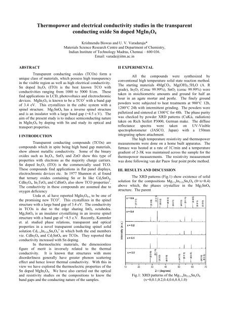
The XRD patterns (Fig.1) show existence <strong>of</strong> solid<br />
solution for the compositions Mg1+xIn2-2xSnxO4 (0
compounds with x=0, 0.1, 0.2 <strong>and</strong> 0.4 <strong>and</strong> the compound<br />
with x=0.4 are indexed on the basis <strong>of</strong> MgIn2O4 (JCPDS<br />
card no.s 73-2414) <strong>and</strong> Mg2SnO4 structures (JCPDS card<br />
no. 24-0723) respectively. Mg 2+ <strong>and</strong> Sn 4+ occupy the<br />
octahedral sites in the MgIn2O4 lattice because <strong>of</strong> their<br />
similar sizes. The lattice parameters show a decreasing<br />
trend with increasing Sn doping following Vegards law<br />
(Fig.2a). This is due to<br />
the smaller ionic radii <strong>of</strong> Sn 4+ in the octahedral<br />
coordination when compared to In 3+ ion 4 . This also<br />
confirms the incorporation <strong>of</strong> Sn 4+ in the lattice.<br />
The b<strong>and</strong> gaps measured from the diffuse<br />
reflectance spectra (Fig 2b) show an increasing trend with<br />
increasing Sn 4+ concentration in accordance with the b<strong>and</strong><br />
gaps <strong>of</strong> the end members.<br />
a) b)<br />
Fig.2 a) Lattice parameter <strong>and</strong> b) b<strong>and</strong> gap variation <strong>of</strong> the<br />
compositions (x = 0, 0.1, 0.2, 0.4, 0.6)<br />
The high temperature thermopower studies on the<br />
compositions with x=0, 0.1 <strong>and</strong> 0.2 are carried out in the<br />
temperature range 300K to 600K. The parent compound<br />
which has electrons as the major carriers show an<br />
increasing trend in the thermopower with increasing<br />
temperature (Fig.3a) which indicates its metallic nature.<br />
a) b)<br />
c)<br />
Fig. 3 High temperature thermopower plots for<br />
compositions a) x = 0, b) x = 0.1, c) x = 0.2<br />
The composition with x = 0.1 shows decreasing<br />
thermopower with increasing temperature (Fig. 3b). This<br />
shows that doping Sn 4+ makes MgIn2O4 semiconducting at<br />
x = 0.1. In case <strong>of</strong> x = 0.2 (Fig. 2c) also we find a<br />
semiconducting nature. This shows that even a small<br />
amount <strong>of</strong> Sn 4+ is sufficient to make the metallic MgIn2O4,<br />
semiconducting.<br />
The resistivity measurements are done in the<br />
temperature range 300K to 600K for the compositions x=0,<br />
0.1, 0.2. The resistivities <strong>of</strong> the samples increase with<br />
increasing Sn content (Fig. 4). This is in accordance with<br />
the b<strong>and</strong> gap increase. In all the cases the resistivity plots<br />
show a semiconducting nature. The sample with<br />
composition x = 0.4 is found to be highly insulating<br />
Fig 4. Resistivity variation with temperature for<br />
compositions a) x = 0, b) x = 0.1, c) x = 0.2<br />
The thermopower <strong>and</strong> resistivity data show that<br />
Sn doping in MgIn2O4 makes it semiconducting for x = 0.1<br />
above which, the resistivity becomes large. The parent<br />
phase has a Seebeck coefficient <strong>of</strong> -1700μV/K <strong>and</strong><br />
resistivity <strong>of</strong> 0.525Ωcm at 600K, which gives a power<br />
factor <strong>of</strong> 5.5 μW/cm.K 2 . Due to the disorder in Mg 2+ <strong>and</strong><br />
Sn 4+ in the octahedral sites, it is expected that the doped<br />
compositions have lower thermal conductivities than the<br />
parent phases <strong>and</strong> hence can result in the improvement <strong>of</strong><br />
the dimensionless figure <strong>of</strong> merit.<br />
CONCLUSION<br />
a) a)<br />
b)<br />
c)<br />
We have carried out high temperature<br />
thermopower <strong>and</strong> resistivity measurements on Sn doped<br />
MgIn2O4 for the compositions x = 0, 0.1 <strong>and</strong> 0.2. All the<br />
compositions show n-type conduction. From the<br />
thermopower data we conclude that small amount <strong>of</strong> Sn (x
= 0.1) is sufficient to bring about semiconducting property<br />
in MgIn2O4 The resistivity data show semiconducting<br />
nature for the parent phase as well as the doped<br />
compositions. The Mg 2+ <strong>and</strong> Sn 4+ ions occupy the<br />
octahedral sites. Though the resistivity comes down on<br />
doping, a cation disorder may set in which, can result in<br />
efficient phonon scattering thereby reducing the thermal<br />
conductivity <strong>of</strong> the doped compositions. In this way we<br />
expect the doped composition to have lower thermal<br />
conductivity than the parent phase<br />
REFERENCE<br />
1 R. D. Shannon, J. L. Gillson <strong>and</strong> R. J. Bouchard, J. Phys.<br />
Chem. Solids. 38, 877 (1977)<br />
2 N. Ueda, T. Omata, N. Hikuma, K. Ueda, H. Mizoguchi,<br />
T. Hashimoto <strong>and</strong> H. Kawazoe, Appl. Phys. Lett. 61(16),<br />
1954(1992)<br />
3 D. R. Kammler, T. O. Mason <strong>and</strong> K. R. Poeppelmeier,<br />
Chem. Mater. 12, 1954 (2000)<br />
4 R. D. Shannon, Acta Crystallogr. A32, 751 (1976)
Challenges in Tribological Coatings in Tubes<br />
A.Subramanyam,<br />
Indian Institue <strong>of</strong> Technology, Chennai<br />
IT02<br />
Tribology deals with wear, friction <strong>and</strong> lubrication. Where ever there are two surfaces in motion<br />
(in mechanical or in biological systems) involves friction. The Tribological coatings are gaining<br />
importance where there are atringent requirements <strong>of</strong> design parameters: like in high speed<br />
motor bearings, artificial heart impellers, satellite gyros etc. A large number <strong>of</strong> applications<br />
require the friction is to be minimized, if not eliminated. There is a special requirement <strong>of</strong> the<br />
wear <strong>and</strong> friction to be minimized in gun barrels. The wear resistance coatings also are required<br />
in oil pipes where corrosion is a serious problem. The challenge to the thin film coating<br />
community is how to deposit the wear resistance <strong>and</strong> lubricative coatings in the inner surfaces <strong>of</strong><br />
tubes. These challenges are also addressed in complicated curvatures in biological <strong>and</strong> MEMS<br />
devices. The present talk gives the basics <strong>of</strong> the coatings in general <strong>and</strong> Tribological coatings in<br />
particular on the inner surfaces <strong>of</strong> tubes. The basic principles <strong>of</strong> Magnetron coatings,<br />
thermodynamics <strong>of</strong> film formation <strong>and</strong> adhesion are also addressed.
Sorry!!<br />
This Paper is NOT Available
Ion Assisted Deposition <strong>of</strong> Sputtered Thin Films – Bias Sputtering to<br />
ECR Assisted Growth<br />
G. Mohan Rao, K. Deenamma Vargheese, S. Guruvenkat <strong>and</strong> S.K. Patra<br />
Department <strong>of</strong> Instrumentation<br />
Indian Institute <strong>of</strong> <strong>Science</strong><br />
Bangalore 560012<br />
IT04<br />
Ion assisted deposition <strong>of</strong> thin films is a popular technique to achieve good quality thin films in<br />
terms <strong>of</strong> crystallinity, micro structure <strong>and</strong> physical properties. Ion flux <strong>and</strong> Ion energy play a dominant role<br />
in the process optimization. While conventional ion guns are used in evaporation technique, their use in<br />
sputter deposition is limited due to geometrical <strong>and</strong> pressure constraints. In this paper ion assistance on the<br />
growth <strong>of</strong> thin films <strong>of</strong> silicon nitride <strong>and</strong> titanium nitride would be discussed. The ion assistance in the<br />
form <strong>of</strong> bias magnetron sputtering, unbalanced magnetron sputtering <strong>and</strong> ECR assisted deposition would be<br />
discussed. These three techniques represent different degrees <strong>of</strong> ion flux <strong>and</strong> ion density. Their effect on<br />
the microstructure evolution <strong>and</strong> properties <strong>of</strong> the deposited films would be analyzed in detail.
Planar Active Waveguide Devices on Glass-<br />
Fabrication <strong>and</strong> Characteristics<br />
Gin Jose<br />
Department <strong>of</strong> Physics, Indian Institute <strong>of</strong> Technology Guwahati,<br />
Guwahati 781039, India.<br />
E-mail: gjose@iitg.ernet.in<br />
IT05<br />
Planar integrated lightwave circuits featuring active elements are a recent addition to the modern all-optical<br />
wavelength division multiplexed (WDM) networks. Integrated amplifiers <strong>and</strong> lasers operating in the<br />
conventional b<strong>and</strong> (1530-1565nm) are by <strong>and</strong> large fabricated using erbium or erbium/ytterbium doped<br />
active glass. Technologies such as ion exchange, thin film sputtering, silica-on-silicon, sol-gel, PECVD,<br />
femtosecond laser writing were proved valid for device fabrication. In this talk a review <strong>of</strong> the development<br />
in the field will be presented. In particular, the design <strong>and</strong> fabrication <strong>of</strong> silver-sodium ion exchanged<br />
waveguides on Er-Yb phosphate glass <strong>and</strong> their lasing <strong>and</strong> amplifying properties are important. We<br />
investigated the design issues related to the dependence <strong>of</strong> ion exchange on the spectroscopic properties.<br />
Optical nonlinearities in silver diffused waveguides resulting from nanocluster formation, which are<br />
promising for all optical switching devices, will be discussed.
IT06<br />
In-situ characterization <strong>of</strong> Silicon based Thin Film growth <strong>and</strong> Interface<br />
formation by Contactless Transient Photoconductivity measurements<br />
H.C. Neitzert<br />
Department <strong>of</strong> Electrical Engineering (DIIIE)<br />
Salerno <strong>University</strong>, Fisciano - 84084, ITALY<br />
E-mail: neitzert@unisa.it<br />
A common deposition technique for thin silicon films, with industrial applications like solar cell<br />
<strong>and</strong> active matrix display production, is plasma enhanced chemical vapor deposition (PECVD). Thin film<br />
semiconductor growth is a rather complicated process <strong>and</strong> influenced by a large number <strong>of</strong> parameters.<br />
Therefore the application <strong>of</strong> in-situ measurement techniques is <strong>of</strong> great interest. There have been strong<br />
efforts to correlate the measured plasma parameters <strong>and</strong> the chemical precursor distribution in the gas phase<br />
with the deposited film properties 1 . Another possible approach for in-situ process control <strong>and</strong> parameter<br />
optimization are direct measurements <strong>of</strong> the growing film properties. In this latter case non-invasive<br />
techniques, that do not require special test structures, are certainly <strong>of</strong> great advantage. Optical techniques,<br />
like spectroscopic ellipsometry 2,3 have been shown to give detailed information regarding the film<br />
structure. Microwave reflection based techniques can be used to measure important semiconductor<br />
parameters like charge carrier mobilities <strong>and</strong> minority carrier lifetimes <strong>and</strong> are common tools for silicon<br />
wafer inspection before processing. Here we will demonstrate the capabilities <strong>of</strong> transient<br />
photoconductivity measurements, based on the microwave reflection change <strong>of</strong> semiconductor films after<br />
generation <strong>of</strong> free carriers by short laser pulses 4 , for the in-situ characterization during PECVD growth <strong>of</strong><br />
amorphous hydrogenated silicon (a-Si:H) <strong>and</strong> for the kinetics <strong>of</strong> the formation <strong>of</strong> various interfaces.<br />
The amplitude <strong>of</strong> the measured microwave reflection transients is proportional to the product <strong>of</strong><br />
the number <strong>of</strong> photo generated charge carriers multiplied with their respective mobilities. In the initial<br />
phase <strong>of</strong> the growth <strong>of</strong> a-Si:H films on glass substrates we find consequently an increasing signal<br />
amplitude, observe interference peaks <strong>and</strong> can, by comparison <strong>of</strong> the measured amplitude changes with<br />
modeling <strong>of</strong> the optical absorption, use the technique for in-situ thickness control. Even a-Si:H films with<br />
thicknesses below 3nm can be characterized regarding their electrical properties, where we still observe<br />
isl<strong>and</strong>-like growth. This means that we can get information about transport properties <strong>of</strong> films, where<br />
classical electrical measurements with contacts cannot be applied. Depositing relatively thick layers with<br />
different plasma conditions on top <strong>of</strong> each other <strong>and</strong> using short wavelengths for optical excitation, it can<br />
be shown that parameter optimization is possible in a continuous deposition sequence, without necessity <strong>of</strong><br />
preparing a large number <strong>of</strong> single thin films. Another interesting application is the determination <strong>of</strong> active<br />
dopant concentrations. This type <strong>of</strong> measurements are based either on the change <strong>of</strong> the charge carrier<br />
mobility with doping or on the change <strong>of</strong> the charge carrier decay kinetics. Diborane CVD deposition<br />
without plasma ignition <strong>and</strong> a possible defective interface layer between intrinsic <strong>and</strong> p-type a-Si:H have<br />
been detected. During the formation <strong>of</strong> heterojunctions for solar cells, based on amorphous silicon<br />
deposited on crystalline silicon substrates, transient microwave detected photoconductivity measurements<br />
permit to follow the kinetics <strong>of</strong> the initial crystalline silicon surface damaging <strong>and</strong> the subsequent defect<br />
passivation during amorphous silicon deposition in real time. A newly developed simulator enables us to<br />
model also the fast initial decay <strong>of</strong> the microwave transients 5 .<br />
Reference<br />
1. J. Perrin, J. Non-Cryst. Solids, 137&138, 639 (1991)<br />
2. R.W. Collins, J. Non-Cryst. Solids, 114, 160 (1989)<br />
3. N. Layadi, P. Roca i Cabarrocas, J. Huc, J.Y. Parey <strong>and</strong> B. Drevillion, Solid State Phenom., 37&38, 281<br />
(1994)<br />
4. M. Kunst <strong>and</strong> G. Beck, J. Appl. Phys., 63, 1093 (1988)<br />
5. G. Citarella, W. R. Fahrner, H. C. Neitzert, F. Wünsch, M. Kunst, Proc. <strong>of</strong> the Workshop on Modeling <strong>and</strong><br />
Simulation <strong>of</strong> Electron Devices, Pisa (2005), to be published
<strong>ABSTRACT</strong><br />
NANOPHOSPHOR BASED DISPLAYS<br />
K. Manzoor, V. Aditya, S. R. Vadera, N. Kumar ,* , T. R. N. Kutty †<br />
Materials Development Group, Defence Laboratory, Jodhpur 342 011, Rajasthan, India<br />
*E-mail:mkoyakutty@yahoo.com<br />
† Materials Research Center, Indian Institute <strong>of</strong> <strong>Science</strong>, Bangalore560 012, India<br />
Alternate-current electroluminescent (ac EL) devices based on doped ZnS nanocrystals emitting blue,<br />
green <strong>and</strong> orange-red colors are reported. ZnS nanocrystals doped with Cu + -Al 3+ <strong>and</strong> Cu + -Al 3+ -Mn 2+<br />
combinations were synthesized by wet chemical method at room temperature. The ZnS:Cu + ,Al 3+<br />
nanocrystals show blue (462nm) <strong>and</strong> green (530nm) EL emissions depending upon the presence <strong>and</strong><br />
absence <strong>of</strong> sulphur vacancies, respectively. The orange EL emission (590nm) is realized from<br />
ZnS:Cu + ,Al 3+ ,Mn 2+ nanoparticles by way <strong>of</strong> nonradiative energy transfer from AlZn-CuZn pairs to<br />
MnZn. The EL devices show low turn-on voltage <strong>of</strong> ~10V ac @100Hz. The mechanism <strong>of</strong> ac EL in<br />
ZnS nanocrystals has been explained wherein the excitation is attributed to the electric-field-assisted<br />
injection <strong>of</strong> electron-hole pairs from the surface regions into the interiors <strong>and</strong> their subsequent<br />
recombination therein causes emission.<br />
1. INTRODUCTION<br />
Novel optical, electronic <strong>and</strong> structural properties<br />
<strong>of</strong> semiconducting nanocrystals have acquired<br />
considerable importance because <strong>of</strong> their great<br />
potential for many versatile applications ranging from<br />
DNA markers to light emitting displays 1-4 . The success<br />
in converting these novel properties into<br />
technologically viable products lies in the ability to<br />
synthesize highly pure, well characterized nanocrystals<br />
(NC) <strong>and</strong> fabricate device structures based on them.<br />
Recently, it has been shown that hybrid organicinorganic<br />
light emitting devices consisting <strong>of</strong><br />
semiconducting nanocrystals <strong>and</strong> polymeric materials<br />
can be constructed 5 . Further, quantum dot light<br />
emitting diodes based on single layer <strong>of</strong> CdSe 6 or<br />
ZnS:Mn 7 nanocrystals incorporated into hole injecting<br />
polymers have also been reported. All these studies are<br />
mainly based on the concept <strong>of</strong> realization <strong>of</strong> p-n<br />
junction in multi-layered structures, consisting <strong>of</strong> II-VI<br />
nanocrystals <strong>and</strong> organic polymers, operational under<br />
direct current (dc). In this letter, we report, the<br />
realization <strong>of</strong> alternate-current electroluminescence (ac<br />
EL) from doped ZnS nanocrystals showing blue, green<br />
<strong>and</strong> orange-red emission colors.<br />
2. EXPERIMENTAL<br />
2.1 Synthesis <strong>and</strong> Characterization<br />
ZnS nanocrystals doped with Cu + -Al 3+ <strong>and</strong> Cu + -<br />
Al 3+ -Mn 2+ combinations have been prepared by an<br />
optimized aqueous colloidal precipitation method at<br />
room temperature 8 . Although the available literature on<br />
doping <strong>of</strong> Al 3+ in ZnS phosphors reported only the high<br />
temperature (~900 0 C) doping processes 9 , the present<br />
1<br />
work report incorporation <strong>of</strong> Al 3+ as a coactivator in<br />
Cu + activated ZnS nanocrystals through wet chemical<br />
reaction at room temperature in which the activator–<br />
coactivator charge compensation conditions are<br />
effectively utilized to achieve the doping. During the<br />
co-precipitation reaction, substitutional occupation <strong>of</strong><br />
Cu + ion at Zn 2+ site causes deficiency <strong>of</strong> one positive<br />
charge for the charge neutralization. This is<br />
compensated by the intake <strong>of</strong> one Al 3+ ion (at Zn 2+ site)<br />
having one excess positive charge. Therefore when codoped,<br />
Cu + <strong>and</strong> Al 3+ ions can occupy the nearestneighbor<br />
sites separated by one S 2- ion so as to form an<br />
electrically neutral impurity complex (CuZn-S-AlZn).<br />
Strictly controlled reaction conditions, in which the<br />
copper is stabilized in Cu + state rather than Cu 2+ , <strong>and</strong><br />
the high surface reactivity <strong>of</strong> nanoparticles help to<br />
realize the doping. Further, to avoid any effect <strong>of</strong><br />
halide ions, acting as another coactivator, we have used<br />
all halogen free chemicals for the synthesis. The<br />
stoichiometric ratio, X=[S 2- /Zn 2+ ], <strong>and</strong> doping<br />
concentrations were varied for each sample to realize<br />
the desired EL characteristics. Crystallinity <strong>of</strong> the<br />
samples, studied by using X–ray diffractometer-Philips<br />
XRG-3000 fitted with Cu-Ká (ë=1.54056nm) source,<br />
shown in Fig. 1(a) indicate the zinc-blende (â-ZnS)<br />
crystal structure. Transmission electron microscopic<br />
(TEM, JEOL-JEM-200CX) image, Fig. 1(b), shows<br />
well isolated particles <strong>of</strong> average size ~2nm. The<br />
concentrations <strong>of</strong> dopants present in the host lattice<br />
have been estimated by atomic absorption<br />
spectrophotometer (AAS, Perkin-Elmer-2380).
Intensity (a.u)<br />
225<br />
150<br />
75<br />
(111)<br />
20 30 40 50 60 70<br />
2Θ<br />
10nm<br />
2.2 EL Device fabrication<br />
(220)<br />
(311)<br />
Fig. 1.(a) XRD pattern <strong>of</strong> ZnS nanoparticles, (b) TEM<br />
micrograph showing isolated nanoparticles <strong>of</strong> ~ 4 nm size.<br />
The basic structure <strong>of</strong> our acEL devices based on<br />
doped nanocrystals (DNC) is shown in Fig.2 (inset).<br />
300nm thick Y2O3 layer was e-beam evaporated over<br />
an ultrasonically cleaned ITO coated glass substrate<br />
under vacuum (10 -6 Torr) at 300 0 C. Nanocrystals from<br />
a colloidal suspension were spray coated over the<br />
ITO/Y2O3 substrate, kept at 50 0 C on a warm plate. The<br />
nanocrystal layer was dried at 60 0 C under vacuum.<br />
Uniform layer <strong>of</strong> highly packed nanocrystals (emissive<br />
layer) obtained in this way has been overcoated with a<br />
high dielectric (år~22) cyano resin (CR) by spray<br />
coating. Total thickness <strong>of</strong> DNC plus CR layer was<br />
maintained around 20-25ìm. Aluminium back<br />
electrode <strong>of</strong> ~300nm thick, 5cm 2 area was formed over<br />
the resin layer by e-beam evaporation while<br />
maintaining the substrate temperature ~35 0 C. Under ac<br />
activation, EL emission has been observed from the<br />
DNC layer at a low voltage <strong>of</strong> ~10V ac @ 100Hz.<br />
3. RESULTS AND DISCUSSION<br />
The electroluminescence (EL) <strong>and</strong><br />
photoluminescence (PL) spectral recordings were<br />
carried out using a Spectr<strong>of</strong>luorometer, JASCO-FP-<br />
6500, at room temperature. Fig.2 shows EL spectra <strong>of</strong><br />
doped nanocrystals. Strong blue EL with maximum at<br />
462nm (2.62eV) has been obtained from<br />
ZnS:0.13%Cu + ,0.1%Al 3+ prepared under S 2- deficient<br />
condition <strong>of</strong> X=[S 2- /Zn 2+ ] 1<br />
(Sample-SG) the EL emission changes to green with<br />
maximum at ~530nm (2.30eV). Incorporation <strong>of</strong> Mn 2+<br />
in to the lattice together with Cu + <strong>and</strong> Al 3+ under S 2-<br />
a<br />
b<br />
EL. Intensity (a.u)<br />
2<br />
1.2<br />
1.0<br />
0.8<br />
0.6<br />
0.4<br />
0.2<br />
462<br />
S B<br />
530<br />
S G<br />
590<br />
S O<br />
0.0<br />
400 500 600 700 800<br />
Wavelength (nm)<br />
Fig. 2. EL spectra <strong>of</strong> doped ZnS nanocrystals (S B-<br />
ZnS:0.13%Cu + ,0.1%Al 3+ ; [X1], S O - ZnS:0.13%Cu + ,0.1%Al 3+ ,0.2%Mn 2+ ; [X>1] );<br />
Inset: Schematic diagram <strong>of</strong> ac EL device<br />
excess precipitation (Sample-SO:<br />
ZnS:0.13%Cu + ,0.1%Al 3+ ,0.2%Mn 2+ ) resulted orangered<br />
EL at 590nm (2.12eV). However, no ac EL was<br />
observed from ZnS:Mn 2+ nanocrystals. Further, for all<br />
values <strong>of</strong> X < 1, blue emission b<strong>and</strong>s were always<br />
present in the EL spectrum irrespective <strong>of</strong> the type or<br />
concentration <strong>of</strong> dopants ions. The PL studies carried<br />
out with variations in Al 3+ /Cu + ratio (concentration <strong>of</strong><br />
Al 3+ is varied from 0-0.1at%) <strong>and</strong> stochiometric<br />
conditions (X=[S 2- /Zn 2+ ]) are shown in Fig.3. At<br />
sulphur deficient preparatory conditions <strong>of</strong> X1)<br />
resulted a remarkable reduction in the efficiency <strong>of</strong> the<br />
blue side b<strong>and</strong> <strong>and</strong> the green emission become<br />
spectrally more symmetric as shown in Fig.3 (inset).<br />
The incorporation <strong>of</strong> Mn 2+ into the lattice at this stage<br />
resulted in the orange emission at the cost <strong>of</strong> green<br />
emission. The excitation spectra (PLE) for blue <strong>and</strong><br />
green/orange emission show different excitation<br />
process in which the blue emission is contributed by<br />
the b<strong>and</strong>-to-b<strong>and</strong> transition <strong>of</strong> the ZnS host<br />
(308nm/4eV) 8 whereas the green <strong>and</strong> orange emission<br />
is excited by intra-b<strong>and</strong> gap transition at<br />
416nm/2.97eV, which has been observed only in Cu + -<br />
Al 3+ containing ZnS.<br />
Efficient blue emission at S 2- deficient condition<br />
<strong>and</strong> green emission at S 2- excess condition clearly<br />
indicates the role <strong>of</strong> sulphur vacancies (VS) in<br />
determining the emission properties <strong>of</strong> ZnS<br />
nanophosphors. VS can act as electron trap <strong>and</strong> create
PL. Intensity (a. u)<br />
shallow donor levels below the conduction b<strong>and</strong> (CB)<br />
edge whereas Cu + , substitutionally situated at Zn 2+ site<br />
(CuZn), traps the holes <strong>and</strong> form an acceptor level<br />
above the valance b<strong>and</strong> (VB) edge 10 . Further, Al 3+ ions<br />
substituted for Zn 2+ (AlZn) will also create donor levels<br />
but deeper in position than that <strong>of</strong> Vs 11 . Our results<br />
indicate the presence <strong>of</strong> a competitive donor-acceptor<br />
(D-A) type emission process between VSCu Zn <strong>and</strong><br />
AlZnCu Zn. In nanocrystals having larger<br />
concentrations <strong>of</strong> VS centers, the former process is<br />
more efficient resulting in emission at 462nm.<br />
However, as the vacancy states are annihilated by<br />
preparing samples at S 2- excess condition, together with<br />
an optimum Cu + -Al 3+ doping, the AlZnCu Zn transition<br />
becomes dominant resulting in green emission at<br />
530nm. The corresponding excitation at an intra-b<strong>and</strong><br />
gap position can be ascribed to CuZn Al Zn electronic<br />
transition. Further, the appearance <strong>of</strong> the same<br />
excitation b<strong>and</strong> for Mn 2+ related 11 orange emission<br />
clearly indicate an effective nonradiative energy<br />
transfer from CuZn-AlZn pairs to MnZn. The fact that<br />
orange ac EL was not observed in the absence <strong>of</strong> Cu + -<br />
Al 3+ dopant pair also indicates the process <strong>of</strong> energy<br />
transfer prevailing in the system.<br />
1.2<br />
0.8<br />
0.4<br />
0.0<br />
ZnS:0.13% Cu + , Al 3+ ; X1<br />
The brightness-voltage- (B-V), brightness-<br />
frequency (B-F) <strong>and</strong> current-voltage (I-V)<br />
characteristics <strong>of</strong> the EL devices are shown in Fig.4.<br />
The EL intensity increases with the applied voltage as<br />
well as frequency. Green <strong>and</strong> orange emitting devices<br />
show better efficiencies than the blue. The increase in<br />
EL intensity does not show any sign <strong>of</strong> saturation with<br />
the frequency, whereas the intensity tends to level-<strong>of</strong>f<br />
above 100V. I-V characteristics show a nominal<br />
increase in current density with the applied voltage.<br />
These results suggest that the nanophosphors based ac<br />
EL devices are better suited for low voltage<br />
applications.<br />
S G<br />
400 500 600 700<br />
Al 3+<br />
0.10%<br />
0.08%<br />
0.05%<br />
0.03%<br />
0.02%<br />
0.01%<br />
300 400 500 600 700 800<br />
Wavelength (nm)<br />
S O<br />
Fig.3. PL spectra <strong>of</strong> doped ZnS nanocrystals with<br />
change in Cu + /Al 3+ ratio <strong>and</strong> stochiometric condition<br />
X=[S 2- /Zn 2+ ].<br />
3<br />
Integrated EL (a.u)<br />
1000<br />
800<br />
600<br />
400<br />
200<br />
J (m A/cm 2 )<br />
EL ( a . u )<br />
0.15<br />
0.10<br />
0.05<br />
20 40 60 80 100<br />
V ac @ 400Hz<br />
Applied voltage:50V ac<br />
0<br />
0 150 300 450 600 750 900<br />
Following the micrographic observations <strong>of</strong><br />
Gillson <strong>and</strong> Darnel 12 , EL mechanism in bulk ZnS<br />
phosphors has been explained by Fischer 13 using the<br />
bipolar double injection model. The Cu-decorated<br />
lattice dislocations, generated during the high<br />
temperature (>900 0 C) firing process is the key factor<br />
leading to ac EL in bulk ZnS phosphors. However, in<br />
case <strong>of</strong> nanocrystals, the same mechanism does not<br />
hold good because there can not be large<br />
concentrations <strong>of</strong> dislocations in the absence <strong>of</strong> any<br />
high temperature process as well as very small size <strong>of</strong><br />
the crystallites. Therefore, we believe that, in<br />
nanocrystals having high surface to volume ratio, the<br />
concentration <strong>of</strong> Cu + ions substitutionally situated at<br />
Zn 2+ site can be larger at the surface regions than the<br />
interior. This will result in charge accumulated regions<br />
at the nanoparticle surface wherein the field<br />
intensification takes place under the application <strong>of</strong> ac<br />
voltage <strong>and</strong> causes injection <strong>of</strong> electron-hole pair into<br />
the interiors. The electrons will be trapped either at the<br />
sulphur vacancy centers (VS) if their concentration is<br />
larger or at AlZn centers whereas the holes will be<br />
trapped at CuZn acceptor centers. During the field<br />
reversal, the electrons released from the donor sites<br />
combine radiatively with the holes resulting ac EL<br />
emission from ZnS nanophosphors.<br />
4. CONCLUSSION<br />
I-V<br />
B-V<br />
SG S<br />
O<br />
SB Frequency (Hz)<br />
F-B<br />
Fig. 4. Brightness-Frequency (B-F), Brightness-Voltag<br />
(B-V) <strong>and</strong> Current-Voltage (I-V) characteristics <strong>of</strong><br />
nanocrystals based ac EL devices.<br />
We have demonstrated low voltage ac<br />
electroluminescence from Cu + -Al 3+ <strong>and</strong> Cu + -Al 3+ -Mn 2+<br />
doped ZnS nanophosphors. By controlling the defect<br />
chemistry <strong>and</strong> the doping concentrations, the EL<br />
emission color has been varied from blue to orangered.<br />
Charge accumulation at the copper-rich<br />
nanoparticle surfaces leading to tunneling <strong>of</strong> charges<br />
from the surface to interiors at high electric field is<br />
proposed for ac EL mechanism in nanophosphors.
Acknowledgments<br />
We thank Dr. M P Chacharkar, Director, Defence<br />
Laboratory, Jodhpur for his support to this work.<br />
REFERENCES<br />
1 A. P. Alivisatos, <strong>Science</strong> 271, 933 (1996).<br />
2 R. N. Bhargava <strong>and</strong> D. Gallagher, Phys. Rev. Lett.<br />
72, 416 (1994).<br />
3 W. C. W. Chan <strong>and</strong> S. Nie, <strong>Science</strong> 281, 2016 (1998).<br />
4 M. V. Artemyev, V. Sperling <strong>and</strong> U. Woggon, J. App.<br />
Phys. 81, 6975 (1997).<br />
5 V. L. Colvin, M. C. Schlamp <strong>and</strong> A. P. Alivisatos,<br />
Nature 370, 354 (1994).<br />
6 S. Coe, W. K Woo, M. G. Bawendi <strong>and</strong> V. Bulovic,<br />
Nature 420, 800 (2003).<br />
7 H. Yang, P. H. Holloway, B. B. Ratna, J. Appl. Phys.<br />
93, 586 (2003).<br />
4<br />
8<br />
K Manzoor, S. R. Vadera, N. Kumar <strong>and</strong> T. R. N.<br />
Kutty, Mat. Chem. Phys. 82, 718 (2003)<br />
9<br />
S. Shinoya <strong>and</strong> W. M. Yen, Phosphor H<strong>and</strong>book<br />
(C.R.C. Press, Washington, 1999).<br />
10<br />
A. S. Marfunin, Spectroscopy, Luminescence <strong>and</strong><br />
Radiation centers in Minerals (Springer- Verlag, New-<br />
York, 1979).<br />
11<br />
R. N. Bahrgava, J. Lumi. 70, 85 (1996).<br />
12<br />
J. L. Gillson <strong>and</strong> F. J. Darnell, Phys. Rev. 125, 149<br />
(1962).<br />
13<br />
A. G. Fischer, J. Electrochem. Soc. 113, 449 (1966).
Optical spectra <strong>of</strong> semiconductor quantum dots<br />
Kailash Rustagi<br />
Physics Department,IITBombay, Mumbai 400 076<br />
IT08<br />
The modification <strong>of</strong> optical spectra due to quantum confinement is important for some <strong>of</strong> their<br />
potential applications as well as for underst<strong>and</strong>ing their structure <strong>and</strong> physical properties. In this talk we<br />
will first review our present theoretical underst<strong>and</strong>ing <strong>of</strong> electronic <strong>and</strong> vibrational energy levels. We<br />
emphasisie in particular the differences between the spectra <strong>of</strong> quantum dots prepared by different methods<br />
<strong>and</strong> in different matrices. Thoretical expectations are compared with experimental observations for some<br />
specific cases.
p-type Transparent Conducting CuAlO2 Thin Films : Potential<br />
C<strong>and</strong>idate for Transparent Electronics<br />
K.K. Chattopadhyay<br />
Thin Film <strong>and</strong> Nanoscience Laboratory, Department <strong>of</strong> Physics<br />
Jadavpur <strong>University</strong>, Kolkata – 700 032, India<br />
IT09<br />
Transparent, p-type semiconducting crystalline thin films have recently gained tremendous interest<br />
in the field <strong>of</strong> active devices. All-transparent junctional devices have begun a new generation in the optoelectronics<br />
technology called ‘Invisible Electronics’. Non-stoichiometric <strong>and</strong> doped versions <strong>of</strong> various<br />
new types <strong>of</strong> p-type transparent conducting oxides (p-TCO) with improved optical <strong>and</strong> electrical properties<br />
have been synthesized in the last few years in this direction. A wide range <strong>of</strong> deposition techniques has<br />
been adopted to prepare the films. The first <strong>and</strong> the most important material in this group is copper<br />
aluminium oxide (CuAlO2). Kawazoe <strong>and</strong> co-authors 1 first prepared it in transparent thin film form for<br />
possible application in p-TCO technology. Its high transparency (~ 80 %) <strong>and</strong> moderate p-type conductivity<br />
(~ 0.34 S cm -1 ) makes it a promising material for “Transparent Electronics”. In this paper the origin <strong>of</strong> ptype<br />
conductivity in these transparent oxides is discussed. Also an up-to-date <strong>and</strong> comprehensive<br />
description <strong>of</strong> different p-type transparent conducting oxide thin films is presented. The structural,<br />
morphological <strong>and</strong> electro-optical properties <strong>of</strong> the CuAlO2 thin films are highly correlated with the<br />
deposition conditions. The effect <strong>of</strong> oxygen partial pressure, substrate temperature, post-deposition heat<br />
treatment under oxygen atmosphere etc. strongly influence the defect chemistry <strong>of</strong> the films, which, in turn,<br />
controls the properties <strong>of</strong> the films.<br />
Electrical <strong>and</strong> optical properties <strong>of</strong> the films <strong>and</strong> fabrication <strong>of</strong> all-transparent diodes are discussed<br />
which are important in the development <strong>of</strong> ‘Transparent Electronics’. Also, recently, the research on<br />
nanostructured materials generates great interest in the scientific community <strong>and</strong> <strong>of</strong>fers tremendous<br />
opportunities in the field <strong>of</strong> physics, chemistry, materials science <strong>and</strong> related interdisciplinary areas because<br />
<strong>of</strong> new properties exhibited by them <strong>and</strong> challenging problems thrown up for providing theoretical concepts<br />
in physics associated with it. Here, we have also discussed in brief, the formation <strong>of</strong> different<br />
nanocrystalline p-TCO films, which may open up an extremely important <strong>and</strong> interesting field <strong>of</strong> research<br />
for the fabrication <strong>of</strong> all-transparent nano-active devices <strong>and</strong> give a new dimension in the field <strong>of</strong><br />
‘Transparent Electronics’ 2,3 .<br />
References :<br />
1. H. Kawazoe, M. Yasukawa, H. Hyodo, M. Kurita, H. Yanagi <strong>and</strong> H. Hosono, Nature 389, 939 (1997).<br />
2. A.N. Banerjee <strong>and</strong> K.K. Chattopadhyay, Journal <strong>of</strong> Applied Physics 97 (2005) 084308.<br />
3. A.N. Banerjee <strong>and</strong> K.K. Chattopadhyay, Progress in Crystal Growth <strong>and</strong> Characterization <strong>of</strong> Materials,<br />
(Review article) (In Press).
Tailored Thin Films <strong>and</strong> Nanomaterials<br />
K L Chopra<br />
Thin Film Laboratory, IIT Delhi<br />
IT10<br />
By manipulating deposition parameters , a host <strong>of</strong> thin-film deposition techniques for ab-initio<br />
creation <strong>of</strong> solid matter, atom-by-atom, have been utilized to create 0, 1, or 2 dimensional nanomaterials<br />
<strong>and</strong> nanostructures such as thin-films , quantum dots,powders, wires, fibres, tubes,sponges ,etc in various<br />
shapes , sizes ,morphologies <strong>and</strong> structures . With decreasing size <strong>and</strong> dimensions, most physical <strong>and</strong><br />
chemical properties <strong>of</strong> size constrained nanomaterials undergo considerable but tailorable changes. In some<br />
specially engineered, tailored <strong>and</strong> designer nanomaterials / nanostructures,novel physical ,chemical, or<br />
electronic phenomena are observed which <strong>of</strong>fer exciting applications, some <strong>of</strong> which will be illustrated<br />
from our own work.
Sorry!!<br />
This Paper is NOT Available
Diluted Magnetic Semiconductors:<br />
Emerging Frontiers <strong>of</strong> Spin-optoelectronics<br />
Lalit M. Kukreja<br />
Thin Film Laboratory<br />
Centre for Advanced Technology<br />
P. O. CAT, Indore – 452 013, INDIA<br />
E-mail: kukreja@cat.ernet.in<br />
IT12<br />
Diluted magnetic semiconductors (DMS) are the semiconductors doped with transition metal<br />
elements. Currently DMS are the materials for active research <strong>and</strong> development because these are potential<br />
c<strong>and</strong>idates for high Curie temperature ferromagnetic semiconductors. This makes these DMS important to<br />
realize semiconductor spintronics <strong>and</strong> spin-optoelectronics utilizing electronically or optically controlled<br />
magnetism at room temperature. A review <strong>of</strong> the fundamentals, current status <strong>of</strong> research on DMS <strong>and</strong> its<br />
proposed applications will be presented. Recently we have carried out studies on structural, optical <strong>and</strong><br />
some <strong>of</strong> the magnetic properties <strong>of</strong> oxides DMS <strong>of</strong> Mn <strong>and</strong> Co doped ZnO thin films grown on sapphire<br />
using Pulsed Laser Deposition. Results <strong>of</strong> these studies will also be presented <strong>and</strong> discussed.
Pulsed Laser Deposition <strong>of</strong> a few Oxide Thin Films<br />
M.Joseph, P.Manoravi, N.Sivakumar<br />
Fuel Chemistry Division, Chemistry Group,<br />
Indira G<strong>and</strong>hi Center for Atomic Research, Kalpakkam-603 102.<br />
E-mail: mj@igcar.ernet.in<br />
IT13<br />
Oxide thin films find many technological applications in different areas such as optoelectronic<br />
<strong>and</strong> memory devices, batteries, fuel cells, sensors etc. In this paper, results on the preparation <strong>of</strong> few<br />
oxide thin films such as La0.9Sr0.1Ga0.8Mg0.2O2.85 1 , CaZrO3 2 , VO2 3 , doped ZnO 4 , Bi2VO5.5 5 ,<br />
LiCo0.85Cr0.15O2 6 , etc by pulsed laser deposition (PLD) will be presented.<br />
References<br />
1. P.Manoravi, N.Sivakumar, M.Joseph, Tom Mathews, Ionics 10, 32 (2004)<br />
2. M.Joseph, N.Sivakumar, P.Manoravi , S.Vana Varamban, Solid State Ionics 144, 339 (2001)<br />
3. R. T. Rajendra Kumar, B. Karunagaran, D. Mangalaraj, Sa. K. Naray<strong>and</strong>ass, P. Manoravi, M. Joseph, J.<br />
Mater. Sci. 39, 2869 (2004)<br />
4. M.Joseph, H. Tabata, H.Saeki, K.Ueda, T.Kawai, Physica B 302-303, 140 (2001)<br />
5. M.Joseph, H.Y.Lee, H.Tabata, T.Kawai, J. Appl. Phys. 88, 1193 (2000)<br />
6. R. Vasanthi, I. RuthMangani, P. Manoravi, M. Joseph, R. Kesavamoorthy, C.S. Sundar, S. Selladurai,<br />
Scripta Materialia 50, 1329 (2004)
Development <strong>of</strong> phosphors for 21 st Century - lighting <strong>and</strong> display devices<br />
M.M.K.Samy<br />
Materials <strong>Science</strong> Research Center, Indian Institute <strong>of</strong> Technology-Madras (IIT-M), Chennai - 600 036<br />
India Email:mmksamy66@yahoo.com<br />
Abstract<br />
Phosphors are solid-state inorganic luminescent materials widely applied in fluorescent lightings <strong>and</strong><br />
display devices like color television, plasma displays, projection television etc. Recently phosphor<br />
converted light emitting diodes (pcLEDs), field emission displays (FEDs) <strong>and</strong> thick ceramic thin film<br />
electroluminescence displays (TCTFEL) are gaining a great attention for 21 st century energy saving<br />
lighting system <strong>and</strong> high-resolution displays, respectively. Since, energy is produced maximum by fossil<br />
fuel <strong>and</strong> nuclear energy, energy saving leads the world free from many disasters <strong>and</strong> to save valuable<br />
natural resources. Due to the emergence <strong>of</strong> reading-intensive applications such as web browsing, e-mail<br />
<strong>and</strong> electronic books, display readability etc., display devices has gained importance with the challenge<br />
being to fabricate small <strong>and</strong> easily portable displays. To achieve this, development <strong>of</strong> high-resolution<br />
emissive display devices like FEDs <strong>and</strong> EL displays are nowadays gaining great importance because <strong>of</strong><br />
their small thickness, ruggedness <strong>and</strong> wide viewing angle. For the success <strong>of</strong> these lightings <strong>and</strong> display<br />
devices, development <strong>of</strong> phosphors with a required characteristic is essential. This talk will cover the<br />
development <strong>of</strong> various phosphor materials in our laboratory with required characteristics to apply in the<br />
LED lighting, FEDs <strong>and</strong> EL displays.<br />
Introduction<br />
Phosphors are widely applied in<br />
fluorescent lamps (FL) <strong>and</strong> emissive displays<br />
because these generate visible light with high<br />
luminescent emission efficiencies. In FL lamps<br />
excitation takes place using UV photons generated<br />
by Hg discharge. The excitation takes place in<br />
CRT’s by electrons with a kinetic energy (35 kV)<br />
while in EL panels there are low kinetic energy<br />
electrons which are involved in the excitation.<br />
Similar to the FL lighting, LED lighting requires<br />
phosphors, which have absorbance in the blue or<br />
near UV region. The generation <strong>of</strong> near UV or blue<br />
light is possible by tuning the b<strong>and</strong> gap <strong>of</strong> GaN<br />
based solid-state devices. For white light emitting<br />
LED applications, the generation <strong>of</strong> blue, green,<br />
yellow <strong>and</strong> red lights are important <strong>and</strong><br />
combination <strong>of</strong> these phosphors gives white light or<br />
other colors. For the two color component system,<br />
blue converting yellow emitting YAG:Ce phosphor<br />
is widely used because <strong>of</strong> strong absorbance in the<br />
blue region. For a tri-component system with high<br />
colour rendering indexes SrGa2S4:Eu (green) <strong>and</strong><br />
SrS:Eu (red) were generally used with blue LEDs<br />
[1-4].<br />
For high-resolution display devices like<br />
FEDs <strong>and</strong> thin film Electro-luminescence (TFEL),<br />
the development <strong>of</strong> phosphor with required<br />
properties are crucial for the device applications.<br />
Field emission display (FED) is currently being<br />
explored as one <strong>of</strong> the promising flat panel displays<br />
(FPDs) with all the futures <strong>of</strong> CRT tubes. The<br />
conventional sulfide based CRT blue, green <strong>and</strong> red<br />
phosphors show efficient emission for FEDs<br />
application. However, an electron-induced<br />
decomposition <strong>of</strong> these phosphors reduces the<br />
luminescent emission efficiency <strong>and</strong> the byproducts<br />
<strong>of</strong> the sulfur are known to poison the<br />
electron emitter during operation [5-7]. By<br />
considering this aspect, in recent days, active<br />
research is being carried out on the development <strong>of</strong><br />
wide b<strong>and</strong> gap oxide semiconductor phosphor for<br />
the possible applications <strong>of</strong> display phosphors. It<br />
has been observed that the CL emission properties<br />
<strong>of</strong> these phosphors are enhanced at low voltage<br />
excitation due to the reduction <strong>of</strong> surface charge as<br />
well as generate more electron-hole pairs in the<br />
host crystal <strong>and</strong> subsequent energy transfer to the<br />
luminescent center resulting better luminous<br />
efficiency [8-10].<br />
By considering the stability <strong>of</strong> oxide<br />
phosphor thin films over the sulfides, there is a<br />
growing trend towards the development <strong>of</strong> high<br />
luminance thin film devices that consist <strong>of</strong> multi<br />
component oxides as the host materials for various<br />
display device applications. Recently there are<br />
reports available on phosphors with very high EL<br />
luminance efficiency almost equal to ZnS:Mn,
using binary oxide such as Y2O3 or combinations <strong>of</strong><br />
Y2O3-Ga2O3 <strong>and</strong> Y2O3-GeO2 activated with Mn<br />
with a controlled chemical compositions, as EL<br />
layers [11-13]. In this paper, we are reporting<br />
various sulfide <strong>and</strong> oxide phosphors developed in<br />
our laboratory <strong>and</strong> their possible application to<br />
white light generating LEDS <strong>and</strong> FEDs <strong>and</strong><br />
TCTFEL.<br />
Phosphors for phosphor converted white light<br />
emitting diodes (pcLEDs)<br />
For the pcLEDs applications, YAG:Ce was<br />
prepared by sol-gel method <strong>and</strong> ZnS:Mn <strong>and</strong><br />
SrS:Eu were prepared by solid state reaction. These<br />
phosphors were studied by photo luminescent<br />
excitation <strong>and</strong> emission spectroscopy. After<br />
confirming the various excitation levels, the<br />
phosphor was excited at the corresponding near UV<br />
(365 nm) <strong>and</strong> blue LED for their useful applications<br />
in generating white light. Rare earth luminescent<br />
centers like Ce <strong>and</strong> Eu in a suitable host lattices,<br />
shifting the emission <strong>and</strong> excitation spectra in the<br />
right spectral positions <strong>and</strong> appears to be the<br />
preferable luminescent centers [14,15]. They <strong>of</strong>fer<br />
high oscillator strength <strong>and</strong> rapid decay. Y3Al5O12-<br />
Ce in short YAG:Ce is widely used as a color<br />
correction material for high-pressure Hg lamps<br />
because it absorbs blue light. For white LEDs,<br />
YAG-Ce is ideally suited since the 4f-5d transition<br />
<strong>of</strong> Ce ion absorbs in the blue spectral range.<br />
Because <strong>of</strong> this absorbance in the blue region, it is<br />
well suitable for white LED applications. In the<br />
market, white LEDs, with a combination <strong>of</strong> GaN<br />
LED with YAG-Ce phosphor is available. The<br />
excitation <strong>and</strong> emission spectra <strong>of</strong> YAG:Ce is<br />
shown in Fig 1.<br />
PL intensity (a.u)<br />
λem = 540 nm<br />
YAG-Ce<br />
λexc=465 nm<br />
300 400 500 600 700 800<br />
Wavelength (nm)<br />
Fig.1. Excitation <strong>and</strong> emission spectra <strong>of</strong> YAG:Ce<br />
The excitation spectrum shows two peaks,<br />
which are centered at 340 nm <strong>and</strong> 463 nms (Ce<br />
Excitation). This Ce excitation b<strong>and</strong> covers from<br />
400 – 500 nm, is most intense, <strong>and</strong> provides a basis<br />
to apply the phosphor to blue GaN LEDs. The PL<br />
emission spectra show a very broad b<strong>and</strong> emission<br />
with peaks centered at 540 nm, which is due to the<br />
overlapping <strong>of</strong> two energy levels in Ce ( 2 D- 2 F5/2)<br />
<strong>and</strong> 2 D- 2 F7/2) at the excitation <strong>of</strong> 465 nm. The PL<br />
emission <strong>and</strong> the excitation spectra <strong>of</strong> ZnS:Mn are<br />
shown in Fig.2. For ZnS:Mn phosphor, multiple<br />
excitation peaks appear at higher wavelength apart<br />
from the host excitation. The excitation peak at 346<br />
nm is due to the host material <strong>and</strong> the excitation at<br />
495, 460, 425, 385 nm corresponds to various d-d<br />
transitions <strong>of</strong> Mn 2+ ion. Since the excitation <strong>of</strong> Mn<br />
ion involves various energy levels, it is possible to<br />
use this phosphor for LED applications. The<br />
emission spectra at the excitation <strong>of</strong> 460 nm shows<br />
an amber yellow emission peaked at 583 nm due to<br />
4 T1 – 6 A1 transition <strong>of</strong> Mn 2+ ion [16]. From these<br />
observations, it is possible to use this phosphor for<br />
luminescent conversion blue LED-white light<br />
applications.<br />
PL Intensity (a.u)<br />
λ em= 582 nm<br />
ZnS:Mn<br />
300 400 500 600<br />
Wavelength (nm)<br />
λ exc= 460 nm<br />
Fig.2.PL excitation <strong>and</strong> emission spectra <strong>of</strong><br />
ZnS:Mn<br />
The PL excitation <strong>and</strong> emission spectra <strong>of</strong><br />
SrS:Eu is shown in Figure 3. The excitation<br />
spectrum shows a fundamental absorption <strong>of</strong> SrS<br />
host crystal lattice in the lower wavelength region<br />
at 283 nm <strong>and</strong> Eu with a broad excitation b<strong>and</strong><br />
peaked at 465 nm. The red emission originates from<br />
Eu due to 4f 6 5d level to 8 S level [17]. From the<br />
above excitation spectrum, it is clearly observable<br />
that Eu is easily excitable at the blue region.<br />
PL intensity (a.u)<br />
---λem =640 nm λexc =465 nm SrS-Eu<br />
300 400 500 600 700 800<br />
Wavelength (nm)<br />
Fig.3. PL excitation <strong>and</strong> emission spectra <strong>of</strong> SrS:Eu<br />
phosphor<br />
4 T1 6 A 1
Figure 4 shows three emission b<strong>and</strong>s, green, yellow<br />
<strong>and</strong> red region from YAG:Ce, ZnS:Mn <strong>and</strong> SrS:Eu<br />
phosphors, respectively with a blue LED emission.<br />
From the figure, we can see that there are three<br />
emission b<strong>and</strong>s with quite good coverage <strong>of</strong> the<br />
visible region if combined with blue LED. This<br />
combination <strong>of</strong> phosphors is expected to yield high<br />
color rendering indexes white LED lamps with high<br />
luminous efficiency.<br />
PL intensity (a.u)<br />
Ce Mn Eu<br />
Blue LED<br />
YAG:Ce<br />
ZnS:Mn<br />
<strong>and</strong> SrS:Eu<br />
200 400 600 800<br />
Wavelength (nm)<br />
Fig.4. Luminescent emission spectrum <strong>of</strong> Blue<br />
LED with the combined phosphor system <strong>of</strong> YAG-<br />
Ce, ZnS-Mn <strong>and</strong> SrS-Eu<br />
Phosphors for field emission displays (FEDs)<br />
It was observed earlier that doping <strong>of</strong><br />
aliovalent impurities that create oxygen vacancies<br />
in phosphor crystallites, might act as a sensitizer for<br />
the effective energy transfer at low voltage<br />
excitation [18-19]. In accordance with the above<br />
observation, here we are reporting a new approach<br />
by co-doping Zn as an aliovalent conducting oxide<br />
in Y2O3 along with Tm, Er, Eu to obtain a bright<br />
blue, green <strong>and</strong> red phosphor, respectively, at low<br />
voltage excitation (
found to increase with the excitation voltages. The<br />
Zn doped phosphor yields luminance <strong>of</strong> 38 cd/m 2 ,<br />
which is about 35% higher than the Zn undoped<br />
phosphor. The CL emission consists <strong>of</strong> a strong<br />
emission at 455 nm along with the satellite<br />
emission 461 nm. The transition energy shown in<br />
the figure is based on the emission spectra <strong>of</strong> the<br />
free trivalent Tm [21]. The blue emission lines are<br />
produced by 1 D2 to 3 F4 transition ground states.<br />
Luminance (cd/m 2 )<br />
10 2<br />
Js = 60μA/cm 2<br />
L η<br />
Y1.98Tm0.02O3 Y1.88Zn0.1O3Tm0.02 1100 C, 4 hrs<br />
10 1<br />
10 0<br />
0<br />
0 1 2<br />
Anode voltage (kVs)<br />
Fig.6. Luminance <strong>and</strong> luminous efficiency<br />
<strong>of</strong> Zn co-doped Y2O3:Tm <strong>and</strong> Y2O3:Tm as a<br />
function <strong>of</strong> excitation voltage<br />
0.3<br />
0.2<br />
0.1<br />
Thick Ceramic Thin film Electroluminescence<br />
Displays (TCTFEL)<br />
It is well known that Y2O3, a binary<br />
compound is a good host material for various rare<br />
earth dopants. Y2O3 exists in two crystallographic<br />
structures i.e. cubic <strong>and</strong> monoclinic [22]. Y2O3,<br />
which exists in cubic structure when doped with<br />
Eu, is an important phosphor material for cathode<br />
ray tubes <strong>and</strong> fluorescent lamps because <strong>of</strong> its high<br />
efficient red emission. However, it was reported<br />
earlier that for Mn when doped in cubic Y2O3 does<br />
not show any emission whereas in monoclinic<br />
phase, it emits a very bright yellow emission at both<br />
photo <strong>and</strong> electric field excitation. Because <strong>of</strong> that<br />
reason, monoclinic Y2O3:Mn has recently been<br />
demonstrated as a new yellow emitting phosphor<br />
material for PL <strong>and</strong> TFEL devices [23]. Here we<br />
are reporting a new method by the addition <strong>of</strong> Zn<br />
with Y2O3:Mn, which enhance the growth <strong>of</strong><br />
monoclinic phase <strong>and</strong> significantly improve<br />
luminance <strong>of</strong> thin film phosphor. High-luminance<br />
yellow emitting Mn activated Y2O3 <strong>and</strong> Y2O3-ZnO<br />
composite thin-film electro-luminescent (TFEL)<br />
devices were fabricated on BaTiO3 thick ceramic<br />
substrate as given in Fig.10, employing less<br />
expensive sol-gel deposition coating. The material<br />
obtained at various deposition temperatures were<br />
annealed at elevated temperature in an inert<br />
atmosphere. The EL characteristics <strong>of</strong> the TFEL<br />
devices driven by an ac sinusoidal wave voltage at<br />
Luminous efficiency (lm/W)<br />
a frequency <strong>of</strong> 1 kHz were measured using a<br />
Sawyer-Tower circuit, power meter <strong>and</strong><br />
conventional luminance meter.<br />
In order to investigate the Zn<br />
concentration dependent luminescent properties,<br />
crystallographic details <strong>of</strong> the Y2O3-ZnO:Mn thin<br />
film deposited on BaTiO3 substrate was evaluated.<br />
Figure 11, shows a XRD pattern for Y2O3-ZnO:Mn<br />
thin film deposited at 600 o C <strong>and</strong> post annealed at<br />
1020 o C for 1 hr in Ar atmosphere with different<br />
concentration <strong>of</strong> Zn from 0 to 20 at%. All the XRD<br />
pattern are compared with a cubic (JCPDS file 43-<br />
1036) <strong>and</strong> monoclinic phase <strong>of</strong> Y2O3 (JCPDS file<br />
44-0399 <strong>and</strong> 47-1274). Most <strong>of</strong> the diffraction<br />
peaks observed from Zn added Y2O3 thin films can<br />
be identified to the monoclinic phase where as<br />
Y2O3 with no Zn addition (Zn = 0%) shows cubic<br />
phase with a minor monoclinic phase formation.<br />
X RAY DIFFRACTION INTENSITY (a.u.)<br />
Fig.10. Cross sectional structure <strong>of</strong> TFEL<br />
device<br />
c u b ic<br />
m o n o c lin ic<br />
m o n o c lin ic<br />
Y 2 O 3 :43-1036<br />
Y 2 O 3 :44-0399<br />
Y 2 O 3 :47-1274<br />
( Y 2 O 3 ) 1 - x ( Z n O ) x :M n (2 a t .% )<br />
Z n (2 0 a t .% )<br />
Z n (1 5 a t .% )<br />
Z n (1 0 a t .% )<br />
Z n ( 5 a t.% )<br />
Z n (0 a t .% )<br />
2 0 2 5 3 0 3 5 4 0 4 5 5 0 5 5<br />
D I F F A C T I O N A N G L E 2 (d e g r e e s )<br />
Fig.11. XRD patterns for Y2O3-ZnOMn thin film<br />
prepared at different concentration <strong>of</strong> Zn<br />
Figure 12 shows EL spectrum <strong>of</strong> Mn<br />
activated Y2O3-ZnO (10 at%) at 200V at 1 kHz.<br />
The EL spectra shows a narrow b<strong>and</strong> emission at<br />
575 nm due to 4 T1 ( 4 G) - 6 A1( 6 S) transition <strong>of</strong> Mn<br />
luminescent center doped in the Y2O3-ZnO<br />
composite thin film. L-V <strong>and</strong> Q-V characteristics <strong>of</strong>
EL intensity (a.u)<br />
(Y 2 O 3 ) 0.94 (ZnO) 0.1 :Mn 2 at%<br />
1020 o C<br />
200 V, 1 kHz<br />
200 400 600 800<br />
Wavelength ( nm)<br />
Fig.12. EL emission spectrum from Y2O3-<br />
ZnO(10at%):Mn(2at%)<br />
Y2O3:Mn <strong>and</strong> (Y2O3)1-x -(ZnO)x:Mn, where the Zn<br />
content was 20 at % <strong>and</strong> is shown in Fig.13 <strong>and</strong> 14.<br />
From the figure it should be noted that the<br />
obtainable EL characteristics <strong>of</strong> the TFEL devices<br />
using Y2O3-ZnO:Mn thin film were correlated to<br />
the growth <strong>of</strong> monoclinic phase <strong>and</strong> its crystallinity<br />
<strong>of</strong> the thin film as evidenced from enhanced<br />
intensity <strong>of</strong> the diffraction peaks. The spectrum <strong>of</strong><br />
yellow emission observed from the Y2O3-ZnO:Mn<br />
TFEL devices were approximately same that from<br />
st<strong>and</strong>ard yellow emitting Zn:Mn phosphor. The CIE<br />
chromaticity color co-ordinate (x = 0.512 & y =<br />
0.438) is not changed at any Zn concentration.<br />
LUMINANCE L (cd/m 2 )<br />
10 4<br />
10 3<br />
10 2<br />
10 1<br />
Y2O3: Mn<br />
400 o C<br />
10<br />
0 200 400 600<br />
0<br />
0<br />
APPLIED VOLTAGE Vop (V)<br />
Fig.13.L-V,Q-V<strong>and</strong> ç-V <strong>of</strong> Y2O3:Mn dep.at 400 o C.<br />
Figure 15 shows maximum luminance (Lmax) as a<br />
function <strong>of</strong> Zn content for (Y2O3)1-x-(ZnO)x:Mn<br />
TFEL devices driven at 1 kHz. It should be noted<br />
that the highest L max about 2640 cd/m 2 was<br />
obtained in a TFEL device prepared with a ZnO<br />
content <strong>of</strong> 20 at% where as Y2O3:Mn shows very<br />
low lumen <strong>of</strong> about 214 cd/m 2 1 kHz.<br />
L<br />
sine wave<br />
1kHz<br />
Q<br />
15<br />
12<br />
9<br />
6<br />
3<br />
CHARGE DENSITY Q ( C/cm 2 )<br />
10 2<br />
10 1<br />
10 0<br />
10 -1<br />
10 -2<br />
LUMINOUS EFFICIENCY (lm/W)<br />
LUMINANCE L (cd/m 2 )<br />
10<br />
sine wave<br />
1kHz<br />
15<br />
4 100 (Y2O3 ) 0.8 (ZnO) 0.2 :Mn(2at.%)<br />
0 200 400 600 0<br />
3<br />
10<br />
APPLIED VOLTAGE V0P (V)<br />
0<br />
101 : L<br />
: Q<br />
:<br />
Fig.14. L-V, Q-V <strong>and</strong> -V <strong>of</strong> Y2O3-ZnO:Mn dep.at<br />
600 o C<br />
Lmax cd/m 2<br />
10 3<br />
10 2<br />
3000<br />
2000<br />
1000<br />
0<br />
(Y 2O 3) 1-x-ZnO x:Mn(2at%)<br />
Sine wave 1kHz<br />
0 10<br />
Zn content X (at%)<br />
20<br />
Fig.15 Lmax <strong>of</strong> Y2O3-ZnO:Mn as a function <strong>of</strong> Zn<br />
content<br />
4. Conclusions<br />
Various phosphors based on sulfide <strong>and</strong><br />
oxide powder as well as thin films were prepared<br />
<strong>and</strong> studied for its applications to PcLEDs, FEDs<br />
<strong>and</strong> TCTFEL devices. It was observed that instead<br />
<strong>of</strong> using single component phosphor, a combination<br />
<strong>of</strong> two or three color phosphors covers the entire<br />
visible region <strong>and</strong> this leads to the LEDs, which<br />
emit with high CRI <strong>and</strong> luminous efficiencies. For<br />
the FEDs phosphors, addition <strong>of</strong> Zn to the Y2O3<br />
enhances the cathodoluminescence <strong>of</strong> Tm, Er <strong>and</strong><br />
Eu at blue, green <strong>and</strong> red region, respectively, at<br />
low voltage cathode rays excitation <strong>and</strong> improves<br />
luminance <strong>and</strong> luminous efficiency. For the<br />
fabrication <strong>of</strong> TCTFEL, a new concept mixing <strong>of</strong><br />
Y2O3-ZnO with Mn was reported first time using<br />
inexpensive solution coating techniques, which<br />
eliminate the need for vacuum. The addition <strong>of</strong> Zn<br />
in the Y2O3 enhances the growth <strong>of</strong> monoclinic<br />
phase <strong>and</strong> shows a drastic improvement in the<br />
luminance <strong>and</strong> luminous efficiency when compared<br />
with Y2O3:Mn<br />
12<br />
9<br />
6<br />
CHARGE DENSITY Q ( C/cm 2 )<br />
10 -1<br />
10 -2<br />
10 -3<br />
LUMINOUS EFFICIENCY (lm/W)
Acknowledgements<br />
The author would like to thank DST (Govt. <strong>of</strong><br />
India), SERC fast track Young Scientist<br />
Fellowship. Dr.M.S.Ramach<strong>and</strong>ra Rao, MSRC, IIT,<br />
Madras providing the basic facilities. The author<br />
thanks Mr.P.Thiagarajan <strong>and</strong> Ms. N.Rama for their<br />
help during this work.<br />
References:<br />
1. S. Nakamura, T. Mukai <strong>and</strong> M. Senoh. Jpn. J.<br />
Appl. Phys. 32 (1993), p. L16.<br />
2. R.Mueller-Mach, G.O.Mueller, M.R.Krames <strong>and</strong><br />
T. Trottier, IEEE Journal <strong>of</strong> selected topics in<br />
quantuim electronics, 8, 339, 2002<br />
3. T.Taguchi, International Display workshop, 817,<br />
2000<br />
4. M.Kottaisamy, Indo-Japan workshop crystal<br />
growth <strong>and</strong> applications <strong>of</strong> Advanced Materials<br />
for Optoelectrinics, Anna <strong>University</strong>, Chennai,<br />
2004<br />
5. S. Itoh, H.Toki, K.Tamura <strong>and</strong> F. Kataoka,<br />
Jpn J.Appl. Phys.Part 1,38, 6387,1999<br />
6. H.Kominami, T.Nakamura, Y.Nakanishi, <strong>and</strong><br />
Y.Hatanaka, Jpn J Appl Phy 35,1996 L1600<br />
7. H.Kominami, C.Eguchi, M.Kottaisamy,<br />
Y.Nakanishi <strong>and</strong> Y.Hatanaka<br />
J.Vac.Sci.Technology, B22, 1386, 2004<br />
8. S.W.Kang, B.S.Jeon, J.S.Yoo<strong>and</strong> J.D.Lee,<br />
J.Vac.Sci.Techn. B15,520,1997<br />
9. J.C.Park, H.K.Moon, D.K.Kim, S.H.Byeon,<br />
B.C.Kim <strong>and</strong> K.S. Suh, Appl.Phy.Lett., 77,<br />
2162, 2000<br />
10. L.E.Shea, J. McKittrick <strong>and</strong> M.F.Philips,<br />
J.Electrochem.Soc., 145 (1998) 3165<br />
11. A.H. Kitai, Thin solid films, 445, 367, 2003<br />
12.T.Minami, solid state electronics, 47, 2237,<br />
2003<br />
13.Minami, Y.Kobayashi, T. Shirai, T.Miyata <strong>and</strong><br />
S.S. Suzuki, Jpn, J.Appli phy 41, L- 478, 2002<br />
14. Takahashi, K. Shibuya <strong>and</strong> A.Kondo, J.Crystal<br />
Growth 117, 979, 1992<br />
15. C,J,Summer B.K.Wagner, w.Tong, W.Park<br />
M.Chichimansom Y.B. J.Crys.growth, 214, 918,<br />
2000<br />
16. C.B. Murray, D.J. Norris <strong>and</strong> M.G. Bewendi, J.<br />
Am. Chem. Soc. 115 (1993), p. 8706.<br />
17.Yunsheng Hu, Weidong Zhuang, Hongqi<br />
Ye,Shusheng Zhang , Ying Fang <strong>and</strong> Xiaowei<br />
Huang , Journal <strong>of</strong> Luminescence, 111, 139,<br />
2005<br />
18. S.H.Cho, S.H.Kwon, J.S.Yoo, C.W. Oh, J.K.<br />
Lee, K.S. Ryu, S.J. Kwon,Y.C. Kang <strong>and</strong> S.B.<br />
Park,Extended abstract <strong>of</strong> the Fifth<br />
International conference on the <strong>Science</strong> <strong>and</strong><br />
Technology <strong>of</strong> Display Phosphors ( San Diego,<br />
CA,1999) p.205<br />
19.J.H.Gwak, S.H.Park, J.E.Jang, S.J.Lee, J.E.Sung<br />
<strong>and</strong> J.M.Kim,Y.W.Jin, N.S.Lee, <strong>and</strong> w.k.Yi,<br />
V.A.Vorobyov,J.Vac.Sci.Technology, B(18),<br />
1101, 2000<br />
20. S.Bachir, K.Azuma. J.Kossanyi, P.Valet,<br />
J.C.Rornfart, J.Luminescence, 75,34,1997<br />
21.G.H.Dieke in Spectra <strong>and</strong> energy levles <strong>of</strong> rare<br />
Herat ions in cristal , Edited by H.M.Crosswhite<br />
<strong>and</strong> H.Crosswhite, Wiley, New Cork, 1968<br />
22. H.R.Hoestra, <strong>Science</strong>, 145, 1163, 1964<br />
23.T.Minami Y.Kobayas, T.Miyata <strong>and</strong> M.Yama,<br />
Thin solid films, 443, 91, 2003
Materials for Wireless Communication<br />
M.T. Sebastian<br />
Materials & Minerals Division<br />
Regional Research Laboratory<br />
Triv<strong>and</strong>rum 695019 India<br />
IT15<br />
With the advent <strong>of</strong> ‘mobile phone mania’ <strong>and</strong> satellite communication revolution using<br />
microwave as the propagation media (where sky noise is minimum), the research <strong>and</strong> development in<br />
the field <strong>of</strong> device miniaturization has been one <strong>of</strong> the biggest challenges in contemporary Materials<br />
<strong>Science</strong>. To use a mobile phone to talk to someone, the message is sent from our phone to the nearest<br />
base station, <strong>and</strong> then on via a series <strong>of</strong> base stations to the other phone. At the heart <strong>of</strong> each base<br />
station is the combiner/filter unit. This has the job <strong>of</strong> receiving the messages, keeping them separate,<br />
amplifying the signals <strong>and</strong> sending then onto the next base station. For such a microwave circuit to<br />
work, part <strong>of</strong> it need to 'resonate' at the specific working frequency. The frequency determining<br />
component (resonator) used in such a high frequency device should satisfy certain criteria. It should<br />
have high dielectric constant, high quality factor, <strong>and</strong> high frequency stability with temperature. In<br />
early microwave systems, bulk metallic cavities were used as resonators, but were huge <strong>and</strong> not<br />
integrable in MIC. Although Richtmeyer in 1939 theoretically predicted that a suitably shaped<br />
dielectric could behave as a resonator it took about 20 years to experiment a Dielectric Resonator (DR).<br />
In 1960 Okaya found that a piece <strong>of</strong> rutile (TiO2) could act as a resonator. Historically, first<br />
temperature stable, low loss resonator was developed in 1971 by Masse who found that barium tetratitanate<br />
(BaTi4O9) has excellent thermal stability <strong>and</strong> microwave dielectric characteristics. Since then<br />
about 1500 resonating materials have been reported in the literature. The search for new materials<br />
having optimum balance <strong>of</strong> dielectric properties is one <strong>of</strong> the most challenging problems in electronic<br />
ceramic research. The present talk focuses on what is a dielectric resonator, how it resonates,<br />
important DR materials, factors affecting the dielectric properties, how one can tailor the properties,<br />
DR database, <strong>and</strong> future directions.
Electrochemical Energy Systems for Space Applications<br />
N Raveendran Pillai<br />
Vikram Sarabhai Space Centre<br />
Thiruvananthapuram, Kerala, India<br />
IT17<br />
Electrochemical Energy is required for space applications in different categories <strong>of</strong> missions like<br />
launch vehicle, satellite, Re-entry Launch Vehicles (RLVs), interplanetary missions etc. Electric power is<br />
essential for all these missions for carrying out a number <strong>of</strong> functions in addition to normal house keeping.<br />
In the case <strong>of</strong> a rocket or launch vehicle, electric power is required throughout the flight duration (normally<br />
<strong>of</strong> the order <strong>of</strong> 17-20 minutes) for operations like ignition, navigation, guidance, control, separation,<br />
instrumentation <strong>and</strong> for destruction <strong>of</strong> the vehicle in case <strong>of</strong> an abnormal behavior. Each <strong>of</strong> these<br />
requirements is only for one time in any such mission <strong>and</strong> that too for short durations <strong>of</strong> the order <strong>of</strong> a few<br />
seconds to a few minutes. Onboard batteries meet these requirements.<br />
However, in the case <strong>of</strong> satellites the requirements are <strong>of</strong> a different nature. Power is required for<br />
operating the orbit control systems <strong>and</strong> payloads like the i cameras, transponders, radiometers <strong>and</strong> so on.<br />
This requirement is there during the entire mission duration which varies from 7 -15 years depending on the<br />
type <strong>of</strong> mission. Solar panels provide the electrical energy to satellites as long as the satellite is in the sunlit<br />
portion <strong>of</strong> the orbit. However, during the period when the satellite is eclipsed by the earth, no power is<br />
available from the solar panels. Batteries are used onboard to provide electrical energy to the various<br />
systems during such eclipse periods. In addition to this, batteries are required to support certain peak load<br />
operations where the power generated by the solar panel is not sufficient to meet such requirements. Also<br />
such onboard batteries have to provide power to the mission during transfer orbits prior to the solar panel<br />
deployment.<br />
The Electrochemical Energy Systems used in space missions should meet certain specific<br />
requirements like high energy density, high rate capability, long cycle <strong>and</strong> calendar life in addition to very<br />
high reliability. The complex interplay <strong>of</strong> these factors make the choice <strong>of</strong> suitable energy systems difficult<br />
<strong>and</strong> only very few systems meet these dem<strong>and</strong>s. Batteries that are ideal for launch vehicles use do not<br />
satisfy the dem<strong>and</strong>s <strong>of</strong> a satellite <strong>and</strong> vice versa. The batteries used in launch vehicles <strong>and</strong> satellites are not<br />
viable choice for the long duration, higher energy dem<strong>and</strong>ing missions like Re-entry Launch Vehicles,<br />
interplanetary missions <strong>and</strong> manned missions. Fuel Cell system is the choice for such missions. This talk<br />
gives an overview <strong>of</strong> the various Electrochemical Energy Systems that are currently in use <strong>and</strong> the status <strong>of</strong><br />
such systems in the country for the Indian Space programmes.
Structural Aspects <strong>of</strong> Ion Beam Modified Nanostructures<br />
P. V. Satyam<br />
Institute <strong>of</strong> Physics, Bhubaneswar – 751005<br />
IT18<br />
In this talk, a brief introduction to the growth <strong>of</strong> nanostructures using various synthesis<br />
experimental methods (i.e., using thermal evaporation, molecular beam epitaxy, chemical methods <strong>and</strong> ion<br />
beam sputtering) <strong>and</strong> their structural characterization with electron microscopy <strong>and</strong> ion scattering would be<br />
dealt. The main emphasis in this talk is the use <strong>of</strong> energetic heavy ion impacts for modifying the matrix <strong>and</strong><br />
the nanostructures to tailor the properties. Examples on the use <strong>of</strong> energetic ion beams to synthesize<br />
optically interesting systems at interfaces (buried nanostructures) <strong>and</strong> modify the surface nanostructures to<br />
show embedding related phenomena would be discussed.
ZnO Based Diluted Magnetic Semiconductors<br />
P. A. Joy<br />
Physical <strong>and</strong> Materials Chemistry Division<br />
National Chemical Laboratory<br />
Pune 411008, India<br />
IT19<br />
The recent discovery <strong>of</strong> diluted magnetic semiconductors (DMS) has raised tremendous interest in<br />
the development <strong>of</strong> these materials for future technological applications. Incorporation <strong>of</strong> ferromagnetism<br />
in the wide b<strong>and</strong> gap III-V <strong>and</strong> II-VI nonmagnetic semiconductors have opened up a new area <strong>of</strong> research,<br />
because <strong>of</strong> the ability <strong>of</strong> DMSs to combine their transport <strong>and</strong> optical properties with magnetism. ZnO is a<br />
II-VI semiconductor with a b<strong>and</strong> gap <strong>of</strong> ~3.3 eV at 300 K, almost comparable to that <strong>of</strong> GaN. Therefore,<br />
transition metal doped ZnO is considered as a potential c<strong>and</strong>idate for transparent ferromagnetic materials.<br />
Based on theoretical calculations, it has been proposed that ZnO doped with 3d transition metal ions are<br />
suitable c<strong>and</strong>idates for ferromagnetic semiconductors. Curie temperatures above 300 K have been predicted<br />
for Mn doped ZnO. Subsequent experimental results showed that ZnO doped with different transition<br />
metals such as Co, Mn, Ni, etc, are ferromagnetic at or above room temperature. Most <strong>of</strong> these studies are<br />
performed on thin films. However, there are controversial reports on the origin <strong>of</strong> ferromagnetism in doped<br />
ZnO, <strong>and</strong> especially in the case <strong>of</strong> Co <strong>and</strong> Mn doped materials. Some reports show the presence <strong>of</strong><br />
secondary phases as the origin <strong>of</strong> ferromagnetism <strong>and</strong> some times the results are not reproducible. Hence,<br />
after so many extensive studies on ZnO based DMSs, still the origin <strong>of</strong> ferromagnetism is a big question.<br />
Our detailed studies on different polycrystalline samples <strong>of</strong> Co, Mn <strong>and</strong> Ni doped ZnO give evidence for<br />
different origins <strong>of</strong> ferromagnetism (spin) <strong>and</strong> the changes in the electronic structure (charge). The current<br />
status <strong>of</strong> the ZnO based DMS will be discussed.
IT20<br />
Spin-Polarized Electron Scattering: A method to explore Magnetic<br />
Excitations on Surfaces <strong>and</strong> Thin Films<br />
P.S. Anil Kumar 1 , M. Etzkorn 2 , W.Tang 2 , Y. Zhang 2 , <strong>and</strong> J. Kirschner 2<br />
1 Dept. <strong>of</strong> Physics, Indian Institute <strong>of</strong> <strong>Science</strong>, Bangalore 560 012, India<br />
2 Max-Planck-Institut für Mikrostrukturphysik, Weinberg 2, D-06120 Halle, Germany<br />
E-mail: anil@physics.iisc.ernet.in<br />
Spin-Polarized electron scattering from ferromagnetic surfaces can be used to extract<br />
information about magnetic microstructures 1 , magnetic interactions 2 <strong>and</strong> magnetic excitations 3 on<br />
surfaces. Among the magnetic excitations, Stoner excitations were extensively studied using this<br />
method 4 . When one considers the collective excitations in magnetically ordered systems i.e. spin-wave<br />
excitations, this technique becomes more dem<strong>and</strong>ing due to the need for a highly monochromatic spinpolarized<br />
electron beam with well-defined spin orientation. Ferromagnetic resonance, Brillouin light<br />
scattering etc. are widely used to explore the spin waves in thin films <strong>and</strong> multilayers, but these<br />
methods can probe only low energy, long wavelength (wave vector
IT21<br />
From Metal-loaded Diblock-Copolymers to ordered Arrays <strong>of</strong> Sizeselected<br />
Metallic Nanoparticles:<br />
A route equally promising for fundamental questions as for applications<br />
P. Ziemann, H.-G. Boyen, A. Ethirajan, G. Kästle, A. Plettl, F. Weigl<br />
Abteilung Festkörperphysik, Universität Ulm, D-89069 Ulm, FRG<br />
E-mail: paul.ziemann@physik.uni-ulm.de<br />
Ordered arrays <strong>of</strong> metallic nanoparticles with diameters between 1 <strong>and</strong> 10 nm <strong>and</strong> interparticle<br />
distances between 10 <strong>and</strong> 100 nm <strong>of</strong>fer a large variety <strong>of</strong> possible applications for basic physics as well as<br />
device oriented experiments. As a first step, however, a reliable preparation method <strong>of</strong> such arrays has to be<br />
developed allowing a control <strong>of</strong> both distances 1,2,3 .<br />
In this contribution, an unconventional bottom-up approach will be described based on the<br />
selforganization <strong>of</strong> metal-loaded diblock-copolymers. It will be demonstrated that after an optimized<br />
plasma treatment to remove the polymer matrix, one ends up with a highly hexagonally ordered array <strong>of</strong><br />
metal nanoparticles <strong>of</strong> e.g. Au or Co exhibiting narrow Gaussian size distributions. Properties <strong>of</strong> such<br />
particles, which are supported on various substrates, will be reported with emphasis on their electronic<br />
behavior 4,5,6 .<br />
Reference<br />
1. H.-G. Boyen Th. Herzog, G. Kästle, F. Weigl, P. Ziemann, J. P. Spatz, M. Möller, R. Wahrenberg,<br />
P. Oelhafen, Phys. Rev. B 65, 075412 (2002)<br />
2. H.-G. Boyen, G. Kästle, K. Zürn, Th. Herzog, F. Weigl, <strong>and</strong> P. Ziemann, O. Mayer, Ch. Jerome, J.P. Spatz,<br />
<strong>and</strong> M. Möller, M.G. Garnier <strong>and</strong> P. Oelhafen, Adv. Funct. Mat. Sci. 13, 359 (2003)<br />
3. G. Kästle, H.-G. Boyen, F. Weigl, G. Lengl, Th. Herzog, P. Ziemann, S. Riethmüller, O. Meyer, C. Hartmann,<br />
J. P. Spatz, M. Möller, M. Ozawa, F. Banhart, G. Garnier, P. Oelhafen, Adv. Funct. Mat. 13, 853<br />
(2003)<br />
4. H.-G. Boyen, G. Kästle, F. Weigl, P. Ziemann, G. Schmid, M. G. Garnier, P. Oelhafen, Phys. Rev. Lett. 87,<br />
276401 (2001)<br />
5. H.-G. Boyen, G. Kästle, F. Weigl, B. Koslowski, C. Dietrich, P. Ziemann, J. P. Spatz, S. Riethmüller,<br />
C. Hartmann, M. Möller, G. Schmid, M. G. Garnier, P. Oelhafen, <strong>Science</strong> 297, 1533 (2002)<br />
6. H.-G. Boyen, A. Ethirajan, G. Kästle, F. Weigl, P. Ziemann, G. Schmid, M.G. Garnier, M. Büttner,<br />
P. Oelhafen, Phys. Rev. Lett. 94, 016804 (2005)
Observation <strong>of</strong> Magnetoelectric behavior in<br />
pulsed laser deposited Bi0.6Dy0.3La0.1FeO3 thin films<br />
V.R. Palkar 1 , R. Anisha 2 , S.C. Pur<strong>and</strong>are 1 , S.Gohil 1 , J.John 1 , R. Pinto 2 <strong>and</strong><br />
S.Bhattacharya 1<br />
1 Tata Institute <strong>of</strong> Fundamental Research, Mumbai 400005, India<br />
2 Indian Institute <strong>of</strong> Technology Bombay, Mumbai 400 076, India<br />
E-mail: rpinto@ee.iitb.ac.in<br />
IT22<br />
Magnetoelectrics, characterized by simultaneous ferroelectric <strong>and</strong> magnetic ordering, have<br />
potential applications in information storage, sensors, etc. However, there are very few materials exhibiting<br />
the coexistence <strong>of</strong> ferroelectric <strong>and</strong> ferromagnetic ordering at room temperature. Hence, in normal practice,<br />
desired magnetoelectric effect (ME) is achieved by growing heterostructures <strong>of</strong> ferroelectric <strong>and</strong> magnetic<br />
materials. Realization <strong>of</strong> heterostructures with desired properties is not only difficult but also involves<br />
complicated lengthy procedure. BiFeO3 is weakly ferroelectric <strong>and</strong> antiferromagnetic at <strong>and</strong> above room<br />
temperature. We have been successful in enhancing both the ferroelectric <strong>and</strong> the magnetic properties <strong>of</strong><br />
BiFeO3 by partial substitution <strong>of</strong> Dy at Bi site. Thin films <strong>of</strong> Bi0.6Dy0.3La0.1FeO3, integrated on<br />
Si/SiO2/TiO2/Pt substrate by using pulsed laser deposition technique; show good ferroelectric <strong>and</strong> magnetic<br />
properties. We have also studied evolution <strong>of</strong> magnetic domain configuration with increase in film<br />
thickness Single step growth <strong>of</strong> thin films with desired magnetoelectric properties at room temperature is<br />
certainly cost effective, reliable <strong>and</strong> simple alternative to heterostructures.
Optical Studies <strong>of</strong> 200 MeV Ag +15 Ion Irradiated Co Implanted<br />
ZnO Thin Films<br />
IT23<br />
Ravi Kumar 1 , Fouran Singh 1 , M. Wasi Khan 2 , J.P. Srivastava 2 , Basavaraj Angadi 3 ,<br />
Y.S. Jung 3 <strong>and</strong> W.K. Choi 3<br />
1 Materials <strong>Science</strong> Division, Nuclear <strong>Science</strong> Centre, P.O. Box 10502, Aruna Asaf Ali Marg,<br />
New Delhi 110067, India<br />
2 Department <strong>of</strong> Physics, Aligarh Muslim <strong>University</strong>, Aligarh 202002, India<br />
3 Thin Films Materials Research Center, Korea Institute <strong>of</strong> <strong>Science</strong> <strong>and</strong> Technology, P.O. Box<br />
131, Cheongryang, Seoul 130-650, Korea<br />
Email: ranade@nsc.ernet.in<br />
We present the results <strong>of</strong> photoluminescence studies at low temperature on 200 MeV Ag +15 ion<br />
irradiated Co-implanted ZnO thin films. The c-axis oriented epitaxial ZnO thin films were grown using<br />
plasma assisted MBE on (001) Al2O3 substrate <strong>and</strong> implanted with 80keV Co ions with fluence values<br />
1x10 16 to 5x10 16 ions/cm 2 , which show Co clusters. The Co clusters were dissolved using 200 MeV Ag +15<br />
ions irradiation with fluence 1x10 12 ions/cm 2 . The photoluminescence spectrum <strong>of</strong> pure ZnO thin film was<br />
characterized by the I4 peak at 3.365 eV <strong>and</strong> the broad emission at 2.45 eV due to the vacancies <strong>and</strong> defect<br />
states. The Co-doped ZnO films show three sharp levels at 3.247eV, 3.211eV <strong>and</strong> 3.169eV due to t2g <strong>and</strong><br />
two shoulders at 2.975eV <strong>and</strong> 2.815eV due to the eg levels <strong>of</strong> crystal field splitted Co d-orbitals lying in the<br />
b<strong>and</strong> gap <strong>of</strong> ZnO. Their position is independent <strong>of</strong> the temperature, whereas, the I4 intensity is decreased<br />
with the increase in temperature due to the thermal quenching <strong>of</strong> this emission.
<strong>ABSTRACT</strong><br />
Metal Nanoparticles for Photonic Applications<br />
Reji Philip<br />
Optics Group, Raman Research Institute, Bangalore 560 080<br />
Email: reji@rri.res.in<br />
The unique physical properties <strong>of</strong> metal nanoparticles make them potential c<strong>and</strong>idates for photonic applications. This<br />
paper discusses some common methods <strong>of</strong> preparation <strong>and</strong> characterization <strong>of</strong> these materials, <strong>and</strong> results obtained from<br />
their nonlinear optical studies. It is found that metal nanoparticles can be used as saturable absorbers <strong>and</strong> optical<br />
limiters.<br />
INTRODUCTION<br />
Nanometer-scale objects have a number <strong>of</strong> unique<br />
physical properties, including high extinction<br />
coefficients, fluorescence, magnetic susceptibility,<br />
thermal <strong>and</strong> electrical conductivity, <strong>and</strong> optical<br />
nonlinearity. Since nanostructures have dimensions in<br />
the wavelength range <strong>of</strong> visible light, they can be used<br />
directly as active optoelectronic devices. For example,<br />
nanotube arrays can act as optical nanoantennas capable<br />
<strong>of</strong> directly receiving or transmitting light waves. Such<br />
features give them enormous potential as components <strong>of</strong><br />
advanced composites.<br />
Nanoparticles can also be used as biomolecular tags <strong>and</strong><br />
photonic materials. For instance, silicon clusters in the<br />
1-3 nm size range are found to be highly fluorescent 1 .<br />
Similarly, photonic crystals can be produced by growing<br />
aligned carbon nanotubes onto an array <strong>of</strong> nickel dots<br />
formed by self-assembly nanosphere lithography, which<br />
can have applications in optoelectronics <strong>and</strong> telecoms.<br />
Metal nanoclusters are an important subgroup <strong>of</strong> the<br />
family <strong>of</strong> nanoparticles, primarily due to their surface<br />
plasmon resonances (SPR). In this talk we discuss the<br />
potential <strong>of</strong> metal nanoclusters dispersed in liquid <strong>and</strong><br />
solid media for optical limiting, switching, <strong>and</strong> saturable<br />
absorption applications.<br />
PREPARATION AND CHARACTERIZATION<br />
To introduce metal ions into a solid host like sodalime<br />
glass, the thermal ion exchange method can be adopted.<br />
For example, to prepare Ag nanoparticles, commercial<br />
soda lime glass slides are first cleaned by sonication,<br />
<strong>and</strong> then immersed in a molten salt bath having AgNO3<br />
<strong>and</strong> NaNO3 in a fixed ratio. Ion–exchange is allowed to<br />
take place for about one minute at a temperature <strong>of</strong> 330<br />
- 360 o C, wherein the silver ions in the molten salt bath<br />
penetrate <strong>and</strong> occupy the sites left by the Na + ions. The<br />
prepared glass slides can be air annealed at different<br />
temperatures <strong>and</strong> then furnace cooled, to produce larger<br />
Ag clusters by an enhanced coagulation <strong>of</strong> the Ag<br />
particles. Fig.1 shows the absorption spectra <strong>of</strong> the<br />
samples thus prepared by annealing at different<br />
temperatures 2 .<br />
Noble metal Nanoparticles can be prepared in the coreshell<br />
form also, where a strong shell can act as a<br />
protection for the metal core within. One <strong>of</strong> the methods<br />
involves the reduction <strong>of</strong> Au 3+ or Ag + by dimethyl<br />
formamide in the presence <strong>of</strong> oxide forming precursors,<br />
titanium isopropoxide <strong>and</strong> zirconium (IV) propoxide 3 .<br />
In another method preformed gold nanoparticles are<br />
slowly covered with silica, from an active silica solution<br />
prepared from orthosilicate. The particles are then<br />
collected by centrifugation, washed <strong>and</strong> resuspended in<br />
solvents. Fig.2 shows the absorption spectra <strong>of</strong><br />
Ag@ZrO2 <strong>and</strong> Au@ZrO2 suspended in 2-propanol. The<br />
plasmon absorption peaks are at 421 nm <strong>and</strong> 527 nm<br />
respectively. For core-shell nanoparticles, the absorption<br />
peak will be shifted compared to that <strong>of</strong> bare<br />
nanoparticles 4 .<br />
Absorbance<br />
2.0<br />
1.5<br />
1.0<br />
0.5<br />
0.0<br />
350 0 C<br />
450 0 C<br />
500 0 C<br />
550 0 C<br />
300 400 500 600<br />
wavelength (nm)<br />
Fig.1: Absorption spectra <strong>of</strong> Ag nanoparticles in<br />
sodalime glass, annealed at different temperatures.<br />
It is possible to prepare metal clusters which contain<br />
only a small number <strong>of</strong> atoms. For example, Au clusters<br />
containing about 140 atoms can be synthesized under<br />
ambient conditions by the Brust method, using<br />
hexanethiol <strong>and</strong> dodecanethiol as protecting species 5 . In<br />
these clusters, the SPR b<strong>and</strong> in the UV/Vis spectrum is<br />
nearly absent due to the small size.<br />
Size characterization <strong>of</strong> nanoparticles is mostly done by<br />
transmission electron microscopy (TEM). In Fig.3, a<br />
TEM picture <strong>of</strong> an Ag-PVA thin film is shown 6 . Other<br />
methods are mass spectroscopy using matrix assisted
laser desorption (MALDI), <strong>and</strong> low frequency Raman<br />
studies 7 .<br />
Absorbance<br />
2.0<br />
1.5<br />
1.0<br />
0.5<br />
0.0<br />
a<br />
b<br />
400 500 600 700<br />
Wavelength (nm)<br />
Fig.2: Absorption spectra <strong>of</strong> Ag@ZrO2 (a) <strong>and</strong><br />
Au@ZrO2 (b) suspended in 2-propanol.<br />
Even though the chemistries for functionalizing<br />
nanomaterials are practically unique for each material, a<br />
universal approach can still be adopted, in which<br />
polymerizable surfactants can be used which will<br />
encapsulate the nanostructure <strong>and</strong> at the same time<br />
provide additional reactive groups for further chemistry.<br />
Because this approach does not require the surfactants to<br />
be covalently anchored to the nanostructure surface, it<br />
can be used on nanomaterials that have limited or no<br />
surface reactivity 8 .<br />
Fig.3: TEM picture <strong>of</strong> an Ag-PVA thin film.<br />
NONLINEAR LIGHT TRANSMISSION<br />
The optical nonlinearity in noble metal nanoparticles is<br />
usually discussed on the basis <strong>of</strong> the Kerr nonlinearity,<br />
multiphoton excitation <strong>and</strong> free carrier absorption in<br />
them. Flytzanis 9 <strong>and</strong> co-workers have shown that there<br />
are three major electronic contributions to the Kerr<br />
nonlinearity. The first one, χ (3) intra, is from the intra-b<strong>and</strong><br />
conduction electrons in the s-p b<strong>and</strong>. It is electric dipole<br />
in nature, originates totally due to the confinement <strong>of</strong><br />
the free electrons, <strong>and</strong> is strongly size dependent. The<br />
second is from inter-b<strong>and</strong> transitions between the db<strong>and</strong>s<br />
<strong>and</strong> the conduction b<strong>and</strong> which occurs when the<br />
photon energy is larger than a gap energy, Eg ωg<br />
(which is 1.7eV for gold). Inter-b<strong>and</strong> transitions can<br />
saturate leading to a mostly imaginary <strong>and</strong> negative<br />
χ (3) inter, <strong>and</strong> this contribution is size <strong>and</strong> shape<br />
independent down to very small sizes <strong>of</strong> about 2.5 nm.<br />
The third <strong>and</strong> most important contribution χ (3) sp arises<br />
from surface plasmons. By photoexciting the plasmon<br />
b<strong>and</strong>, conduction electrons can be easily elevated to<br />
temperatures <strong>of</strong> several hundred degrees as their specific<br />
heats are very small. It takes a few picoseconds for these<br />
electrons to thermalize with the lattice. During this time,<br />
the Fermi-Dirac electron distribution is modified, since<br />
part <strong>of</strong> the one-electron levels below the Fermi level is<br />
emptied <strong>and</strong> part <strong>of</strong> those above is occupied. This leads<br />
to a modification <strong>of</strong> the dielectric constant εm, resulting<br />
in a transient re-distribution <strong>of</strong> the equilibrium plasmon<br />
b<strong>and</strong>: the absorption around the peak is reduced <strong>and</strong> that<br />
at the wings is increased. This reduction in absorption is<br />
generally referred to as ”plasmon b<strong>and</strong> bleach” in<br />
literature 10 .<br />
Normalized Transmittance<br />
1.6<br />
1.4<br />
1.2<br />
1.0<br />
0.8<br />
0.6<br />
0.4<br />
circles - Au:PVA<br />
triangles - Au:Ag-PVA<br />
-15 -10 -5 0 5 10 15<br />
z (mm)<br />
Fig.4: z-scan curves obtained for Au-PVA <strong>and</strong> Au:Ag-<br />
PVA films, using 532 nm, 7 ns laser pulses.<br />
In an z-scan experiment 11 , this bleach will appear in the<br />
form <strong>of</strong> a positive-going peak, (saturable absorption) as<br />
seen in Fig. 4 for an Au:PVA film 6 . However, an<br />
obvious optical limiting behaviour is found in Au:Ag-<br />
PVA films under the same excitation conditions. Such<br />
changes in the sign <strong>of</strong> the nonlinearity can be seen to a<br />
lesser degree in the same material itself at different<br />
concentrations, as shown in Fig.5. These can be<br />
explained on the basis <strong>of</strong> multiphoton excitation <strong>and</strong><br />
free carrier absorption phenomena 12 .<br />
There is a large free electron concentration in metal<br />
nanoparticles, which is orders <strong>of</strong> magnitude higher than<br />
that in semiconductors. Laser-excited electrons in the<br />
nanocluster are free carriers possessing a whole<br />
spectrum <strong>of</strong> kinetic <strong>and</strong> potential energies, the potential<br />
energies being those <strong>of</strong> the formerly unoccupied <strong>and</strong><br />
occupied states within the conduction b<strong>and</strong>. In addition,<br />
there exists a possibility <strong>of</strong> photoejection <strong>of</strong> electrons<br />
from the parent cluster, which usually occurs by a twophoton<br />
or multi-photon absorption process 10 when<br />
excited in the visible. The total number density <strong>of</strong> free<br />
carriers Nc(I) generated by these routes is an intensitydependent<br />
parameter, so that nonlinear absorption by<br />
free carriers gains substantial strength at high laser<br />
intensities. The resulting transmission can be expressed<br />
as = - αI – σcNc(I)I, where α is the linear
absorption <strong>and</strong> σc is the free-carrier absorption crosssection.<br />
The other possibility to be considered is that <strong>of</strong><br />
thermally induced nonlinear scattering which<br />
contributes to optical limiting in a number <strong>of</strong> materials,<br />
including carbon nanotube suspensions. From<br />
comparative studies in gold clusters <strong>of</strong> 5 nm <strong>and</strong> 30 nm<br />
average diameters, Mostafavi <strong>and</strong> co-workers 13 have<br />
suggested that the nanosecond limiting in these samples<br />
may be explained in the framework <strong>of</strong> nonlinear<br />
scattering. Our own previous studies in thiol-capped Ag,<br />
Au <strong>and</strong> Ag-Au alloy nanoclusters had revealed that for<br />
the same laser fluence, nanosecond limiting is more<br />
efficient than picosecond limiting, indicating the<br />
possible role <strong>of</strong> nonlinear scattering 14 .<br />
Normalized Transmittance<br />
1.6<br />
1.2<br />
0.8<br />
0.4<br />
0.0<br />
-12 -9 -6 -3 0<br />
z (mm)<br />
3 6 9 12<br />
Fig.5: z-scan curves obtained for Ag@ZrO2 suspensions<br />
in 2-propanol, at different sample concentrations. Lower<br />
concentrations show lesser saturation behaviour.<br />
TEMPORAL BEHAVIOUR<br />
Subsequent to SPR excitation, the excited electrons will<br />
relax within a certain lifetime. This lifetime can be<br />
measured from a pump-probe experiment using<br />
femtosecond laser pulses. Results <strong>of</strong> our measurements<br />
in Ag nanoparticles 2 is shown in Fig.6. The pump<br />
energy is kept low so that the excitation is limited to the<br />
low perturbation regime, where the decay rate is<br />
independent <strong>of</strong> the pump fluence. Since the electronelectron<br />
relaxation is too fast to be resolved, only the<br />
electron-phonon relaxation is seen, <strong>and</strong> hence the<br />
experimental points fit well to a single exponential<br />
decay. This is consistent with the two-temperature<br />
model <strong>of</strong> electron relaxation in the low perturbation<br />
regime 15 . The relaxation lifetime is calculated to be 860<br />
femtoseconds from the fit, which is in close agreement<br />
with the value <strong>of</strong> 700 fs measured for 3 nm Ag clusters<br />
in a glass matrix by Del Fatti et.al. 16 . An even smaller<br />
time constant <strong>of</strong> about 530 fs was obtained by Arbouet<br />
et.al. 17 for Ag clusters <strong>of</strong> the same size embedded in<br />
various media. Such short lifetimes can be <strong>of</strong> potential<br />
use in optical switching applications.<br />
PHOTONIC CRYSTALS<br />
Certain hydrogel-based nanoparticles can be used to<br />
form photonic crystals whose optical properties can be<br />
precisely tuned by thermally adjusting the water content<br />
in the particles 18 . The s<strong>of</strong>t <strong>and</strong> conformable spherical<br />
particles could be the basis for a “photonic fluid” that<br />
would be custom processed to form self-assembled<br />
periodic structures able to transmit specific wavelengths<br />
<strong>of</strong> light. Potential applications also include optical<br />
switching <strong>and</strong> optical limiting in telecommunications.<br />
∆T/T (Normalized)<br />
1.0<br />
0.8<br />
0.6<br />
0.4<br />
0.2<br />
0.0<br />
-0.2<br />
Ag-550<br />
-2 -1 0 1 2 3 4 5 6<br />
probe delay (ps)<br />
Fig.6: Electron-phonon relaxation in Ag nanoclusters <strong>of</strong><br />
3 nm size, measured by a femtosecond pump-probe<br />
experiment.<br />
In another method to make photonic crystals, particles<br />
<strong>of</strong> nickel catalyst are initially laid down by allowing a<br />
monolayer <strong>of</strong> polystyrene nanospheres to self-assemble<br />
onto a 10 mm-square silicon substrate. The nanospheres<br />
are used as a mask for depositing nickel by electronbeam<br />
evaporation: removal <strong>of</strong> the polystyrene particles<br />
with toluene leaves a honeycomb pattern <strong>of</strong> nickel dots.<br />
The nickel dots then act as a catalyst for the growth <strong>of</strong><br />
aligned carbon nanotubes by hot filament plasmaenhanced<br />
chemical vapour deposition. Thus an<br />
inexpensive selfassembly <strong>of</strong> nanotubes into highly<br />
ordered arrays is possible. The resulting periodic array<br />
<strong>of</strong> aligned nanotubes appears colourful because it<br />
diffracts visible light. This also leads to photonic crystal<br />
interactions that change dispersions <strong>of</strong> the photonic<br />
modes, forming photonic b<strong>and</strong>s <strong>and</strong> gaps 19 .<br />
CONCLUSIONS<br />
Metal nanoparticles are fascinating materials with<br />
interesting physical properties. Studies indicate that they<br />
have the potential to be used as saturable absorbers,<br />
optical limiters <strong>and</strong> optical switches.<br />
REFERENCES<br />
1. G.Belomoin, J. Therrien, A. Smith, S.Rao, R.<br />
Twesten, S. Chaeib, M. H. Nayfeh, L.wagner, L.<br />
Mitas, Appl.Phys.Lett. 80, 841 (2002).<br />
2. B.Karthikeyan, J. Thomas, R.Philip,<br />
Chem.Phys.Lett. 414, 346 (2005).<br />
3. R.T.Tom, A.S. Nair, N. Singh, M. Aslam, C.L.<br />
Nagendra, R. Philip, K. Vijayamohanan, T.<br />
Pradeep, Langmuir 19, 3439 (2003).
4. T.Ung, L.M. Liz-Marzan, P. Mulvaney,<br />
J.Phys.Chem.B. 103, 6770 (1999).<br />
5. T.G.Schaff, M.N. Shafigullin, J.T. Khouri, I.<br />
Vezmar, R.L. Whetten, J.Phys.Chem.B. 105, 8785<br />
(2001).<br />
6. B.Karthikeyan, M.Anija, R.Philip, to be published.<br />
7. P.Gangopadhyay, P.Magudapathy,<br />
R.Kesavamoorthy, B.K.Panigrahi, K.G.M.Nair,<br />
P.V.Satyam, Chem.Phys.Lett. 388, 416 (2004).<br />
8. Y. Kang, T.A. Taton, Angew. Chem. Int. Ed. Engl.<br />
44, 409 (2005).<br />
9. F.Hache, D.Ricard, C.Flytzanis, U.Kreibig,<br />
Appl.Phys.A. 47, 347 (1988).<br />
10. P.V.Kamat, M.Flumiani, G.V.Hartl<strong>and</strong>,<br />
J.Phys.Chem.B.102, 3123 (1998).<br />
11. M.Sheik Bahae, A.A.Said, T.M.Wei, D.J.hagan,<br />
E.W.Van Stryl<strong>and</strong>, IEEE J.Quant.Electron. 26, 760<br />
(1990).<br />
12. R.Philip, G.R.Kumar, N.S<strong>and</strong>hyarani, T.Pradeep,<br />
Phys.Rev.B. 62, 13160 (2000).<br />
13. L.Francois, M.Mostafavi, J.Belloni, J.F.Delouis,<br />
J.Delaire, P. Feneyrou, J.Phys.Chem.B. 104, 6133<br />
(2000).<br />
14. R.Philip, S. Mujumder, H.Ramach<strong>and</strong>ran,<br />
G.R.Kumar, N.S<strong>and</strong>hyarani <strong>and</strong> T.Pradeep,<br />
Nonlinear Optics 27, 357 (2001).<br />
15. C.K.Sun, F.Vallee, L.H. Acioli, E.P.Ippen,<br />
J.G.Fujimoto, Phys.Rev.B. 50, 15337 (1994).<br />
16. N.Del Fatti, F.Vallee, C.Flytzanis, Y.hamanaka,<br />
A.nakamura, Chem.Phys. 251, 215 (2000).<br />
17. A.Arbouet, C.Viosin, M.Treguer, Phys.Rev.Lett.<br />
90, 177401 (2003).<br />
18. J. D. Debord, S. Eustis, S. Debord, M. T. L<strong>of</strong>ye, L.<br />
A. Lyon, Adv. Mater. 14, 658 (2002).<br />
19. K. Kempa, B. Kimball, J. Rybczynski, Z. P. Huang,<br />
P. F. Wu, D. Steeves, M. Sennett, M. Giersig, D. V.<br />
G. L. N. Rao, D. L. Carnahan, D. Z. Wang, J. Y.<br />
Lao, W. Z. Li, Z. F. Ren, Nano Letters 3, 13 (2003).
ZnO light-emitting diode using phosphorus doped p-type ZnO<br />
Seong-Ju Park<br />
Department <strong>of</strong> Materials <strong>Science</strong> <strong>and</strong> Engineering<br />
Gwangju Institute <strong>of</strong> <strong>Science</strong> <strong>and</strong> Technology, Gwangju, Korea<br />
E-mail: sjpark@gist.ac.kr<br />
IT25<br />
p-Type ZnO films were grown by using phosphorus oxide as a p-type dopant source by RF sputtering<br />
<strong>and</strong> a subsequent post annealing processes. Photoluminescence spectra <strong>of</strong> p-type ZnO:P thin films showed an<br />
acceptor bound excitonic <strong>and</strong> phosphorus related peaks. We will report on the fabrication <strong>and</strong> characteristics <strong>of</strong><br />
heterojunction ZnO light-emitting diode (LED) which consists <strong>of</strong> p-type ZnO:P <strong>and</strong> n-type GaN:Si layers. The<br />
current-voltage (I-V) <strong>and</strong> electroluminescence measurements <strong>of</strong> ZnO LED showed a threshold voltage <strong>of</strong> 5.4 V<br />
<strong>and</strong> a b<strong>and</strong>-edge emission <strong>of</strong> 409 nm at room temperature. We also fabricated a p-n homojunction LED with a<br />
structure <strong>of</strong> p-ZnO:P/n-ZnO:Ga <strong>and</strong> it showed an emission peak at 380 nm corresponding to the near b<strong>and</strong> gap<br />
<strong>of</strong> ZnO for the first time. The I-V characteristics <strong>of</strong> ZnO LED showed a low threshold voltage <strong>of</strong> 3.2V <strong>and</strong> an<br />
ideality factor <strong>of</strong> 2.5 were very similar to those <strong>of</strong> GaN LED.
FORMATION OF HIGHLY LUMINESCENT AND THICK POROUS<br />
SILICON FILMS WITH SUPERIOR MORPHOLOGICAL PROPERTIES<br />
AND STABILITY<br />
Shailesh N. Sharma*<br />
Electronic Materials Division, National Physical Laboratory, Dr. K.S. Krishnan Marg, New Delhi-110 012, India.<br />
* Corresponding author’s Email: shailesh@mail.nplindia.ernet.in<br />
<strong>ABSTRACT</strong><br />
Highly luminescent, stable <strong>and</strong> mechanically strong thick porous silicon (PS) films have been obtained on textured<br />
silicon substrates. Porous silicon formed on textured substrates exhibits higher porosity, better mechanical strength,<br />
non-fractured surface morphology <strong>and</strong> lower stress compared to porous silicon formed on polished silicon substrates at<br />
the same current density, time <strong>of</strong> anodization <strong>and</strong> method <strong>of</strong> drying. The improved properties are attributed to the<br />
formation <strong>of</strong> localized highly porous macroscopic plastic regions.<br />
1 INTRODUCTION<br />
PS has been investigated for many optical <strong>and</strong><br />
opto-electronic applications because <strong>of</strong> the easiness,<br />
simplicity <strong>and</strong> integratibility with the highly advanced Si<br />
technology. The quantum nature <strong>of</strong> Si nanostructures is<br />
the key to the development <strong>of</strong> the future nano-electronics<br />
1,2 . In PS films, Si nanocrystals remain attached to the Si<br />
substrate after partial electrochemical dissolution <strong>and</strong> are<br />
surrounded by large pores. The large surface area <strong>and</strong> the<br />
presence <strong>of</strong> large number <strong>of</strong> unpaired dangling bonds alter<br />
the surface reactivity <strong>and</strong> stability <strong>of</strong> PS 3,4 . The presence<br />
<strong>of</strong> pores also causes lattice expansion <strong>and</strong> leads to elastic<br />
stress <strong>and</strong> curvature which <strong>of</strong>ten leads to fragility <strong>and</strong><br />
long-term failure 5 . Very few reports are there which has<br />
demonstrated the role <strong>of</strong> the surface morphology <strong>of</strong><br />
silicon wafer on the properties <strong>of</strong> PS 6 . For use as an antireflection<br />
coating, thin porous silicon layers were formed<br />
earlier on textured Si solar cells 7 . However, an intensive<br />
study on the properties <strong>of</strong> PS formed on textured<br />
substrates <strong>and</strong> its effect on the stability <strong>of</strong> PS appears to<br />
be lacking. In this work, we have demonstrated that the<br />
texturization <strong>of</strong> silicon surface is a simple <strong>and</strong> effective<br />
method for the formation <strong>of</strong> thick films <strong>of</strong> porous silicon<br />
with reduced stress, improved stability <strong>and</strong> superior<br />
mechanical properties. SEM, AFM <strong>and</strong> XRD<br />
measurements have been used to demonstrate the<br />
superiority <strong>of</strong> porous silicon films formed on textured<br />
substrates.<br />
2 EXPERIMENTAL<br />
PS was formed by electrochemical anodization<br />
process on boron doped (100) p-Si wafers (8-10 Ω cm,<br />
400 µm thick). Silicon wafer is used as the anode <strong>and</strong> Pt<br />
as the counter electrode in an acid resistant cell. PS<br />
films were made on both polished <strong>and</strong> textured<br />
substrates with current densities between 10 to 50 mA<br />
cm -2 range for 30 min. in HF-C2H5OH <strong>of</strong> 1:1 volume<br />
ratio. The films were washed in deionized water <strong>and</strong><br />
dried in nitrogen after anodization. Textured substrates<br />
were made using 2% NaOH at 85 o C for 30 min.<br />
Formation <strong>of</strong> a proper texturized surface with pyramidal<br />
morphology was confirmed by SEM using a LEO 440<br />
scanning electron microscope. A multicrystal X-ray<br />
diffractometer developed at NPL employing a fine focus<br />
X-ray generator has been used to determine local radius<br />
<strong>of</strong> curvature <strong>of</strong> PS films 8 .<br />
3 RESULTS AND DISCUSSION<br />
(a) (b)<br />
Fig. 1 A photograph <strong>of</strong> porous silicon samples prepared<br />
at Id = 20 mA cm (a) (b)<br />
-2 upon exposure to UV-light (a) Textured<br />
substrate; (b) Polished substrate.<br />
Visual observation shows that the porous<br />
silicon films formed on textured surfaces appear more<br />
compact, uniform <strong>and</strong> strong even at higher current<br />
densities while the PS films formed on polished<br />
substrates appears to be rough, powdery <strong>and</strong> had a<br />
tendency <strong>of</strong> peeling <strong>of</strong>f from the substrate particularly at<br />
high current densities. As evident from Fig.1, for Id =<br />
20 mA cm -2 , on exposure to UV-light, PS formed on<br />
textured substrate has a glowing dark reddish-orange<br />
color with uniform intensity while the PS formed on<br />
polished substrate has a light orange color with graded<br />
intensity from the centre toward the edges. The porosity<br />
<strong>and</strong> thickness <strong>of</strong> PS films are estimated from<br />
gravimetric measurements 1 . These parameters for both<br />
the kinds <strong>of</strong> films are summarized in Table 1.<br />
Instructions to Authors Page 1 <strong>of</strong> 3 Proceedings <strong>of</strong> OMTAT2005
Table 1: Values <strong>of</strong> the thickness (µm) <strong>and</strong> porosity (%) <strong>of</strong><br />
PS films formed on textured <strong>and</strong> polished<br />
substrates.<br />
Emission Intensity (a.u.)<br />
Substrate Current<br />
Density<br />
Id (mA<br />
cm -2 )<br />
Thickness<br />
(µm)<br />
Porosity<br />
(%)<br />
Textured 10 12 52<br />
Textured 20 25 60<br />
Textured 35 41 70<br />
Textured 50 55 76<br />
Polished 10 40 46<br />
Polished 20 55 49<br />
Polished 35 73 65<br />
Polished 50 89 70<br />
1600<br />
1200<br />
800<br />
400<br />
0<br />
0 20 40 60 80 100<br />
It is observed that both porosity <strong>and</strong> thickness <strong>of</strong> PS<br />
films increases with increase in current density,<br />
however, the PS films formed on textured substrates<br />
exhibits higher porosity as compared to the<br />
corresponding films formed on polished substrates.<br />
When subjected to ultrasonic cleaning for 60 mins. as a<br />
destructive test <strong>of</strong> the film strength, porous silicon<br />
formed on the polished substrates easily disintegrates<br />
while porous silicon formed on textured silicon even at<br />
high current densities is not affected.<br />
Typical PL curves for PS films formed at<br />
different current densities Id (~ 20 <strong>and</strong> 35 mA cm -2 ) on<br />
textured <strong>and</strong> polished substrates are shown in Fig. 2. As<br />
evident from Fig. 2, the absolute PL intensity is higher<br />
for the porous silicon formed on textured substrates than<br />
that formed on polished substrates. When Id decreases<br />
from 35 mA cm -2 to 20 mA cm -2 , the PL peak position<br />
shifts towards higher wavelength side with concurrent<br />
increase in PL intensity for PS films formed on both<br />
textured <strong>and</strong> polished substrates in accordance with<br />
quantum confinement effects 2 .<br />
(b)<br />
(a)<br />
Time (µs)<br />
Fig. 3 Emission decay <strong>of</strong> PS prepared at I d= 20 mA<br />
cm -2 ; (a) Textured substrate; (b) Polished substrate.<br />
Fig. 2 PL spectra <strong>of</strong> porous silicon samples prepared<br />
different current densities (Id ); (a) Textured substrate, Id = 20<br />
mA cm -2 ; (b) Polished substrate, Id = 20 mA cm -2 ; (c) Textured<br />
substrate, Id = 35 mA cm -2 <strong>and</strong> (d) Polished substrate, Id = 35<br />
mA cm -2 0.0<br />
500 550 600 650 700 750 800<br />
Wavelength (nm)<br />
.<br />
The emission intensity recorded at the emission<br />
maximum exhibited a multiexponential decay <strong>and</strong> was<br />
analyzed using triexponential decay kinetics (expression<br />
1) 9 ,<br />
F(t) = a1 exp(-t/Γ1) + a2 exp (-t/Γ2) + a3 exp (-t/Γ3)(1)<br />
Where a1, a2, a3 are the coefficients <strong>and</strong> Γ1, Γ2 <strong>and</strong> Γ3 are<br />
the lifetime values respectively. Fig. 3 shows that the<br />
textured PS sample show PL decay which on fitting in a<br />
tri-exponential equation yields life times: 24, 48 <strong>and</strong> 96<br />
micro seconds while the decay <strong>of</strong> the polished sample<br />
similarly, shows life times <strong>of</strong> 11, 22 <strong>and</strong> 44 micro<br />
seconds respectively. To compare the emission<br />
lifetimes, we determined the average lifetime value<br />
using expression (2) 10 ,<br />
‹Γ› = ∑aiΓi 2 /∑aiΓi (2)<br />
By substituting the values <strong>of</strong> a1, a2 <strong>and</strong> a3 & Γ1, Γ2 <strong>and</strong><br />
T3 in equation 2, we obtained the average lifetime<br />
values as 70 <strong>and</strong> 34 µs for PS films formed on textured<br />
<strong>and</strong> polished substrates respectively. The higher<br />
lifetimes <strong>of</strong> the excited electrons <strong>of</strong> the PS film on the<br />
textured substrate could be due to the relatively higher<br />
structural stability <strong>of</strong> the PS film on this substrate.<br />
SEM studies were done in order to probe the<br />
microstructural variations in PS formed on textured <strong>and</strong><br />
polished Si-substrates at a typical Id ~ 20 mA cm -2 .<br />
Fig.4 [(a) & (b)] shows SEM micrographs <strong>of</strong> polished<br />
silicon substate without any PS formation <strong>and</strong> with PS<br />
formation at Id ~ 20 mA cm -2 . Polished silicon substrate<br />
shows a plain surface morphology while a cracked<br />
surface morphology is obtained for PS on polished<br />
substrate (Fig. 4(b)). For the textured substrate without<br />
any PS formation, the surface morphology consists <strong>of</strong><br />
r<strong>and</strong>omly sized <strong>and</strong> spaced pyramids homogeneously<br />
distributed on the surface (Figs. 4(c)) <strong>and</strong> for the PS<br />
formed on textured substrate, the surface morphology<br />
does not essentially differ from the textured silicon<br />
substrate (Fig. 4(d)). Here, there is no evidence <strong>of</strong> any<br />
Instructions to Authors Page 2 <strong>of</strong> 3 Proceedings <strong>of</strong> OMTAT2005<br />
PL Intensity (a.u.)<br />
3.5<br />
3.0<br />
2.5<br />
2.0<br />
1.5<br />
1.0<br />
0.5<br />
(c)<br />
(d)<br />
(b)<br />
(a)
1 µm<br />
(a)<br />
10 µm<br />
(c)<br />
10 µm<br />
(d)<br />
Highly porous<br />
region<br />
5 µm<br />
10 µm<br />
Fig. 4 Scanning electron micrographs <strong>of</strong> porous silicon; (a)<br />
Polished substrate without PS formation; (b) Polished substrate,<br />
I d = 20 mA cm -2 ; (c) Textured substrate without PS formation; (d)<br />
Textured substrate, Id = 20 mA cm -2 <strong>and</strong> (e) At higher<br />
magnification; Textured substrate, Id = 20 mA cm -2 <strong>and</strong> (f) Crosssectional<br />
view, Textured substrate, I d = 20 mA cm -2 . Fig. 5 Typical AFM images <strong>of</strong> porous (100) silicon<br />
specimens prepared at I d = 20 mA cm -2 ; (a) Textured<br />
fracture or cracks formation unlike in the case <strong>of</strong><br />
polished silicon substrate for the same current density.<br />
Even for PS films formed on textured substrates at<br />
higher current densities, Id ≥ 50 mA cm -2 , the surface<br />
morphology remains the same <strong>and</strong> this indicates lower<br />
stress for PS films formed on textured silicon substrates.<br />
At higher magnification for PS film formed on textured<br />
substrate, it is noticed that the pyramids are sharply<br />
separated <strong>and</strong> the regions between the pyramids show<br />
deep etching <strong>and</strong> possibly higher porosity or larger pore<br />
size <strong>and</strong> macroscopic cracking is not observed (Fig.4<br />
(e)). This result can be confirmed from the cross-<br />
sectional view SEM micrograph (Fig. 4(f)) which<br />
reveals that pore (diameter between ~ 50 <strong>and</strong> 100 nm)<br />
formation occurs in a unidirectional manner from the<br />
surface into the bulk, leading to aligned pores <strong>and</strong><br />
columnar silicon structures. The PS layers also appeared<br />
thicker. This surface morphology is not affected by<br />
current density. In case <strong>of</strong> PS formed on polished<br />
substrates, the higher Id <strong>of</strong> 20 mA cm -2 results in<br />
increased porosity <strong>and</strong> the inability <strong>of</strong> the silicon<br />
nanowires to withst<strong>and</strong> the stress leads to cracking. At<br />
further higher Id ≥ 35 mA cm -2 , a pronounced cracking<br />
pattern is observed. Similar observations on the fragility<br />
<strong>of</strong> thick <strong>and</strong> highly porous films had been noted earlier<br />
11 .<br />
Fig. 5 (a) & (b) shows the AFM images <strong>of</strong> PS<br />
films formed on textured <strong>and</strong> polished substrates<br />
respectively. In fig. 5(a), the presence <strong>of</strong> large 100 nm<br />
size pores are indicated at some regions. This is not seen<br />
in case <strong>of</strong> PS films formed on polished substrates (Fig.<br />
5(b)). The roughness factor is higher for PS films<br />
formed on textured substrates as compared to that on<br />
polished substrates indicating higher porosity. The<br />
roughness factor <strong>of</strong> PS films increases with increase in<br />
(b)<br />
(e)<br />
10 µm<br />
(f)<br />
substrate (b) Polished substrate.<br />
current density for both textured <strong>and</strong> polished substrates<br />
as also observed by others 12 (d)<br />
.<br />
0<br />
0 1 2 3 4 5 6 7 8 9<br />
Fig. 6 Typical curvature plots <strong>of</strong> porous (100) silicon<br />
specimens prepared at Id = 20 mA cm -2 Linear position <strong>of</strong> specimen, mm<br />
; (a) Textured substrate<br />
(b) Polished substrate.<br />
The presence <strong>of</strong> porous region leads to the<br />
lattice expansion <strong>of</strong> the PS film <strong>and</strong> elastic stress results<br />
due to the lattice mismatch between the PS film <strong>and</strong> the<br />
substrate. The bending <strong>of</strong> porous silicon layer due to<br />
stress developed by the pores formed at Id ~ 20 mA cm -2<br />
was determined for both polished <strong>and</strong> textured (100)<br />
silicon specimens. The radius <strong>of</strong> curvature was<br />
determined by the X-ray diffractometry method. The<br />
change in the orientation <strong>of</strong> the diffraction vector g for<br />
(400) planes was recorded in the symmetrical Bragg<br />
geometry as a function <strong>of</strong> the linear position <strong>of</strong> the<br />
wafer as it was traversed across the primary beam 13 .<br />
Instructions to Authors Page 3 <strong>of</strong> 3 Proceedings <strong>of</strong> OMTAT2005<br />
Orientation <strong>of</strong> g, arc sec<br />
30<br />
25<br />
20<br />
15<br />
10<br />
5<br />
(a)<br />
R=35 m<br />
(b)<br />
R=192 m<br />
(a)<br />
(b)
The initial (100) silicon blank wafers selected<br />
for the specimens were almost plane having radius <strong>of</strong><br />
curvature <strong>of</strong> the order <strong>of</strong> a ~1000m. The plots (a) <strong>and</strong><br />
(b) in Fig. 6 show the curvature plots for both polished<br />
<strong>and</strong> textured specimens, respectively. The positive slope<br />
for both the specimens indicate that the initial plane<br />
surface <strong>of</strong> the wafer has been bent into a convex shape<br />
(with respect to porous side) after anodization indicating<br />
the induced biaxial tensile stress due to pores. The<br />
significantly lower value <strong>of</strong> radius <strong>of</strong> curvature<br />
determined for as-polished sample (R= 35 m) compared<br />
to that <strong>of</strong> the textured sample (R = 192 m) confirms that<br />
the stress induced in textured specimens is significantly<br />
lesser compared to that <strong>of</strong> the polished specimens.<br />
Similar values for the radius <strong>of</strong> curvature were also<br />
obtained by Astrova et al. 14 for as-grown PS films<br />
formed on (001) Si polished wafers using a similar<br />
technique. However, the actual value depends on the<br />
initial wafer bending, growth conditions, <strong>and</strong><br />
particularly the current density, post growth treatment<br />
like annealing etc 15, 16 . In this work, the effect <strong>of</strong><br />
texturization on wafer bending between textured <strong>and</strong><br />
polished specimens has been compared. Hence the<br />
higher radius <strong>of</strong> curvature can be attributed to the<br />
textured surface <strong>of</strong> the substrate.<br />
Absorbance (a.u)<br />
2.2<br />
2.0<br />
1.8<br />
1.6<br />
1.4<br />
1.2<br />
1.0<br />
2500 2250 2000 1750 1500 1250 1000 750 500<br />
Wavenumber (cm -1 )<br />
In order to further identify the chemical<br />
composition <strong>of</strong> our samples, we have investigated the<br />
Fourier Transform Infrared (FTIR) absorption spectra.<br />
Fig. 7((a) & (b)) shows FTIR absorption spectra for PS<br />
samples prepared at Id = 20 mA cm -2 on textured <strong>and</strong><br />
polished substrates respectively. PS films prepared on<br />
textured substrates exhibit mainly Si-H related modes at<br />
~ 2105 cm -1 due to Si-H stretching mode 17 , 910 cm -1<br />
due to Si-H2 scissors or Si-H3 symmetric or<br />
antisymmetric deformation 17, 18 817 cm -1 & 660 cm -1<br />
due to Si-H2 <strong>and</strong> Si-H wagging 18, 19 while for Si-O<br />
related modes are marked by a broad hump at ~ 1110<br />
cm -1 due to a bulk interstitial Si-O-Si asymmetric<br />
stretching mode 17 . However, PS films prepared on<br />
polished substrates exhibits mainly Si-O related peaks<br />
with a doublet showing peaks at ~ 2256 cm -1 Fig.7 FTIR absorbance spectra <strong>of</strong> PS films<br />
prepared at Id = 20 mA cm<br />
which is<br />
attributed to Si-H stretching modes when the silicon is<br />
-2 ; (a) Textured substrate; (b)<br />
Polished substrate.<br />
(b)<br />
(a)<br />
(b)<br />
backbonded to oxygen atoms 20 <strong>and</strong> at ~ 2117 cm -1 due<br />
to Si-H stretching mode, broad peak at ~ 1192 cm -1 <strong>and</strong><br />
a satellite peak at ~ 1010 cm -1 due to Si-O-Si stretching<br />
mode <strong>and</strong> a weak contribution at ~ 879 cm -1 due to<br />
nonstretching Si-H modes 19 <strong>and</strong> no signal <strong>of</strong> Si-H<br />
wagging modes between 600-700 cm -1 was observed<br />
(Fig. 7(b)). It is worthwhile to note that there is no<br />
signature <strong>of</strong> any O atoms backbonded to Si-H related<br />
mode at ~ 2250 cm -1 for PS films prepared on textured<br />
substrates (Fig. 7(a)). Another interesting difference<br />
noted in the FTIR spectra <strong>of</strong> PS films prepared on<br />
textured <strong>and</strong> polished substrates is the shift <strong>of</strong> Si-O<br />
related mode from 1110 cm -1 to 1192 cm -1 which<br />
indicates increase in the oxidation state (x) <strong>of</strong> the SiOx<br />
species 21 . From the above results, it can be conjectured<br />
that there is a change in the surface passivation from<br />
hydrogen to oxygen-like species as we go from textured<br />
to polished substrate for PS films formed at same<br />
current density (Id ~ 20 mA cm -2 ) respectively.<br />
10 15 20 25 30 35<br />
Fig. 8 shows a plot <strong>of</strong> sensitivity (∆R/R) versus<br />
Id for PS films prepared on textured substrates. For<br />
measuring the sensitivity to gases, the PS samples were<br />
placed in a test chamber <strong>and</strong> diluted ethanol, methanol<br />
<strong>and</strong> water-vapors using argon as the carrier gas were<br />
passed over them <strong>and</strong> corresponding changes in<br />
electrical resistivity were monitored at different<br />
intervals <strong>of</strong> time. Resistivity studies reveal that PS<br />
sample prepared at Id = 20 mA cm -2 shows maximum<br />
<strong>and</strong> minimum sensitivity (∆R/R) values ~ 90% for both<br />
ethanol <strong>and</strong> humidity (Fig. 8, curves (a) & (b)) <strong>and</strong> ~ 40<br />
% for methanol gas respectively (Fig. 8, curve (c)). With<br />
increase in current density, the response time in general<br />
decreases <strong>and</strong> the sensitivity value increases for PS<br />
samples upon exposure to ethanol <strong>and</strong> humidity in<br />
particular. The results are supported by FTIR studies as<br />
well. The improved gas sensing properties are attributed<br />
to the formation <strong>of</strong> highly porous vertical layers<br />
separating macroscopic domains <strong>of</strong> nanoporous silicon<br />
as elucidated from TEM <strong>and</strong> AFM studies.<br />
Earlier attempts to initiate the pore formation at<br />
specific locations have not been successful 22 . Pore size<br />
Instructions to Authors Page 4 <strong>of</strong> 3 Proceedings <strong>of</strong> OMTAT2005<br />
Sensitivity (∆R/R)<br />
100<br />
90<br />
80<br />
70<br />
60<br />
50<br />
40<br />
30<br />
20<br />
(a)<br />
(b)<br />
(c)<br />
Current Density, I d (mA cm -2 )<br />
Fig. 8 Plot <strong>of</strong> Sensitivity (∆R/R) versus I d for PS<br />
exposed to different gases; (a) humidity; (b) ethanol <strong>and</strong><br />
(c) methanol.
can be experimentally varied between several microns<br />
to a few nm but the pores are initiated at r<strong>and</strong>om<br />
locations. On the textured surface, the nucleation <strong>of</strong><br />
nanopores may be preferentially initiated at the<br />
boundaries between the pyramids. This would be<br />
assisted by the slower pore growth 23 on the denser<br />
faceted surfaces compared to the surface<br />
exposed at the boundaries. This may lead to partial<br />
merging <strong>of</strong> nanopores <strong>and</strong> the formation <strong>of</strong> a high<br />
porosity region, which can deform <strong>and</strong> release the stress<br />
at dimensions small enough to prevent macroscopic<br />
crack formation <strong>and</strong> fragility. This is consistent with our<br />
surface morphology studies where a deep macroscopic<br />
porous region is found between the pyramids <strong>and</strong> thus<br />
high porosity <strong>of</strong> PS films formed on textured substrates<br />
can be understood.<br />
4 CONCLUSIONS<br />
The visual observation <strong>of</strong> mechanically strong,<br />
stable surface bond configuration, smooth surface<br />
morphology, hydrogen-passivated PS surfaces with<br />
improved gas sensing properties essentially conforms<br />
the viability <strong>of</strong> textured substrates as a requisite<br />
condition for the formation <strong>of</strong> highly luminescent, thick<br />
<strong>and</strong> stable porous silicon films. From SEM <strong>and</strong> AFM<br />
results, the improved properties <strong>of</strong> PS films formed on<br />
textured substrates can be attributed to the formation <strong>of</strong><br />
a material with large (100 nm or more) region between<br />
pyramids which permits the formation <strong>of</strong> a plastic<br />
region capable <strong>of</strong> absorbing the intrinsic stress in the<br />
porous silicon nanowires <strong>and</strong> aids in the formation <strong>of</strong><br />
thick films with better mechanical strength <strong>and</strong> more<br />
stable surface bond configurations. The results<br />
conclusively demonstrate the viability <strong>of</strong> surface<br />
texturization as a simple recipe for the formation <strong>of</strong><br />
highly luminescent, thick <strong>and</strong> highly porous silicon<br />
films with superior morphological properties <strong>and</strong><br />
stability.<br />
ACKNOWLEDGEMENTS<br />
We thank Director NPL for permission to<br />
publish this work supported by CSIR network project on<br />
custom tailored special materials.<br />
References<br />
1<br />
O. Bisi, Stefano Ossicini <strong>and</strong> L. Pavesi, Surf.<br />
Sci. Reps., 38, 1(2000).<br />
2<br />
A.G. Cullis, L.T. Canham, P.D.J. Calcott, J.<br />
Appl. Phys., 82, 909 (1997).<br />
3 S.T. Lakshmikumar <strong>and</strong> P.K. Singh, J. Appl.<br />
Phys., 92, 3413 (2002).<br />
4 S.N. Sharma, R. Banerjee, D. Das, S.<br />
Chattopadhyay <strong>and</strong> A.K. Barua, Appl. Surf.<br />
Sci., 182, 333 (2001).<br />
5 K. Barla, G. Bomchil, R. Herino, <strong>and</strong> J.C.<br />
Pfister, J. Crystal Growth, 68, 721 (1984).<br />
6 S. B<strong>and</strong>opadhyay, S.K. Datta, H.Saha, M.K.<br />
Mukherjee, Bull. Mater. Sci., 19, 72 (1996).<br />
7 R.J. Martin Palma, L.Vazquez, P. Herrero,<br />
J.M. Martinez-Duart, M. Schnell <strong>and</strong><br />
S. Schaefer, Opt. Mats., 17, 75 (2001).<br />
8 K. Lal <strong>and</strong> G. Bhagvannarayana, J. Appl.<br />
Cryst., 22, 209 (1989).<br />
9<br />
C.F. L<strong>and</strong>es, M. Braun, M.A. El-Sayed, J.<br />
Phys. Chem. B, 105, 10554 (2001).<br />
10<br />
D.R. James, Y.S. Liu, P.D. Mayo, W.R. Ware,<br />
Chem. Phys. Lett., 120, 460 (1985).<br />
11<br />
S.N. Sharma, R. Banerjee, S. Chattopadhyay,<br />
A.K. Barua, Proc. <strong>of</strong> the Eleventh International<br />
Workshop on the Physics <strong>of</strong> Semiconductor<br />
Devices (IWPSD), Allied Publishers Limited,<br />
New Delhi, pg 1444.<br />
12<br />
S Zangooie, R. Jansson, H. Arwin, Appl. Surf.<br />
Sci., 136, 123 (1998).<br />
13<br />
K. Lal, S.N.N. Goswami, J.Wurfl <strong>and</strong> H.L.<br />
Hartnagel, J.Appl. Phys., 67, 4105 (1990).<br />
14 E.V. Astrova, V.V. Ratnikov, A.D. Remenyuk,<br />
<strong>and</strong> I.L. Shulpina, Semiconductors, 36, 1033<br />
(2002).<br />
15 K. Lal, R. Mitra, G. Srinivas, <strong>and</strong> V.D. Vankar,<br />
J. Appl. Cryst., 29, 222 (1996).<br />
16<br />
I.M. Young, M.I.J. Beale, J.D. Benjamin, Appl.<br />
Phys. Lett., 46, 1133 (1985).<br />
17<br />
W.H. Thompson, Z. Yamani, L. AbuHassan,<br />
O. Gurdal <strong>and</strong> M. Nayfeh, Appl. Phys. Lett.,<br />
73, 841 (1998).<br />
18<br />
G. Belomoin, J. Therien <strong>and</strong> M. Nayfeh, Appl.<br />
Phys. Lett., 77, 779 (2000).<br />
19<br />
S. Ghosh, H. Kim, K. Hong <strong>and</strong> C. Lee, Mats.<br />
Sci. Eng. B, 95, 171 (2002).<br />
20<br />
V.M. Dubin, F. Ozanam, J.-N. Chazalviel, Thin<br />
Solid Films, 255, 87 (1995).<br />
21<br />
S.N. Sharma, R. Banerjee <strong>and</strong> A.K. Barua,<br />
Curr. Appl. Phys., 3, 269 (2003).<br />
22<br />
H. Foll, M. Christophersen, J. Carstensen, G.<br />
Hasse, Mats. Sci. <strong>and</strong> Eng. R, 39, 93 (2002 ).<br />
23<br />
M. Guendouz, P. Joubert, M. Sarret, Mats. Sci<br />
& Eng. B, 69-70, 43 (2000).<br />
Instructions to Authors Page 5 <strong>of</strong> 3 Proceedings <strong>of</strong> OMTAT2005
Sorry!!<br />
This Paper is NOT Available
IT28<br />
Phase Separation <strong>and</strong> Magnetostriction in LBMO Thin Films<br />
Tamio Endo 1,2 , Hong Zhu 1 , Masanori Okada 1 , Atsuya Akiba 1 , Ken-ichi Nakanishi 1 Josep<br />
Nogues 3 , Juan S. Munoz 3 Jose Colino 4<br />
1 Faculty <strong>of</strong> Engineering, Mie <strong>University</strong>, Tsu, Mie 514-8507, Japan;<br />
2 National Institute <strong>of</strong> Advanced industrial <strong>Science</strong> <strong>and</strong> Technology (AIST), Tsukuba, Ibaraki<br />
305-8568, Japan<br />
3 ICREA <strong>and</strong> Departament de Fisica, Universitat Autonoma de Barcelona, 08193 Bellaterra, Spain<br />
4 Department de Fisica Aplicada, Universidad de Castilla-La Mancha, Campus, Universitario,<br />
13071 Ciudad Real, Spain<br />
E-mail: endo@elec.mie-u.ac.jp<br />
Although much progress on underst<strong>and</strong>ing <strong>of</strong> the doped manganites has been reached in the last<br />
ten years, there still remain new phenomena unexplored. Here, we report on the ferromagnetic-insulating<br />
state <strong>and</strong> the positive magnetoresistance effect in (La,Ba)MnO3 (LBMO) films.<br />
The samples were epitaxially grown on LaAlO3 (100) substrates using ion beam sputtering<br />
technique. As it is quite unusual in doped manganites, our result showed that the ferromagnetic transition<br />
occurs at a Curie temperature TC=174 K, whereas the metal transition at TP=84 K. This implies that a<br />
ferromagnetic-insulating state exists in a wide temperature range.<br />
The result is interpreted in a percolative transport picture based on phase separation, in which<br />
the lattice mismatch between LBMO <strong>and</strong> LaAlO3 plays a crucial role. At T=TC, the isolated ferromagneticmetal<br />
(FM) clusters develop in the film, accordingly it enters ferromagnetic state with insulating transport<br />
behavior. With decreasing temperature further, the FM clusters exp<strong>and</strong> <strong>and</strong> connect with each other to form<br />
a FM network at T=TP, hence explaining why the metal transition occurs at a temperature much lower than<br />
TC. Furthermore, another unexpected result is the positive magnetoresistance effect at temperatures below<br />
TP, i.e. in the metallic state. This is ascribed to an anisotropic magnetostriction in the FM clusters, i.e., the<br />
application <strong>of</strong> magnetic field, the FM clusters exp<strong>and</strong> at longitudinal direction, whereas they shrink at<br />
transversal direction. The decrease <strong>of</strong> transversal connection in the FM network results in the increase <strong>of</strong><br />
resistance in the film, i.e., positive magnetoresistance. The observed saturation <strong>of</strong> positive<br />
magnetoresistance can also be attributed to the collapse <strong>of</strong> the FM network under a critical field in this<br />
picture.
RECENT PROGRESS IN DEVICE APPLICATIONS OF<br />
TRANSPARENT OXIDE SEMICONDUCTORS<br />
T. Kamiya 1,2 <strong>and</strong> H. Hosono 1,2,3<br />
1 Materials <strong>and</strong> Structures Laboratory, Tokyo Institute <strong>of</strong> Technology, Yokohama 226-8503, Japan<br />
2 ERATO-SORST, Japan <strong>Science</strong> <strong>and</strong> Technology Agency, in Frontier Collaborative Research Center, Tokyo Institute <strong>of</strong><br />
Technology, Yokohama 226-8503, Japan<br />
3 Frontier Collaborative Research Center, Tokyo Institute <strong>of</strong> Technology, Yokohama 226-8503, Japan<br />
Email: tkamiya@msl.titech.ac.jp<br />
<strong>ABSTRACT</strong><br />
Three new oxide semiconductors, (i) n-type amorphous oxide semiconductors (AOSs), (ii) layered oxychalcogenides<br />
LaCuOCh, <strong>and</strong> (iii) nano-porous semiconductor 12CaO·7Al2O3 (C12A7), are introduced <strong>and</strong> their peculiar properties<br />
are discussed in comparison with conventional semiconductors based on their electronic structures. AOSs can have<br />
electron transport properties superior even to silicon if they are in amorphous states. Therefore AOSs are favorable for<br />
low-temperature thin film transistors. The layered oxychalcogenides are new transparent p-type semiconductors<br />
exhibiting large hole mobilities, degenerate p-type conduction, <strong>and</strong> room-temperature stable excitions, <strong>and</strong> is applied to<br />
an excitonic blue light-emitting diode. C12A7 have large electrical conductivities <strong>and</strong> low apparent work functions if<br />
electrons are doped. Applications to field-emission display devices <strong>and</strong> field-effect transistors are also shown.<br />
1 INTRODUCTION<br />
In the last decade, there has been large progress in oxide<br />
electronics, which has been driven by finding <strong>of</strong> the first<br />
p-type transparent oxide semiconductor (TOS) CuAlO2<br />
Page 1 <strong>of</strong> 3 Proceedings <strong>of</strong> OMTAT2005<br />
1 ,<br />
extensive development research on ZnO 2-4 , fever <strong>of</strong><br />
strong electron correlation systems 5 <strong>and</strong> so on. Many<br />
oxide-based optoelectronic devices, p-n junction<br />
rectifiers 6-11 , ultraviolet (UV) light-emitting diodes 12,13 ,<br />
UV sensors 14-16 , <strong>and</strong> thin film transistors 17-25 mesoscopic applications. Also we like to note that the<br />
other important feature is related to the strong ionicity<br />
<strong>of</strong> oxide: oxides can have large electron mobility even<br />
in amorphous structures due partly to the strong ionicity.<br />
In this paper, we introduce three new oxide<br />
semiconductors: (i) large-mobility amorphous oxide<br />
semiconductors (AOSs), (ii) p-type layered<br />
oxychalcogenides LaCuOCh (Ch = chalcogen), <strong>and</strong> (iii)<br />
, have been<br />
a nano-porous semiconductor, 12CaO·7Al2O3 (C12A7).<br />
Associated device applications, (i) transparent flexible<br />
demonstrated to date. However, they have issues to be thin film transistors (TFTs) using AOSs, (ii) excitonic<br />
solved if we intend to apply them to practical devices, light-emitting diodes (LEDs) using LaCuOCh, <strong>and</strong> (iii)<br />
because similar devices are already in market using field-emission display (FED) devices <strong>and</strong> field-effect<br />
conventional semiconductors such as Si, GaAs <strong>and</strong> GaN<br />
with better performances. It would be difficult for the<br />
transistors, will be shown.<br />
oxide-based devices to compete with the conventional 2 AMORPHOUS OXIDE SEMICONDUCTOR AND<br />
devices if their targets are the same because electronic<br />
structures <strong>and</strong> opto-electronic properties <strong>of</strong> oxide<br />
TRANSPARENT FLEXIBLE TFT<br />
semiconductors are very different from those <strong>of</strong> the<br />
conventional covalent semiconductors.<br />
2.1 AOS: New materials for flexible electronics<br />
Therefore, we have to seek new applications that<br />
only oxides can realize or oxides can find a clear<br />
advantage over the conventional devices. Thus, we<br />
should consider why we need to use oxides for<br />
optoelectronic devices? To our opinion, the most<br />
important feature <strong>of</strong> oxides is associated with a variety<br />
<strong>of</strong> crystal structures <strong>and</strong> constituent elements. Therefore<br />
oxides have many chemical, optical, electronic <strong>and</strong><br />
magnetic functions, which would be favorable for<br />
developing multi-/coupled functional materials <strong>and</strong><br />
devices. In addition, some oxides have peculiar<br />
nanostructures embedded in crystal structures (e.g. see<br />
refs. 26-29). These are the distinguishing features from<br />
conventional semiconductors because Si, GaAs, GaN<br />
<strong>and</strong> so on have almost the same crystal structure<br />
(remind that zinc blend <strong>and</strong> wurtzite-type structures are<br />
derivatives <strong>of</strong> the diamond structure). Although the<br />
present device technology fabricates quantum wells<br />
using time & money-consuming artificial superlattice<br />
processes, oxides might provide natural systems for the<br />
We reported the fabrication <strong>and</strong> operation <strong>of</strong> fully<br />
transparent TFTs using InGaO3(ZnO)5 single-crystalline<br />
films for channels 22 (its crystal structure is shown in Fig.<br />
1(A)). They exhibited large field-effect mobilities for<br />
oxide TFTs, ~ 80 cm 2 /Vs at room temperature. In spite<br />
<strong>of</strong> the good characteristics, it would not be applicable to<br />
practical applications because it needs very high process<br />
temperatures > 1300 o C to produce the single-crystalline<br />
layer 30,31 <strong>and</strong> expensive single-crystalline substrates <strong>of</strong><br />
yttria-stabilized zirconia (YSZ). Although it is possible<br />
to fabricate polycrystalline oxide TFTs using ZnO <strong>and</strong><br />
InGaO3(ZnO)m at low temperatures including room<br />
temperature 20,25 , here we like to propose that AOSs are<br />
promising for low-temperature processed applications<br />
because some AOSs have electron mobilities much<br />
larger than those <strong>of</strong> hydrogenated amorphous silicon (a-<br />
Si:H) <strong>and</strong> organic semiconductors even if they are<br />
formed at room temperature 32-35 .
(A)<br />
Ga,Zn<br />
O<br />
Ga,Zn<br />
(B)<br />
In<br />
Fig.1 Structures <strong>of</strong> (A) crystalline <strong>and</strong> (B) amorphous<br />
InGaO3(ZnO)1. The structure <strong>of</strong> amorphous<br />
InGaO3(ZnO)1 is build by a classical molecular<br />
dynamics simulation using MXDOrto 36,37 .<br />
2.2 Electronic structure <strong>and</strong> unique carrier transport<br />
in amorphous oxide semiconductors<br />
~25 meV for c-IGZO <strong>and</strong> ~6 meV for a-IGZO. In a-<br />
Si:H, its tail-state also has an exponential decay, but it is<br />
localized <strong>and</strong> the energy width in device-grade a-Si:H is<br />
much larger, ~ 45 meV. Degenerate conduction <strong>and</strong><br />
large mobilities > 10 cm 2 (Vs) -1 are easily attained in a-<br />
IGZO but degenerate conduction has never been<br />
attained in a-Si:H. In addition, a-IGZO works as<br />
semiconductor even if it is formed at room temperature<br />
without any defect passivation but amorphous silicon<br />
needs hydrogen passivation to reduce in-gap dangling<br />
bond levels 40,41 . It is reported that the electrical<br />
conductivity <strong>of</strong> a-Si:H can run up only to 0.1 S/cm, <strong>and</strong><br />
the activation energies are leveled <strong>of</strong>f around 0.2 eV<br />
because higher doping has never been achieved.<br />
a-IGZO (m=1)<br />
10<br />
10 (m=1)<br />
We have reported that AOSs in Cd-Ge-O <strong>and</strong> In-<br />
Ga-Zn-O (a-IGZO) systems exhibited large electron<br />
Hall mobilities<br />
Page 2 <strong>of</strong> 3 Proceedings <strong>of</strong> OMTAT2005<br />
34,35 . Figure 2 shows electron transport<br />
properties <strong>of</strong> a-IGZO with the chemical composition <strong>of</strong><br />
InGaO3(ZnO)1. Figure (A) shows relationship between<br />
Hall mobility <strong>and</strong> electron concentration measured at<br />
room temperature for a-IGZO <strong>and</strong> crystalline<br />
InGaO3(ZnO)5 (c-IGZO) 38,39 . Unlike conventional<br />
crystalline semiconductors such as Si, Hall mobility<br />
increases with increasing the carrier concentration even<br />
for the single-crystalline c-IGZO. Hall mobilities greater<br />
than 10 cm 2 (Vs) -1 are obtained when carrier<br />
concentration exceeds ~10 18 cm -3 for both c-IGZO <strong>and</strong><br />
a-IGZO. This result, the crystalline <strong>and</strong> amorphous<br />
IGZO films exhibit the similar carrier transport<br />
properties irrespective <strong>of</strong> the completely different<br />
atomic structures (Fig. 1), seems to be strange in<br />
comparison with silicon: e.g. it is known that a-Si:H<br />
silicon has much smaller mobilities (< 2 cm 2 (Vs) -1 ) than<br />
crystalline silicon has (~1500 cm 2 (Vs) -1 for intrinsic<br />
silicon). From temperature dependence <strong>of</strong> the carrier<br />
transport properties (Fig. 2(B)), it was found that the<br />
carrier transport in IGZO is controlled by thermal<br />
activation at low carrier concentrations while degenerate<br />
conduction is attained when the carrier concentration<br />
exceeds threshold values (Nth = 4×10 18 cm -3 for a-IGZO).<br />
Similar behavior was observed in sc-IGZO (Nth = 3×10 18<br />
cm -3 sc-IGZO (m=5)<br />
11<br />
Fig. 2 (A) Relationship between Hall mobility <strong>and</strong><br />
electron concentration measured at room temperature<br />
for sc-IGZO <strong>and</strong> a-IGZO films. (B) Temperature<br />
dependence <strong>of</strong> electron mobility <strong>and</strong> concentration for<br />
a-IGZO films with varied electron concentrations.<br />
). We found that these behaviors were explained by<br />
percolation conduction associated with the disordered<br />
structures in c-IGZO <strong>and</strong> a-IGZO.<br />
It would be interesting to compare these results<br />
with those <strong>of</strong> a-Si:H because a-Si:H is another c<strong>and</strong>idate<br />
for low-temperature device applications. As explained<br />
above, the carrier transport properties are similar<br />
between crystalline <strong>and</strong> amorphous films for IGZO, but<br />
not for silicon. It was also found that tail-like states are<br />
formed around the conduction b<strong>and</strong> bottom in c-IGZO<br />
<strong>and</strong> a-IGZO due to their structural r<strong>and</strong>omness. Such<br />
tail-states are also found in a-Si:H. However, the taillike<br />
states in c-IGZO <strong>and</strong> a-IGZO are not localized <strong>and</strong><br />
have exponential decays with small energy widths <strong>of</strong><br />
The similar carrier transport between the crystalline<br />
<strong>and</strong> amorphous oxides is qualitatively understood by<br />
considering carrier transport paths (see refs. 32, 35 <strong>and</strong><br />
42). In silicon, carrier transport paths are formed by sp 3<br />
hybridized orbitals. It forms periodic regular network in<br />
perfect crystals <strong>and</strong> carriers can flow with small<br />
scattering due to the periodic b<strong>and</strong> structure: therefore<br />
crystalline silicon has the large mobility. However, in a<br />
disordered amorphous structure, the overlapping <strong>of</strong><br />
wavefunctions between the adjacent sp 3 orbitals varies<br />
largely because the sp 3 orbitals have strong spatial<br />
directivity. It forms rather deep <strong>and</strong> high-density<br />
localized tail states. Consequently it causes hopping<br />
conduction <strong>and</strong> the low mobilities in a-Si:H. In oxides,<br />
the electron transport paths are formed by spherical s<br />
oribitals <strong>of</strong> metal cations. So the overlapping between<br />
the adjacent s orbitals is not affected largely by the<br />
disordered amorphous structure. Therefore, transport<br />
properties in amorphous phase would be similar to those<br />
in crystalline phase in oxides.<br />
The difference in the passivation behavior is also<br />
explained qualitatively from the different electronic<br />
structure 36 . In Si, bonding <strong>and</strong> anti-bonding sp 3<br />
hybridized orbitals form valence b<strong>and</strong> maximum (VBM)<br />
<strong>and</strong> conduction b<strong>and</strong> minimum (CBM), respectively.<br />
Therefore if a silicon vacancy is formed, the<br />
neighboring Si atom forms a non-bonding level<br />
(dangling bond) near the middle <strong>of</strong> the b<strong>and</strong>gap. If such<br />
deep levels are formed at a high density in the b<strong>and</strong>gap,<br />
the Fermi level can not be altered by impurity doping<br />
(A)<br />
(B)
<strong>and</strong> external electric field anymore; therefore such<br />
material does not work as semiconductor. If hydrogen<br />
atoms are introduced to a-Si, they form Si–H bonds <strong>and</strong><br />
push the dangling bond levels out into the conduction<br />
b<strong>and</strong> (CB) <strong>and</strong> valence b<strong>and</strong> (VB) (hydrogen<br />
passivation). By contrast, in oxides, if an oxygen<br />
vacancy is formed, the non-bonding state <strong>of</strong> a metal<br />
cation can be in the CB or close to CBM in some oxides.<br />
In such cases, no deep level is formed <strong>and</strong> passivation is<br />
not necessary. It should be noted that real situation is<br />
not so simple <strong>and</strong> structural relaxation should be<br />
considered 27,44 .<br />
2.3 Material exploration<br />
To develop high-performance flexible devices, we<br />
needed to find an AOS with the properties appropriate<br />
for practical TFTs that can be fabricated at room<br />
temperature. We have sought AOSs e.g. in an In2O3 –<br />
ZnO – Ga2O3 system (detail will be published in ref.<br />
46.). It was confirmed that amorphous films were<br />
formed at room temperature in all the compositions in<br />
this system except for those near pure ZnO <strong>and</strong> In2O3<br />
compositions. Hall mobilities greater than 10 cm 2 (Vs) -1<br />
were obtained in the films having small Ga2O3<br />
concentrations. It should be noted that we should be<br />
careful to interpret these data, because, as explained in<br />
the previous section, mobility in AOSs increases with<br />
increasing the carrier density, <strong>and</strong> therefore it is thought<br />
that these results are associated more with the carrier<br />
concentration <strong>of</strong> the films.<br />
(A) (B)<br />
Hall mobility (cm2 Hall mobility (cm /Vs) 2 /Vs)<br />
100<br />
10<br />
a-IGZO<br />
a-IZO<br />
1<br />
10 15<br />
10 16<br />
10 17<br />
10 18<br />
10 19<br />
10 20<br />
10 21<br />
1<br />
10 15<br />
10 16<br />
10 17<br />
10 18<br />
10 19<br />
10 20<br />
10 21<br />
Carrier concentration (cm-3 Carrier concentration (cm ) -3 )<br />
Fig. 3 (A) Relationship between Hall mobility <strong>and</strong><br />
electron concentration measured at room temperature<br />
for a-IGZO <strong>and</strong> a-IZO films. (B) Relationship between<br />
room-temperature carrier concentration <strong>and</strong> oxygen<br />
pressure used for the film deposition.<br />
Anyway we found that large mobilities are<br />
obtained for AOSs in the In – Zn – O <strong>and</strong> the In – Ga –<br />
Zn – O systems. Figure 3(A) shows the relationship<br />
between carrier concentration <strong>and</strong> mobility for<br />
In2O3(ZnO)4 (a-IZO) <strong>and</strong> InGaO3(ZnO)1 (a-IGZO). It is<br />
seen that although both the materials have mobilities<br />
larger than 10 cm 2 (Vs) -1 , a-IZO looks to have better<br />
properties. However, it is more difficult for a-IZO to<br />
suppress the carrier concentration down to well below<br />
10 17 cm -3 (B), which is required to control TFT<br />
characteristics. It is still possible to suppress the initial<br />
carrier concentration by further increasing the oxygen<br />
partial pressure during the film deposition, but the films<br />
thus obtained were not stable <strong>and</strong> the electrical<br />
conductivity recovered to the large values.<br />
2.4 Flexible transparent thin film transistor<br />
Then we fabricated TFTs using the a-IZO films for<br />
channels <strong>and</strong> Y2Ox for gate insulator at room<br />
temperature. However, the on-<strong>of</strong>f current ratios were<br />
only one order <strong>of</strong> magnitude, which is thought to reflect<br />
the large conductivity (i.e. high carrier concentrations)<br />
<strong>of</strong> the a-IZO channels. It was possible to reduce the <strong>of</strong>f<br />
current in a-IZO TFTs by further optimization. In this<br />
case, we unexpectedly obtained abnormally large<br />
apparent field effect mobilities greater than 100<br />
cm 2 (Vs) -1 . However, in such cases a large threshold<br />
voltage shift was observed in the hysteresis curve <strong>and</strong><br />
the device characteristics were not stable. Therefore, we<br />
concluded the large mobility value is not likely the<br />
intrinsic performance <strong>of</strong> the device.<br />
From the results <strong>of</strong> the materials exploration, we<br />
finally chose a-IGZO from the viewpoints <strong>of</strong><br />
controllability <strong>and</strong> stability <strong>of</strong> carrier concentration.<br />
Carrier concentration can be controlled at low values<br />
less than 10 15 cm -3 in the a-IGZO films. In addition, it<br />
was also confirmed that the a-IGZO films form a very<br />
stable amorphous phase up to 500 o C. We fabricated<br />
TFTs using the a-IGZO films with a nominal chemical<br />
composition <strong>of</strong> InGaO3(ZnO)1 for channels at room<br />
temperature. Fully transparent flexible TFTs were<br />
fabricated using ITO for transparent electrodes for<br />
source, drain <strong>and</strong> gate contacts, Y2Ox for gate insulator<br />
<strong>and</strong> PET sheets for substrates (Figs. 4(A,B)). The<br />
transparent flexible TFTs exhibited good characteristics<br />
such as field-effect mobilities ~ 8.3 cm 2 (Vs) -1 , <strong>and</strong> the<br />
characteristics were not changed largely by bending the<br />
TFT sheet (Figs. 4(C,D)) 42 . Recently, the TFT<br />
characteristics have been improved, <strong>and</strong> field-effect<br />
mobilities ~ 12 cm 2 (Vs) -1 <strong>and</strong> on-<strong>of</strong>f current ratios ~ 10 6<br />
are reproducibly available 45 .<br />
(A)<br />
(B)<br />
(C)<br />
V DS=4V<br />
Fig. 4 Flexible transparent TFT using a-IGZO for the<br />
channel. (A) TFT structure. (B) The TFT device was<br />
measured at curvature radius <strong>of</strong> 60 mm. (C) Output<br />
characteristic. (D) Transfer characteristic.<br />
3 P-TYPE LAYERED OXYCHALCOGENIDE<br />
SEMICONDUCTOR AND EXCITONIC BLUE<br />
LED<br />
3.1 Optical <strong>and</strong> electronic properties <strong>and</strong> electronic<br />
structure<br />
Since the finding <strong>of</strong> the first p-type TOS, CuAlO2 1 ,<br />
we have sought better p-type TOSs following our<br />
material exploration concept. We found that layered<br />
oxychalcogenides LaCuOCh would be a new promising<br />
c<strong>and</strong>idate because they provide many interesting<br />
properties such as transparent p-type conduction,<br />
degenerate p-type conduction 46 , b<strong>and</strong> tuning 47 , <strong>and</strong><br />
Page 3 <strong>of</strong> 3 Proceedings <strong>of</strong> OMTAT2005<br />
(D)
excitonic light emission at room temperature 47 . And<br />
another similar material La2CdO2Se2 may be used for<br />
intrinsic light-emitting layer <strong>and</strong> electron blocking layer<br />
48 . It should be noted that their crystal structures, where<br />
(La2O2) layers <strong>and</strong> (Cu2Ch2) layers are alternately<br />
stacked (see Fig. 5 for LaCuOCh), are essentially<br />
important to underst<strong>and</strong> the peculiar optoelectronic<br />
properties.<br />
Ch<br />
Cu<br />
O<br />
La<br />
Fig. 5 Crystal structure <strong>of</strong> LaCuOCh.<br />
As noted above, LaCuOCh exhibits good p-type<br />
conduction. For example, undoped LaCuOS have a hole<br />
concentration <strong>of</strong> ~ 10 19 cm -3 <strong>and</strong> Hall mobility <strong>of</strong> ~ 0.5<br />
cm 2 (Vs) -1 at room temperature. Mobility becomes larger<br />
with an increase in the Se content in LaCuO(S1-xSex) <strong>and</strong><br />
reaches ~ 8.0 cm 2 (Vs) -1 in LaCuOSe, which value is<br />
comparable to that <strong>of</strong> p-type GaN:Mg. Another<br />
important property <strong>of</strong> these materials is that degenerate<br />
p-type conduction is achieved in Mg-doped LaCuOSe,<br />
while undoped LaCuOSe shows thermally-activated<br />
behavior in hole concentration at around room<br />
temperature 46 (Fig. 6(A)). This is the first degenerate ptype<br />
conductor for wide b<strong>and</strong>gap semiconductors even<br />
including p-type Mg-doped GaN.<br />
(A) (B)<br />
Hole density (cm -1 )<br />
10 21<br />
10 20<br />
10 19<br />
10 18<br />
10 17<br />
10<br />
0 10 20 30<br />
16<br />
1000/T (K-1 )<br />
10 3<br />
10 2<br />
10 1<br />
10 0<br />
Fig. 6 (A) Temperature dependences <strong>of</strong> hole density <strong>and</strong><br />
mobility for undoped LaCuOSe (open symbols) <strong>and</strong><br />
Mg-doped LaCuOSe (closed symbols). (B) Optical<br />
absorption spectra <strong>of</strong> LaCuO(S1-xSex) measured at 10 K.<br />
Mobility (cm 2 /Vs)<br />
optical nonlinear measurements <strong>and</strong> so on 51,52 . It should<br />
be emphasized that the excitons are stable even at room<br />
temperature, which would be interesting because<br />
excitons are usually not so stable in solid inorganic<br />
semiconductors. Only ZnO is known to have roomtemperature<br />
stable exctions in oxide semiconductors.<br />
Here, we discuss the origins <strong>of</strong> these properties<br />
based on their electronic structures. The increase in the<br />
mobility with selenium content in LaCuO(S1-xSex) is<br />
explained by larger hybridization between Se <strong>and</strong> Cu<br />
than that between S <strong>and</strong> Cu, which increases the VB<br />
widths <strong>and</strong> reduces the hole effective mass 46 .<br />
Next question is why the moderately large hole<br />
mobility <strong>of</strong> ~4 cm 2 (Vs) -1 is maintained in the heavily<br />
doped LaCuOSe:Mg having a carrier concentration<br />
greater than 10 20 cm -3 although usually carrier mobility<br />
is significantly reduced by charged impurity scattering<br />
in such heavily-doped materials. Similarly, moderately<br />
intense excitonic PL is maintained in the heavily doped<br />
materials 47 . The b<strong>and</strong> structure in Fig. 7(A) shows that<br />
the VB dispersion <strong>of</strong> LaCuOCh is much smaller in Γ-Z<br />
direction than in Γ-X direction, suggesting that the<br />
electronic structure is highly two-dimensional 49,53 .<br />
Partial density-<strong>of</strong>-state analysis showed that the b<strong>and</strong><br />
gap is formed almost solely <strong>of</strong> the (Cu2Ch2) layers (Fig.<br />
7(B)). The two-dimensional electronic structure is more<br />
clearly seen in the density map <strong>of</strong> holes in the vicinity <strong>of</strong><br />
the VBM (Fig. 7(C)). Here, whiter area has higherdensity<br />
holes, showing that holes are confined in the<br />
(Cu2Se2) layers, which forms the hole transport paths.<br />
Multiple sharp peak features in the optical absorption<br />
spectra in Fig. 6(B) is explained by multiple excitonic<br />
levels split by spin-orbit interaction in Ch ions 49,54 .<br />
This structure also explains why the moderately<br />
large hole mobility is maintained in the heavily-doped<br />
LaCuOSe:Mg. In that case, Mg ions are doped in the<br />
LaO layers <strong>and</strong> generate holes. The generated holes are<br />
transferred to the (Cu2Se2) layer because <strong>of</strong> the local<br />
b<strong>and</strong> <strong>of</strong>fset (Fig. 7(B)). It consequently separates the<br />
charged acceptors <strong>and</strong> the mobile holes, <strong>and</strong> suppresses<br />
the charged impurity scattering, which is an analogue to<br />
modulation doping in high electron mobility transistors<br />
<strong>and</strong> semiconductor artificial superlattices.<br />
From the optical absorption spectra shown in Fig.<br />
6(B), we can see that LaCuOS is a transparent<br />
semiconductor having a b<strong>and</strong>gap about 3.3 eV. The<br />
b<strong>and</strong>gap <strong>of</strong> LaCuOSe is smaller, but still large (~2.9 eV).<br />
The optical absorption spectra also show another<br />
interesting feature: step-wise structures with sharp peaks<br />
just on the edges <strong>of</strong> the steps are observed<br />
Page 4 <strong>of</strong> 3 Proceedings <strong>of</strong> OMTAT2005<br />
49 . Such<br />
structure is similar to those observed in semiconductor<br />
artificial superlattices 50 -8.0<br />
M A Z Γ X M Γ<br />
Fig. 7 (A) B<strong>and</strong> structure <strong>of</strong> LaCuOSe. (B) Schematic<br />
energy diagram near the b<strong>and</strong>gap. (C) Density map <strong>of</strong><br />
holes.<br />
The energy structure analysis also explains why the<br />
layered chalcogenides have larger b<strong>and</strong>gaps than simple<br />
, <strong>and</strong> would reflect two-<br />
chalcogenides Cu2Ch: Cu2S <strong>and</strong> Cu2Se have rather small<br />
dimensional density <strong>of</strong> states. The sharp peak features<br />
b<strong>and</strong>gaps <strong>of</strong> ~1.2 – 1.4 eV<br />
have been assigned to electron-hole pairs known as<br />
excitons from studies on photoluminescence (PL),<br />
55 , but e.g. LaCuOS has<br />
much larger b<strong>and</strong>gap <strong>of</strong> ~ 3.1 eV at room temperature<br />
4.0<br />
0.0<br />
-4.0<br />
(B)<br />
LaO<br />
layer<br />
CuSe<br />
layer<br />
h +<br />
Fig. 8<br />
LaO<br />
layer<br />
Energy (eV) (A)(C)<br />
higher<br />
LaO<br />
layer<br />
CuSe<br />
layer
although both the b<strong>and</strong>gaps <strong>of</strong> Cu2Ch <strong>and</strong> LaCuOCh are<br />
mainly determined by the CuCh components as<br />
explained above. Here we employ a family compound<br />
with a similar crystal structure, La2CdO2Se2, to answer<br />
to this question, because its CdSe layer has a similar<br />
structure to that in CdSe<br />
48,54 . B<strong>and</strong> structure<br />
calculations <strong>of</strong> La2CdO2Se2 <strong>and</strong> CdSe showed that the<br />
VB widths are not largely different, but the CB width is<br />
much smaller in La2CdO2Se2 than in CdSe. That means,<br />
the two-dimensional network structure <strong>of</strong> the CdSe layer<br />
in La2CdO2Se2 reduces the CB dispersion <strong>and</strong> causes the<br />
large b<strong>and</strong>gap. It suggests that employing a lowdimensional<br />
structure is an effective approach to design<br />
new wide b<strong>and</strong>gap semiconductors.<br />
3.2 Excitonic blue light-emitting diode<br />
We reported the demonstration <strong>of</strong> the first UV<br />
LEDs using n-type light-emitting ZnO / p-type electroninjection<br />
SrCu2O2 junction 12 . In this LED structure,<br />
holes must be injected to the n-type ZnO layer to emit<br />
light, but holes are much slower than electrons in usual<br />
oxides, which limits light-emission efficiency.<br />
Therefore it would be more favorable to use a p-layer<br />
for a light-emitting layer. Following this consideration,<br />
we expect that LaCuOCh would be a c<strong>and</strong>idate for<br />
oxide-based LEDs.<br />
We fabricated p / n junction LEDs using LaCuOSe<br />
for light-emitting p-layer (Fig. 8(A)). A-IGZO was<br />
employed for the electron-injection n-layer in this case.<br />
It exhibited sharp blue emission originating from the<br />
exction in LaCuOSe at room temperature (B) 56 .<br />
(A) (B)<br />
Au<br />
n-a-IGZO<br />
hν<br />
p-LaCuOSe<br />
MgO(001)<br />
V<br />
Au<br />
EL or PL intensity (a.u.)<br />
Photon energy (eV)<br />
4.0 3.5 3.0 2.5 2.0<br />
PL<br />
EL<br />
300 400 500 600 700 800<br />
Wavelength (nm)<br />
Fig. 8 (A) LED structure. (B) PL <strong>and</strong><br />
electroluminescence (EL) spectra from the LED.<br />
4 NANOPOROUS SEMICONDUCTOR C12A7<br />
AND ITS APPLICATIONS TO FED AND FET<br />
4.1 Properties <strong>of</strong> C12A7-derived materials:<br />
Functions originating from clathrated anions<br />
In this section, we introduce a crystal having a<br />
zero-dimensional natural nanostructure. The crystal<br />
structure <strong>of</strong> C12A7 is shown in Fig. 9(A). The cubic<br />
unit cell consists <strong>of</strong> twelve cages (~0.4 nm in inner<br />
diameter, (B)). As the cage framework is positively<br />
charged at +1/3e per cage, two cages out <strong>of</strong> the twelve<br />
cages clathrate an O 2- ion each (free oxygen ions).<br />
(A) (B)<br />
O<br />
Al<br />
Fig. 9 (A) Crystal structure <strong>of</strong> C12A7 <strong>and</strong> (B) a cage<br />
structure.<br />
This exotic structure led to the appearance <strong>of</strong> many<br />
new functions by replacing the free oxygen ions with<br />
other active anions. Abundant O - ions are formed at<br />
~2×10 20 cm -3 if C12A7 is annealed in a dry oxygen gas<br />
at 600 – 800 o C. O - ion is known as the ‘strongest<br />
oxidant’ among the known active oxygen species, <strong>and</strong> it<br />
Page 5 <strong>of</strong> 3 Proceedings <strong>of</strong> OMTAT2005<br />
Ca<br />
is possible to oxidize even platinum metal<br />
Substitution <strong>of</strong> the free oxygen ions with hydrogen<br />
creates high-density H - ions in the cages (C12A7:H - ).<br />
C12A7:H - is an electrical insulator like stoichiometric<br />
C12A7 <strong>and</strong> C12A7:O - , while it exhibits persistent<br />
electronic conduction <strong>and</strong> coloration after irradiated<br />
with UV light 58 or electron beam 59 (mechanism is<br />
discussed in ref. 60 ). The conductivity increases to > 0.3<br />
Scm -1 (Fig. 10(A)) <strong>and</strong> new optical absorption b<strong>and</strong>s<br />
appear at the same time at ~0.4 eV <strong>and</strong> 2.8 eV (B). It is<br />
recovered to the insulating <strong>and</strong> colorless transparent<br />
state by heating at ~ 350 o C. Further it is possible to<br />
replace all the free oxygen ions with electrons<br />
(C12A7:e - ), which forms a new inorganic electride 61<br />
(“electride” is a crystalline salt in which stoichiometric<br />
amounts <strong>of</strong> electrons are served as anions 62,63 ).<br />
C12A7:e - exhibits electronic conduction with<br />
conductivities greater than 100 Scm -1 without UV<br />
irradiation (A).<br />
10<br />
0 10 20 30 40 50 60<br />
-9 10 -8 10 -7 10 -6 10 -5 10 -4 10 -3 10 -2 10 -1 10 0 10 1 10 2<br />
4<br />
3<br />
C12A7:e<br />
2<br />
1<br />
0<br />
0 1 2 3 4<br />
1000/T (K -1)<br />
Photon energy / eV<br />
-<br />
C12A7:H- +UV-irradiated<br />
as-prepared C12A7:H- C12A7:H- +UV-irradiated<br />
2×10¹⁹ C12A7:e- [F + ]=2×1021 cm-3 C12A7:e- 1020 C12A7:e- 2×10¹⁸ C12A7:e- 8×10¹⁶ Conductivity (S/cm)<br />
(A) (B)<br />
Absorbance<br />
Fig. 10 (A) Electronic conductor conversion <strong>and</strong> (B)<br />
coloration in C12A7:H - <strong>and</strong> C12A7:e - .<br />
These functions originate from the exotic active<br />
anions clathrated in the cages <strong>of</strong> C12A7. It was found<br />
that unusually shallow Madelung potential in the cages<br />
stabilizes these exotic anionic states 64,65 . Carrier<br />
transport mechanism in C12A7:e - is discussed using abinitio<br />
embedded cluster calculations <strong>and</strong> a polaron<br />
conduction mechanism is proposed 66,67 .<br />
4.2 Electronic structure <strong>and</strong> device applications<br />
The b<strong>and</strong> structure <strong>of</strong> C12A7:e - was calculated by<br />
an ab-initio code WIEN2k (Fig. 11(A)). It shows that<br />
1200<br />
1000<br />
800<br />
600<br />
400<br />
200<br />
0<br />
57 .<br />
Absorbtion coefficeinet (cm ) -1
the Fermi level is located at 1 – 2 eV below the edge <strong>of</strong><br />
the fundamental b<strong>and</strong>gap <strong>of</strong> the cage framework 68 . The<br />
density map <strong>of</strong> the clathrated electrons (B) shows that<br />
the electrons are loosely confined in the cages.<br />
Such electronic structure lets us expect that<br />
C12A7:e - might have a small work function <strong>and</strong> exhibit<br />
good electron emission properties. Indeed efficient<br />
electron emission was observed even at room<br />
temperature<br />
68 . Field emission-type light-emitting<br />
devices displayed bright light emission clearly visible in<br />
typical ambient light (C). The work function estimated<br />
from the electron emission characteristics provided very<br />
small values <strong>of</strong> ~ 0.6 eV. By contrast, ultraviolet<br />
photoelectron spectroscopy gave a larger work function<br />
value <strong>of</strong> ~ 3.7 eV. We speculate this discrepancy arises<br />
from surface b<strong>and</strong>-bending <strong>and</strong> structural relaxation <strong>of</strong><br />
the flexible cage structures.<br />
It was also confirmed that the electrically<br />
conductive C12A7:e - works as a channel <strong>of</strong> a field-<br />
effect transistor<br />
69 , which is expected for<br />
electrochemical devices in which chemical activity is<br />
controlled by external gate bias.<br />
(A) (B)<br />
(C)<br />
higher density<br />
Fig. 11 (A) B<strong>and</strong> structure <strong>of</strong> C12A7:e - . The b<strong>and</strong>s<br />
around the Fermi level (EF) are those <strong>of</strong> the electrons<br />
clathrated in the cages. (B) Density map <strong>of</strong> the<br />
clathrated electrons. Blue region shows higher electron<br />
density areas. (C) Operation <strong>of</strong> field-emission display<br />
device using C12A7:e - as electron emitter. ZnO:Zn was<br />
used for phosphor.<br />
5 SUMMARY<br />
We have explored new transparent oxide<br />
semiconductors <strong>and</strong> fabricated devices utilizing unique<br />
features inherent to these materials. In this review, we<br />
showed three new materials, amorphous oxide<br />
semiconductors, layered oxychalcogenides <strong>and</strong> a<br />
nanoporous semiconductor. We like to note that oxides<br />
can have many advantages over conventional materials<br />
<strong>and</strong> devices if we find suitable applications. If we limit<br />
an application to low-temperature devices, amorphous<br />
oxides have many advantages, such as a large mobility,<br />
a simple device process without passivation, <strong>and</strong><br />
transparency. If we intend to develop optoelectronic<br />
devices in short wavelength region, oxide-based wide<br />
b<strong>and</strong>gap semiconductors, such as LaCuOCh <strong>and</strong> Ga2O3<br />
(FET is reported in ref. 60), may be promising<br />
c<strong>and</strong>idates. In addition, use <strong>of</strong> low-dimensional or nano-<br />
structures naturally formed in oxides would provide<br />
flexibility for simultaneous control <strong>of</strong> multiple<br />
properties as explained for C12A7.<br />
REFERENCES<br />
1 H. Kawazoe, M. Yasukawa, H. Hyodo, M. Kurita, H. Yanagi, <strong>and</strong> H.<br />
Hosono, Nature, 389, 939 (1997).<br />
2 A. Ohtomo, <strong>and</strong> A. Tsukazaki, , Semicond. Sci. Technol., 20, S1<br />
(2005).<br />
3 D.C. Look, Semicond. Sci. Technol., 20, S55 (2005).<br />
4 T. Makino, Y. Segawa, M. Kawasaki. <strong>and</strong> H. Koinuma, Semicond.<br />
Sci. Technol., 20, S78 (2005).<br />
5 Y. Tokura, Physics Today 50 (2003).<br />
6 A. Kudo, H. Yanagi, K. Ueda, H. Hosono, H. Kawazoe, <strong>and</strong> Y.<br />
Yano, Appl. Phys. Lett., 75, 2851 (1999).<br />
7 H. Yanagi, K. Ueda, H. Ohta, M. Orita, M. Hirano, <strong>and</strong> H. Hosono:<br />
Sol. State Comm., 121, 15 (2002).<br />
8 J. Zhang, H. Tanaka, <strong>and</strong> T. Kawai, Appl. Phys. Lett., 80, 4378<br />
(2002).<br />
9 S. Narushima, K. Ueda, H. Mizoguchi, H. Ohta, M. Hirano, K.<br />
Shimizu, T. Kamiya, <strong>and</strong> H. Hosono, Adv. Mater., 15, 1409 (2003).<br />
10 H. Ohta, H. Mizoguchi, M. Hirano, S. Narushima, T. Kamiya, <strong>and</strong><br />
H. Hosono, Appl. Phys. Lett., 82, 823 (2003).<br />
11 T. Kamiya, S. Narushima, H. Mizoguchi, K. Shimizu, K. Ueda, H.<br />
Ohta, M. Hirano <strong>and</strong> H. Hosono, Adv. Funct. Mater., 15, 968<br />
(2005).<br />
12 H. Ohta, K. Kawamura, M. Orita, M. Hirano, N. Sarukura, <strong>and</strong> H.<br />
Hosono, Appl. Phys. Lett., 77, 475 (2000).<br />
13 A. Tsukazaki, A. Ohtomo, T. Onuma, M. Ohtani, T. Makino, M.<br />
Sumiya, K. Ohtani, Su.F. Chichibu, S. Fuke, Y. Segawa, H. Ohno,<br />
H. Koinuma, <strong>and</strong> M. Kawasak, Nature Mater., 4, 42 (2004).<br />
14 S. Liang, H. Sheng, Y. Liu, Z. Huo, Y. Lu, <strong>and</strong> H. Shen , J. Cryst.<br />
Growth, 225, 110 (2001).<br />
15 H. Ohta, M. Hirano, K. Nakahara, H. Maruta, T. Tanabe, M.<br />
Kamiya, T. Kamiya, H. Hosono, Appl. Phys. Lett., 83, 1029 (2003).<br />
16 N.W. Emanetoglu, J. Zhu, Y. Chen, J. Zhong, Y. Chen, <strong>and</strong> Y. Lu,<br />
Appl. Phys. Lett. 85, 3702 (2004).<br />
17 M.W.J. Prins, K.-O. Grosse-Holz, G. Müller, J.F.M. Cillessen, J.B.<br />
Giesbers, R.P. Weening, <strong>and</strong> R.M. Wolf, Appl. Phys. Lett. 68, 3650<br />
(1996).<br />
18 Y. Ohya, T. Niwa, T. Ban, <strong>and</strong> Y. Takahashi, Jpn. J. Appl. Phys.,<br />
40, 297 (2001).<br />
19 P.F. Carcia, R.S. McLean, M.H. Reilly, <strong>and</strong> G. Nunes, Jr, Appl.<br />
Phys. Lett., 82, 1117 (2003).<br />
20 J. Nishii, F.M. Hosain, S. Takagi, T. Aita,K. Saikusa, Y. Ohmaki, I.<br />
Ohkubo, S. Kishimoto, A. Ohtomo, T. Fukumura, F. Matsukura, Y.<br />
Ohno, H. Koinuma, H. Ohno, <strong>and</strong> M. Kawasaki, Jpn. J. Appl.<br />
Phys., 42, L347 (2003).<br />
21 R.L. H<strong>of</strong>fman, B.J. Norris, <strong>and</strong> J.F. Wager: Appl. Phys. Lett., 82,<br />
733 (2003).<br />
22 K. Nomura, H. Ohta, K. Ueda, T. Kamiya, M. Hirano, <strong>and</strong> H.<br />
Hosono, <strong>Science</strong>, 300, 1269 (2003).<br />
23 K. Shibuya, T. Ohnishi, M. Lippmaa, M. Kawasaki, <strong>and</strong> H.<br />
Koinuma, Appl. Phys. Lett., 85, 425 (2004).<br />
24 Y. Kwon, Y. Li, Y.W. Heo, M. Jones, P.H. Holloway, D.P. Norton,<br />
Z.V. Park, <strong>and</strong> S. Li, Appl. Phys. Lett., 84, 2685 (2004).<br />
25 E.M.C. Fortunato, P.M.C. Barquinha, A.C.M.B.G. Pimentel, A.M.F.<br />
Gonçalves, A.J.S. Marques, R.F.P. Martins, <strong>and</strong> L.M.N. Pereira,<br />
Appl. Phys. Lett., 85, 2541 (2004).<br />
26 H. Hosono, Int. J. Appl. Ceram.Technol, 1, 106 (2004).<br />
27 T. Kamiya, <strong>and</strong> H. Hosono. Semicond. Sci. & Technol., 20, S92<br />
(2005).<br />
28 T. Kamiya, <strong>and</strong> H. Hosono, Int. J. Appl. Cram. Technol., 2, 285<br />
(2005).<br />
29 H. Hosono, T. Kamiya, <strong>and</strong> M. Hirano, Bull. Chem. Soc. Jpn.<br />
(2005) in print.<br />
30 H. Ohta, K. Nomura, M. Orita, M. Hirano, K. Ueda, T. Suzuki, Y.<br />
Ikuhara, <strong>and</strong> H. Hosono, Adv. Funct. Mater., 13, 139 (2003).<br />
31 K. Nomura, H. Ohta, T. Suzuki, C. Honjyo, K. Ueda, T. Kamiya, M.<br />
Orita, Y. Ikuhara, M. Hirano <strong>and</strong> H. Hosono, J. Appl. Phys., 95,<br />
5532 (2004).<br />
32 H. Hosono, N. Kikuchi, N. Ueda, <strong>and</strong> H. Kawazoe, J. Non-Cryst.<br />
Solids, 198-200, 165 (1996).<br />
33 H. Hosono, M. Yasukawa, <strong>and</strong> H. Kawazoe, J. Non-Cryst. Solids,<br />
203, 334 (1996).<br />
Page 6 <strong>of</strong> 3 Proceedings <strong>of</strong> OMTAT2005
34 M. Orita, H. Ohta, M. Hirano, S. Narushima, <strong>and</strong> H. Hosono, Phil.<br />
Mag. B, 81, 501 (2001).<br />
35 S. Narushima, M. Orita, M. Hirano, <strong>and</strong> H. Hosono, Phys. Rev. B,<br />
66, 035203 (2002).<br />
36 K. Kawamura, Molecular dynamics simulation, Springer Series in<br />
Solid-State Sci. Vol. 103. (ed. F. Yonezawa, Springer-Verlag,<br />
Heidelberg, 1992).<br />
37 K. Hirao <strong>and</strong> K. Kawamura, Pasokon ni yoru Zairyo Sekkei<br />
(Material Design using a Personal Computer) (Syoka-bo, Tokyo,<br />
1994) [in Japanese].<br />
38 K. Nomura, H. Ohta, K. Ueda, T. Kamiya, M. Hirano, <strong>and</strong> H.<br />
Hosono, Appl. Phys. Lett., 85, 1993 (2004).<br />
39 A. Takagi, K. Nomura, H. Ohta, H. Yanagi, T. Kamiya, M. Hirano,<br />
<strong>and</strong> H. Hosono, Thin Solid Films, 486, 38 (2005).<br />
40 W.E. Spear, <strong>and</strong> P.G. LeComber, Solid State Commun., 17, 1193<br />
(1975).<br />
41 W.E. Spear, G. Willeke, <strong>and</strong> P.G. LeComber, Physica B, 117-118,<br />
908 (1983).<br />
42 K. Nomura, H. Ohta, A. Takagi, T. Kamiya, M. Hirano, <strong>and</strong> H.<br />
Hosono, Nature, 432, 488 (2004).<br />
43 T. Kamiya, H. Hiramatsu, K. Nomura, <strong>and</strong> H. Hoson, J.<br />
Electroceram. (2005) submitted.<br />
44 F. Agullo-Lopez, C.R.A. Catlow, <strong>and</strong> P.D. Townsend, Point Defects<br />
in Materials (Academic Press, London, 1988).<br />
45 K. Nomura, A. Takagi, T. Kamiya, H. Ohta, M. Hirano, <strong>and</strong> H.<br />
Hosono, Jpn. J. Appl. Phys. (2006) accepted.<br />
46 H. Hiramatsu, K. Ueda, H. Ohta, M. Hirano, T. Kamiya, <strong>and</strong> H.<br />
Hosono, Appl. Phys. Lett., 82, 1048 (2003).<br />
47 H. Hiramatsu, K. Ueda, K. Takafuji, H. Ohta, M. Hirano, T.<br />
Kamiya, <strong>and</strong> H. Hosono, J. Appl. Phys., 94, 5805 (2003).<br />
48 H. Hiramatsu, K. Ueda, T. Kamiya, H. Ohta, M. Hirano, <strong>and</strong> H.<br />
Hosono, J. Phys. Chem. B, 108, 17344 (2004).<br />
49 K. Ueda, H. Hiramatsu, H. Ohta, M. Hirano, T. Kamiya, <strong>and</strong> H.<br />
Hosono, Phys. Rev. B, 69, 155305 (2004).<br />
50 e.g., A. Shink, Quantum Wells, (World Scientific, Singapore, 1997).<br />
51 H. Kamioka, H. Hiramatsu, H. Ohta, M. Hirano, K. Ueda, T.<br />
Kamiya, <strong>and</strong> H. Hosono, Appl. Phys. Lett., 84, 879 (2004).<br />
52 H. Kamioka, H. Hiramatsu, M. Hirano, K. Ueda, T. Kamiya, <strong>and</strong> H.<br />
Hosono, Opt. Lett., 29, 1659 (2004).<br />
53 S. Inoue, K. Ueda, <strong>and</strong> H. Hosono, Phys. Rev. B, 64, 245211<br />
(2001).<br />
54<br />
T. Kamiya, K. Ueda, H. Hiramatsu, H. Kamioka, H. Ohta, M.<br />
Hirano, <strong>and</strong> H. Hosono, Thin Solid Films, 486, 98 (2005).<br />
55<br />
Semiconductors: Data H<strong>and</strong>book (3rd Edition, Springer, pp. 454-<br />
457).<br />
56<br />
H. Hiramatsu, K. Ueda, H. Ohta, T. Kamiya, M. Hirano, <strong>and</strong> H.<br />
Hosono, Appl. Phys. Lett. (2005) in print.<br />
57<br />
K. Hayashi, M. Hirano, S. Matsuishi ,<strong>and</strong> H. Hosono; J. Am. Chem.<br />
Soc., 124, 738 (2002).<br />
58 K. Hayashi, S. Matsuishi, T. Kamiya, M. Hirano, <strong>and</strong> H. Hosono,<br />
Nature, 419, 462 (2002).<br />
59 K. Hayashi, Y. Toda, T. Kamiya, M. Hirano, M. Yamanaka, I.<br />
Tanaka, T. Yamamoto, <strong>and</strong> H. Hosono, Appl. Phys. Lett., 86,<br />
022109 (2005).<br />
60 P.V. Sushko, A.L. Shluger, K. Hayashi, M. Hirano, <strong>and</strong> H. Hosono,<br />
Appl. Phys. Lett., 86, 092101 (2005).<br />
61 S. Matsuishi, Y. Toda, M. Miyakawa, K. Hayashi, T. Kamiya, M.<br />
Hirano, I. Tanaka, <strong>and</strong> H. Hosono, <strong>Science</strong>, 301, 626 (2003).<br />
62 J. L. Dye, <strong>Science</strong>, 247, 663 (1990).<br />
63 J. L. Dye, <strong>Science</strong>, 301, 607 (2003).<br />
64 T. Kamiya, H. Ohta, H. Hiramatsu, K. Hayashi, K. Nomura, S.<br />
Matsuishi, K. Ueda, M. Hirano, <strong>and</strong> H. Hosono, Microelectr. Eng.,<br />
73-74, 620 (2004).<br />
65 T. Kamiya, <strong>and</strong> H. Hosono, Jpn. J. Appl. Phys., 44, 774 (2005).<br />
66 P.V. Sushko, A.L. Shluger, K. Hayashi, M. Hirano <strong>and</strong> H. Hosono,<br />
Phys. Rev. Lett., 91, 126401 (2003).<br />
67 P.V. Sushko, A.L. Shluger, K. Hayashi, M. Hirano <strong>and</strong> H. Hosono,<br />
Thin Solid Films, 445, 161 (2003).<br />
68 Y. Toda, S. Matsuishi, K. Hayashi, K. Ueda, T. Kamiya, M. Hirano<br />
<strong>and</strong> H. Hosono, Adv. Mater., 16, 685 (2004).<br />
69 T. Kamiya, S. Aiba, M. Miyakawa, K. Nomura, S. Matsuishi, K.<br />
Hayashi, K. Ueda, M. Hirano, <strong>and</strong> H. Hosono, Chem. Mater. (2006)<br />
accepted.<br />
70 K. Matsuzaki, H. Hiramatsu, K. Nomura, H. Yanagi, T. Kamiya, M.<br />
Hirano, <strong>and</strong> H. Hosono, Thin Solid Films (2006) accepted.<br />
Page 7 <strong>of</strong> 3 Proceedings <strong>of</strong> OMTAT2005
Magnetoelectrics: Current Status<br />
V. R. Palkar<br />
Department <strong>of</strong> Condensed Matter Physics & Materials <strong>Science</strong><br />
Tata Institute <strong>of</strong> Fundamental Research, Mumbai 400005, INDIA<br />
E-mail: palkar@tifr.res.in<br />
IT30<br />
Magnetoelectrics are characterized by a coexistence <strong>of</strong> ferroelectric <strong>and</strong> ferromagnetic orderings. Discovery<br />
<strong>of</strong> the induction <strong>of</strong> polarization by a magnetic field <strong>and</strong> <strong>of</strong> a magnetization by an electric field created a lot <strong>of</strong><br />
excitement in the 1960s. The cross-link between magnetic <strong>and</strong> electric properties opened new degree <strong>of</strong> freedom for<br />
device designing. However, in real life the lack <strong>of</strong> materials exhibiting magnetoelectric behavior at room<br />
temperature restricted their usage in device applications. The shortage <strong>of</strong> magnetoelectric materials is due to the fact<br />
that transition metal d electrons, which are essential for the presence <strong>of</strong> magnetic moment, reduce lattice distortion,<br />
which is essential for ferroelectric behavior. As a result, additional structural or electronic driving force is required<br />
for ferroelectric <strong>and</strong> magnetic ordering to occur simultaneously at room temperature. The hetero-structures <strong>of</strong><br />
piezoelectric <strong>and</strong> magnetostrictive phases, which could be electromagnetically coupled via stress mediation, are<br />
therefore used as an alternative to create ME effect. But the structural non-compatibility <strong>and</strong> reactivity between two<br />
materials <strong>and</strong> also with the substrate, generates immense difficulties in growing hetero-structures <strong>and</strong> achieving<br />
coupling between the two order parameters.<br />
Recently, we have been able to show that Tb doping at Bi site induces ferrimagnetism in antiferromagnetic<br />
BiFeO3 without disturbing ferroelectric properties. We are also successful in converting ferroelectric PbTiO3 to a<br />
compound with superior magnetoelectric properties. Remarkably, in this newly synthesized compounds both<br />
magnetic (TM) <strong>and</strong> ferroelectric transitions (TC) occur above room temperature. The observed coupling between the<br />
two order parameters is an added advantage in device fabrications. The talk will cover the interesting observations<br />
made at both micro as well as microscopic levels in these novel compounds.
<strong>ABSTRACT</strong><br />
FERROMAGNETIC SEMICONDUCTING OXIDES AND<br />
SPINTRONICS<br />
V.K.Sankaranarayanan<br />
Electronic Materials Division, National Physical Laboratory, New Delhi-110 012, INDIA<br />
E-mail: sankar@mail.nplindia.ernet.in<br />
Spintronic devices envisage to exploit the spin degree <strong>of</strong> freedom <strong>of</strong> charge carriers in new generation <strong>of</strong><br />
ultra- low power, high speed memory, logic <strong>and</strong> photonic devices. Ferromagnetic semiconducting oxides<br />
which are magnetic at RT could be ideal spintronic materials on account <strong>of</strong> compatibility with existing<br />
semiconductor electronics. However, the lack <strong>of</strong> reproducibility <strong>and</strong> the question mark over the origin <strong>of</strong><br />
ferromagnetism <strong>of</strong>fer challenges in their development. Meanwhile development <strong>of</strong> devices based on<br />
existing spintronic devices based on magnetoresistance in multilayers has made substantial progress <strong>and</strong><br />
magnetoresistive r<strong>and</strong>om access memories (MRAM) based on magnetic tunnel junctions may soon be<br />
hitting the market. In this paper the development various spintronic materials beginning with<br />
magnetoresistance based materials <strong>and</strong> the advantages <strong>and</strong> the challenges in the oxide based<br />
semiconductors is discussed.<br />
1 INTRODUCTION<br />
At present, the semiconductor electronic <strong>and</strong><br />
photonic devices utilize the charge on electrons<br />
<strong>and</strong> holes to perform the basic functions such as<br />
signal processing <strong>and</strong> light emission. Spintronic<br />
devices envisage to exploit, in addition, the spin<br />
degree <strong>of</strong> freedom <strong>of</strong> charge carriers in new<br />
generation <strong>of</strong> ultra- low power, high speed<br />
memory, logic <strong>and</strong> photonic devices 1-2 . The<br />
utility <strong>of</strong> such devices evidently depends on the<br />
availability <strong>of</strong> materials with magnetic ordering<br />
above room temperature. Ferromagnetic<br />
semiconducting oxides such as Co <strong>and</strong> Mn<br />
doped ZnO are among the few semiconducting<br />
materials which have exhibited ferromagnetism<br />
above room temperature with potential for<br />
realistic applications, albeit with question marks<br />
over the origin <strong>of</strong> ferromagnetism <strong>and</strong><br />
reproducibility.<br />
A generic requirement for spintronics is the<br />
ability to store, transport <strong>and</strong> manipulate spin in<br />
semiconductors. The current interest in magnetic<br />
semiconductors can be traced to the difficulties<br />
in injecting spins from ferromagnetic metal to<br />
semiconductors. The compatibility <strong>of</strong><br />
ferromagnetic semiconductors with existing<br />
semiconductor electronics <strong>and</strong> photonic<br />
technologies provide a strong motivation for<br />
their incorporation.<br />
Ferromagnetism in dilute magnetic<br />
semiconducting oxides is hailed as the most<br />
intriguing <strong>and</strong> challenging discovery in<br />
magnetism so far in the 21 st century 3 . The<br />
existence <strong>of</strong> ferromagnetism above room<br />
temperature on doping ZnO with a few percent<br />
<strong>of</strong> Co, which is well below the percolation<br />
threshold, cannot be explained by conventional<br />
theories <strong>of</strong> ferromagnetism. In the case <strong>of</strong> Mn<br />
doped III-V semiconductors such as GaMnAs,<br />
the observed ferromagnetism has been explained<br />
as hole mediated. However, ferromagnetism has<br />
been observed in samples that have very low<br />
hole concentrations, insulating materials <strong>and</strong> ntype<br />
materials 4-5 . Thus the study <strong>of</strong><br />
ferromagnetic semiconducting oxides is equally<br />
fascinating from the point <strong>of</strong> view <strong>of</strong><br />
fundamental physics.<br />
Although ferromagnetic semiconductors hold<br />
considerable promise as the ideal spintronic<br />
materials, there is still a long way to go before<br />
they actually reach the level <strong>of</strong> commercial<br />
application. In fact considerable progress has<br />
already been made in the commercialization <strong>of</strong><br />
the concept <strong>of</strong> spitronics ever since the discovery<br />
<strong>of</strong> Giant Magnetoresistance (GMR) <strong>and</strong> we all<br />
have a spintronics based device on our desktop<br />
in the form <strong>of</strong> read heads in our computers,<br />
since all modern computers use GMR spin<br />
valves for the read heads <strong>of</strong> the hard disc. GMR<br />
is the result <strong>of</strong> spin dependent conduction <strong>and</strong><br />
the existence <strong>of</strong> spin polarized currents in<br />
ferromagnetic metals. Our approach in this paper
will be to begin with a discussion on the existing<br />
spintronics based structures based on GMR,<br />
such as the conventional spin valves <strong>and</strong><br />
magnetic tunnel junctions <strong>and</strong> the current status<br />
<strong>of</strong> research on them including some <strong>of</strong> our recent<br />
results. We will then go on to discuss the<br />
spintronic materials with greater spin<br />
polarizations such as colossal magnetoresistance<br />
(CMR) materials <strong>and</strong> half metallic materials <strong>and</strong><br />
finally the ferromagnetic semiconducting oxides<br />
which would be the ideal spintronic materials if<br />
they can be consistently prepared with<br />
ferromagnetism at RT.<br />
2 GMR AND SPINTRONICS<br />
The first step on the road <strong>of</strong> the utilization <strong>of</strong> the<br />
spin degree <strong>of</strong> freedom was the discovery <strong>of</strong> the<br />
Giant Magnetoresistance (GMR) in 1988 in<br />
magnetic multilayers 6 . A magnetic multilayer is<br />
a film composed <strong>of</strong> alternate ferromagnetic <strong>and</strong><br />
nonmagnetic layers, Fe <strong>and</strong> Cr for example. The<br />
resistance <strong>of</strong> such a multilayer is lowest when<br />
the magnetic moments <strong>of</strong> ferromagnetic layers<br />
are aligned, <strong>and</strong> highest when they are<br />
antiparallel. As the relative change <strong>of</strong> resistance<br />
can be as high as 200%, this effect has been<br />
called GMR.<br />
Although GMR was first discovered in<br />
antiferromagnetically coupled multilayers, it was<br />
soon realized that the requirement for GMR is<br />
the ability to change the magnetization direction<br />
<strong>of</strong> the magnetic entities, be it layers or clusters,<br />
by applicaton <strong>of</strong> a magnetic field. This lead to<br />
the development <strong>of</strong> a variety <strong>of</strong> structures such<br />
as spin valves, granular materials <strong>and</strong><br />
discontinuos multilayers 7-9 . In specially designed<br />
multilayers, known as spin valves, the magnetic<br />
configuration can be switched between parallel<br />
<strong>and</strong> antiparallel configuration by a field <strong>of</strong> only a<br />
few Oersted, so that a large change <strong>of</strong> resistance<br />
can be induced by a very small field.<br />
The first spintronic device has been based on<br />
spin valve multilayer structure, in the form <strong>of</strong><br />
read heads in computers. The spin valve<br />
structure has proved to be extremely versatile<br />
from both scientific <strong>and</strong> technological points <strong>of</strong><br />
view. It initiated unprecedented amount <strong>of</strong><br />
research activities for the underst<strong>and</strong>ing <strong>of</strong> the<br />
exchange anisotropy <strong>and</strong> exchange bias in<br />
AFM/FM (antiferromagnet/ferromagnet) coupled<br />
layered structures. Exchange bias which<br />
manifests as a shift <strong>of</strong> magnetic hysteresis loop<br />
from zero field, is a critical parameter for the<br />
stability <strong>of</strong> spin valves, the microscopic origin <strong>of</strong><br />
which is yet to be understood. Considering the<br />
significance <strong>of</strong> exchange bias in spin valve<br />
devices, we will discuss the spin valve structure<br />
<strong>and</strong> its relevance in a little detail.<br />
2.1 Spin valve structure<br />
A spin valve multilayer structure consists four<br />
layers : two s<strong>of</strong>t ferromagnetic layers separated<br />
Free layer<br />
Non mag. Layer<br />
Nonmag. layer<br />
Pinned layer<br />
Antiferro<br />
layer<br />
Fig.1 Spin valve structure showing various<br />
layers<br />
by a nonmagnetic (FM) layer e.g. NiFe/Cu/NiFe<br />
(where NiFe is the permalloy). One <strong>of</strong> the<br />
ferromagnetic layers is coupled to an<br />
antiferromagnetic (AFM) layer e.g. FeMn to 'pin'<br />
its magnetization (pinned layer) with respect to<br />
that <strong>of</strong> the other FM layer (free layer) by<br />
exchange bias. The magnetization direction <strong>of</strong><br />
the free layer with respect to the pinned layer<br />
can be changed from antiparallel to parallel by<br />
applying magnetic fields <strong>of</strong> the order <strong>of</strong> a few<br />
Oersteds only, leading to fall in resistance <strong>of</strong> the<br />
spin valve structure, giving rise to high<br />
magnetoresistance sensitivity required for the<br />
sensor.<br />
2.2 Exchange bias in spin valves<br />
A critical property that gives stability to a spin<br />
valve sensor is the exchange bias <strong>of</strong> the pinned<br />
layer which manifests as a shift <strong>of</strong> its hysteresis<br />
loop from zero field. The exchange bias is an<br />
interfacial phenomenon believed to be arising<br />
due to the presence <strong>of</strong> uncompensated spins at<br />
the AFM/FM interface.<br />
Many <strong>of</strong> the present day spin valve sensor<br />
devices use FeMn or IrMn alloy as the<br />
antiferromagnetic layer to provide exchange<br />
bias. These materials need a (111) seed layer to<br />
grow the antiferromagnetic phase. NiFe is the<br />
most widely used seed layer. As a result, these<br />
spin valve devices consist <strong>of</strong> a NiFe/FeMn/NiFe
trilayer. When this trilayer is present in spin<br />
valves, the seed NiFe layer gives rise to its own<br />
exchange biased hysteresis loop in addition to<br />
the loop corresponding to the pinned NiFe layer<br />
<strong>and</strong> has lead to conflicting results on pinned<br />
layer bias. Therefore a detailed underst<strong>and</strong>ing <strong>of</strong><br />
the exchange bias development in this trilayer is<br />
<strong>of</strong> both basic <strong>and</strong> technological interest.<br />
MAGNETIC MOMENT (emu)<br />
0.0020<br />
0.0015<br />
0.0010<br />
0.0005<br />
0.0000<br />
-0.0005<br />
-0.0010<br />
-0.0015<br />
-0.0020<br />
4 nm<br />
5 nm<br />
-300 -200 -100 0 100 200 300<br />
MAGNETIC FIELD (Oe)<br />
Fig. 2 Magnetic hysteresis loop <strong>of</strong> the<br />
NiFe/FeMn/NiFe trilayer for a seed layer<br />
thickness <strong>of</strong> 4 nm <strong>and</strong> pinned layer thickness<br />
<strong>of</strong> 5 nm showing the two biased loops <strong>and</strong><br />
greater bias for the seed layer.<br />
We carried out a systematic investigation <strong>of</strong><br />
exchange bias variation <strong>of</strong> the NiFe/FeMn/NiFe<br />
trilayer as a function the thickness <strong>of</strong> the three<br />
constituting layers in the 2 to 20 nm thickness<br />
range, in multilayers prepared by rf magnetron<br />
sputtering in presence <strong>of</strong> a constant magnetic<br />
field <strong>of</strong> 60 Oe.<br />
In the thickness variation studies <strong>of</strong> all the three<br />
magnetic layers, interestingly, we observed that<br />
the seed NiFe layer shows greater bias (150 Oe)<br />
than the top pinned NiFe layer (80 Oe only) as<br />
seen in Fig. 2. The greater bias observed for the<br />
seed NiFe layer is attributed to its growth over a<br />
saturated (111) oriented NiFe seed layer, which<br />
induces formation <strong>of</strong> interfacial FeMn layers<br />
with a net parallel spin ordering, in presence <strong>of</strong><br />
the constant applied field. On the other h<strong>and</strong>, at<br />
the top FeMn/NiFe surface, the rigid FeMn<br />
surface with compensated bulk spin ordering<br />
formed already, is not easily biased <strong>and</strong><br />
reoriented along the top NiFe layer to develop as<br />
much parallel net spins in the AFM <strong>and</strong> hence<br />
lower bias 10 .<br />
Consistently low bias observed for the top NiFe<br />
layer in the trilayer which forms the pinned layer<br />
in the spin valve structure could have<br />
technological implication because a greater bias<br />
for the pinned layer is critical for the stability <strong>of</strong><br />
spin valve based devices. The study underlines<br />
the importance <strong>of</strong> field cooling even if the MLs<br />
are grown under small applied fields.<br />
3. MAGNETIC TUNNEL JUNCTIONS<br />
The magnetic tunnel junction (MTJ) is the<br />
second type <strong>of</strong> spintronic device with<br />
considerable potential. MTJs exhibiting large<br />
tunneling magnetoresistance (TMR) are<br />
promising nanostructures for magnetic r<strong>and</strong>om<br />
access memories (MRAMs) <strong>and</strong> they can also<br />
replace the conventional spin valves, discussed<br />
above. MTJ is a structure in which two<br />
ferromagnetic layers (electrodes) are separated<br />
by a very thin insulating layer, commonly<br />
aluminum oxide. The electrons can tunnel<br />
through the insulating layer <strong>and</strong>, because the<br />
probability <strong>of</strong> tunneling from a ferromagnetic<br />
electrode depends on the spin direction, the<br />
resistance <strong>of</strong> the MTJ is different for the parallel<br />
<strong>and</strong> antiparallel orientations <strong>of</strong> the magnetic<br />
moments <strong>of</strong> the electrodes. For electrodes <strong>of</strong><br />
conventional ferromagnetic alloys, the relative<br />
change <strong>of</strong> resistance (Tunnel Magnetoresistance<br />
or TMR) can reach 70% at room temperature.<br />
MTJ <strong>of</strong> very small size, below the micron range,<br />
can be fabricated by lithographic techniques <strong>and</strong><br />
an important application <strong>of</strong> these small size MTJ<br />
will be for the nonvolatile computer memory,<br />
MRAM (Magnetic R<strong>and</strong>om Access Memory).<br />
3.1 Interlayer Interactions in MTJs<br />
MTJs also have a spin valve multilayer structure<br />
for improved performance. They generally have<br />
a complicated multilayer structure to optimize<br />
several parameters related to tunneling<br />
conduction even though the basic requirement is<br />
just two ferromagnetic layers such as NiFe or<br />
CoFe separated by an insulating layer such as<br />
alumina. The insulating layer is prepared by<br />
oxidation <strong>of</strong> a thin Al layer <strong>of</strong> a few Å thickness<br />
<strong>and</strong> the formation a good insulating layer is key<br />
to achieving good tunneling conductance.<br />
MTJs exhibit two types <strong>of</strong> coupling between<br />
magnetic layers. An interlayer coupling between<br />
pinned layer <strong>and</strong> the free layer through the<br />
insulating Al2O3 layer which manifests as a shift<br />
in the magnetization loop <strong>of</strong> the free layer from<br />
zero field. It is supposed to be due to Neels
orange peel coupling originating from interfacial<br />
morphological corrugations. In addition to the<br />
interlayer coupling MTJs also exhibit the<br />
exchange bias <strong>of</strong> the AFM/FM bilayer<br />
characteristic <strong>of</strong> the spin valve structure which is<br />
known as the 'interfacial coupling'.<br />
We have investigated the development <strong>of</strong><br />
interfacial <strong>and</strong> interlayer exchange coupling in<br />
MTJs synthesized at low deposition fields <strong>of</strong> 30<br />
Oe in the as-deposited state <strong>and</strong> annealed state<br />
with the help <strong>of</strong> MR <strong>and</strong> magnetization<br />
measurements 11 . Tunnel junctions with the<br />
structure Ta (50 Å)/Cu (100 Å)/Ta (50 Å)/Ni-Fe<br />
(20 Å)/Cu (50 Å)/ IrMn (100 Å)/Co70Fe30 (25<br />
Å)/Al-O/Co70Fe30 (25 Å)/ Ni-Fe (600 Å)/ Ta (50<br />
Å) were prepared on thermally oxidized<br />
Si wafers using DC magnetron sputtering in a<br />
chamber with a base pressure <strong>of</strong> 3 × 10 -9 Torr.<br />
For barrier formation, a 15 Å thick metallic Al<br />
film was deposited <strong>and</strong> subsequently oxidized<br />
in an oxidation chamber .<br />
The exchange bias coupling between the<br />
antiferromagnetic pinning IrMn layer <strong>and</strong> the<br />
CoFe ferromagnetic layer is negligible in the asdeposited<br />
sample presumably due to the small<br />
magnetic field <strong>of</strong> 30 Oe employed during sample<br />
deposition which apparently is not sufficient to<br />
develop exchange bias.<br />
After field annealing <strong>and</strong> cooling in presence <strong>of</strong><br />
1 kOe field MTJs develop exchange bias <strong>of</strong> 1.5<br />
kOe <strong>and</strong> large TMR values. The Tunneling<br />
magnetoresistance (TMR) curve in Fig.3 shows<br />
a large TMR value around 35% <strong>and</strong> a sharp<br />
switching near zero field for the free layer with a<br />
small coercivity <strong>of</strong> 3Oe. The small shift <strong>of</strong> the<br />
center <strong>of</strong> the MR loop by about 5 Oe from zero<br />
field is indicative <strong>of</strong> the Neel interlayer coupling.<br />
This seemingly small shift affects the device<br />
performance because <strong>of</strong> the very sharp switching<br />
<strong>of</strong> magnetization in MTJs near zero field <strong>and</strong> the<br />
very high sensitivity. Efforts are on to neutralize<br />
its effect <strong>and</strong> improve device performance.<br />
3.2 Investigations on patterned MTJs<br />
Magnetic, microstructural <strong>and</strong> magnetotransport<br />
studies are usually reported for the multilayer<br />
(ML) films as a whole <strong>and</strong> not for the<br />
micrometer sized patterned junctions. The size<br />
<strong>and</strong> shape <strong>of</strong> the junctions modify properties, <strong>and</strong><br />
localized properties at the junction eventually<br />
determine the device stability <strong>and</strong> performance,<br />
irrespective <strong>of</strong> the properties attained in the<br />
initial film <strong>and</strong> hence s uch studies<br />
Fig. 3 TMR curve <strong>of</strong> the MTJ after field<br />
annealing <strong>and</strong> cooling at 250 °C.<br />
are extremely important for devices. We<br />
measured the local M-H loops on the free layer<br />
<strong>of</strong> magnetic tunnel junctions <strong>of</strong> different sizes,<br />
180, 250, 320 <strong>and</strong> 380μm using a magneto-optic<br />
Kerr effect (MOKE) system with 2μm spatial<br />
resolution, <strong>and</strong> attempted its correlation with the<br />
surface roughness estimated from AFM<br />
observations 12 .<br />
The interlayer exchange coupling HE, measured<br />
from the zero field shift <strong>of</strong> minor MOKE loop,<br />
increases gradually from junction edge, reaches a<br />
maximum <strong>of</strong> about 7.5 Oe at the junction centre<br />
<strong>and</strong> then falls <strong>of</strong>f gradually as we approach the<br />
other edge, in the as-deposited sample (Fig.4).<br />
After annealing, the relatively irregular variation<br />
in the as-deposited sample smoothes out <strong>and</strong><br />
increases from 5 Oe at the edge to show a<br />
maximum <strong>of</strong> 20 Oe at the junction center.<br />
H E (Oe)<br />
MR (%)<br />
20<br />
15<br />
10<br />
5<br />
0<br />
35<br />
30<br />
25<br />
20<br />
15<br />
10<br />
5<br />
0<br />
-5<br />
-20 -10 0 10 20<br />
Magnetic Field (Oe)<br />
0 50 100 150 200 250 300 350<br />
y-distance (μm)<br />
T a =200 o C<br />
As-dep.<br />
Fig.4 Variation <strong>of</strong> interlayer coupling over a<br />
ptterned junction.<br />
4 CMR MATERIALS AND HALF METALS
In 1994 a colossal magnetoresistance effect<br />
(CMR) was reported with observed MR ratios<br />
exceeding 100,000% in LaxCa1-xMnO3 type thin<br />
films with perovskite structure arising due to the<br />
presence <strong>of</strong> Mn 3+ /Mn 4+ mixed valence state 13 .<br />
However, the effect is observed at low<br />
temperatures in presence <strong>of</strong> very high applied<br />
fields <strong>of</strong> the order <strong>of</strong> a few teslas <strong>and</strong> so the<br />
application potential is limited.<br />
Another important research direction in<br />
spintronics has been the search for<br />
ferromagnetic materials providing higher spin<br />
polarizations than conventional metals like<br />
cobalt or iron. The search has been on for half<br />
metallic materials with a spin polarization <strong>of</strong><br />
100% at their Fermi level. Apart from the<br />
Heusler alloys, Lanthanum strontium manganese<br />
oxide (LSMO), CrO2 <strong>and</strong> Fe3O4 are being<br />
investigated in detail.<br />
5SPINTRONICS AND SEMICONDUCTORS<br />
Whereas the metallic spin devices just described<br />
provide new ways to store <strong>and</strong> read information<br />
in hard discs, tapes or MRAM, semiconductorbased<br />
spintronics may <strong>of</strong>fer a greater wealth <strong>of</strong><br />
possibilities. Why is spintronics with<br />
semiconductors interesting? Semiconductorbased<br />
spintronics could combine storage,<br />
detection, logic <strong>and</strong> communication capabilities<br />
on a single chip to produce a multifunctional<br />
device that could replace several components.<br />
For example, it could permit a better integration<br />
between MTJ <strong>and</strong> silicon-based electronics than<br />
in the present prototypes <strong>of</strong> MRAM.<br />
A longer term possibility is the exploitation <strong>of</strong><br />
the truly quantum-mechanical nature <strong>of</strong> spin <strong>and</strong><br />
the long spin-coherence time in confined<br />
geometry for quantum computing in an even<br />
more revolutionary application.<br />
As mentioned in the beginning, for practical<br />
applications, electrical injection <strong>and</strong> detection <strong>of</strong><br />
spin currents is essential. The most direct way<br />
for spin injection would seem injecting from a<br />
classical ferromagnetic metal in a<br />
metal/semiconductor heterostructure but this<br />
raises difficult problems related to the difference<br />
in conductivity <strong>and</strong> spin relaxation time in<br />
metals <strong>and</strong> semiconductors. Magnetic<br />
semiconductors can be associated more easily<br />
with nonmagnetic semiconductors for spin<br />
injection. GaAs doped with Mn is an archetypal<br />
DMS which presents ferromagnetic properties up<br />
to 150 K.<br />
6 FERROMAGNETIC SEMICONDUCTING<br />
OXIDES<br />
In 2000, Dietl in his classic paper predicted<br />
several compounds which are promising for<br />
room temperature ferromagnetism including<br />
transition metal doped semiconducting oxides 14 .<br />
It lead to the great interest in these materials as<br />
potential spintronic materials. However, in the<br />
absence <strong>of</strong> an evident exchange mechanism<br />
which could account for a high Curie<br />
temperature at doping levels far below<br />
percolation threshold, the origin <strong>of</strong><br />
ferromagnetism in these oxides is being debated<br />
on account <strong>of</strong> the lack <strong>of</strong> reproducibility <strong>and</strong><br />
observation <strong>of</strong> TM nanoclusters in many cases.<br />
Recently we have prepared bulk ZnO doped with<br />
5-20% Co by a citrate precursor method that<br />
shows no indication <strong>of</strong> any Co clusters or<br />
additional phases. The powder material shows<br />
ferromagnetism at room temperature <strong>and</strong> a clear<br />
indication <strong>of</strong> Co substitution at the tetrahedral<br />
site in the wurtzite structure in spectroscopic<br />
studies.<br />
6.1Preparation <strong>of</strong> Co-ZnO<br />
The samples were prepared by decomposition <strong>of</strong><br />
a citrate precursor. Aqueous solutions <strong>of</strong> zinc<br />
acetate <strong>and</strong> cobalt nitrate in required<br />
stoichiometric ratio were reacted with 1:1 molar<br />
ratio <strong>of</strong> citric acid in aqueous solution. The pH <strong>of</strong><br />
the solution was controlled at 7. The dried<br />
precursor was heat treated in the temperature<br />
range <strong>of</strong> 300 to 700 °C to obtain the Co doped<br />
ZnO powder.<br />
6.2 XRD studies<br />
The XRD patterns <strong>of</strong> all the powder samples<br />
showed reflections characteristic <strong>of</strong> wurtzite ZnO<br />
structure with no additional lines, as seen in the<br />
Counts<br />
Co0.1Zn0.9O<br />
16000<br />
14000<br />
12000<br />
10000<br />
8000<br />
6000<br />
4000<br />
2000<br />
0<br />
0 20 40 60 80 100<br />
2 Theta
Fig. 5 XRD pattern <strong>of</strong> the Co0.1Zn0.9O sample<br />
annealed at 500 °C<br />
typical XRD pattern in Fig. 5 for the sample<br />
annealed at 500 °C. The d-values in the<br />
characteristic wurtzite spectra show a systematic<br />
shift towards lower values with increasing Co<br />
substitution, which is a clear indication <strong>of</strong> the<br />
substitution <strong>of</strong> Zn 2+ ions with Co 2+ ions.<br />
6.3 Spectroscopic studies<br />
The UV-Vis-near IR spectra <strong>of</strong> the 5% Co<br />
substituted ZnO sample is shown in Fig. 6. The<br />
absorptions at the 570, 615, 660 nm <strong>and</strong> in the<br />
1200 to 1600 nm range are identified as d-d<br />
absorptions corresponding to Co 2+ ions in the<br />
tetragonal crystal field: Thus the spectra give<br />
clear evidence that the Co enters the tetrahedral<br />
site in the wurtzite structure.<br />
Reflectance<br />
Fig. 6 UV-Vis -near IR spectra <strong>of</strong> the 5% Co<br />
substituted ZnO sample.<br />
Magnetic Moment<br />
(memu)<br />
Co05Zn95O 600 bulk<br />
70<br />
60<br />
50<br />
40<br />
30<br />
20<br />
10<br />
0<br />
0 500 1000 1500 2000 2500<br />
Wavelength (nm)<br />
Co10Zn90O 250<br />
Fig.7 Magnetization curve at RT <strong>of</strong> the 250 °C<br />
annealed, 10% Co substituted ZnO sample<br />
6.4 Magnetization studies<br />
4<br />
2<br />
0<br />
-10000 -5000 -2 0 5000 10000<br />
-4<br />
-6<br />
Magnetic Field (Oe)<br />
A typical magnetization curve for the 10% Co<br />
substituted ZnO powder recorded on a vibrating<br />
sample magnetometer at RT show ferromagnetic<br />
behavior with a coercivity <strong>of</strong> around 100 Oe.<br />
The samples show ferromagnetism for Co<br />
substitution up to 15% in our studies. The<br />
exchange interactions in these materials may be<br />
mediated by carriers in spin split impurity<br />
b<strong>and</strong>s 3 .<br />
7 CONCLUSIONS<br />
Ferromagnetic semiconductors do hold<br />
considerable promise as the ideal spintronic<br />
materials but there is still a long way to go<br />
before they actually reach the level <strong>of</strong><br />
commercial application. The existing spintronic<br />
applications based on metallic magnetic<br />
multilayers are likely to be improved for realistic<br />
applications until the semiconducting oxides are<br />
produced with reliable <strong>and</strong> reproducible<br />
ferromagnetic properties above RT.<br />
8 REFERENCES<br />
1 G. A. Prinz, <strong>Science</strong> 282, 1660 (1998).<br />
2 I. Zutic, J. Fabian, <strong>and</strong> S. Das Sarma Rev. Mod.<br />
Phys. 76, 323 (2004).<br />
3 M. Venkatesan, C. B. Fitzgerald, J. G. Lunney<br />
<strong>and</strong> J. M. D. Coey, Phys. Rev. lett. 93, 177206<br />
(2004).<br />
4 C. B. Fitzgerald , M. Venkatesan, , J. G.<br />
Lunney, L. S. Dorneles <strong>and</strong> J. M. D. Coey,<br />
Applied surface <strong>Science</strong> (In Press).<br />
5 K.A.Griffin, A. B. Pakhomov, C. M Wang, S.<br />
M. Heald, <strong>and</strong> K. M. Krishnan, Phys. Rev. Lett.<br />
61, 2472 (1988).<br />
6 M. N. Baibich et al, Phys. Rev. Lett. 61, 2472<br />
(1988).<br />
7 B. Dieny, V. S. Speriousu, S. S. P. Parkin, B. A.<br />
Gurney, D. R. Willhoit <strong>and</strong> D. Mauri, Phys. Rev.<br />
B43, 1297 (1991).<br />
8 A. E. Berkowitz, Phys. Rev. Lett. 68, 3745<br />
(1992).<br />
9 T. L. Hylton <strong>Science</strong>, 261, 1021 (1992).<br />
10 V. K. Sankaranarayanan, S.M. Yoon, J. J. Lim,<br />
C. G. Kim <strong>and</strong> C. O. Kim, Journal <strong>of</strong> Applied<br />
Physics, 96, 7428 (2004).<br />
11 V.K.Sankaranarayanan, Y.K Hu, C.G. Kim,<br />
C.O. Kim, M.Tsunoda <strong>and</strong> M.Takahashi.<br />
Physica Status Solidi (a) 201, 1688 (2004).<br />
12 V.K.Sankaranarayanan, Y.K. Hu, C.G. Kim,<br />
C.O. Kim, M. Tsunoda <strong>and</strong> M. Takahashi<br />
J. Magn.Magn. Mater. 272-76, 1965 (2004).<br />
13 S. Jin et al, <strong>Science</strong> 264, 413 (1994).<br />
14 T.Dietl, H. Ohno, F. Matsukura, J. Cibert <strong>and</strong><br />
D. Ferr<strong>and</strong>, <strong>Science</strong> 287, 1019 (2000).
IT32<br />
A Photopolymer based Holographic Machine Readable Security System<br />
for Variable Data Storage <strong>and</strong> Encryption<br />
Ajith Kumar P.T, Faizal S.N, Sajan Ambadiyil, Krishna Kumar Sheeja.M.<br />
Optical Image Processing Division <strong>and</strong> Holography Studio, Centre for Development <strong>of</strong> Imaging<br />
Technology, (C-DIT), Chitranjali Hills, Thiruvallom, Thiruvananthapuram, 695 027. INDIA<br />
E-mail: ajithpt@gmail.com<br />
Developments in digital imaging <strong>and</strong> image processing resulted in large scale counterfeiting <strong>of</strong><br />
br<strong>and</strong>ed products, forgery <strong>of</strong> documents, tax labels <strong>and</strong> other such security materials <strong>and</strong> today holography<br />
is a proven <strong>and</strong> internationally accepted technique that is effectively applied to prevent counterfeiting <strong>and</strong><br />
forgery <strong>and</strong> to facilitate authentication. On the whole, a security hologram - 2D/3D, dot-matrix or e-beam<br />
originated - or other similar diffractive OVDs, contain only fixed data, making direct primary verification,<br />
or second level expert verification, through micro <strong>and</strong> covert features, possible. However, the requirement<br />
to incorporate machine-readable variable data in security holograms is a really pressing one. Apart from<br />
security, such holograms with machine readable variable data facilitate automation, easy tracking, effective<br />
maintenance <strong>of</strong> inventory at various levels; knowledge based identification <strong>and</strong> added protection. Presently<br />
conventional holographic security labels generally do not carry machine-readable variable holographic<br />
content. Current technique <strong>of</strong> mass production through s<strong>of</strong>t or hard embossing from electr<strong>of</strong>ormed metal<br />
master is not amenable to incorporate machine-readable variable data. As a possible alternative, laser<br />
engraved serial numbering is used as a humble step forward in this direction.<br />
On the other h<strong>and</strong> photopolymer materials are gaining great importance in optical data storage <strong>and</strong><br />
security applications. The paper reports about a photopolymer based machine readable holographic system<br />
that can encode variable optical data content such as variable keys, serial numbers etc., in tape format, for<br />
security holography.<br />
Digital Data Matrix Coding<br />
Optically modulated Key<br />
Reconstructed data content
p-type Transparent Semiconducting Oxide Thin Films for Transparent<br />
Electronics<br />
M.K.Jayaraj 1 , K.A.Vanaja 1 , A.S.Asha 1 <strong>and</strong> K.Rajeev Kumar 2<br />
1 Optoelectronics Device Laboratory, Department <strong>of</strong> Physics,<br />
2 Department <strong>of</strong> Instrumentation,<br />
<strong>Cochin</strong> <strong>University</strong> <strong>of</strong> <strong>Science</strong> <strong>and</strong> Technology, Kochi 682022.<br />
E-mail: mkj@cusat.ac.in<br />
IT33<br />
The need for optoelectronic devices operating in the blue <strong>and</strong> UV region has aroused much interest for<br />
wide b<strong>and</strong> gap semiconducting materials. Most <strong>of</strong> the transparent conductive oxides are n-type. The recent<br />
development <strong>of</strong> p-type transparent semiconducting oxides (TSO) provides a route for the realization <strong>of</strong> transparent<br />
electronic <strong>and</strong> optoelectronic device. The first observation <strong>of</strong> p-type conductivity in transparent CuAlO2 1 delafossite<br />
thin films was followed by reports <strong>of</strong> similar p-type TSO’s like CuScO2, CuGaO2, CuYO2, CuCrO2 etc. All oxide<br />
transparent pn junctions have been realized using n-ZnO/p-ZnO 2 , <strong>and</strong> p-CuYO2/n-ZnO 3 . Bipolarity has been<br />
reported for CuInO2 4 delafossite system with promise <strong>of</strong> a transparent pn homojunction. The AMO2 class <strong>of</strong><br />
material has delafossite structure where M is trivalent ion <strong>and</strong> A is monovalent (Cu/Ag) ion. So far, p-type<br />
conductivity has been reported only for the copper delafossites. The silver delafossite (AgMO2) TSO’s are reported<br />
to be n-type. In this paper we report the synthesis <strong>of</strong> certain silver delafossite compounds by ion exchange reaction<br />
<strong>and</strong> by hydrothermal reaction. Thin films <strong>of</strong> these silver delafossites were prepared by rf magnetron sputtering <strong>and</strong><br />
pulsed laser deposition <strong>of</strong> sintered targets. The films were about 50-60% transparent in the visible region <strong>and</strong> the<br />
carriers responsible for conduction are holes as evident from the thermo power measurements. All oxide transparent<br />
pn junctions were fabricated using the ZnO as the n-type TSO <strong>and</strong> the silver delafossite as the p-type TSO. The<br />
current voltage characteristics show that the junction is rectifying. The turn on voltage <strong>of</strong> the heterojunction is 1V.<br />
References<br />
1. H.Kawazoe, M.Yausukawa, H.Hydo, M.Kurita, H.Yanagi <strong>and</strong> H.Hosono Nature 389 (1997) 939.<br />
2. T.Aoki, Y.Hatanaka, D.C.Look Appl Phys Lett 76 (2000) 3257.<br />
3. M.K.Jayaraj, A.D.Draeseke, J.Tate, A.W.Sleight 397 (2001) 244.<br />
4. H.Yanagi, T.Hase, S.Ibuki, K.Ueda, H.Hosono Appl Phys Lett 78 (2001)1583.
INFLUENCE OF PROCESS PARAMETERS ON THE PROPERTIES<br />
OF ITO THIN FILMS<br />
<strong>ABSTRACT</strong><br />
Nisha M., M.K.Jayaraj<br />
Department <strong>of</strong> Physics, <strong>Cochin</strong> <strong>University</strong> <strong>of</strong> <strong>Science</strong> <strong>and</strong> Technology, Kochi-682 022<br />
Email: mkj@cusat.ac.in<br />
Indium Tin Oxide (ITO) thin films were deposited on glass substrates by RF magnetron sputtering <strong>of</strong> ITO target<br />
containing 95wt% In2O3 <strong>and</strong> 5wt% SnO2. The dependence <strong>of</strong> the process parameters such as target to substrate spacing,<br />
substrate temperature <strong>and</strong> RF power on the properties <strong>of</strong> the films was investigated. A target to substrate spacing <strong>of</strong> 4cm<br />
<strong>and</strong> a substrate temperature <strong>of</strong> 150 0 C was found to be better for getting good quality films. The ionic species present in<br />
the RF plasma were analyzed in detail by recording the Optical Emission Spectra (OES) <strong>of</strong> plasma plume generated by<br />
RF sputtering <strong>of</strong> Indium Tin Oxide (ITO) target using a 0.32m monochromator <strong>and</strong> CCD detector.<br />
INTRODUCTION<br />
Materials displaying the remarkable<br />
combination <strong>of</strong> high electrical conductivity <strong>and</strong> optical<br />
transparency form the basis <strong>of</strong> many important<br />
technological applications including Flat Panel<br />
Displays, solar energy captures <strong>and</strong> many other<br />
optoelectronic devices 1 . These seemingly contradictory<br />
properties <strong>of</strong> close to metallic conductivity in a material<br />
simultaneously exhibiting almost complete non metallic<br />
transparency form the basis <strong>of</strong> numerous applications in<br />
contemporary <strong>and</strong> emerging technologies. Although<br />
partial transparency, with acceptable reduction in<br />
resistivity, can be obtained for very thin metallic films,<br />
these properties cannot be attained in intrinsic<br />
stoichiometric materials. The only way this can be<br />
achieved is by creating electron degeneracy in a wide<br />
b<strong>and</strong>gap material by controllably introducing nonstoichiometry<br />
<strong>and</strong>/or appropriate dopants. These<br />
conditions can be conveniently met for ITO as well as a<br />
number <strong>of</strong> other materials like Zinc oxide, Cadmium<br />
oxide etc. Of these, Indium Tin Oxide (ITO) is an<br />
attractive material for optoelectronic applications 2 . It<br />
has got an excellent adherence to glass substrate <strong>and</strong> is<br />
chemically inert. The electronic b<strong>and</strong> structure is one <strong>of</strong><br />
the important factors determining the unique interplay<br />
between the optical absorption <strong>and</strong> conductivity in this<br />
material 3 .<br />
Extensive work on the development <strong>of</strong> ITO<br />
films has been carried out by various workers 4-8 . Most<br />
<strong>of</strong> the thin film growth methods involve a relatively<br />
high substrate temperature in order to obtain films with<br />
a reasonably high conductivity <strong>and</strong> transmittance.<br />
Magnetron sputtering <strong>of</strong>fers the possibility to prepare<br />
ITO thin films at low processing temperature <strong>and</strong> on<br />
large areas 9 . Literature shows that the properties <strong>of</strong> ITO<br />
films are highly dependent on the deposition conditions<br />
<strong>and</strong> the method <strong>of</strong> deposition. In this paper, we report<br />
the dependence <strong>of</strong> process parameters such as target to<br />
substrate spacing, RF power, <strong>and</strong> substrate temperature<br />
on the properties <strong>of</strong> the films. The film properties such<br />
as deposition rate, average transmission in the visible<br />
region, resistivity <strong>and</strong> figure <strong>of</strong> merit were investigated<br />
as a function <strong>of</strong> the above mentioned thin film growth<br />
parameters.<br />
EXPERIMENTAL<br />
The film deposition was carried out in an RF<br />
magnetron sputtering system. The sputtering target has a<br />
diameter <strong>of</strong> 2 inch <strong>and</strong> it consists <strong>of</strong> 95wt% In2O3 <strong>and</strong><br />
5wt% SnO2.The base pressure prior to deposition was<br />
1x10 -5 mbar. The flow <strong>of</strong> Argon was adjusted in such a<br />
way that the sputtering pressure is 0.01 mbar. Substrate<br />
was heated using a halogen lamp. When the deposition<br />
was done onto preheated substrates, the substrate<br />
temperature was controlled within ± 2 0 C. When<br />
deposition was done onto unheated substrates, an<br />
increase in substrate temperature was observed during<br />
sputtering which was found to depend on the target to<br />
substrate spacing <strong>and</strong> RF power.<br />
The film thickness was determined using Tolansky<br />
technique. The transmittance <strong>of</strong> the films was recorded<br />
using Hitachi U-3410 UV-vis-NIR spectrophotometer.<br />
The resistivity <strong>of</strong> the films was determined using van<br />
der Pauw four-probe technique.<br />
RESULTS AND DISCUSSION<br />
In order to study the dependence <strong>of</strong> target to<br />
substrate spacing (T-S spacing) on the film properties,<br />
film deposition was carried out at an RF power <strong>of</strong> 20W<br />
<strong>and</strong> an argon pressure <strong>of</strong> 0.01mbar.Target to substrate<br />
spacing was varied from 2cm to 8cm. The substrates<br />
were not heated intentionally during deposition, but the<br />
substrate temperature increased from 45 0 C to 90 0 C as<br />
the T-S spacing was decreased from 8cm to 2cm. The<br />
X-ray diffraction pattern (Fig.1) <strong>of</strong> the films showed<br />
that the films are polycrystalline. With increase in T-S<br />
spacing, a degradation <strong>of</strong> crystallinity was observed.
The crystallinity <strong>of</strong> the films is greatly influenced by the<br />
kinetic energy <strong>of</strong> the sputtered particles reaching the<br />
substrate surface 10 . At lower T-S spacings the sputtered<br />
particles will be having enough kinetic energy to<br />
migrate to the crystalline sites.<br />
Fig.1 XRD pattern <strong>of</strong> ITO thin films deposited at various<br />
target to substrate spacings<br />
The deposition rate decreased with increase in<br />
the target to substrate spacing (Fig. 2a). The variation <strong>of</strong><br />
the deposition rate with T-S spacing can be correlated<br />
with the gas phase scattering 11 . Since the mean free<br />
path <strong>of</strong> the particles in the range <strong>of</strong> pressure used in the<br />
present study is less than the T-S spacing, gas phase<br />
scattering plays an important role in the decrease <strong>of</strong><br />
deposition rate. When the tin <strong>and</strong> indium atoms are<br />
scattered by the background gas (argon), they are<br />
redirected away from the target on an average, which<br />
produces an exponential decay in the number <strong>of</strong> atoms<br />
that actually reach the substrate surface.<br />
Fig.2 Variation <strong>of</strong> deposition rate <strong>of</strong> ITO thin films with<br />
(a)T-S Spacing,(b)substrate temperature <strong>and</strong> (c) rf power<br />
All the films had a transmission greater than 80% in the<br />
visible region <strong>of</strong> the electromagnetic spectrum. The<br />
average transmission was greater for the films deposited<br />
at a target to substrate spacing <strong>of</strong> 4cm. For lower <strong>and</strong><br />
higher T-S spacings, the transmission was found to be<br />
less (Figure.3a).<br />
Fig.3 Variation <strong>of</strong> average transmission in the visible<br />
region with (a)T-S Spacing,(b)substrate temperature <strong>and</strong><br />
(c) rf power<br />
The resistivity <strong>of</strong> the films decreased when<br />
there was an increase in T-S spacing from 2cm to 4cm.<br />
But with further increase in T-S spacing the resistivity<br />
increased (Fig 4a). The increase in resistivity may be<br />
due to a decrease in crystallinity, which reduces the<br />
carrier mobility. The greater value for resistivity at T-S<br />
spacing <strong>of</strong> 2cm can be attributed to the observed low<br />
value <strong>of</strong> carrier density. The transparent conducting<br />
behaviour <strong>of</strong> the films can be quantitatively expressed in<br />
terms <strong>of</strong> the figure <strong>of</strong> merit <strong>of</strong> the material 12 . Maximum<br />
value <strong>of</strong> figure <strong>of</strong> merit was observed for the film<br />
deposited at a target to substrate spacing <strong>of</strong> 4cm<br />
(Figure 5a).<br />
Fig.4 Variation <strong>of</strong> resistivity <strong>of</strong> ITO thin films with (a)T-S<br />
Spacing,(b)substrate temperature <strong>and</strong> (c) rf power
Fig.5 Variation <strong>of</strong> figure <strong>of</strong> merit <strong>of</strong> ITO thin films<br />
with (a)T-S Spacing,(b)substrate temperature <strong>and</strong> (c) rf<br />
power<br />
The dependence <strong>of</strong> substrate temperature on the film<br />
properties was investigated by depositing the films at<br />
substrate temperatures ranging from RT to 200 0 C. The<br />
film deposition was carried out at a target to substrate<br />
spacing <strong>of</strong> 4cm, an RF power <strong>of</strong> 30watts <strong>and</strong> an argon<br />
pressure <strong>of</strong> 0.01m bar. The XRD pattern <strong>of</strong> the films<br />
shows that the films are polycrystalline (Fig.6). The<br />
films deposited at room temperature (RT) showed (222)<br />
<strong>and</strong> (440) diffraction peaks while the films deposited<br />
onto heated substrates showed (400) diffraction peak<br />
also. The appearance <strong>of</strong> (400) diffraction peaks at higher<br />
substrate temperatures is associated with the increased<br />
concentration <strong>of</strong> oxygen vacancies in the films 13 .<br />
Fig.6 XRD pattern <strong>of</strong> ITO thin films deposited at<br />
various substrate temperatures<br />
The sputtering rate was maximum for a<br />
substrate temperature <strong>of</strong> 100 0 C (Fig 2b). The average<br />
transmission increased with increase in substrate<br />
temperature (Fig 3b). The resistivity <strong>of</strong> the films was<br />
found to decrease with increase in substrate temperature<br />
upto 150 0 C <strong>and</strong> then it increased (Fig.4b). Minimum<br />
value <strong>of</strong> resistivity was observed for the substrate<br />
temperature <strong>of</strong> 150 0 C. The decrease in resistivity in this<br />
case is mainly due to increase in carrier density <strong>and</strong><br />
increase in carrier mobility with substrate temperature.<br />
The decrease in resistivity with increase in substrate<br />
temperature can also be attributed to the increase in<br />
crystallite size with increase in deposition temperature,<br />
which reduces the grain boundary scattering <strong>and</strong> thereby<br />
increases the conductivity. The increase in resistivity at<br />
200 0 C is due to a sudden decrease in mobility at that<br />
temperature. It may also be due to the contamination <strong>of</strong><br />
the films by alkali ions from glass substrates. The figure<br />
<strong>of</strong> merit (Fig.5b) <strong>of</strong> the films showed a similar variation<br />
as the conductivity. It increased with substrate<br />
temperature upto 150 0 C <strong>and</strong> then decreased.<br />
The influence <strong>of</strong> RF power on the properties <strong>of</strong> the films<br />
was analysed by depositing the films at room<br />
temperature <strong>and</strong> at a target to substrate spacing <strong>of</strong> 4cm.<br />
The argon pressure in the chamber was maintained at<br />
0.01 mbar. The RF power was varied in the range 20W<br />
to 50W. The X-ray diffraction pattern <strong>of</strong> the films is<br />
shown in Fig.7. The films grown at lower RF power<br />
showed (222) <strong>and</strong> (440) diffraction peaks. The intensity<br />
<strong>of</strong> (440) peak increased with increase in RF power up to<br />
30W <strong>and</strong> then decreased while that <strong>of</strong> (222) peak<br />
decreased monotonously. As the power is increased<br />
beyond 30W, (400) diffraction peak emerged while the<br />
other peaks gradually disappeared. The film deposited<br />
at 50W was preferentially oriented in the [100]<br />
direction. A minimum amount <strong>of</strong> energy is necessary<br />
for the sputtered particles to orient in the [100]<br />
direction. At higher RF powers the sputtered particles<br />
will be having the necessary energy to orient in the<br />
[100] direction. The [100] orientation is also associated<br />
with the increase in the concentration <strong>of</strong> oxygen<br />
vacancies 13 . The films deposited at higher RF powers<br />
contain more oxygen vacancies <strong>and</strong> they will show<br />
[100] orientation.<br />
The deposition rate was found to increase<br />
linearly with increase in RF power upto 40W <strong>and</strong> then<br />
remained almost the same as the power was increased<br />
beyond 40W (Fig.2c). The initial increase in deposition<br />
rate may be due to the increase in energy <strong>of</strong> the<br />
sputtered particles with increase in rf power as indicated<br />
by the XRD pattern.<br />
Fig.7 XRD pattern <strong>of</strong> ITO thin films deposited at various RF<br />
powers
The transmittance <strong>of</strong> the films decreased with increase<br />
in RF power (Fig.3c). It is known that the transmittance<br />
<strong>of</strong> a transparent conducting film depend on the<br />
concentration <strong>of</strong> oxygen in the film 14 . Films with<br />
greater oxygen concentration will be more transparent.<br />
In the present case, increase in RF power results in films<br />
which are oxygen deficient <strong>and</strong> hence with lesser<br />
transparency.<br />
The resistivity <strong>of</strong> the films decreased with<br />
increase in RF power. Fig.4c shows the variation <strong>of</strong><br />
resistivity <strong>of</strong> ITO thin films with RF power. The<br />
minimum resistivity <strong>of</strong> 1.27x10 -3 Ω cm was obtained for<br />
the films deposited at an RF power <strong>of</strong> 50W. In ITO, the<br />
magnitude <strong>of</strong> conductivity results from the ability <strong>of</strong><br />
In2O3 lattice to incorporate substitutional tin atoms<br />
without major structural modifications as well as from<br />
the scattering mechanisms for free electrons 15 . The free<br />
electrons are liberated from the substitutionally entered<br />
tin atoms in the cation sub lattice <strong>and</strong> from doubly<br />
charged oxygen vacancies. When Sn 4+ replaces In 3+ in<br />
the In2O3 lattice, one free electron is created. Doubly<br />
charged oxygen vacancy creates two free electrons. The<br />
increase in number <strong>of</strong> free carriers with increase in RF<br />
power reduces the resistivity <strong>of</strong> the films. Figure <strong>of</strong><br />
merit <strong>of</strong> the films was calculated as a function <strong>of</strong> RF<br />
power <strong>and</strong> it was found that there is a reduction in<br />
figure <strong>of</strong> merit <strong>of</strong> the films at 50W (Fig. 6d) due to a<br />
reduction in transmissivity <strong>of</strong> the films.<br />
To investigate the ionic species present in the<br />
RF plasma in detail Optical Emission Spectra (OES) <strong>of</strong><br />
plasma plume generated by RF sputtering <strong>of</strong> Indium Tin<br />
Oxide (ITO) target was recorded using a 0.32m<br />
monochromator <strong>and</strong> CCD detector <strong>and</strong> analyzed.<br />
Initially the spectrum was recorded for a constant RF<br />
power <strong>of</strong> 20W by varying the distance from the target<br />
surface. The spectra <strong>of</strong> the plume at a distance <strong>of</strong> 4cm<br />
from the target surface at various RF powers were also<br />
recorded. Fig. 8 gives a typical OES spectrum taken at an<br />
RF power <strong>of</strong> 20W <strong>and</strong> spectral data collected from the<br />
plasma at a distance <strong>of</strong> 4cm from the target.<br />
Fig.8 Optical Emission Spectrum <strong>of</strong> RF plasma<br />
generated with ITO target at an RF power <strong>of</strong> 20W <strong>and</strong> at<br />
a distance <strong>of</strong> 4cm from the target<br />
The spectral analysis revealed that the ionic<br />
species is mainly composed <strong>of</strong> argon ions 16 . The<br />
identified species essentially comprises argon neutrals<br />
(Ar I ), singly ionised argon (Ar II ), doubly ionised<br />
argon (Ar III ), Indium neutral (In I ), Oxygen neutral<br />
(O I ) <strong>and</strong> tin neutral (Sn I ). The OES also showed that<br />
the intensity <strong>of</strong> emission lines increases with increase <strong>of</strong><br />
RF power. The variation <strong>of</strong> integral intensity <strong>of</strong> Argon<br />
(I) at a wavelength <strong>of</strong> 811.5nm with RF power is given<br />
in Figure 9a. The integral intensity is found to increase<br />
linearly with RF power. Increase <strong>of</strong> RF power causes<br />
more ionization, which in turn increases the population<br />
<strong>of</strong> various energy levels associated with the ions leading<br />
to the increase in integral intensity.<br />
Fig.9 Variation <strong>of</strong> integral intensity with (a) RF power<br />
<strong>and</strong> (b) distance from the target surface<br />
Figure.9b gives the variation <strong>of</strong> integral<br />
intensity <strong>of</strong> the argon line at the wavelength 811.5nm<br />
with distance from the target surface. It was observed<br />
that the intensity <strong>of</strong> emission lines first decreased when<br />
the spectral data collection point was varied from the<br />
target surface to a point 2cm relative to the target. Then<br />
there was an increase in intensity when the imaging<br />
point was increased upto 4cm but the intensity further<br />
reduced with further increase in the distance <strong>of</strong> spectral<br />
data collection area from the target.<br />
This arises from the shape <strong>of</strong> the RF plasma.<br />
The special shape <strong>of</strong> the plasma is due to the magnetic<br />
field associated with the RF magnetron source. In order<br />
to confine plasma to our region <strong>of</strong> interest we use a ring<br />
magnet. The plasma plume generates from the edges <strong>of</strong><br />
the target surface in a circular shape. Hence the plasma<br />
in the immediate vicinity <strong>of</strong> the target is more intense.<br />
The possibility <strong>of</strong> recombination tend to decrease the<br />
ion density near 2cm. Thereafter the energy transfer due<br />
to collisions enhances ionization resulting in an increase<br />
in ion density.<br />
The plume emerges in a conical shape starting<br />
from the target surface with the vertex <strong>of</strong> the cone at a<br />
particular distance from the target surface <strong>and</strong> then<br />
diverged. The convergence took place at a distance <strong>of</strong><br />
about 4cm from the target surface. This results in a<br />
maximum value for intensity <strong>of</strong> emission corresponding<br />
to the distance <strong>of</strong> 4cm from the target surface. The
plasma in portion <strong>of</strong> the chamber excluding the region<br />
mentioned above was almost uniform.<br />
The spectral analysis is in agreement with the<br />
experimental results obtained for the thin films. A target<br />
to substrate spacing <strong>of</strong> 4cm was found optimum for the<br />
growth <strong>of</strong> good quality ITO thin films. The spectral<br />
analysis revealed that the integral intensity is greater for<br />
distance <strong>of</strong> 4cm from the target surface. Similarly higher<br />
RF power was better for obtaining conducting films <strong>and</strong><br />
similar result was obtained from the spectral studies<br />
also.<br />
CONCLUSION<br />
Indium tin oxide thin films were grown on<br />
glass substrates by rf magnetron sputtering <strong>and</strong> the<br />
influence <strong>of</strong> the process parameters such as target to<br />
substrate spacing, RF power <strong>and</strong> substrate temperature<br />
on the structural, optical <strong>and</strong> electrical properties <strong>of</strong> the<br />
films were investigated. The films deposited at lower<br />
RF powers <strong>and</strong> lower substrate temperatures showed<br />
(222) <strong>and</strong> (440) diffraction peaks, whereas those<br />
deposited at higher RF powers or onto heated substrates<br />
showed (400) diffraction peak. This shows that the<br />
films deposited at higher RF powers <strong>and</strong> temperatures<br />
contains a greater concentration <strong>of</strong> oxygen vacancies,<br />
which favors the growth <strong>of</strong> film in [100] direction. The<br />
transparent conducting behaviour <strong>of</strong> the films were<br />
analysed by calculating the figure <strong>of</strong> merit <strong>of</strong> the films.<br />
A target to substrate spacing <strong>of</strong> 4cm, a substrate <strong>of</strong><br />
150 o C <strong>and</strong> an Rf power <strong>of</strong> 40W was found to be better<br />
for getting with greater conductivity without sacrificing<br />
the transparency.<br />
ACKNOWLEDGEMENTS<br />
Authors wish to thank Kerala State Council for <strong>Science</strong>,<br />
Technology <strong>and</strong> Environment for the financial<br />
assistance. One <strong>of</strong> the author (NM) thanks CSIR for<br />
providing the Junior Research fellowship.<br />
REFERENCES<br />
1. P.P.Edwards,A.Porch, M.O.Jones,D.V.Morgan,<br />
R.M.perks,Dalton trans, 2995 (2004)<br />
2. L.R.Cruz, C.Legnani, I.G.Matoso,<br />
C.L.Ferreira, H.R.Moutinho, MRS Bulletin<br />
39,993 (2004)<br />
3. Z.M.Jarzebski, Phys. Stat. Sol. A,71,13(1982)<br />
4. Y.C.Park,Y.S.Kim,H.K.Seo,S.G.Ansari,H.S.Sh<br />
in, Surf. Coat. Technol. 161,2(2001)<br />
5. D.E.Mortan, A.Dinca, Vacuum Technol. Coat.,<br />
53(2000)<br />
6. A.Suzuki, T. Matsushita, T.Aoki, A.Mori,<br />
M.Okuda, Thin Solid Films, 411,23(2002)<br />
7. S.Seki, Y.Sawada, T.Nishide, Thin solid Films,<br />
388, 21(2001)<br />
8. D.Kim, Y. Han, Jun-Sik Cho, Seok-Keun Koh,<br />
Thin Solid Films, 377-378,81(2000)<br />
9. R.Mientus,K.Ellmer, Surf.Coat. Technol., 142-<br />
144,748(2001)<br />
10. Pung Keun song, Yuzo shigesato, Masayuki<br />
Kamei <strong>and</strong> Itaru Yasui, Jpn.J.Appl.Phys.<br />
38,2921(1999)<br />
11. L.J.Meng, M.P.dos Santos, J.Vac.Sci.Technol<br />
A,18,1668(2000)<br />
12. G. Haake, J.Appl. Phys., 47, 4086 (1976)<br />
13. Seung-Ik Jun, Timothy E. McKnight, Michael<br />
L.Simpson, Philip D.Rack, Thin Solid Films,<br />
476,59(2005)<br />
14. I.Baia, B.Fern<strong>and</strong>es, P.Nunes, M.Quintela,<br />
r.Martins, Thin Solid Films, 383,244(2001)<br />
15. C.G.Granqvist, A.Hultaker, Thin Solid Films,<br />
411,1(2002)<br />
16. J.R.Fuhr, W.L.Wiese, NIST Atomic Transition<br />
Probability Tables
Ultra Thin Layers in Sub-micron Semiconductor Devices - An<br />
Overview <strong>of</strong> Challenges in Processing <strong>and</strong> Reliability<br />
M.K. Radhakrishnan<br />
CTO, NanoRel Consultants, Singapore.<br />
E-mail : radhakrishnan@nanorel.net<br />
IT35<br />
As semiconductor device dimensions shrink, the processing technology becomes more<br />
challenging. One <strong>of</strong> the main challenges is the intricacies in the precise manufacturing <strong>of</strong> various very thin<br />
layers <strong>of</strong> high quality at different stages <strong>of</strong> device processing. The present silicon device technology ijn the<br />
sub 100nm node needs gate dielectrics in the thickness range 10-15A, with very high strength <strong>and</strong><br />
reliability. Many a times, an atomic defect in such thin layers can be so detrimental that even the<br />
functionality <strong>of</strong> the device can be questionable. Interconnects with 8-10 metal layers <strong>and</strong> very precise vias<br />
require ultra thin barrier layers <strong>of</strong> different metals to form the nerve system <strong>of</strong> the devices. Intricacies in the<br />
barrier layer processing are so trivial at present with various ILD materials, especially the low K materials.<br />
Maintaining the quality in the process to achieve such precision is the challenge in the processing<br />
technology. This talk will give an overview <strong>of</strong> various challenges in the manufacturing <strong>of</strong> different ultra<br />
thin layers in silicon device processing <strong>and</strong> how that affects the device performance <strong>and</strong><br />
reliability. The presentation will depict actual case studies from various process stages <strong>of</strong> deep sub-micron<br />
devices.
IT36<br />
Development Of Inexpensive Thin Film Solar Cell Suitable For Indian<br />
Condition: Necessities And Possibilities<br />
K. P. Vijayakumar<br />
Department <strong>of</strong> Physics, <strong>Cochin</strong> <strong>University</strong> <strong>of</strong> <strong>Science</strong> <strong>and</strong> Technology,<br />
Kochi-22, India<br />
E-mail: kpv@cusat.ac.in<br />
India being a tropical country is blessed with an abundance <strong>of</strong> sunlight <strong>and</strong> biomass. Vigorous<br />
efforts during the past two decades are now bearing fruit as people in all walks <strong>of</strong> life are more aware <strong>of</strong> the<br />
benefits <strong>of</strong> renewable energy, especially decentralized energy required in villages <strong>and</strong> in urban or semiurban<br />
centers. India has the world’s largest programme for renewable energy. More than 700000 PV<br />
systems generating 44 MW have been installed all over India. The market segment <strong>and</strong> usage is mainly for<br />
home lighting, street lighting, solar lanterns <strong>and</strong> water pumping for irrigation. Over 17 grid interactive solar<br />
photovoltaic generating more than 1400 KW are in operation in 8 states <strong>of</strong> India. As the dem<strong>and</strong> for power<br />
grows exponentially <strong>and</strong> conventional fuel based power generating capacity grows arithmetically, SPV<br />
based power generation can be a source to meet the expected shortfall. Especially in rural, far-flung where<br />
the likelihood <strong>of</strong> conventional electric lines is remote, SPV power generation is the best alternative.<br />
The present PV modules are <strong>of</strong> crystalline silicon, but the drawback <strong>of</strong> silicon technology is that<br />
the production costs are still high <strong>and</strong> processing steps are sophisticated <strong>and</strong> complicated. Therefore the<br />
current emphasis is directed towards the development <strong>of</strong> high efficiency inexpensive solar cells. Here<br />
comes the importance <strong>of</strong> thin film technology which is cost effective, that can be deposited in required size<br />
<strong>and</strong> shape, for which large number <strong>of</strong> deposition techniques are available. Chalcopyrite based solar cells are<br />
attractive for next generation photovoltaic modules. They <strong>of</strong>fer the highest efficiency obtained with thin<br />
films, excellent stability <strong>and</strong> radiation hardness together with competitive production costs. Presently CdTe,<br />
CuInSe2 <strong>and</strong> its alloys <strong>and</strong> amorphous silicon are available for thin film solar cells. Toxicity <strong>of</strong> cadmium,<br />
availability <strong>of</strong> tellurium <strong>and</strong> selection <strong>of</strong> suitable electrode are always disadvantageous for CdTe while the<br />
control <strong>of</strong> stoichiometry <strong>and</strong> toxicity <strong>of</strong> selenium are the difficulties in the case <strong>of</strong> CuInSe2. Moreover<br />
processing steps are complicated <strong>and</strong> costly for amorphous silicon.<br />
Recent developments in solar cell research proved that CuInS2 <strong>and</strong> In2S3 have a number <strong>of</strong><br />
potential advantages in comparison with the more widely used chalcopyrite absorbers having selenium <strong>and</strong><br />
buffer layers containing cadmium. These include very low toxicity as well as simple <strong>and</strong> inexpensive<br />
deposition process. Chemical Spray Pyrolysis (CSP) is such a process. The most important factor regarding<br />
the technique is that it <strong>of</strong>fers precise control <strong>of</strong> stoichiometry (which is not possible in physical vapour<br />
deposition <strong>and</strong> rf sputtering) in a simple <strong>and</strong> easy way by controlling the concentration <strong>of</strong> constituents in<br />
the spray solution.<br />
The fabrication <strong>and</strong> characterization details <strong>of</strong> a CuInS2/In2S3 solar cell made by chemical spray<br />
pyrolysis are discussed in this paper. CuInS2 <strong>and</strong> In2S3 thin films prepared using CSP technique were<br />
characterized structurally, optically <strong>and</strong> electrically using different techniques. Effect <strong>of</strong> variation <strong>of</strong><br />
thickness <strong>and</strong> atomic concentration <strong>of</strong> absorber (CuInS2) <strong>and</strong> buffer layer (In2S3) on the performance <strong>of</strong> the<br />
cell was studied. Cu/In, S/Cu <strong>and</strong> In/S ratios <strong>of</strong> the films were controlled by varying molar concentrations<br />
<strong>of</strong> the respective compounds in the solutions. Effect <strong>of</strong> annealing on the characteristics <strong>of</strong> the cell was<br />
found to depend on thickness <strong>and</strong> atomic concentration <strong>of</strong> the layers. In the next level, thickness <strong>of</strong> the<br />
buffer layer was increased to compensate for copper diffusion from CuInS2 to In2S3. The top electrode was<br />
silver in this case with electrode area 1 mm 2 <strong>and</strong> thickness ~ 45 nm. Silver, used as the top electrode, was<br />
found to improve the crystallinity <strong>of</strong> the In2S3 layer. The cell parameters obtained were Voc = 588 mV, Jsc =<br />
48.2 mA/cm 2 , FF = 33.5% <strong>and</strong> η = 9.5%. To the best <strong>of</strong> our knowledge, this is the highest efficiency<br />
reported for a cell prepared entirely using CSP.
PHOTO-LUMINESCENCE INVESTIGATIONS OF STRONTIUM SILICATE<br />
CO-DOPED WITH Eu 3+ AND Tb 3+<br />
V.Natarajan <strong>and</strong> M.L. Jayanth Kumar<br />
Radiochemistry Division,<br />
Bhabha Atomic research Centre,<br />
Mumbai –400085 INDIA<br />
E-mail: vnatra@yahoo.co.in<br />
Abstract<br />
Sr2SiO4 co-doped with Eu 3+ <strong>and</strong> Tb 3+ ions was prepared by high temperature solid state reaction in air as well as in<br />
reducing atmosphere. The products were characterised by x-ray diffraction as single phase compounds. In samples<br />
synthesised in air, upon excitation at 254 nm, major emission peak due to Tb 3+ ions was observed at 543 nm, while Eu 3+<br />
emission peaks were also observed at 592, 612 <strong>and</strong> 700 nm. The appearance <strong>of</strong> both 592 <strong>and</strong> 612 nm emission peaks <strong>of</strong><br />
Eu 3+ indicates the asymmetry <strong>of</strong> Eu 3+ sites in the host lattice. Upon monitoring the emission at 543nm <strong>and</strong> 612 nm, Tb 3+<br />
excitation peak was observed at 242 nm, while relatively weaker Eu 3+ excitation peaks could be observed at 242 <strong>and</strong> 395<br />
nm. The emission spectra <strong>of</strong> Sr2SiO4:Tb 3+ , Eu 3+ samples synthesised in a mild reducing atmosphere, exhibited intense<br />
broad yellow emission due to Eu 2+ ions, while narrow emission peak from Tb 3+ ions, expected at 543 nm, was buried under<br />
the broad emission from Eu 2+ ions. The excitation spectrum corresponding to 568 nm emission revealed broad absorption<br />
peaks due to Eu 2+ ions.<br />
1. INTRODUCTION<br />
In view <strong>of</strong> the recent developments in solid state<br />
lighting using light emitting diodes in conjunction with<br />
phosphors 1 , there is an increasing need to synthesise <strong>and</strong><br />
investigate efficient <strong>and</strong> stable phosphor materials with<br />
good absorption properties in the ultraviolet / near<br />
ultraviolet region. In particular, considerable amount <strong>of</strong><br />
research work 2-4 has been devoted to the investigation<br />
<strong>of</strong> rare earth activated silicate phosphors such as<br />
Sr2SiO4:Eu 2+ . Further the role <strong>of</strong> double dopants such as<br />
Eu 3+ <strong>and</strong> Tb 3+ have been reported in zinc silicate 5 <strong>and</strong><br />
calcium tungstate 6 lattices, with a view to exploring their<br />
utility for multi-color emission upon excitation at<br />
different wavelengths. Keeping these in view, we have<br />
earlier investigated 7 the luminescence characteristics <strong>of</strong><br />
Sr2SiO4: Ce 3+ ,Sm 3+ <strong>and</strong> Sr2SiO4:Ce 3+ , Tb 3+ , wherein the<br />
latter phosphor was found to be a good tunable phosphor.<br />
In the present study, the preparation <strong>and</strong> luminescence<br />
characteristics <strong>of</strong> Sr2SiO4:Ce 3+ , Tb 3+ have been reported.<br />
2. EXPERIMENTAL<br />
Sr2SiO4 co-doped with 4 mole% each <strong>of</strong> Eu 3+ <strong>and</strong> Tb 3+<br />
ions was prepared by high temperature solid state<br />
reaction <strong>of</strong> appropriate quantities <strong>of</strong> finely ground<br />
mixture <strong>of</strong> A.R. grade SrCO3, SiO2, Eu2O3 <strong>and</strong><br />
Tb(NO3)3. 6H2O in air as well as in reducing atmosphere<br />
<strong>and</strong> the products were characterised by x-ray diffraction<br />
as single phase compounds.<br />
3. RESULTS AND DISCUSSIONS<br />
In Sr1.92Eu0.04Tb0.04SiO4 samples synthesised in air,<br />
upon excitation at 254 nm, the major emission peak ( 5 D4<br />
→ 7 F5) due to Tb 3+ ions was observed at 543 nm; further<br />
Eu 3+ emission peaks were also observed at 592, 612 <strong>and</strong><br />
700 nm, which are due to transitions, 5 D0 → 7 F1, 5 D0<br />
Intensity<br />
800<br />
600<br />
400<br />
200<br />
0<br />
Sr 1.92 Tb .04 Eu .04 SiO 4 - air<br />
Tb 3+<br />
Eu 3+<br />
λ exc. -254 nm<br />
400 450 500 550 600 650 700<br />
Wavelength(nm)<br />
Fig.1<br />
→ 7 F2 <strong>and</strong> 5 D0 → 7 F5 respectively (Fig.1). The<br />
appearance <strong>of</strong> 612 nm peak <strong>of</strong> Eu 3+ ions due to the<br />
forbidden <strong>and</strong> forced electric dipole transition, in<br />
addition to the peak at 592 nm due to allowed magnetic<br />
dipole transition, is a clear pointer to the asymmetry <strong>of</strong><br />
Eu 3+ sites in the host lattice.<br />
Upon monitoring the emission at 543nm <strong>and</strong> 612 nm,<br />
Eu 3+ excitation peaks could be observed at 242 <strong>and</strong> 395<br />
nm (Fig.2). The former peak is assigned to charge<br />
transfer excitation, while the latter one is the prominent<br />
f-f absorption peak <strong>of</strong> Eu 3+ ion. Tb 3+ excitation in<br />
Sr2SiO4 lattice is reported around 243 nm 7 . In view <strong>of</strong> the<br />
weak emission observed from Tb 3+ ions in our sample, it<br />
is inferred that most <strong>of</strong> the Tb 3+ ions got oxidized to Tb 4+<br />
ions during synthesis.
Intensity<br />
1400<br />
1200<br />
1000<br />
800<br />
600<br />
400<br />
200<br />
0<br />
Sr 1.92 Eu .04 Tb .04 SiO 4<br />
Eu 3+ (+ Tb 3+ )CT b<strong>and</strong><br />
Eu 3+ f-f<br />
200 250 300 350 400 450 500<br />
Wavelength(nm)<br />
λ em. - 612 nm<br />
Fig.2<br />
The emission spectra <strong>of</strong> Sr2SiO4:Tb 3+ , Eu 3+<br />
samples synthesised in a mild reducing atmosphere <strong>of</strong><br />
argon <strong>and</strong> 4% hydrogen, exhibited intense broad yellow<br />
emission due to Eu 2+ ions peaking around 568 nm. The<br />
narrow emission from Tb 3+ ions, expected at 543 nm,<br />
was found to be buried under the intense broad emission<br />
from Eu 3+ ions. The broad Eu 2+ emission is due to the<br />
allowed nature <strong>of</strong> the 5d → 4f transition <strong>of</strong> Eu 2+ ions.<br />
Intensity<br />
2500<br />
2000<br />
1500<br />
1000<br />
500<br />
0<br />
λ exc. -460 nm<br />
Tb 3+<br />
450 500 550 600 650 700 750<br />
Wavelength(nm)<br />
Sr 1.92 Tb .04 Eu .04 SiO4<br />
Fig.3<br />
The excitation spectrum corresponding to 568 nm<br />
emission revealed broad absorption peaks due to Eu 2+<br />
ions at 275, 330, 380 <strong>and</strong> 447 nm, as shown in Fig.4.<br />
In summary, Sr1.92Eu0.04Tb0.04SiO4 samples prepared in<br />
air revealed predominantly Eu 3+ emission, while Tb 3+<br />
emission was weak, while in the sample prepared in<br />
reducing atmosphere, intense broad Eu 2+ was observed<br />
along with narrow Tb 3+ emission. Further investigations<br />
with varying concentrations <strong>of</strong> Eu 3+ <strong>and</strong> Tb 3+ ions are in<br />
progress.<br />
Intensity<br />
1500<br />
1000<br />
500<br />
λ em. -570 nm<br />
200 250 300 350 400 450<br />
Wavelength(nm)<br />
Fig.4<br />
Sr 1.92 Tb 0.04 Eu 0.04 SiO 4<br />
4. REFERENCES<br />
1. J.S. Kim, P.E. Peon, Y.H. Park, J.C. Choi <strong>and</strong><br />
H.L.Park, G.C. Kim <strong>and</strong> T.W. Kim, Appl. Phys. Lett. 85,<br />
3696 (2004).<br />
2. J.S. Kim, J.E. Peon, J.C. Choi, H.L. Park, Solid State<br />
Commun. 183, 187 (2005).<br />
3. J.K.Park, C.H.Kim, S.H.Park, H.D.Park, S.Y.Choi,<br />
Appl.Phys.Lett. 84, 1647 (2004).<br />
4. J.S.Kim, Y.H. Park, S.M. Kim, J.C. Choi <strong>and</strong> H.L.<br />
Park, Solid State Commun. 133, 445 (2005).<br />
5. V. Natarajan, K.V.R. Murthy <strong>and</strong> M.L. Jayanth Kumar,<br />
Solid State Commun. 134, 261 (2005).<br />
6 M.V.Nazarov, D.Y.Yeon, J.H.Kang, E.J.Popavici,<br />
L.E.Muresan, M.V.Zamoryanskaya <strong>and</strong> B.S.Tsukerblat,<br />
Solid State Commun. 131, 307 (2004).<br />
7. V.Natarajan, A.S.Sai Prasad, A.R.Dhoble,<br />
K.V.R.Murthy <strong>and</strong> M.L.Jayant Kumar, Proc.Natational<br />
Symposium on Luminescence <strong>and</strong> its Applications,<br />
Bangalore (2005).
PHOTO-LUMINESCENCE INVESTIGATIONS OF YTTRIUM SILICATE CO-<br />
DOPED WITH Eu 3+ AND Bi 3+<br />
<strong>ABSTRACT</strong><br />
V. Natarajan, Y. Babu, T.K. Gundu Rao* <strong>and</strong> M.L. Jayanth Kumar<br />
Radiochemistry Division,<br />
Bhabha Atomic research Centre,<br />
Mumbai –400085, INDIA<br />
*RSIC, Indian Institute <strong>of</strong> Technology, Mumbai<br />
E-mail: vnatra@yahoo.co.in<br />
Y2SiO5: Bi 3+ <strong>and</strong> Y2SiO5: Bi 3+ , Eu 3+ were prepared by high temperature solid state reaction in air. The products were<br />
characterised by x-ray diffraction as single phase compounds. On excitation at 330 nm, Y2SiO5: Bi 3+ samples showed<br />
broad emission due to Bi 3+ ions peaking around 500 nm. In Y2SiO5: Bi 3+ , Eu 3+ samples, on excitation at 254 nm, major<br />
emission peaks due to Eu 3+ were also observed at 586, 610 <strong>and</strong> 702 nm, while for excitation at 330nm, Bi 3+ emission<br />
around 500 nm was predominant compared to weak emission from Eu 3+ ions. On monitoring the emission at 610 nm, Eu 3+<br />
charge transfer excitation peak was observed at 242 nm, while relatively weaker Eu 3+ excitation peaks could be observed in<br />
300 - 400 nm region. Further, Bi 3+ excitation peak was also observed around 330 nm, indicating some energy transfer from<br />
Bi 3+ to Eu 3+ ions in the co-doped phosphor.<br />
1 INTRODUCTION<br />
Rare earth doped oxy-silicates are polymorphic <strong>and</strong> are<br />
well known for their stability <strong>and</strong> utility as<br />
cathodoluminescent phosphors 1 . In particular, Ce 3+ <strong>and</strong><br />
Tb 3+ doped yttrium silicates have been reported to be<br />
potential phosphors for flat panel display devices 2<br />
because <strong>of</strong> their chemical <strong>and</strong> thermal stabilities <strong>and</strong><br />
transparency. In recent years, efforts have been directed<br />
towards synthesis <strong>of</strong> these phosphors with uniform<br />
particle size having submicron/ nanometer dimensions 3-4 .<br />
The luminescence <strong>of</strong> rare earth ions in Y2SiO5 lattice is<br />
known to depend on the phase <strong>of</strong> Y2SiO5, since the coordination<br />
number <strong>of</strong> substituting cations are different in<br />
its X1 <strong>and</strong> X2 phases 5 . The formation <strong>of</strong> X1 or X2 phase<br />
<strong>of</strong> Y2SiO5 is governed by the synthesis temperature. The<br />
luminescence characteristics <strong>of</strong> Y2SiO5 doped with<br />
mixed metal ions such as Ce 3+ -Tb 3+ , Bi 3+ - Eu 3+ <strong>and</strong> Bi 3+ -<br />
Dy 3+ in Y2SiO5 have been investigated, which include<br />
the energy transfer processes between these dopants 6 .<br />
Earlier we have investigated 7 the luminescence<br />
characteristics <strong>and</strong> energy transfer processes in Y2SiO5:<br />
Ce 3+ , Sm 3+ <strong>and</strong> Y2SiO5: Ce 3+ , Dy 3+ . In the present work,<br />
luminescence studies were carried out on Y2SiO5 codoped<br />
with Bi 3+ <strong>and</strong> Eu 3+ ions. Y2SiO5: Bi 3+ was also<br />
prepared for comparison purpose.<br />
2 EXPERIMENTAL<br />
Y1.96Bi0.02Eu0.02SiO5 <strong>and</strong> Y1.94Bi0.02Eu0.04SiO5 samples<br />
were prepared by solid state reaction. Stoichiometric<br />
amounts <strong>of</strong> A.R. Grade Y2O3, SiO2, Eu2O3 <strong>and</strong> Bi2O3<br />
were taken <strong>and</strong> the mixture was ground thoroughly in<br />
alcohol medium. Later, this was dried thoroughly <strong>and</strong><br />
heated at 1250-1300 o C for four hours in air.<br />
Y1.98Bi0.02SiO5 was also prepared in a similar manner.<br />
The products were characterised by x-ray diffraction as<br />
X1 phase Y2SiO5.<br />
3 RESULTS AND DISCUSSION<br />
The emission spectrum <strong>of</strong> Y1.98Bi0.02 SiO5 for excitation<br />
at 330 nm is shown in Fig.1. As reported earlier 5 , broad<br />
emission around 500 nm (due to the transition 3 P1 →<br />
Intensity<br />
1500<br />
1000<br />
500<br />
0<br />
YSBi-1250-air<br />
450 500 550 600 650 700 750<br />
Wavelength(nm)<br />
λ ex -330nm<br />
Fig.1<br />
1 S0) was observed in this sample. The excitation<br />
spectrum corresponding to 500 nm emission, showed<br />
peaks at 264, 290 <strong>and</strong> 330 nm, which are assigned to Bi 3+<br />
ions. Among these, the intensity <strong>of</strong> the peak at 330 nm<br />
with a shoulder around 343 nm was maximum (Fig.2). In<br />
ions with ns 2 configuration, usually 1 S0 → 3 P1 <strong>and</strong> 1 S0 →
1 P1 transitions are expected to be strongly absorbing. The<br />
position <strong>of</strong> Bi 3+ absorption peaks is dependent on the host<br />
lattice. The strong absorption at 330 nm can be assigned<br />
as due to the transition, 1 S0 → 3 P1, while the weaker one<br />
at 264 nm can be assigned to 1 S0 → 1 P1 as reported<br />
earlier in Bi 3+ doped borates 8 . The peaks at 290/ 343 nm<br />
Intensity<br />
2000<br />
1500<br />
1000<br />
500<br />
0<br />
λ em -498 nm<br />
200 250 300 350 400 450 500<br />
Wavelength (nm)<br />
Fig.2<br />
YSB-1250<br />
are most probably due to the crystal field splitting <strong>of</strong> the<br />
corresponding excited levels.<br />
In Y1.96Bi0.02Eu0.02 SiO5 as well as Y1.94Bi0.02Eu0.04 SiO5,<br />
upon excitation at 254 nm, strong Eu 3+ emission peaks<br />
were observed at 586, 610 <strong>and</strong> 702 nm, the second being<br />
the most intense (Fig.3). Further the emission intensity<br />
was higher in Y1.94Bi0.02Eu0.04 SiO5 as compared to that<br />
in Y1.94Bi0.02Eu0.02SiO5 . These peaks are due to the<br />
transitions, 5 D0 → 7 F1, 5 D0 → 7 F2 <strong>and</strong> 5 D0 → 7 F5<br />
respectively. The intensity ratio <strong>of</strong> 586 nm to that <strong>of</strong> 610<br />
nm peaks clearly indicates that Eu 3+ ions occupy<br />
asymmetric sites. This is as expected from the c1<br />
symmetry <strong>of</strong> rare earth ions in X1 phase <strong>of</strong> Y2SiO5.<br />
Intensity<br />
12000<br />
10000<br />
8000<br />
6000<br />
4000<br />
2000<br />
0<br />
λ ex -254nm<br />
400 450 500 550 600 650 700 750<br />
Wavelngth(nm)<br />
Fig.3<br />
Further upon excitation at 330 nm, broad emission from<br />
Bi 3+ ions, peaking around 500 nm was found to be<br />
dominant, while relatively weak <strong>and</strong> narrow emission<br />
from Eu 3+ could be observed (Fig.4). The excitation<br />
spectrum <strong>of</strong> the sample for the Eu 3+ emission at 610 nm,<br />
showed an intense broad peak at 242 nm due to charge<br />
transfer excitation, while weaker Eu 3+ excitation peaks<br />
due to f-f absorption could be observed between 300-<br />
400 nm. In addition, a broad <strong>and</strong> weak excitation peak<br />
around 330 nm was also observed, which is due to Bi 3+<br />
ions (Fig.5). This observation indicates that a small<br />
amount <strong>of</strong> energy transfer takes place from Bi 3+ ions to<br />
Eu 3+ ions. The small energy transfer observed may be<br />
probably due to the partial overlap <strong>of</strong> Eu 3+ charge<br />
transfer b<strong>and</strong> with Bi 3+ excitation at 264 nm, as reported<br />
in the case <strong>of</strong> Bi 3+ , Eu 3+ co-doped alkaline borates 8 .<br />
Intensity<br />
Intensity<br />
3000<br />
2500<br />
2000<br />
1500<br />
1000<br />
500<br />
2200<br />
2000<br />
1800<br />
1600<br />
1400<br />
1200<br />
1000<br />
800<br />
600<br />
400<br />
200<br />
0<br />
4 CONCLUSION<br />
400 450 500 550 600 650 700 750<br />
Wavelength<br />
Fig.4<br />
Bi 3+<br />
Y 1.96 Bi 0.02 Eu 0.02 SiO 5<br />
λ ex -330 nm<br />
200 250 300 350 400 450 500<br />
Wavelength(nm)<br />
Fig.5<br />
λ em -610 nm<br />
X1 phase Y1.96Bi0.02Eu0.02 SiO5 <strong>and</strong> Y1.94Bi0.02Eu0.04 SiO5<br />
samples were synthesised in air. For excitation at 254<br />
nm, Eu 3+ emission was observed, while for excitation at<br />
330 nm, both Bi 3+ <strong>and</strong> Eu 3+ emissions were observed.
There is some amount <strong>of</strong> energy transfer from Bi 3+ to<br />
Eu 3+ ; however, it is inefficient in this lattice.<br />
5 REFERENCES<br />
1 T.E.Peters, J. Electrochem. Soc. 116 (1969) 985.<br />
2 Q.Y. Zhang, K.Pita, S.Buddhudu <strong>and</strong> C.H. Kam, J.<br />
Phys. D. Appl.Phys. 35, 3085 (2002).<br />
3 M. Yin, W. Zhang, L. Lon, S. Xia <strong>and</strong> J.C. Krupa,<br />
Physica B 254, 141 (1998).<br />
4 C.K. Duan, M. Yin, K. Yan <strong>and</strong> M.F. Reid, J. Alloys<br />
<strong>and</strong> compounds 303, 371 (2000).<br />
5 J. Lin, Q.Su, H.Zhang <strong>and</strong> S. Wang, Mat. Res. Bull. 31,<br />
189 (1996)..<br />
6 J. Lin, Q.Su, H.Zhang <strong>and</strong> S.Wang, J. Mat. Chem. 6,<br />
265 (1996).<br />
7 V. Natarajan, C.T. Chen <strong>and</strong> C.H. Lu, Proc. National<br />
Symposium on Luminescence <strong>and</strong> its Applications,<br />
Bangalore, India (2005) p.186.<br />
8. P. Zhiwu <strong>and</strong> S. Qiang, Solid State Communications<br />
86, 377 (1993).
<strong>ABSTRACT</strong><br />
STRUCTURE AND PHOTOLUMINESCENCE OF Eu 3+ : ThO2 NANO-<br />
CRYSTALLINE POWDERS<br />
M.K.Bhide, B.A.Dhawale <strong>and</strong> S.V.Godbole<br />
Radiochemistry Division, B. A. R. C., Trombay, Mumbai 400 085.<br />
Eu 3+ doped ThO2 nanopowders were prepared by urea combustion route. XRD studies have confirmed the formation <strong>of</strong><br />
nano-sized powders on annealing at different temperatures in the range 300 - 900°C. Time-resolved luminescence studies<br />
were carried out with a view to underst<strong>and</strong>ing the particle size dependence <strong>of</strong> luminescence properties. These investigations<br />
revealed that Eu 3+ ions were incorporated at two types <strong>of</strong> sites having different site symmetries, which was reflected in their<br />
emission spectra <strong>and</strong> life-times. These studies also suggest that at lower annealing temperatures, presence <strong>of</strong> lattice defects<br />
leads to lowering <strong>of</strong> symmetry <strong>and</strong> also provides a non-radiative pathway for relaxation. With increase in annealing<br />
temperature, the reduction in number <strong>of</strong> the defects resulted in the incorporation <strong>of</strong> more number <strong>of</strong> ions in cubic symmetry<br />
in the sample <strong>and</strong> also a reduction in non-radiative decay upto annealing temperature <strong>of</strong> 700°C.<br />
1. INTRODUCTION<br />
Nano-materials typically with dimensions<br />
smaller than 100 nm have attracted widespread attention<br />
since 1990s because <strong>of</strong> their specific features that differ<br />
from bulk materials. Synthesis <strong>and</strong> characterization <strong>of</strong><br />
nano-materials <strong>and</strong> underst<strong>and</strong>ing their properties is now<br />
one <strong>of</strong> the most active research fields. In the application<br />
areas focus is on designing nanomaterials for their use as<br />
chemical sensors, bioluminescent sensors, luminescent<br />
phosphors <strong>and</strong> spintronic devices. Increase in the b<strong>and</strong>gap<br />
energy with the decrease in particle size <strong>and</strong> the size<br />
tunabiltiy <strong>of</strong> their luminescence have led to research on<br />
the optical investigations <strong>of</strong> semiconductor nanocrystals.<br />
Amongst the doped materials, photoluminescence<br />
properties <strong>of</strong> wide b<strong>and</strong>-gap nanocrystalline materials,<br />
viz. ZnS:Mn, Y2O3:Eu 3+ ;Tb 3+ , Y3Al5O12:Eu 3+ ,<br />
SrAl2O4:Eu 2+ ,Dy 3+ <strong>and</strong> few other insulating materials<br />
have been reported 1-5 .<br />
ThO2 is an excellent host for rare-earth <strong>and</strong><br />
actinide activators due to its cubic fluorite structure <strong>and</strong><br />
has been investigated for luminescence properties <strong>of</strong><br />
various dopant <strong>and</strong> impurity ions in the bulk powders <strong>and</strong><br />
crystals 6-8 . In the present study we have investigated<br />
luminescence properties <strong>of</strong> Eu 3+ doped ThO2<br />
nanopowders prepared via combustion route using urea as<br />
a fuel <strong>and</strong> thorium nitrate gel. Nano-powders having<br />
different average particle sizes were obtained by<br />
annealing at different temperatures. Luminescence<br />
investigations <strong>of</strong> the prepared powders were carried out<br />
with a view to underst<strong>and</strong>ing size dependence <strong>of</strong> their<br />
properties.<br />
2. EXPERIMENTAL<br />
Europium doped ThO2 powders were prepared<br />
by urea combustion route using thorium nitrate gel <strong>and</strong><br />
urea mixed in proportion 1:1. Europium (1 atom%) was<br />
added to thorium nitrate solution in the form <strong>of</strong> europium<br />
nitrate. Thermo-gravimetric studies <strong>of</strong> the gel dried at<br />
200°C were carried out using Mettler-SDTA-851.<br />
Exothermic reaction due to combustion <strong>of</strong> urea occurred<br />
at 275°C along with a major loss <strong>of</strong> mass. Based on TGA<br />
studies annealing temperatures above 275°C were used<br />
for obtaining powder samples. These powders prepared<br />
via combustion route were by annealed at 300, 400, 500,<br />
600, 700 <strong>and</strong> 900°C for 2 h. Luminescence spectra <strong>of</strong><br />
annealed samples were recorded in emission mode using<br />
FL 900 CDT time resolved spectrometer <strong>and</strong> Hitachi 2000<br />
fluorescence spectrometer.<br />
3. RESULTS AND DISCUSSION<br />
X-ray diffraction patterns for the products<br />
obtained at 300, 500, 700 <strong>and</strong> 900°C are shown in Fig.1.<br />
The diffraction pattern for the powder obtained by<br />
annealing at lowest temperature <strong>of</strong> 300°C is similar to that<br />
reported for thorium oxide. The average crystallite size<br />
was determined using Scherrer’s formula correlating the<br />
Intensity<br />
900 o C<br />
700 o C<br />
300 o 500<br />
C<br />
o C<br />
10 20 30 40 50 60 70<br />
2θ<br />
Fig. 1 XRD patterns for ThO 2:Eu 3+ powders<br />
FWHM <strong>of</strong> the intense line with the particle size. Cell<br />
volumes were also determined from XRD data. Average<br />
particle size <strong>and</strong> cell volumes obtained for powders<br />
annealed at different temperatures are given in Table 1.
With increase in annealing temperature, an increase in<br />
crystallinity as well as particle size <strong>and</strong> a decrease in cellvolume<br />
were observed for the products. As shown in<br />
Table 1, the particle sizes are in nm range, <strong>and</strong> cell<br />
volume decreases with the increase in the annealing<br />
temperature suggesting that increase in cell volume at<br />
lower annealing temperature having particles in nm range<br />
is probably associated with the incorporation <strong>of</strong> defects in<br />
the lattice.<br />
Table 1: Size <strong>and</strong> cell dependence <strong>of</strong> powders on annealing<br />
temperature<br />
Sr.<br />
No.<br />
Annealing<br />
Temperature<br />
(°C)<br />
Average<br />
Particle size<br />
(nm)<br />
Cell Volume<br />
Å 3<br />
1 300 4.8 44.3<br />
2 500 5.6 44.0<br />
3 700 17.6 43.7<br />
4 900 43.3 43.6<br />
Counts<br />
3500<br />
3000<br />
2500<br />
2000<br />
1500<br />
1000<br />
500<br />
0<br />
5000<br />
4000<br />
3000<br />
2000<br />
1000<br />
0<br />
200 400 600 800 1000<br />
Annealing Temperature ( o C)<br />
350 400 450 500 550 600 650 700 750 800<br />
Wavelength (nm)<br />
300 o C<br />
500 o C<br />
700 o C<br />
900 o λ 258 nm<br />
ex<br />
Annnealing<br />
Temperature<br />
C<br />
Fig.2 Emission spectra ThO 2:Eu 3+ powders<br />
annealed at different temperatures<br />
Luminescence <strong>of</strong> Eu 3+ in thorium oxide has been studied<br />
earlier 6-8 . These investigators have reported an intense<br />
emission at 590 nm along with weak ones at 610 <strong>and</strong> 630<br />
nm corresponding to Eu 3+ at cubic site. In addition, noncubic<br />
sites for Eu 3+ ions in ThO2 host were also reported<br />
with higher concentrations <strong>and</strong> calcination temperature. In<br />
the present work, studies on nano-powders obtained by<br />
combustion synthesis route were carried out by recording<br />
luminescence spectra at the relatively lower concentration<br />
<strong>of</strong> dopant ions (1 atom %). The emission (PL) spectra<br />
recorded on Hitachi fluorescence spectrometer using<br />
charge transfer b<strong>and</strong> excitation at 250 nm for ThO2:Eu 3+<br />
powders annealed at 300, 500, 700 <strong>and</strong> 900°C are shown<br />
in Fig. 2. The spectra show main emission peaks at 590<br />
<strong>and</strong> 610, 630 nm due to 5 D0 → 7 F1 <strong>and</strong> 5 D0 → 7 F2,<br />
transitions. The spectra observed in the present<br />
investigations are in conformity with those reported<br />
earlier. The intense peak at 590 nm is typical <strong>of</strong> cubic<br />
symmetry for Eu 3+ in ThO2 thereby confirming formation<br />
<strong>of</strong> cubic ThO2 on annealing at 300°C. Further, weak<br />
emission peaks were also observed at 472, 513, 548 <strong>and</strong><br />
567 nm due to transitions arising from higher excited<br />
states 5 D1 <strong>and</strong> 5 D2 to different 7 F levels. Inset in Fig. 2<br />
shows annealing temperature dependence <strong>of</strong> fluorescence<br />
intensity at 590 nm on excitation with 250 nm. As seen<br />
from the figure initially there was increase in intensity<br />
with annealing temperature upto 600°C <strong>and</strong> later on it<br />
levelled <strong>of</strong>f.<br />
Further studies were carried out by recording<br />
time-resolved emission spectra for the prepared powders.<br />
The spectra were recorded with excitation at 200,250 <strong>and</strong><br />
460 nm which correspond to b<strong>and</strong> gap absorption (due to<br />
valence b<strong>and</strong> (VB) to conduction b<strong>and</strong> (CB) transition) in<br />
ThO2, charge transfer from O -- to Eu 3+ (CTB) <strong>and</strong> f-f<br />
transition <strong>of</strong> Eu 3+ respectively. Investigations <strong>of</strong><br />
fluorescence decay for emission at 590 nm with these<br />
excitations have revealed that a good fit could be obtained<br />
only when the curve was fitted with two decay<br />
components, suggesting the presence <strong>of</strong> Eu 3+ ions in two<br />
different environments.<br />
The life-times obtained on excitation at 460 nm<br />
by monitoring emission at 590 nm are given in Table 2. It<br />
clearly shows increase in life-time with increase in<br />
annealing temperature initially <strong>and</strong> later on leveling <strong>of</strong>f.<br />
Two life-times <strong>of</strong> same order <strong>of</strong> magnitude revealing<br />
similar trend with change in annealing temperature were<br />
observed with the b<strong>and</strong>-gap excitation <strong>and</strong> charge-transfer<br />
b<strong>and</strong> excitation. Increase in fluorescence life-times<br />
reveals that non-radiative decay is reducing with the<br />
increase in annealing temperature. This is also revealed in<br />
increase in fluorescence output with increasing annealing<br />
temperature.<br />
Table 2 : Changes in life-times observed for ThO 2:Eu 3+ powders<br />
annealed at different temperatures<br />
Life-time Annealing Temperature °C<br />
300 500 700 900<br />
τ 1 (ms) 0.7 0.93 1.28 1.27<br />
τ 2 (ms) 3.6 3.75 3.71 3.68<br />
Time resolved emission spectra obtained for Eu 3+ ions<br />
in ThO2 samples annealed at different temperatures<br />
exhibiting short life-time <strong>and</strong> long –life-time are shown in<br />
Figs 3-5 for excitations at 460, 200 <strong>and</strong> 250 nm. Timeresolved<br />
emission spectra were recorded for these three<br />
excitations with a spectral b<strong>and</strong>-pass <strong>of</strong> 1.8 nm <strong>and</strong> at<br />
intervals <strong>of</strong> 1 nm. Emission peaks from Eu 3+ ions<br />
occupying sites showing long life times were observed at<br />
590, 605, 629, 634 <strong>and</strong> 649 nm ; while, emission peaks<br />
for Eu 3+ ions occupying sites showing short life times<br />
were observed at 578, 590, 606 <strong>and</strong> 629 nm for all<br />
excitations. Emission spectra for short lived species were<br />
obtained by subtracting appropriately the contributions<br />
from long lived species. Since data for different<br />
excitations were obtained with varying instrumental<br />
conditions intensities for different excitations can not be<br />
directly compared. However data obtained for the same<br />
excitation <strong>and</strong> annealing temperature revealing different<br />
sites can be compared. Amongst these, emission at 578<br />
nm can be identified as due to 5 D0 → 7 F0 transition
associated with a lower symmetry. Emission at 590 nm is<br />
due to 5 D0 → 7 F1 transition, while peaks in the region <strong>of</strong><br />
605-629 nm can be identified as due to 5 D0 → 7 F2<br />
transitions. Intensity ratio <strong>of</strong> ( 5 D0 → 7 F2) transition to that<br />
<strong>of</strong> ( 5 D0 → 7 F1) transition also referred to as asymmetry<br />
factor, can be used to infer the site symmetry 9 . Based on<br />
Counts<br />
1500<br />
1000<br />
500<br />
0<br />
3000<br />
2000<br />
1000<br />
0<br />
λ 460 nm<br />
ex<br />
Long-Lived<br />
Short-Lived<br />
560 580 600 620 640 660 680<br />
Wavelength (nm)<br />
900 0 C<br />
700 0 C<br />
300 0 C<br />
900 0 C<br />
700 0 C<br />
300 0 C<br />
Fig.3: 460 nm excited time resolved emission spectra for<br />
ThO 2:Eu 3+ powders annealed at different<br />
temperatures<br />
Counts<br />
4x10 4<br />
3x10 4<br />
2x10 4<br />
1x10 4<br />
0<br />
5x10 4<br />
4x10 4<br />
3x10 4<br />
2x10 4<br />
1x10 4<br />
λ 200 nm<br />
ex<br />
Long-Lived<br />
Short-Lived<br />
0<br />
560 580 600 620 640 660 680<br />
Wavelength (nm)<br />
900 o C<br />
700 o C<br />
300 o C<br />
900 o C<br />
700 o C<br />
300 o C<br />
Fig.4: 200 nm excited time resolved emission spectra for<br />
ThO 2:Eu 3+ powders annealed at different<br />
temperatures<br />
Counts<br />
6x10 4<br />
4x10 4<br />
2x10 4<br />
0<br />
4x10 4<br />
3x10 4<br />
2x10 4<br />
1x10 4<br />
λ 250 nm<br />
ex<br />
Long-Lived<br />
Short-Lived<br />
0<br />
560 580 600 620 640 660 680<br />
Wavelength (nm)<br />
900 o C<br />
700 o C<br />
300 o C<br />
900 o C<br />
700 o C<br />
300 o C<br />
Fig.5: 250 nm excited time resolved emission spectra for<br />
ThO 2:Eu 3+ powders annealed at different<br />
temperatures<br />
the observation <strong>of</strong> 5 D0 → 7 F0 transition at 578 nm <strong>and</strong><br />
higher asymmetry factor observed in the spectra <strong>of</strong> Eu 3+<br />
ions exhibiting shorter life-time, the site symmetry for<br />
these ions can be identified as a non-cubic lacking<br />
inversion symmetry. In contrast, absence <strong>of</strong> 578 nm<br />
emission, <strong>and</strong> lower asymmetry factor observed for Eu 3+<br />
ions exhibiting longer life-time, suggests that these ions<br />
are occupying sites having inversion symmetry. Based<br />
on the reported work, the site symmetry can be identified<br />
as cubic. Due to low resolution <strong>of</strong> FL 900 spectrometer,<br />
resolved spectra <strong>of</strong> cubic <strong>and</strong> noncubic sites could not be<br />
obtained. Hence exact site symmetry for non-cubic site<br />
could not be determined. The spectra for 460 nm<br />
excitation (Fig.3 ) had shown predominant emission from<br />
Eu 3+ ions in non-cubic symmetry; while, excitation with<br />
200 <strong>and</strong> 250 nm leads to predominant emission from Eu 3+<br />
ions at cubic site. Changes in intensity with the increase in<br />
annealing temperature were similar to those mentioned<br />
earlier with continuous excitation. In addition, asymmetry<br />
factor reduces with increase in annealing temperature for<br />
Eu 3+ ions occupying two sites. These observations suggest<br />
that annealing <strong>of</strong> defects leads to increase in symmetry<br />
<strong>and</strong> is also responsible for increase in intensity <strong>of</strong> Eu 3+<br />
ions occupying cubic site upto annealing temperature <strong>of</strong><br />
700°C. Above this temperature asymmetry factor as well<br />
as intensity <strong>of</strong> low symmetry site increases due to<br />
charge compensating vacancies being in nearest<br />
neighbour position <strong>of</strong> Eu 3+ ions as reported earlier 7<br />
In summary, the Eu 3+ occupying cubic sites have<br />
longer life times <strong>and</strong> those in the lower symmetry have<br />
shorter life times. There was an increase in the lifetime for<br />
both types <strong>of</strong> ions with increase in calcination temperature<br />
<strong>and</strong> in the percentage <strong>of</strong> ions incorporated at sites having<br />
inversion symmetry; while there was a reduction in lattice<br />
defects with increase in annealing temperature as revealed<br />
from cell dimensions. Incorporation <strong>of</strong> lattice defects at<br />
lower calcination temperature affects the intensity <strong>and</strong><br />
life-time due to non-radiative path provided by defects. In<br />
addition, at lower calcination temperature presence <strong>of</strong><br />
defects also leads to lowering <strong>of</strong> symmetry. With increase<br />
in calcination temperature, the reduction in number <strong>of</strong><br />
surface defects results in the incorporation <strong>of</strong> more<br />
number <strong>of</strong> ions in cubic symmetry in the sample <strong>and</strong> also<br />
a reduction in non-radiative path way provided by the<br />
surface defects even with incorporation <strong>of</strong> 1atom % <strong>of</strong><br />
Eu 3+ ions in the ThO2 host.<br />
4. REFERENCES<br />
1 R.N.Bhargava, XD.Gallagher, X.Hong <strong>and</strong> A. Nurmikko,<br />
Phys. Rev. Lett. 72, 4416 (1994).<br />
2 A.A.Bol, J.Ferwerda. J.A.Bergwerff <strong>and</strong> A.Meijerink ,<br />
J.Lumin.99,325 (2002).<br />
3 Diane K. Williams, Huabiao Yuan, brian M. Tissue, J.<br />
Lumin. 83-84, 297 (1999).<br />
4 Wei-Tse Hsu, Wei-Hong Wu <strong>and</strong> Chung-Hsin Lu,<br />
Materials <strong>Science</strong> <strong>and</strong> Engineering B, 104, 40 (2003).<br />
5 Tianyou Peng, Huanping Yang, Xuli Pu, Bin Hu,<br />
Zucheng Jiang <strong>and</strong> Chunhua Yan, Materials Letters, 58,<br />
352 (2004).<br />
6 M.Breysse <strong>and</strong> L. Faure, J.Lumin., 26, 107 (1981).<br />
7 L.C.Porter <strong>and</strong> J.C.Wright, J. Lumin., 27, 237 (1982).<br />
8 S.Hubert <strong>and</strong> P.Thouvenot, J. All. <strong>and</strong> Comp.,180, 193<br />
(1992).<br />
9 G. Blasse <strong>and</strong> B. C. Grabmier, Luminescent Materials,<br />
(Springer Verlag 1994), p.44.
Wide UV excitation <strong>and</strong> emission <strong>of</strong> Eu 3+ /ZnSe nanocrystal in Silica Hosts<br />
<strong>ABSTRACT</strong><br />
Siby Mathew, Rejikumar P R, Xavier Joseph, M A Ittyachen <strong>and</strong> N V Unnikrishnan<br />
School <strong>of</strong> Pure & Applied Physics Mahatma G<strong>and</strong>hi <strong>University</strong>, Kottayam-686 560,Kerala, India<br />
E-mail: nvu50@yahoo.co.in<br />
The wide b<strong>and</strong>gap semiconductor zinc selenide nanocrystallites together with europium ions were incorporated into the<br />
silica matrix using sol-gel method. The size distribution <strong>and</strong> optical b<strong>and</strong>gap <strong>of</strong> the nanoparticles were calculated from<br />
the absoroption spectrum.The TEM measurements yield the nanocrystal size to be around 6 nm <strong>and</strong> a crystal inter<br />
planar spacing to be 3.278 Å. The excitation spectra recorded for the sample gives a broad excitonic b<strong>and</strong> around<br />
370nm which could be assigned to the ZnSe nanocrystallites. The fluorescence spectra reveal that the intensity <strong>of</strong><br />
characteristic emission <strong>of</strong> europium increases considerably in the presence <strong>of</strong> ZnSe particles.<br />
INTRODUCTION<br />
Recently nanoparticles have gained much interest due to<br />
the perceived need for miniaturization <strong>of</strong> both optical <strong>and</strong><br />
electronic devices. Most II-VI semiconductors show<br />
quantum confinement behaviour in the 1-20nm size<br />
range, where nanocrystallites show optical, electronic<br />
<strong>and</strong> mechanical properties distinct from those <strong>of</strong><br />
corresponding bulk material [1]. Nanoparticles are <strong>of</strong><br />
great interest for sensing <strong>and</strong> electronic technologies due<br />
to their unique size dependent optical <strong>and</strong> electronic<br />
properties. Size quantization effect occurs when the size<br />
<strong>of</strong> the nanoparticle is smaller than the bulk exciton Bohr<br />
radius <strong>of</strong> the semiconductor [2]. The nanoparticles have<br />
high dispersity (large surface/volume ratio) <strong>and</strong> interface<br />
areas, which influence the electronic properties <strong>of</strong> the<br />
materials [3]. The development <strong>of</strong> new luminescent<br />
materials with complex composition is <strong>of</strong> interest for<br />
underst<strong>and</strong>ing <strong>of</strong> electronic excitation <strong>and</strong> relaxation<br />
phenomena with participation <strong>of</strong> two <strong>and</strong> more active<br />
centers. Doped Nanocrystals <strong>of</strong> semiconductor can yield<br />
both high luminescence efficiencies <strong>and</strong> lifetime<br />
shortening at the same time. Semiconductor nanocrystals<br />
in transparent media, especially in sol gel glasses, have<br />
received greater attention due to their promising<br />
applications in non-linear optics <strong>and</strong> optical switches [4],<br />
[5]. We report here the the size determination <strong>of</strong><br />
nanocrystallites <strong>and</strong> the wide UV excitation range <strong>of</strong>fered<br />
by the sample, intensification <strong>of</strong> fluorescence <strong>and</strong><br />
resolution <strong>of</strong> excitation lines <strong>of</strong> the rare earth ions in the<br />
presence <strong>of</strong> zinc selenide particles prepared by the sol-gel<br />
method.<br />
EXPERIMENTAL<br />
Silica glasses with 3wt% <strong>of</strong> Europium concentration <strong>and</strong><br />
varying ZnSe concentrations were prepared by the solgel<br />
process [6]. ZnSe nanoparticles were prepared from<br />
zinc acetate <strong>and</strong> selenic acid by their decomposition reaction<br />
<strong>and</strong> incorporated on to the SiO2-matrix through<br />
annealing. Eu 3+ (3wt%) ZnSe (7wt%)[Sample A], Eu 3+ (3<br />
wt%) [Sample B] <strong>and</strong> ZnSe (7wt%) [Sample C] doped<br />
silica samples were prepared.. The luminescence spectra<br />
were taken using a spectrophot<strong>of</strong>luorimeter (Shimadzu-<br />
RFPC 5301) <strong>and</strong> the absorption with UV-visible<br />
spectrophotometer (Shimadzu-UVPC2401) for all the<br />
samples heated to 500 o C.<br />
RESULTS AND DISCUSSION<br />
The optical absorption spectra <strong>of</strong> ZnSe nanocrystallites<br />
doped glassy matrices heat treated at 500 o C is shown in<br />
Figure1. The direct absorption b<strong>and</strong> gap <strong>of</strong> the ZnSe<br />
nanoparticles can be determined by fitting the absorption<br />
data to the equation ( ) 2 / 1<br />
α hν = B hν<br />
− E (as shown<br />
in the inset <strong>of</strong> Figure 1) in which hν is the photon energy,<br />
α is the absorption coefficient, Eg is the absorption b<strong>and</strong><br />
gap <strong>and</strong> B is a constant relative to the material. The<br />
absorption coefficient can be obtained from the equation<br />
2.<br />
303A<br />
α = where A is the absorbance <strong>and</strong> d is the<br />
d<br />
thickness <strong>of</strong> the sample. The estimated b<strong>and</strong> gap energy<br />
is 3.09eV. This is large compared to bulk ZnSe, a direct<br />
semiconductor, with b<strong>and</strong> gap energy <strong>of</strong> 2.82eV [7,8].<br />
Semiconductor nanocrystals are known to have an<br />
absorption edge, which is shifted with respect to the bulk<br />
Absorbance (a.u.)<br />
3.0<br />
2.5<br />
2.0<br />
1.5<br />
1.0<br />
0.5<br />
α 2<br />
4.0x10 6<br />
3.5x10 6<br />
3.0x10 6<br />
2.5x10 6<br />
2.0x10 6<br />
1.5x10 6<br />
1.0x10 6<br />
5.0x10 5<br />
0.0<br />
2.8 2.9 3.0 3.1 3.2 3.3<br />
hν<br />
0.0<br />
2.5 3.0 3.5 4.0<br />
hν<br />
ZnSe 7%<br />
Figure 1. Absorption spectra <strong>of</strong> samples heated to 500 o C<br />
taken at room temperature. Inset shows the (α) 2 vs<br />
hν graph<br />
material, toward shorter wavelengths [9]. The blue shift<br />
<strong>of</strong> the absorption edge can be explained by the effective<br />
mass approximation model, developed by Brus [10] <strong>and</strong><br />
Kayanuma [11]. In the strong exciton confinement<br />
regime <strong>of</strong> nanoparticles (particle radius < ab*), the energy<br />
E(R) for the lowest 1S excited state as a function <strong>of</strong><br />
cluster radius (R) is given by<br />
g<br />
1
2<br />
πea<br />
b * 1.<br />
786e<br />
E( R)<br />
= E g + − + 2.<br />
48E<br />
.(1)<br />
2<br />
R<br />
8εR<br />
4πεR<br />
where ab*, Bohr radius <strong>of</strong> the exciton (for ZnSe 3.8nm), ε<br />
is the dielectric constant <strong>of</strong> the nanocrystallite (for ZnSe,<br />
8.7) <strong>and</strong> ER is the bulk exciton Rydberg energy (for ZnSe<br />
0.019eV). The second term is the quantum confinement<br />
localization for the electrons <strong>and</strong> holes, which leads to<br />
the blueshift. The third term is the Coulomb term leading<br />
to red shift, while the fourth term gives the spatial<br />
correlation energy, which is small <strong>and</strong> <strong>of</strong> minor<br />
importance. From the blueshift results, we could estimate<br />
that the quantum confinement effect <strong>of</strong> our ZnSe<br />
nanoparticles should be larger than the Coulomb effect.<br />
The b<strong>and</strong> edge absorption in Figure 1 is used to calculate<br />
the average size distribution <strong>of</strong> the ZnSe nanoparticles in<br />
the silica matrix. The particle size is found to be 7.6nm<br />
from the absorption spectrum <strong>and</strong> using the Brus<br />
formula, by considering this to be in the strong<br />
confinement region.<br />
The TEM <strong>and</strong> HRTEM taken for the samples is shown<br />
in figures 2(a) <strong>and</strong> (b). Figure 2(b) shows the planes <strong>of</strong><br />
the ZnSe nanocrystallites. The resulting particles are<br />
crystalline with an average diameter <strong>of</strong> 6nm (estimated<br />
from the TEM image).The magnified HRTEM <strong>of</strong> a<br />
single nanocrystallite with a line pattern shows the direct<br />
image <strong>of</strong> the periodic lattice.The plane was identified<br />
as(111)plane with a d value <strong>of</strong> 3.278 Å. This is in<br />
agreement with the value (d=3.244 Å) for bulk zinc<br />
selenide crystal[12].<br />
a<br />
b<br />
Figure 2(a) TEM <strong>and</strong> (b) HR-TEM images<br />
<strong>of</strong> ZnSe nanocrystals.<br />
The excitation spectrum taken with an emission<br />
wavelength <strong>of</strong> 614 nm [Figure 3] shows splitting <strong>of</strong> the<br />
weak absorption b<strong>and</strong>s <strong>and</strong> appearance <strong>of</strong> new peaks<br />
which are characteristic <strong>of</strong> Eu 3+ ions. The peaks are<br />
assigned to each transition, as 7 F0→ 5 L6 (394nm) the most<br />
prominent one followed by 7 F0→ 5 D2 (464nm), 7 F1→ 5 D1<br />
(535nm) <strong>and</strong> 7 F1→ 5 D0 (591nm). The less pronounced<br />
peaks are assigned as 7 F1→ 5 D3 (416nm), 7 F0→ 5 D1<br />
(526nm) <strong>and</strong> 7 F0→ 5 D0 (579nm).The intense peak at<br />
465nm is an indication <strong>of</strong> a rigid glassy network that is<br />
formed at comparatively low temperature in ZnSe + Eu 3+<br />
doped gel glass comparing to Eu 3+ doped one. The strong<br />
excitation transition at 393nm hints at a possible<br />
enhancement in the principal emission line <strong>of</strong> Eu 3+ in the<br />
ZnSe+Eu 3+ doped silica. Figure 4 depicts the<br />
fluorescence spectra <strong>of</strong> the samples heated to 500 o C<br />
recorded at room temperature with an excitation <strong>of</strong><br />
393nm corresponding to the 5 L6 state <strong>of</strong> the Eu 3+ ion. It<br />
Intensity (a.u.)<br />
250<br />
200<br />
150<br />
100<br />
50<br />
381.2<br />
394.4<br />
415.6<br />
464.4<br />
0<br />
350 400 450 500 550 600<br />
shows a considerable enhancement in the emission<br />
intensity corresponding to the 5 D0→ 7 F2 transition for<br />
ZnSe+Eu 3+ doped silica glass. The structural features<br />
play a critical role on the fluorescent enhancement since<br />
the complex dielectric function <strong>of</strong> the composite medium<br />
depends directly on the structural features <strong>of</strong> the particles<br />
involved.<br />
In the case <strong>of</strong> Eu 3+ , the main emission lines occur<br />
between the 5 D levels to the 7 Fj multiplets. The 5 D0→ 7 F2<br />
transition <strong>of</strong> Eu 3+ is hypersensitive to the chemical bond<br />
formed between Eu 3+ <strong>and</strong> its surrounding lig<strong>and</strong>s. The<br />
fluorescence intensity ratio <strong>of</strong> 5 D0→ 7 F2 to 5 D0→ 7 F1<br />
transition indicates the degree <strong>of</strong> asymmetry in the<br />
vicinity <strong>of</strong> Eu 3+ ions <strong>and</strong> Eu-O covalency which could be<br />
measured using the asymmetry ratio given as<br />
∫ I0<br />
→2dγ<br />
AS =<br />
∫ I0→1dγ<br />
where I0→j denotes the intensity <strong>of</strong> 5 D0→ 7 Fj transition.<br />
The asymmetry ratio estimated for the Eu 3+ <strong>and</strong> the<br />
ZnSe+Eu 3+ doped silica are 1.4539 <strong>and</strong> 2.421<br />
respectively. This clearly indicates that the presence <strong>of</strong><br />
the nanocrystallites is responsible for an increase <strong>of</strong> both<br />
the covalency <strong>and</strong> the polarization <strong>of</strong> the local vicinities<br />
<strong>of</strong> the Eu 3+ cations. A greater ratio corresponds to a more<br />
distorted or asymmetric local cation environment. This<br />
difference can be attributed to the change in chemical<br />
environment <strong>of</strong> Eu 3+ in different media. [13] The latter<br />
transition is magnetic dipole allowed <strong>and</strong> its strength is<br />
not very site dependent; on the contrary 5 D0→ 7 F2<br />
transition is forbidden <strong>and</strong> becomes electric dipole<br />
allowed in an odd field.<br />
The heat treated Eu 3+ doped sol-gel glass shows four<br />
5 7<br />
b<strong>and</strong>s which belong to the D0 FJ(J=0,1,2,3)<br />
transitions. The branching ratios were calculated for all<br />
525.6<br />
535.2<br />
579.6<br />
591.4<br />
Wavelength (nm)<br />
Figure 3. Excitation spectra <strong>of</strong> samples heated to 500 o C<br />
(λ em =614nm) taken at room temperature.<br />
Intensity (a.u.)<br />
600<br />
500<br />
400<br />
300<br />
200<br />
100<br />
Intensity (a.u.)<br />
350<br />
ZnSe 7wt% Eu 3wt%<br />
300<br />
250<br />
200<br />
150<br />
100<br />
50<br />
578<br />
590.6<br />
613.8<br />
0<br />
500 550 600 650 700 750<br />
649<br />
Wavelength (nm)<br />
697<br />
ZnSe 7 Eu 3<br />
ZnSe 0 Eu 3<br />
0<br />
500 600 700<br />
Wavelength (nm)<br />
Figure 4. Emission spectra <strong>of</strong> samples heated to 500 o C<br />
(λ ex =393nm) taken at room temperature<br />
2
the transitions using the st<strong>and</strong>ard procedure (Figure 4)<br />
[14]. It has already been established that an emission<br />
level with branching ratio value near 50% becomes a<br />
potential laser emission transition[15]. Branching ratio<br />
determined from emission spectrum for each transition is<br />
given in Table 1. The highest branching ratio<br />
corresponds to the experimentally observed strongest<br />
peak at 613 nm.<br />
Table I. The fluorescence branching ratio obtained for<br />
the samples (ZnSe + Eu 3+ ) from the emission spectrum.<br />
Transition<br />
Wavelength Branching<br />
(nm)<br />
ratio<br />
5<br />
D0 7 F0 578 0.01732<br />
5<br />
D0 7 F1 590.6 0.2838<br />
5<br />
D0 7 F2 613.8 0.6154<br />
5<br />
D0 7 F3 649 0.00584<br />
5<br />
D0 7 F4 697 0.04709<br />
Thermal treatment allows to improve the crystalline<br />
quality <strong>of</strong> the clusters <strong>and</strong> to narrow their charecteristic<br />
optical features [16]. As a result <strong>of</strong> finite size, continuous<br />
b<strong>and</strong>s <strong>of</strong> energy are replaced by molecule-like discrete<br />
energy levels. As the particle size increases the energy<br />
spacing between the states decreases. In nanoparticles,<br />
most ions at the surface are non-saturated in<br />
coordination. Electrons <strong>and</strong> holes may be easily excited<br />
<strong>and</strong> escape from the ion. Much more carriers trapped at<br />
the surface states or defect sites are released by<br />
Intensity (a.u.)<br />
150<br />
100<br />
50<br />
λ ex = 320nm<br />
λ ex = 330nm<br />
λ ex = 350nm<br />
λ ex = 360nm<br />
λ ex = 380nm<br />
0<br />
560 580 600 620 640<br />
Wavelength (nm)<br />
Figure 5. Emission spectra <strong>of</strong> samples heated to 500 o C with<br />
λ ex varying wavelength taken at room<br />
temperature<br />
photoexcitation as excitonic or trapped luminescence<br />
[17,18]. The quantum confinement enhances the allowed<br />
energies resulting in from an increase in binding energy<br />
<strong>of</strong> shallow impurity [19]. Heat treatment leads to an<br />
increase in the inhomogeneities <strong>of</strong> the local environment<br />
owing to the cross-linking between silica chains <strong>and</strong><br />
consequent shrinkage. As the densification continues,<br />
clustering <strong>of</strong> Eu 3+ induces strong energy transfer even at<br />
lower concentrations. The low fluorescent intensity <strong>of</strong> the<br />
gels was due to electron-phonon coupling with C-H <strong>and</strong><br />
O-H groups.<br />
Figure 5 gives the emission spectra corresponding to<br />
different excitation wavelengths varying by 10 nm. All<br />
these excitations gives the characteristic emission from<br />
europium ions. By exciting at 393nm the energy from the<br />
nonradiative recombination <strong>of</strong> electron-hole pairs <strong>of</strong> the<br />
ZnSe nanoparticles can be transferred to the higher<br />
energy levels <strong>of</strong> the Eu 3+ ion. This will increase the<br />
population <strong>of</strong> the emitting levels <strong>and</strong> thereby increasing<br />
the fluorescence from the rare earth ion.<br />
CONCLUSION<br />
The absorption spectra <strong>of</strong> ZnSe nanocrystallites/Eu 3+<br />
reveals the formation <strong>of</strong> ZnSe + Eu 3+ sites in the gel<br />
matrix <strong>and</strong> the excitation spectra on the other h<strong>and</strong><br />
confirms the densification <strong>of</strong> the gel <strong>and</strong> presence <strong>of</strong><br />
strong excitation b<strong>and</strong>s. The emission intensities <strong>of</strong> the<br />
europium ions are found to be considerably increased by<br />
codoping with nanoparticles <strong>of</strong> ZnSe. The adsorption <strong>of</strong><br />
the semiconductor nanoparticles on to the SiO2 matrix<br />
provides local field enhancement, <strong>and</strong> the photogenerated<br />
electron trapped in the ZnSe strongly interact with Eu 3+<br />
ions located close to the nanocrystallites in the SiO2<br />
matrix. The nonradiative energy transfer from the<br />
electron-hole recombination <strong>of</strong> the ZnSe nanoparticles to<br />
the rare earth ion will result in the observed fluorescence<br />
enhancement.<br />
ACKNOWLEDGMENT<br />
We would like to thank Dr. Gin Jose, Assistant Pr<strong>of</strong>essor,<br />
IIT Gauwahatti <strong>and</strong> Dr. Gijo Jose, School <strong>of</strong> Pure &<br />
Applied Physics, Mahatma G<strong>and</strong>hi <strong>University</strong>, Kottayam<br />
for their timely help.<br />
REFERENCES<br />
1. M C Klein Phys.Rev. B 42,1123 .(1990).<br />
2. D Nesheva Semi. Con. Sc. Tech. 12,1319.(1997).<br />
3. AL. L. Efros, M. Rosen, M. Kuno, N. Nirmal, D.J.<br />
Norris, M.G. Bawendi, Phys. Rev. B<br />
54,4843.(1996).<br />
4. S. Gorer, G. Hodes, Y. Sorek, R. Reisfeld, Mater.<br />
Lett. 31,209.(1997).<br />
5. S Tamil Selvan, T Hayakawa And M Nogami J.<br />
Phys. Chem. B 103,7064. (1999).<br />
6. Gijo Jose, K.A. Amrutha, T.F. Toney, V. Thomas,<br />
C. Joseph, M.A. Ittyachen <strong>and</strong> N.V. Unnikrishnan<br />
Mater.Chem.Phys.(in press)<br />
7. R. Reisfeld, M Gaft, T Saridarov, G Panczer, M<br />
Zelner Mater.Lett.45,154.(2000).<br />
8. A R Kortan, R Hull, Rl Opila, M G Bawendi, Le<br />
Brus, J. Am. Chem. Soc. 112 ,1327.(1990)<br />
9. E Lifshitz, I Dag, S Gorer, R Reisfeld, Chem.<br />
Phys. Lett. 288,188(1998)<br />
10. L E Brus, J. Chem. Phys. 79, 5566.(1983).<br />
11. Y Kayanuma Phys. Rev. B 38, 9797.(1998).<br />
12. C.Yeh et al., Phys.Rev B: 46,10086 (1992).<br />
13. X Fan, M Wang Mat. Sci. & Engg. B21,<br />
55.(1993).<br />
14. R A Vellapodi Phys. Chem.Glasses 14 (1973)107<br />
15. P K D Sagar, P Kistaiah, B A Rao, C V V Reddy,<br />
K S N Murthy, N Veeraiah J. Mater. Sci. Lett.<br />
18,55.(1999)<br />
16. P Lefbvre Superlattices & Microstructures 15,447.<br />
(1994)<br />
17. P Lefbvre Spie Vol.12288 Sol-Gel Opt. Iii,163.<br />
(1994)<br />
18. P Yang, M Lu, Mater. Res. Bull. 36,1301.(2001)<br />
19. S Tamil Selvan, T Hayakawa And M Nogami J.<br />
Lumin.87,532.(2000)<br />
3
<strong>ABSTRACT</strong><br />
BaSi2O5:Eu 2+ , Ce 3+ - A WHITE EMITTING PHOSPHOR<br />
FOR SOLID STATE LIGHTING<br />
M. Pardha Saradhi N. Lakshminarasimhan <strong>and</strong> U.V. Varadaraju*<br />
Materials <strong>Science</strong> Research Centre <strong>and</strong> Department <strong>of</strong> Chemistry,<br />
Indian Institute <strong>of</strong> Technology Madras,Chennai 600 036, India.<br />
*E-mail: varada@iitm.ac.in.<br />
A series <strong>of</strong> Eu 2+ <strong>and</strong> Ce 3+ , activated BaSi2O5<br />
phosphors have been synthesized by high temperature<br />
solid state reaction. The emission spectra <strong>of</strong> Eu 2+<br />
containing compositions show tow b<strong>and</strong>s at 505 nm <strong>and</strong><br />
482 nm; this is attributed to the different Ba environments<br />
in the lattice. We studied the Ce 3+ activated BaSi2O5 for<br />
the first time. The role <strong>of</strong> concentration <strong>of</strong> Eu 2+ on the<br />
photoluminescence emission intensity in Ba1-xEuxSi2O5<br />
[x = 0.0025, 0.005, 0.0075, 0.01, 0.03] is studied. Energy<br />
transfer from Ce 3+ to Eu 2+ occurs in this host lattice.<br />
Optimization <strong>of</strong> concentration <strong>of</strong> Ce 3+ to produce white<br />
light in Ba0.9975-2xEu0.0025CexLixSi2O5:[x = 0.01, 0.04, 0.08]<br />
shows that the optimum concentration <strong>of</strong> Ce 3+ <strong>and</strong> Eu 2+ are<br />
0.01 <strong>and</strong> 0.0025 mols. The Chromaticity Coordinates<br />
shows green white under 335 nm excitation.<br />
1. INTRODUCTION<br />
In recent times, much attention has been given<br />
towards the synthesis <strong>of</strong> efficient phosphors for<br />
applications in Solid State Lighting (SSL) technology to<br />
generate white light using light emitting diodes (LED).<br />
SSL has several advantages over conventional fluorescent<br />
lamps; durability, compactness <strong>and</strong> lower power<br />
consumption 1 . SSL has already begun to displace<br />
inc<strong>and</strong>escent bulbs in many applications like traffic<br />
signals, automotive displays 2 . Recently our laboratory has<br />
developed have developed a white light generating<br />
phosphor with single host lattice, Sr2SiO4, with Eu 2+ as<br />
activator <strong>and</strong> Ce 3+ as the sensitizer 3 . The mechanism for<br />
this white light generation has been found to be a partial<br />
energy transfer from Ce 3+ Eu 2+ . The phosphor BaSi2O5:<br />
Eu 2+ is known for green emission 4 . In the present study we<br />
have studied the optical properties <strong>of</strong> Ce 3+ in this host<br />
lattice. The excitation (335 nm) <strong>and</strong> emission (417 nm)<br />
spectra <strong>of</strong> Ce 3+ show a broad b<strong>and</strong>. To get white light<br />
emission, in the present study we co-doped Ce 3+ in<br />
BaSi2O5:Eu 2+ <strong>and</strong> observed a partial energy transfer from<br />
Ce 3+ to Eu 2+ . From the Chromaticity Coordinates (CIE) the<br />
composition Ba0.9975- 2xEu0.0025Ce0.01Li0.01Si2O5 shows green<br />
white emission under 335 nm excitation.<br />
2. EXPERIMENTAL<br />
2.1 Synthesis<br />
All the compounds were synthesized by high<br />
temperature solid-state reaction. The starting materials<br />
used were high pure BaCO3 (Aldrich, 99.9 %), SiO2<br />
(Thermal Syndicate, 99.99%), Eu2O3 (Indian Rare Earths,<br />
99.99%),CeO2 (Indian Rare Earths, 99.99%),Li2CO3<br />
(Merck, 99.0%),H3BO3 (Merck, 99.8%). Stoichiometric<br />
amounts <strong>of</strong> the starting materials were ground well <strong>and</strong><br />
placed in an alumina boat inside a tubular furnace <strong>and</strong><br />
slowly heated to 1270 °C under reducing atmosphere (5%<br />
H2 + 95% N2). The sample was kept at this temperature for<br />
6 hours <strong>and</strong> then cooled to room temperature. In case <strong>of</strong><br />
Ce 3+ doping, the charge compensation was achieved by<br />
adding equimolar concentrations <strong>of</strong> Li + . 10 mol % boric<br />
acid was added as a flux.<br />
2.2 Characterization<br />
The compositions were examined for phase<br />
formation by X-ray powder diffraction (XRD) using<br />
CuKá1 radiation (P3000, Rich Seifert). Diffuse reflectance<br />
spectra were recorded for the powder samples using a UVvis<br />
spectrometer with a 150 mm integrating sphere<br />
attachment (V-560, Jasco) <strong>and</strong> BaSO4 was used as<br />
reference. The excitation <strong>and</strong> emission spectra were<br />
recorded on powder samples using a spectr<strong>of</strong>luorometer<br />
operating in the range 220-720 (FP-6500, Jasco).<br />
3. RESLTS AND DISCUSSION<br />
3.1 Phase formation<br />
The powder XRD patterns <strong>of</strong> select compositions<br />
are shown in Fig. 1. All the compositions crystallize with<br />
orthorhombic structure <strong>and</strong> space group Pcmn. All the<br />
patterens indexed based on â-BaSi2O5 available in JCPDS<br />
(No.26-0176).
Intensity (a.u.)<br />
20 30 40<br />
2θ (degrees)<br />
50<br />
Fig. 1 Powder XRD patterns <strong>of</strong> BaSi2O5:Eu 2+ ,Ce 3+ , Li +<br />
In this structure there exists two silicate sheets<br />
(Si4O10) -4 <strong>and</strong> four barium ions per unit cell. Each sheet<br />
consists <strong>of</strong> continuously linked distorted six-membered<br />
rings <strong>of</strong> SiO4 tetrahedra. Each barium ion is surrounded by<br />
seven oxygen ions 5 . The linkage <strong>of</strong> Ba polyhedra is<br />
different in two silicate layers; in one layer there exists<br />
edge sharing between BaO7 polyhedra <strong>and</strong> in the layer<br />
there is no linkage between the polyhedra. This indicates<br />
that two environments exist for the Ba 2+ ion in the lattice<br />
[Fig.2].<br />
SiO4<br />
Fig. 2 Crystal structure <strong>of</strong> BaSi2O5 along (010) direction.<br />
3.2 Diffuse reflectance Spectroscopy<br />
% R (arb.units)<br />
( 1 0 1 )<br />
( 2 0 0 )<br />
( 1 1 1 )<br />
(1 2 1 )<br />
( 0 4 0 )<br />
( 2 2 0 )<br />
( 0 3 1 )<br />
( 1 4 0 )<br />
( 2 2 1 )<br />
( 0 4 1 )<br />
( 2 1 1 )<br />
( 1 3 1 )<br />
( 1 4 1 )<br />
( 2 4 0 )<br />
0.01Ce 3+ 0.0025Eu 2+ 0.01Li +<br />
JCPDS No. 26-0176<br />
( 3 2 0 )<br />
( 0 5 1 )<br />
( 0 0 2 ) ( 3 0 1 )<br />
( 0 1 2 )<br />
( 1 5 1 )<br />
( 2 4 1 )<br />
( 0 2 2 )<br />
(1 6 0 )<br />
( 3 2 1 )<br />
( 1 2 2 )<br />
( 0 3 2 )<br />
( 3 4 0 )<br />
( 0 6 1 )<br />
( 1 3 2 )<br />
( 2 0 2 )<br />
( 4 0 0 )<br />
( 2 2 2 )<br />
( 3 4 1 )<br />
( 1 4 2 )<br />
(4 2 0 )<br />
( 2 3 2 )<br />
( 2 6 1 )<br />
0.01Ce 3+<br />
0.01 Eu 2+<br />
( 1 7 1 )<br />
( 2 4 2 )<br />
( 3 1 2 )<br />
( 3 6 0 )<br />
( 4 4 0 )<br />
BaO7<br />
200 300 400 500 600 700 800<br />
Wavelength (nm)<br />
Fig 3.Diffuse reflectance spectra <strong>of</strong> (a) BaSi2O5:Ce 3+ , Li +<br />
(b) BaSi2O5:Eu 2+<br />
(a)<br />
(b)<br />
The diffuse reflectance spectra <strong>of</strong> Ba0.98Ce0.01Li0.01Si2O5<br />
<strong>and</strong> Ba0.99Eu0.01Si2O5 are shown in Fig 3. In both the cases<br />
(Ce 3+ <strong>and</strong> Eu 2+ ) we observe multiple absorption b<strong>and</strong>s.<br />
These b<strong>and</strong>s are due to the participation <strong>of</strong> outer 5d orbital<br />
in the optical transition. From the diffuse reflectance<br />
spectra, it is expected that there could be overlap between<br />
the Eu 2+ <strong>and</strong> Ce 3+ absorption <strong>and</strong> possible energy transfer<br />
between them when co doped in BaSi2O5.<br />
3.3 Photoluminescence <strong>of</strong> BaSi2O5: Eu, Ce, Li<br />
The photoluminescence spectra <strong>of</strong> BaSi2O5:Eu 2+<br />
are shown in Fig. 4b. The excitation <strong>and</strong> emission spectra<br />
show two b<strong>and</strong>s which is due to the existence <strong>of</strong> two<br />
barium environments in the lattice. We observed a large<br />
stokes shift in this lattice. This is due to the fact<br />
Intensity (a.u.)<br />
( a )<br />
λ em = 417 nm<br />
( b )<br />
λ = 500 nm<br />
em<br />
250 300 350 400 450<br />
Wavelength (nm)<br />
λ exc = 335 nm<br />
λ exc = 313 nm<br />
350 400 450 500 550 600<br />
Fig. 4 Excitation <strong>and</strong> emission spectrum <strong>of</strong><br />
(a) BaSi2O5:Ce 3+ , Li + (b) BaSi2O5:Eu 2+<br />
that the Eu 2+ excited states are in the conduction b<strong>and</strong> 6 . In<br />
the excited state there exists a large delocalization between<br />
excited Eu 2+ levels <strong>and</strong> conduction b<strong>and</strong>. Because <strong>of</strong> this<br />
some <strong>of</strong> the energy is migrated in the conduction b<strong>and</strong> <strong>and</strong><br />
is emitted nonradiatively. This makes the stokes shift for<br />
these types <strong>of</strong> emissions large. In case <strong>of</strong> BaSi2O5:Ce 3+ , Li +<br />
the excitation is at 335 nm <strong>and</strong> emission is at 417 nm (Fig.<br />
4a). In both the cases we observed broad excitation <strong>and</strong><br />
emission, which is due to the participation <strong>of</strong> outer 5d<br />
orbital in the optical transitions.<br />
In order to study the effect <strong>of</strong><br />
concentration <strong>of</strong> Eu 2+ on the photoluminescence emission<br />
intensity [Fig. 5], the Eu 2+ concentration is varied as<br />
Ba1-xEuxSi2O5:[x = 0.0025, 0.005, 0.0075, 0.01, 0.03]. In<br />
all these composition we observed two b<strong>and</strong>s at 480 nm<br />
<strong>and</strong> 505 nm. This clearly indicates the existence <strong>of</strong> two<br />
barium environments in the lattice.
Intneisty (a.u.)<br />
λ exc = 313 nm<br />
0.0025 Eu 2+<br />
0.005 Eu 2+<br />
0.0075 Eu 2+<br />
0.01 Eu 2+<br />
0.03 Eu 2+<br />
350 400 450 500 550 600<br />
Wavelength (nm)<br />
Fig. 5. Emission spectra <strong>of</strong> Ba1-xSi2O5:[ x = 0.0025, 0.005,<br />
0.0075, 0.01, 0.03]<br />
We co-doped Ce 3+ in BaSi2O5:Eu 2+ <strong>and</strong> varied the<br />
concentration <strong>of</strong> Ce 3+ by fixing Eu 2+ constant at x = 0.0025<br />
for getting better white light composition as shown in Fig.<br />
6. From the Fig it is clear that as the concentration <strong>of</strong><br />
cerium increases blue emission intensity increases <strong>and</strong><br />
Eu 2+ emission intensity enhances. This clearly indicates<br />
the presence <strong>of</strong> energy transfer from Ce 3+ to Eu 2+ in the<br />
host lattice.<br />
Intensity (a.u.)<br />
0.01Ce 3+<br />
0.01Ce 3+<br />
0.0025Eu 2+<br />
0.04Ce 3+<br />
0.0025Eu 2+<br />
0.08Ce 3+ 0.0025Eu 2+<br />
350 400 450 500 550 600 650<br />
Wavelength (nm)<br />
Fig. 6 Photoluminescence emission spectra <strong>of</strong><br />
Ba0.9975-2xEu0.0025CexLixSi2O5:[ x = 0.01, 0.04, 0.08].<br />
This is also proved by the CIE coordinates as<br />
shown in Table.1 The phosphor BaSi2O5:0.025Eu 2+ ,<br />
0.01Ce 3+ , 0.01Li + show greenish white emission under 354<br />
nm excitation.<br />
Table 1. Calculated Chromaticity Coordinates.<br />
Composition (x, y) Coordinates<br />
BaSi2O5: 0.01Ce 3+ (0.1663, 0.1279)<br />
BaSi2O5: 0.01Ce 3+ , 0.0025Eu 2+ (0.1741, 0.2335)<br />
BaSi2O5: 0.04Ce 3+ , 0.0025Eu 2+<br />
(0.1709, 0.2102)<br />
BaSi2O5: 0.08Ce 3+ , 0.0025Eu 2+<br />
(0.1661, 0.1511)<br />
CONCLUSIONS<br />
Ce 3+ luminescence is studied in BaSi2O5 host<br />
lattice for the first time. The variation <strong>of</strong> emission intensity<br />
with Eu 2+ concentration is studied <strong>and</strong> we observed two<br />
emission b<strong>and</strong>s. This is attributed to the different barium<br />
environments in the lattice. Partial energy transfer is<br />
observed from Ce 3+ to Eu 2+ in the compositions<br />
Ba0.9975-2xEu0.0025CexLixSi2O5:[ x = 0.01, 0.04, 0.08]. The<br />
observed emission color varies from blue to green white,<br />
<strong>and</strong> the composition BaSi2O5: 0.01Ce 3+ , 0.0025Eu 2+ shows<br />
reasonable CIE coordinates. This phosphor can find<br />
application in Solid State Lighting technology under near<br />
UV excitation.<br />
REFERENCE<br />
1. L. S. Rohwer <strong>and</strong> A. M. Srivastava, Electrochem. Soc.<br />
Interface., 12(2), 36 (2003).<br />
2. E. Fred Schubert <strong>and</strong> Jong Kyu Kim, SCIENCE 308,<br />
27 (2005).<br />
3. N.Lakshminarasimhan <strong>and</strong> U.V. Varadaraju,<br />
J. Electrochem. Soc., 152, H152-H156 (2005).<br />
4. G. Blasse, W.L. Wanmaker, J.W. ter Vrugt, A. Bril,<br />
Philips Res. Rep. 23, 201 (1968).<br />
5. R. M. Douglass, Am. Mineral., 43 517 (1958).<br />
6. S. H. M. Poort, A. Meyerink <strong>and</strong> G. Blasse J. Phys.<br />
Chem Solids 58 (9) 1451 (1997)
Abstract<br />
SYNTHESIS AND OPTICAL PROPERTIES OF BiMgVO5:Eu 3+<br />
V. Sivakumar <strong>and</strong> U.V. Varadaraju*<br />
Materials <strong>Science</strong> Research Centre <strong>and</strong> Department <strong>of</strong> Chemistry,<br />
In the present study, we have synthesized<br />
BaMgVO5 <strong>and</strong> Ba0.95Eu0.05VO5 by high<br />
temperature solid state reaction.<br />
Characterization <strong>of</strong> these compounds has been<br />
carried out by powder X-ray diffraction, DRS<br />
<strong>and</strong> photoluminescence. The powder XRD<br />
patterns show that all the compositions<br />
crystallize in monoclinic symmetry with space<br />
group P21/n. The photoluminescence excitation<br />
spectra show an intense CT b<strong>and</strong>, which is due to<br />
Bi-O charge transfer <strong>and</strong> V-O charge transfer<br />
<strong>and</strong> transitions with weak Eu 3+ excitation lines.<br />
The emission spectrum shows yellow emission<br />
(due to Bi 3+ ion) <strong>and</strong> weak red emission, which is<br />
due to Eu 3+ . The optical properties <strong>of</strong> the<br />
brilliantly colored compounds [L (brightness), a*<br />
(+ red – green), b* (+yellow –blue)] have been<br />
examined. These compounds can find<br />
application as potential yellow colorants.<br />
1. Introduction<br />
Bismuth <strong>and</strong> Vanadium containing<br />
compounds are <strong>of</strong> interest in many fields: bright<br />
yellow pigments, luminescent materials, oxide<br />
ion conductors <strong>and</strong> selective oxidation catalysts.<br />
Energy transfer may occur, when host lattice<br />
contains more than one activator ion. This<br />
emission is known as sensitized emission. It has<br />
been reported by Blasse (1) that the phosphors<br />
containing TaO4, VO4 <strong>and</strong> MoO4 tetrahedral<br />
units might give rather efficient luminescence<br />
via lig<strong>and</strong> to metal transitions (LMCT). In the<br />
present study, we have synthesized the powder<br />
samples <strong>of</strong> BaMgVO5 <strong>and</strong> Ba0.95Eu0.05VO5 by<br />
high temperature solid state reaction.<br />
Characterization <strong>of</strong> these compounds has been<br />
carried out by powder X-ray diffraction, DRS<br />
<strong>and</strong> photoluminescence. The optical properties<br />
<strong>of</strong> the brilliantly colored pigment [L<br />
(Brightness), a* (+Red –Green), b* (+Yellow –<br />
Blue)] have been examined.<br />
Indian Institute <strong>of</strong> Technology Madras,<br />
Chennai 600 036, India.<br />
2. Experimental<br />
2.1 Synthesis<br />
Reagents Bi2O3 (Cerac 99.9%) Eu2O3 (Cerac<br />
99.9%), MgO (Cerac 99.7%) <strong>and</strong> NH4VO3<br />
(Sarabhai chemicals 99%) were used for sample<br />
preparation. The regents were weighed in<br />
stoichiometric ratio <strong>and</strong> the reactants were<br />
ground well to get homogenized mixture. The<br />
mixture was preheated at 200ºC/ 6h, 500ºC/ 6h.<br />
The obtained product was reground <strong>and</strong> heated<br />
again at 850ºC for 18h.<br />
2.2 Characterization<br />
Powder X-ray diffraction was used to<br />
check the phase purity <strong>and</strong> crystalline nature <strong>of</strong><br />
the phases (Rich Seifert - P3000 with Co<br />
radiation). Diffraction patterns were recorded in<br />
the 2θ range <strong>of</strong> 10 - 70º. The excitation <strong>and</strong><br />
emission spectra were recorded by using<br />
fluorescence spectrophotometer (JASCO<br />
Spectr<strong>of</strong>luorometer). All the measurements were<br />
performed at room temperature.<br />
3. Results <strong>and</strong> discussion<br />
3.1. Structure <strong>of</strong> BiMgVO5 <strong>and</strong> phase<br />
formation<br />
The Structure <strong>of</strong> BiMgVO5 is isostructural to that<br />
<strong>of</strong> BiMPO5 (M = Mn, Co <strong>and</strong> Ni). It is formed<br />
by [Mg2O10], [Bi2O10] <strong>and</strong> VO4 groups (2,3).<br />
Two MgO6 octahedra are edge shared to form<br />
[Mg2O10] <strong>and</strong> two BiO6 octahedra are edge<br />
shared to form [Bi2O10]. The structure can also<br />
be described as a three dimensional network <strong>of</strong><br />
[Mg2O10] dimers <strong>and</strong> [Bi2O10] dimers linked by<br />
VO4 tetrahedra. This forms large tunnels along<br />
c-axis where Bi 3+ is located. The powder XRD<br />
patterns <strong>of</strong> BiMgVO5 <strong>and</strong> Eu doped composition<br />
are shown in Fig.1. All the reflections could be<br />
indexed based on monoclinic structure with<br />
space group P21/n (4). No impurity lines were<br />
found in the XRD patterns, indicating single<br />
phase nature <strong>of</strong> the compound.
Fig.1. Powder X-ray diffraction patterns <strong>of</strong><br />
BiMgVO5 <strong>and</strong> Bi0.9Eu0.1MgVO5<br />
3.2 Photoluminescence<br />
3.2.1 DRS <strong>and</strong> photoluminescence <strong>of</strong> parent<br />
<strong>and</strong> Eu doped BiMgVO5<br />
The diffuse reflectance spectra (DRS) <strong>of</strong><br />
BiMgVO5 <strong>and</strong> that <strong>of</strong> Eu-doped BiMgVO5 are<br />
shown in Fig. 2. A broad b<strong>and</strong> is attributed to<br />
Bi 3+ 1 S0 – 3 P1 electronic transition, is seen in the<br />
parent as well as substituted phases. The Eu<br />
substituted composition has additional peak<br />
which could be attributed that the characteristic<br />
f-f transitions <strong>of</strong> Eu 3+ . The optical parameters<br />
[L*, a* <strong>and</strong> b* parameters] were computed from<br />
the DRS for the parent <strong>and</strong> the Eu doped<br />
BaMgVO5 compositions <strong>and</strong> the values are given<br />
in Table 1. below.<br />
Sample L* a* b*<br />
BiMgVO5 84.68 3.24 48.34<br />
Bi0.95Eu0.05MgVO5 85.48 6.36 45.75<br />
Table.1 L (Brightness), a* (+Red –Green), b*<br />
(+Yellow –Blue) parameters for BiMgVO5 <strong>and</strong><br />
Bi0.95Eu0.05MgVO5<br />
Fig.2. The diffuse reflectance spectra <strong>of</strong><br />
BiMgVO5 <strong>and</strong> Bi0.9Eu0.1MgVO5<br />
The excitation <strong>and</strong> emission spectra <strong>of</strong> BiMgVO5<br />
are shown in Fig.3. The excitation spectrum<br />
shows a broad absorption at around 275 nm to<br />
375 nm peaking at 356 nm. This broad peak<br />
could be attributed to the different transitions <strong>of</strong><br />
Bi 3+ ion, oxygen to bismuth charge transfer (O-<br />
Bi CT b<strong>and</strong>) <strong>and</strong> oxygen to vanadium charge<br />
transfer transitions (O-V CT b<strong>and</strong>).<br />
Fig.3. Photoluminescence excitation <strong>and</strong><br />
emission spectra <strong>of</strong> BiMgVO5<br />
The excitation spectra <strong>of</strong> Bi0.95Eu0.05MgVO4<br />
(Fig.4) show broad b<strong>and</strong> due to charge transfer<br />
transition from oxygen to vanadium / bismuth<br />
along with characteristic intra - 4f excitation<br />
lines <strong>of</strong> Eu 3+ [sharp 7 F0 → 5 L6 (394 nm) & 7 F0 →<br />
5 D2 (465 nm)]. The emission spectrum (Fig.4)<br />
shows intense yellow emission under 346 nm. It<br />
has already been reported that the emission <strong>of</strong><br />
the VO4 3- <strong>and</strong> the Bi 3+ group consists <strong>of</strong> broad<br />
b<strong>and</strong>s with wide spectral region.
Fig.4. Photoluminescence excitation <strong>and</strong><br />
emission spectra <strong>of</strong> Bi0.9Eu0.1MgVO5<br />
4. Conclusions<br />
The Eu luminescence has been studied<br />
in BiMgVO5 <strong>and</strong> the emission spectra show that<br />
the yellow emission is dominant <strong>and</strong> the Eu<br />
emission is very weak. The optical properties <strong>of</strong><br />
the parent <strong>and</strong> Eu activated compounds show<br />
more L (brightness) <strong>and</strong> b* (+yellow –blue)<br />
values. We believe that these compounds can<br />
find application as potential yellow colorants. In<br />
the near future, we would like to study the<br />
concentration variation <strong>of</strong> Eu 3+ <strong>and</strong> quench the<br />
Bi 3+ luminescence using other rare earth ions.<br />
References:<br />
1. G. Blasse <strong>and</strong> B. C. Grabmaier,<br />
Luminescent Materials, Springer –<br />
Verlag, Berlin (1994)<br />
2. F. Abraham, M. Ketatni, Eur. J. Solid<br />
State Inorg. Chem. 32 429-437 (2995)<br />
3. M. Ketatni, F. Abraham, O. Mentre,<br />
Solid State Sci. 1 449 – 460 (1999)<br />
4. S. Benmokhtar, A. El Jazouli, J. P.<br />
Chaminade, P. Gravereau, F. Guillen,<br />
D. de Waal, J. Solid. State. Chem. 177<br />
4175 – 4182 (2004)<br />
5. G. Blasse, A. Bril, J. Chem. Phys. 48<br />
217 (1968)<br />
6. V. Dolocan, F. Iova, Phys. Stat. Sol. A<br />
64 755 – 759 (1981)<br />
7. H. Ronde, G. Blasse, J. Inorg. Nucl.<br />
Chem. 40 215 – 219 (1978)
NOVEL GREEN PHOSPHORS IN THE SYSTEM: NaY0.95Tb0.05(WO4)2-<br />
Abstract<br />
x(MoO4)x (x = 0.25 – 2)<br />
V. Sivakumar <strong>and</strong> U.V. Varadaraju*<br />
Materials <strong>Science</strong> Research Centre <strong>and</strong> Department <strong>of</strong> Chemistry,<br />
Indian Institute <strong>of</strong> Technology Madras,<br />
Chennai 600 036, India.<br />
Search for new <strong>and</strong> novel phosphors in the green <strong>and</strong><br />
yellow spectral regime, where the human eye is<br />
sensitive is the topic <strong>of</strong> current research interest<br />
worldwide. In the present study, A series <strong>of</strong> novel<br />
green emitting phosphors NaY0.95Tb0.05(WO4)2x(MoO4)x<br />
[x = 0 – 2] have been synthesized by high<br />
temperature solid state reaction. Characterization <strong>of</strong><br />
these compounds has been carried out by powder Xray<br />
diffraction, DRS <strong>and</strong> photoluminescence. The<br />
powder XRD pattern shows that all the compositions<br />
crystallize in tetragonal structure with space group<br />
I41/a. The photoluminescence excitation spectra<br />
show an intense broad b<strong>and</strong>, which can be attributed<br />
to W/Mo-O charge transfer <strong>and</strong> 4f-5d transition <strong>of</strong><br />
Tb 3+ . Dominant green emission ( 5 D4 - 7 F5) has been<br />
observed for all compositions. These materials can<br />
find application as potential green phosphors in low<br />
pressure mercury lamps.<br />
1. Introduction<br />
Luminescent materials, also called phosphors, can be<br />
found in a broad range <strong>of</strong> day –to-day applications<br />
such as fluorescent tubes, cathode ray tubes (CRTs),<br />
projection televisions (PTVs), plasma display panels<br />
(PDP) <strong>and</strong> field emission displays (FDS).<br />
Appropriate spectral distribution <strong>of</strong> light in various<br />
systems is nowadays mostly generated with phosphor<br />
materials that act as the final partner in the energy<br />
transfer chain <strong>and</strong> emit photons in the visible, UV or<br />
IR spectral range. There is a growing interest in the<br />
search for an inexpensive phosphor system suitable<br />
for application in high efficiency trichromatic<br />
fluorescent lamps (1). Many rare earth ions, due to<br />
their partially filled 4f orbitals, are effective<br />
activators for luminescent materials. Rare earth ion<br />
emission can be improved by the following ways:<br />
when more than one rare earth ion is present in the<br />
host lattice, energy transfer may occur among these<br />
ions. This emission is known as sensitization<br />
emission. It is found by Blasse (2) that phosphors<br />
containing TaO4, VO4 <strong>and</strong> MoO4 tetrahedral units<br />
might give rather efficient luminescence via lig<strong>and</strong> to<br />
metal transitions (LMCT). With this in view, we<br />
have investigated, the luminescent properties <strong>of</strong><br />
NaY0.95Tb0.05(WO4) <strong>and</strong> NaY0.95Tb0.05(MoO4).<br />
Further we have varied the molybdate content in the<br />
NaY(WO4)2 host lattice <strong>and</strong> studied the<br />
photoluminescent property.<br />
2. Experimental<br />
2.1 Synthesis<br />
Reagents Y2O3 (Cerac 99.9%) Tb4O7 (Cerac 99.9%),<br />
WO3 (Alfa 99.7%) <strong>and</strong> H2MoO4 (Sarabhai chemicals<br />
99%) were used for sample preparation. The regents<br />
were weighed in stoichiometric ratio <strong>and</strong> the reactants<br />
were ground well to get homogenized mixture. The<br />
mixture was preheated at 500ºC for 48h <strong>and</strong> then the<br />
obtained product was reground <strong>and</strong> heated again at<br />
800ºC for 60h.<br />
2.2 Characterization<br />
Powder X-ray diffraction was used to check<br />
the phase purity <strong>and</strong> crystalline nature <strong>of</strong> the phases<br />
(Rich Seifert - P3000 with Co radiation). Diffraction<br />
patterns were recorded in the 2θ range <strong>of</strong> 10 - 70º.<br />
AUTOX programme was used to calculate the lattice<br />
parameters. The excitation <strong>and</strong> emission spectra were<br />
recorded on a spectr<strong>of</strong>luorometer (FP-6500, Jasco).<br />
All the measurements were performed at room<br />
temperature.<br />
3. Results <strong>and</strong> discussion<br />
3.1. Phase formation<br />
NaY(WO4)2 <strong>and</strong> NaY(MoO4)2<br />
belong to the scheelite structure with a tetragonal unit<br />
cell <strong>and</strong> the space group I41/a. The cell parameters<br />
are; a = 5.205 Å, c = 11.251 Å for NaY(WO4)2 <strong>and</strong><br />
a = 5.199 Å, c = 11.330 Å for NaY(MoO4)2 [3, 4]. In<br />
this structure sodium <strong>and</strong> rare earth ion are disordered<br />
in the same site <strong>and</strong> are eight coordinated by oxygen<br />
ions. Tungsten or molybdenum (W 6+ /Mo 6+ ) ions are<br />
coordinated by four oxygen ions in a tetrahedral site.<br />
The powder X-ray patterns are shown in Fig.1. All<br />
the peaks are indexed on the basis <strong>of</strong> tetragonal<br />
structure with space group I41/a. All the<br />
compositions show single phase formation with good
crystallinity. No impurity phase is observed in all the<br />
compositions indicating that the complete solid<br />
solution has been achieved <strong>and</strong> the Tb 3+ has been<br />
incorporated in the host lattice. The calculated lattice<br />
parameters a <strong>and</strong> c values are tabulated in Table.1.<br />
Fig.1. Powder X-ray diffraction patterns <strong>of</strong><br />
NaY0.95Tb0.05(WO4)2-x(MoO4)x (x = 0- 2) with<br />
parent compounds<br />
Table 1. Lattice parameters <strong>of</strong> NaY0.95Tb0.05(WO4)2x(MoO4)x<br />
[ x = 0.25 – 2] with parent compounds<br />
Compositions<br />
NaY(WO4)2<br />
NaY0.95Tb0.05(WO4)2<br />
NaY0.95Tb0.05(WO4)1.75(MoO4)0.25<br />
NaY0.95Tb0.05(WO4)1.5(MoO4)0. 5<br />
NaY0.95Tb0.05(WO4)1.25(MoO4)0. 75<br />
NaY0.95Tb0.05(WO4)(MoO4)<br />
NaY0.95Tb0.05(WO4)0.75(MoO4)1.25<br />
NaY0.95Tb0.05(WO4)0.5(MoO4)1.5<br />
NaY0.95Tb0.05(WO4)0.25(MoO4)1. 75<br />
NaY0.95Tb0.05 (MoO4)2<br />
NaY (MoO4)2<br />
‘a’ (Å) ‘C’ (Å)<br />
5.202(1) 11.336(4)<br />
5.202(1) 11.281(4)<br />
5.212(1)<br />
5.210(1)<br />
5.208(1)<br />
5.207(1)<br />
5.205(1)<br />
5.203(1)<br />
5.203(1)<br />
5.202(1)<br />
5.196(1)<br />
11.294(4)<br />
11.295(4)<br />
11.307(4)<br />
11.303(4)<br />
11.315(4)<br />
11.313(4)<br />
11.321(4)<br />
11.336(4)<br />
11.242(4)<br />
3.2 Photoluminescence<br />
3.2.1 Luminescence <strong>of</strong> NaY0.95Tb0.05(WO4)2x(MoO4)x<br />
[ x = 0.25 – 2]<br />
The excitation spectra <strong>of</strong> NaY0.95Tb0.05(WO4)2x(MoO4)x<br />
[x = 0 - 2] are shown in Fig.2. The spectra<br />
show sharp lines in the region 340 to 400 nm with a<br />
broad b<strong>and</strong> at around 220 to 345 nm, which is due to<br />
charge transfer transition <strong>of</strong> WO4/MoO4 group. Sharp<br />
lines are due to transitions between energy levels <strong>of</strong><br />
the 4f 5 configuration <strong>of</strong> Tb 3+ ion in the host lattice.<br />
Fig.2. Photoluminescence excitation spectra <strong>of</strong><br />
NaY0.95Tb0.05(WO4)2-x(MoO4)x (x = 0, 1 <strong>and</strong> 2)<br />
The emission spectra <strong>of</strong> select compositions in the<br />
series NaY0.95Tb0.05(WO4)2-x(MoO4)x [x = 0 - 2] are<br />
shown in Fig.3. The emission spectra show three<br />
lines at ~490, ~550 <strong>and</strong> 585 nm, due to f-f transition<br />
<strong>of</strong> Tb 3+ ion. The three emission lines correspond to<br />
the 5 D4 – 7 F6, 5 D4– 7 F5 <strong>and</strong> 5 D4 – 7 F4 electronic<br />
transitions respectively. Among all the lines 5 D4– 7 F5<br />
line is dominant in the emission spectrum. The best<br />
luminescence green emission is obtained for<br />
NaY0.95Tb0.05(WO4)2 composition. The green<br />
emission lines have also been observed under Tb 3+<br />
excitation but the intensity is very less as compared to<br />
charge transfer b<strong>and</strong> excitation. This can be<br />
attributed to the sufficient energy transfer between<br />
CT b<strong>and</strong>s <strong>of</strong> WO4/MoO4 group to Tb 3+ levels [2].<br />
The variation <strong>of</strong> relative emission intensity vs<br />
tungstate/molybdate content is shown in Fig 4.<br />
Fig.3 Photoluminescence emission spectra <strong>of</strong><br />
NaY0.95Tb0.05(WO4)2-x(MoO4)x (x = 0, 1 <strong>and</strong> 2)
Fig.4. The emission intensity Vs variation <strong>of</strong><br />
WO4/MoO4 content<br />
4. Conclusions<br />
In the NaY0.95Tb0.05(WO4)2-x(MoO4)x (x = 0-<br />
2) series <strong>of</strong> compositions with Scheelite structure, all<br />
Tb 3+ activated compositions show an intense<br />
absorption b<strong>and</strong> in the UV region. The emission<br />
spectra show a dominant green emission. We believe<br />
that these phosphors have potential application in low<br />
pressure mercury lamps.<br />
References:<br />
1. D. Van der Voort, J. M. E. de Rijk <strong>and</strong> G.<br />
Blasse, Phys. Stat. Sol (a) 135 621 (1993).<br />
2. G. Blasse <strong>and</strong> B. C. Grabmaier, Luminescent<br />
Materials, Springer – Verlag, Berlin (1994)<br />
3. Y. He, G. Wang, Z. Luo., Chin. Phys. Lett.<br />
10 667 (1993)<br />
4. N. J. Stedman, A .K. Cheetham, P. D.<br />
Battle., J. Mater. Chem. 4 707 (1994).
Fluorescence Characterisation <strong>of</strong> a Dye Doped Graded Index Polymer Optical<br />
Fiber Preform<br />
M.Kailasnath 1 , P.R.John 2 , Rajesh Kumar 3 , P.Radhakrishnan 1 , V.P.N.Nampoori 1 ,<br />
S.Prathapan 2 ,C.P.G.Vallabhan 3<br />
International School <strong>of</strong> Photonics 1 , Department <strong>of</strong> Applied Chemistry 2 , Centre <strong>of</strong> Excellence in Lasers <strong>and</strong><br />
Optoelectronic <strong>Science</strong>s 3 .<br />
<strong>Cochin</strong> <strong>University</strong> <strong>of</strong> <strong>Science</strong> <strong>and</strong> Technology, Kochi- 682 022, INDIA<br />
E-mail: kailas@cusat.ac.in<br />
<strong>ABSTRACT</strong><br />
Graded index polymer optical fiber (GIPOF) is considered to be a good choice for providing inexpensive high<br />
b<strong>and</strong>width data link for local area networks <strong>and</strong> telecommunication applications due to their parabolic refractive index<br />
distribution. Development <strong>of</strong> interfacial-gel polymerization technique enabled the dramatic reduction in the total<br />
attenuation <strong>of</strong> the GIPOF. It is considered to be one <strong>of</strong> the potent methods to prepare GI preform. A novel graded index<br />
(GI) poly (methyl methacrylate)(PMMA) optical fiber preform was prepared by interfacial gel polymerization carried<br />
out in a PMMA tube. Diphenyl phthalate (DPP) a higher refractive index molecule was used to obtain a graded index<br />
distribution <strong>and</strong> Rhodamine B was used as a laser dye. The sample was illuminated laterally with a Diode Pumped Solid<br />
State laser (DPSS) emitting at 532 nm. The fluorescence emission was measured from one end <strong>of</strong> the rod by varying the<br />
point <strong>of</strong> excitation. We observe that the peaks exhibit a red shift <strong>of</strong> about 10 nm while varying the point <strong>of</strong> excitation<br />
through a distance <strong>of</strong> 3.5cm <strong>of</strong> the rod. The extend <strong>of</strong> doping <strong>of</strong> the Rh B was also studied by axially exciting a thin<br />
slice <strong>of</strong> the rod with white light <strong>and</strong> measuring the intensity <strong>of</strong> fluorescence at 590 nm at various points. The maximum<br />
fluorescence intensity was obtained at the axis due to the variation in the extend <strong>of</strong> doping <strong>and</strong> due to the light focusing<br />
property <strong>of</strong> the rod.<br />
1 Introduction<br />
In the last few years, interest in polymer optical fibers<br />
(POFs) has increased significantly because <strong>of</strong> its ease<br />
<strong>of</strong> h<strong>and</strong>ling, flexibility <strong>and</strong> potential low cost.<br />
Although the loss <strong>of</strong> POF is still much higher than that<br />
<strong>of</strong> silica optical fiber, recent progress has led to poly<br />
(methyl methacrylate) based POF with a loss less than<br />
100 dB/km, low enough for many short length<br />
applications[1] Vast majority <strong>of</strong> optical amplifiers are<br />
based on an optic fiber doped with a fraction <strong>of</strong> a<br />
percent <strong>of</strong> the rare-earth element erbium. Although<br />
rare-earth doping has been generally used in silica,<br />
research laboratories have been working to develop<br />
stable rare-earth doped polymer lasers <strong>and</strong> amplifiers.<br />
The main issue with rare earth doped polymer lasers<br />
<strong>and</strong> amplifiers have been pumping inefficiencies due<br />
to the de- excitation <strong>of</strong> the excited states caused by the<br />
IR absorption in the polymer. In bulk form, Polymer<br />
hosts impregnated with certain dye have now<br />
achieved an 80% conversion efficiency from pump<br />
power to signal power with tuning range close to<br />
those in solution. Dye –doped POF’s can be made into<br />
useful fiber amplifiers <strong>and</strong> lasers that operate at<br />
wavelengths other than 1300nm <strong>and</strong> 1550 nm[2-5].<br />
Optical amplifiers <strong>and</strong> lasers made <strong>of</strong> dye doped fiber<br />
require much less pump power than in bulk material<br />
because <strong>of</strong> the effective confinement <strong>and</strong> long<br />
interaction length available in the fiber. Since photo<br />
bleaching increases with the increase <strong>of</strong> the exposure<br />
intensity, a low pump intensity would increase the life<br />
time <strong>of</strong> the gain medium. Also, the thin <strong>and</strong> long<br />
geometry <strong>of</strong> the fiber is ideal for good thermal<br />
relaxation to minimize the thermally induced photo<br />
bleaching [6].<br />
2 Experimental<br />
The dye doped graded index polymer optical fiber<br />
preform was prepared by the well-known interfacial<br />
gel polymerization technique where initially a hollow<br />
cylinder <strong>of</strong> polymer is prepared. In the second phase<br />
<strong>of</strong> polymerization, diphenyl phthalate (DPP)a higher<br />
refractive index molecule, was added <strong>and</strong> the laser<br />
dye RhodamineB was introduced. To obtain, any<br />
particular refractive index pr<strong>of</strong>ile in the core along the<br />
radial direction, a preform with the desired pr<strong>of</strong>ile can<br />
be employed. The preform is a cylinder <strong>of</strong> polymer<br />
whose refractive index distribution can be made to<br />
coincide with that desired for the POF’s core, so this<br />
technique is very versatile [7].<br />
Interferometry is an accurate method for<br />
determining the refractive index pr<strong>of</strong>ile <strong>of</strong> both<br />
preforms <strong>and</strong> fibers. We have measured the refractive<br />
index pr<strong>of</strong>ile <strong>of</strong> the solid rod using the slab method<br />
where a thin slice <strong>of</strong> the preform was cut, polished<br />
<strong>and</strong> kept in one <strong>of</strong> the arms <strong>of</strong> a Mach Zender<br />
interferometrer. The light passing through the slab<br />
undergoes a phase shift which depends on the optical<br />
path length. The field displacements for the points<br />
within the fiber core are then measured using the<br />
parallel fringes outside the fiber core in the cladding.<br />
The refractive index difference between the core <strong>and</strong><br />
cladding can be calculated from the fringe shift S(r)<br />
<strong>and</strong> the parallel fringe spacing D (in the cladding)<br />
according to the relationship [8]<br />
Page 1 <strong>of</strong> 3 Proceedings <strong>of</strong> OMTAT2005
λSr<br />
()<br />
nr () − n2=<br />
Dd<br />
where λ is the wavelength <strong>of</strong> the measuring light, d is<br />
the slab thickness. The parameter S(r) is the central<br />
field deviation at a distance r measured from the<br />
baseline connecting the same cladding fringe at both<br />
sides <strong>of</strong> the core as shown in Figure 1<br />
Fig.1. Field displacements at different points in the slice<br />
The length <strong>of</strong> the preform fabricated for the<br />
fluorescence studies was 3.5 cms in length <strong>and</strong> its<br />
diameter was 1.3 cms. It was pumped using a Diode<br />
Pumped Solid State (DPSS) laser emitting at 532 nm.<br />
The laser was mounted on a translational stage <strong>and</strong> the<br />
preform was kept stationary. The technique <strong>of</strong> side<br />
illumination fluorescence was used for recording the<br />
fluorescence spectrum by focusing the laser at various<br />
points <strong>and</strong> collecting the fluorescence signal from one<br />
face <strong>of</strong> the rod [9]. At each point <strong>of</strong> illumination the<br />
fluorescence spectrum was recorded using a<br />
Spectrapro-500i Spectrograph coupled with a CCD<br />
camera having a resolution <strong>of</strong> 0.03nm.<br />
4 Results <strong>and</strong> discussion<br />
Using interfacial gel polymerisation technique, a dye<br />
doped graded index polymer fiber preform was<br />
fabricated. Figure 2 shows the photograph <strong>of</strong> the<br />
preform along with its cross section.<br />
Fig 2. Dye Doped Graded Index Polymer rod & its Cross<br />
section<br />
for various points <strong>of</strong> illumination.<br />
Fig.3. The Photograph <strong>of</strong> the fringe pattern<br />
Figure 4 shows the transmitted fluorescence light as a<br />
function <strong>of</strong> propagation distance through the preform.<br />
It is seen that the output intensity decreases with the<br />
propagation distance. It was also observed that the<br />
peaks exhibit a red shift <strong>of</strong> about 10 nm while varying<br />
the point <strong>of</strong> excitation through a distance <strong>of</strong> 3.5 cm.<br />
The red shift <strong>of</strong> the fluorescence signal is produced by<br />
the self absorption <strong>of</strong> the dye due to the overlapping<br />
<strong>of</strong> the absorption <strong>and</strong> fluorescence spectra <strong>of</strong> the RhB.<br />
After a distance <strong>of</strong> 3.2 cms, the red shift shows<br />
saturation.<br />
Fig 4. The transmitted fluorescence light using side<br />
illumination<br />
A thin slice <strong>of</strong> the polished preform was prepared <strong>and</strong><br />
placed in one <strong>of</strong> the arms <strong>of</strong> a Mach-Zender<br />
interferometer <strong>and</strong> the shift in the fringes for various<br />
positions <strong>of</strong> the slice was found by taking a<br />
photograph <strong>of</strong> the fringe pattern. Fig.3 shows the<br />
photograph <strong>of</strong> such a pattern obtained for a sample <strong>of</strong> Fig. 5: Refractive index pr<strong>of</strong>ile <strong>of</strong> the preform.<br />
thickness 0.8 mm. Fluorescence spectra were recorded<br />
Page 2 <strong>of</strong> 3 Proceedings <strong>of</strong> OMTAT2005
Fig 5 shows the refractive index pr<strong>of</strong>ile <strong>of</strong> the<br />
fabricated preform. It was found that the maximum<br />
difference in the refractive indices between core <strong>and</strong><br />
cladding is 0.015±(2) <strong>and</strong> it occurs along the axis <strong>of</strong><br />
the preform <strong>and</strong> it gradually decreases towards the<br />
cladding. Figure 3 shows the photograph <strong>of</strong> the fringe<br />
pattern that is used for the calculation <strong>of</strong> refractive<br />
index pr<strong>of</strong>ile.<br />
After proper calibration, the extent <strong>of</strong> doping <strong>of</strong> the<br />
dye rhodamine.B was also studied. The axial<br />
excitation <strong>of</strong> a thin slice <strong>of</strong> the rod using white light<br />
<strong>and</strong> measuring the fluorescence signal at 590 nm at<br />
various points shows that the maximum extent <strong>of</strong><br />
doping <strong>of</strong> the dye molecules occur along the axis <strong>of</strong><br />
the rod. The maximum fluorescence intensity along<br />
the axis is due to the variation <strong>of</strong> extent <strong>of</strong> doping <strong>and</strong><br />
due to the light focusing property <strong>of</strong> the rod.<br />
Conclusions<br />
A graded index polymer optical fiber preform was<br />
fabricated using the interfacial gel polymerisation<br />
technique <strong>and</strong> its refractive index pr<strong>of</strong>ile was<br />
measured using the interferometric technique. It was<br />
seen that the refractive index varies from the value<br />
1.492 in the cladding to 1.507 at the axis. This<br />
suggests that one can fabricate cladded polymer<br />
optical fiber with dye doped core using this preform.<br />
Such dye doped optical fibre can be employed to<br />
develop fibre amplifier in the visible region. The<br />
fluorescence characterization <strong>of</strong> the preform shows<br />
that it exhibits a red shift <strong>of</strong> about 10 nm while<br />
varying the point <strong>of</strong> excitation through a distance <strong>of</strong><br />
3.5 cm. The variation <strong>of</strong> dye concentration<br />
incorporated in the core region <strong>of</strong> the preform has<br />
been studied by measuring the fluorescence intensity<br />
across the output end. results show maximum<br />
intensity along the axis, as expected. Dye doped fiber<br />
using this preform will be drawn in the next phase <strong>of</strong><br />
the studies.<br />
References<br />
1 Xinhua Dai ,Jun He, Zhimin Liu, Xicheng Ai, Guanying Yang,<br />
Buxing Han, Jian Xu, Journal <strong>of</strong> Applied Polymer <strong>Science</strong> 91,2330<br />
(2004)<br />
2 Jui-Hsiang Liu, Hung-Yu Wang <strong>and</strong> Chia-Haw Ho, Journal <strong>of</strong><br />
Polymer Research,10,13 (2003)<br />
3 E.De La rosa-Cruz C.W. Dirk <strong>and</strong> O. Rodriguez, V.M. Castano,<br />
Fiber <strong>and</strong> Integrated Optics, 20 (5),457 (2001)<br />
4 “Plastic Optical Fiber <strong>of</strong> the year 2001” Market Survey, KMI Corp<br />
, 1994<br />
5 Y.Koike, T.Ishigure, <strong>and</strong> E.Nihei J.Light. Technol., 13,1475<br />
(1995)<br />
6 Popov.S Appl.Opt. 37,6449 (1998)<br />
7 J.S Vrentas etal, Macromolecules,27,5570 (1994)<br />
8 C.K.Sarkar Optoelectronics <strong>and</strong> Fiber Optics Communication<br />
2001, New Age International, New Delhi<br />
9 Kruhlak,R.J, M G Kuzyk, J.Opt.Soc.Am.B 16,1749(1999)<br />
10 Wen Ding, Lisheng Zhong, Chuanxiang Xu, Shoutal Wang:<br />
proceedings <strong>of</strong> 7 th International conference on properties <strong>and</strong><br />
Applications <strong>of</strong> Dielectric materials June 1-5 2003 Nagoya<br />
Page 3 <strong>of</strong> 3 Proceedings <strong>of</strong> OMTAT2005
Synthesis <strong>and</strong> luminescence properties <strong>of</strong> Ca3MgSi2O8:Eu phosphor for<br />
near UV LED converted blue light emission<br />
P.Thiyagarajan 1,2 , Atish Agrawal 3 , M.Kottiasamy 2 , M.S.Ramach<strong>and</strong>ra Rao 1,2<br />
1 Department <strong>of</strong> Physics, Indian Institute <strong>of</strong> Technology Madras, Chennai - 600 036.<br />
Abstract<br />
2 Material <strong>Science</strong> Research Centre, IIT-M, Chennai - 600 036.<br />
3 Ceramic Engineering Department, IT BHU, Varanasi – 221 005.<br />
Ca3MgSi2O8 is known to be an excellent host material with multiple sites available for<br />
doping various luminescent centres. Eu doping in Ca3MgSi2O8 produces a blue emission<br />
<strong>and</strong> it is excitable in the near UV region. Eu activated Ca3MgSi2O8 was synthesized by<br />
conventional solid state carbothermal reduction technique. Eu concentration was varied<br />
from 1 to 5 mol% to optimize the photoluminescence (PL) emission intensity. The crystal<br />
structure was examined by X-ray diffraction which confirmed the formation <strong>of</strong><br />
Ca3MgSi2O8 phase. The PL emission spectrum showed a narrow b<strong>and</strong> emission with the<br />
emission wavelength peaking at 475 nm due to 4f-5d transitions <strong>of</strong> Eu 2+ ion <strong>and</strong> the<br />
excitation spectrum showed a broad b<strong>and</strong> in the range 220 nm to 430 nm.<br />
Introduction<br />
Alkali earth silicates are very useful luminescent hosts with stable crystal<br />
structure, <strong>and</strong> high physical <strong>and</strong> chemical stability. Fluorescence <strong>of</strong> Eu 2+ - activated<br />
binary <strong>and</strong> ternary silicates have been studied for many years [1,2]. An equilibria <strong>and</strong><br />
Eu 2+ luminescence <strong>of</strong> subsolidus phases bound by Ba3MgSi2O8, Sr3MgSi2O8 <strong>and</strong><br />
Ca3MgSi2O8 were reported by Barry [3]. The emission <strong>and</strong> excitation spectra <strong>of</strong> the Eu 2+<br />
1
ion usually consist <strong>of</strong> broad b<strong>and</strong>s due to transition between the 8 S7/2 (4f 7 ) ground state<br />
<strong>and</strong> the crystal field components <strong>of</strong> the 4f 6 5d excited state configuration. One <strong>of</strong> the<br />
advantages <strong>of</strong> the Eu 2+ ion is its emission spectrum which varies from ultra-violet to red<br />
depending on the nature <strong>of</strong> the host lattice. The other important parameters, that<br />
influences the emission properties are covalency, size <strong>of</strong> the cation <strong>and</strong> crystal field<br />
strength [4,5]. L. Huang <strong>and</strong> his coworker reported the Ca3MgSi2O8:Ce phosphor with<br />
two kinds <strong>of</strong> emission maxima in the host [6]. Luminescent properties <strong>of</strong> long after glow<br />
in Ca3MgSi2O8:Eu 2+ , Dy 3+ phosphor was studied by L. Yuanhua et al. [7].<br />
In this work, we report on the synthesis <strong>of</strong> Eu 2+ activated Ca3MgSi2O8 by<br />
conventional solid state reduction method. Optimization <strong>of</strong> luminescence properties were<br />
carried out by varying the dopant concentration. The excitation spectrum covers a broad<br />
b<strong>and</strong> from 220 nm to 430 nm, <strong>and</strong> found promising for UV <strong>and</strong> near UV excitable<br />
phosphor in the field <strong>of</strong> phosphor converted light emitting diode.<br />
Experimental<br />
Blue light emitting Eu 2+ doped Ca3MgSi2O8 phosphor has been synthesized by<br />
conventional solid state carbothermal reduction method using luminescent grade<br />
chemicals (purity ~ 99.5+ %). The starting ingredients consisted <strong>of</strong> CaCO3 (STREM<br />
Chemicals, 99.95%), 4MgCO3.Mg(OH)2.5H2O (Central Drug House (CDH), 99%), SiO2,<br />
Eu2O3 (Indian Rare Earth, 99.9%) <strong>and</strong> carbon (analar reagent AR). Carbon is used as a<br />
reducing agent. In order to optimize the emission intensity, the Eu concentration was<br />
varied from 1 to 5 mol%. As per the calculation, the chemicals were weighed<br />
stoichiometrically using the above chemical ingredients. The mixture was ground well in<br />
an agate mortar into a fine powder. Subsequently, the powder mixtures was placed in a<br />
2
crucible along with reducing agent (carbon), kept in a muffle furnace, fired at 1200 o C for<br />
12h. The calcined compounds were subjected to intermittent grinding followed by firing<br />
at 1200 o C for 12h to achieve the host crystallinity <strong>and</strong> proper doping <strong>of</strong> Eu 2+ .<br />
Phase analysis was examined by X- ray powder diffraction (XRD) using Cu Kα<br />
radiation (P3000, Rich Seifert, Germany) with a source power <strong>of</strong> 35kV <strong>and</strong> 20mA. The<br />
phase was examined by analyzing XRD patterns <strong>and</strong> unit cell parameters were calculated<br />
from the diffraction data using autox s<strong>of</strong>tware. PL emission <strong>and</strong> PL excitation spectra<br />
were recorded at room temperature using (Fluorolog) fluorescence spectrophotometer<br />
operating in the wavelength region 200 to 700 nm using a 350W xenon lamp.<br />
Result <strong>and</strong> Discussions<br />
The XRD pattern <strong>of</strong> Eu 2+ doped Ca3MgSi2O8 phosphor synthesized by calcining<br />
at 1200 o C for 12h followed by intermittent grinding, heated at 1200 o C for 12h in a<br />
reducing carbon atmosphere is shown in Fig.1.<br />
Intensity(a.u)<br />
Ca 3 MgSi 2 O 8 :Eu 0.01<br />
1200 o C/12+12h<br />
30 35 2θ 40 in degrees 45 50<br />
Fig.1 Powder x-ray diffraction pattern <strong>of</strong> Ca3MgSi2O8:Eu0.01 in comparison with JCPDS.<br />
The pattern conforms the formation <strong>of</strong> Ca3MgSi2O8 host (Merminite) in monoclinic<br />
crystal structure.<br />
3
Photoluminescence (PL) studies<br />
The photoluminescence excitation <strong>and</strong> emission spectra are shown in Fig.2. The<br />
excitation spectrum shows a very broad absorption in the UV region with an excitation<br />
maximum at 330 nm <strong>and</strong> a shoulder at 300 nm. The emission spectrum showed a very<br />
narrow b<strong>and</strong> emission peaked at 475 nm. The optical transition is ascribed to the electric<br />
transition from 4f 7 4f<br />
Intensity (a.u)<br />
6 5d 1 levels <strong>of</strong> Eu 2+ ion.<br />
Ca 3 MgSi 2 O 8 :Eu 0.01<br />
λ em = 475 nm<br />
Excitation spectrum<br />
Emission spectrum<br />
λ ex = 365 nm<br />
200 300 400 500 600<br />
Wavelength (nm)<br />
Fig.2 Emission <strong>and</strong> excitation spectrum <strong>of</strong> Ca3MgSi2O8:Eu0.01 phopshors.<br />
The 4f orbital is less affected by the crystal field because it is shielded by the<br />
outer 5d <strong>and</strong> 6s orbitals, whereas the outer 5d orbital is strongly influenced by the crystal<br />
field. The accounts for broadness in the excitation <strong>and</strong> emission spectra are predicted due<br />
to the participation <strong>of</strong> 5d orbital in the optical absorption or emission phenomenon. There<br />
is no appearance <strong>of</strong> emission from Eu 3+ , which confirms that Eu 3+ has been converted to<br />
Eu 2+ . The prediction <strong>of</strong> position in energy <strong>of</strong> emission has been calculated by VanUitert<br />
[8] using the empirical relation<br />
E = Q[1 – (Z/4) 1/õ x 10 -(n.ea.r/8) ]<br />
4
This can give an exact fit to the emission peak or excitation edge data for the Eu 2+ .<br />
Where Q is the position in energy for the lower d-b<strong>and</strong> edge for the free ion which is<br />
34,000cm -1 , Z is the valence <strong>of</strong> the cation, here it is 2, n is the coordination number <strong>of</strong><br />
anions, <strong>and</strong> ‘ea’ is the electron affinity <strong>of</strong> the anions which is 2.5. r is the radius <strong>of</strong> the<br />
host cation replaced by the active cation (Eu 2+ ) in the host crystal. It is reported that in<br />
Ca3MgSi2O8 host lattice, Ca 2+ experiences two different coordination numbers (8 & 9),<br />
<strong>and</strong> the corresponding r values are 0.112 nm <strong>and</strong> 0.118 nm, respectively. Similarly, for<br />
Mg the coordination number is 6 <strong>and</strong> has an ‘r’ value <strong>of</strong> 0.065 nm [9]. By substituting<br />
these values in above equation, the resultant calculated emission wavelength is equal to<br />
the reported by Y.Lin [7]. The observed wavelength (475 nm) is nearer <strong>and</strong> acceptable to<br />
the calculated wavelength <strong>of</strong> Eu 2+ in the eight coordinated Ca 2+ (I) site (467.7 nm). This<br />
difference could be considered due to small variation in the crystal field around the Eu 2+ .<br />
However for the ninth coordinated Ca 2+ (II) site, the calculated wavelength has not<br />
appeared in the observed emission spectrum. The occurrence <strong>of</strong> emission due to Eu 2+ in<br />
Ca 2+ (I) site is true, because its r (0.112) value is equal to the r value <strong>of</strong> Eu 2+ , whereas in<br />
Ca 2+ (II) site, the r (0.118 nm) value differs from that <strong>of</strong> Eu 2+ <strong>and</strong> hence no emission is<br />
observed. The probability <strong>of</strong> Eu 2+ occupation in the Mg site is zero due to difference in<br />
ionic size, hence there is no possibility <strong>of</strong> occurrence <strong>of</strong> emission.<br />
Figure 3. shows plots <strong>of</strong> emission spectra with various concentration <strong>of</strong> Eu 2+ ion.<br />
In order to study the effect <strong>of</strong> concentration <strong>of</strong> Eu 2+ on the photoluminescence emission<br />
intensity, the concentration is varied from 1 to 5 mol%. The increase <strong>of</strong> Eu 2+<br />
concentration leads to an increase in photoluminescence intensity, attains a maximum<br />
value at 2 mol% <strong>and</strong> further increase in concentration leads to decrease in emission<br />
5
intensity. This shows the occurrence <strong>of</strong> energy migration between Eu 2+ in different sites<br />
in the lattice, resulting in concentration quenching; it is a phenomenon <strong>of</strong> loss <strong>of</strong> energy<br />
due to non-radiative transition from one Eu 2+ ion to another Eu 2+ ion.<br />
Intensity (nm)<br />
Ca 3(1-x) MgSi 2 O 8 :Eu x<br />
Emission spectra:<br />
λ ex = 365 nm<br />
0.01<br />
0.02<br />
0.03<br />
0.04<br />
0.05<br />
400 450 500 550 600<br />
Wavelength (nm)<br />
Fig.3 Emission spectra <strong>of</strong> Ca3(1-x)MgSi2O8:Eux Phosphors.<br />
Fig. 4 shows the plot <strong>of</strong> excitation spectra <strong>of</strong> Ca3MgSi2O8:Eu phosphors for the change in<br />
Eu concentration from 1 to 5 mol%. The nature <strong>of</strong> the excitation spectra is very broad<br />
starting from 250 nm to 450 nm having two excitation maxima at 300 nm <strong>and</strong> 365 nm.<br />
One <strong>of</strong> the advantages <strong>of</strong> the broad b<strong>and</strong> spectra is that it can excitable with a wide range<br />
<strong>of</strong> excitation wavelength in the near UV region which is essential for solid state lighting<br />
using UVLED excitable technique. The intensity <strong>of</strong> the excitation spectra increases with<br />
Eu 2+ concentration <strong>and</strong> saturates at 3 mol%. Further increase in dopant concentration<br />
tends to decrease the excitation intensity due to energy migration.<br />
6
Intensity (nm)<br />
Ca 3 MgSi 2 O 8 :Eu x<br />
Excitation spectra:<br />
λ em = 475 nm<br />
(0.01 < x < 0.05) mol<br />
200 250 300 350 400 450<br />
Wavelength (nm)<br />
Fig.4 Excitation spectra <strong>of</strong> Ca3(1-x)MgSi2O8:Eux Phosphors.<br />
Conclusion<br />
0.01<br />
0.02<br />
0.03<br />
0.04<br />
0.05<br />
The synthesis <strong>of</strong> Ca3(1-x)MgSi2O8:Eux phosphor was carried out by conventional<br />
solid state carbothermal reduction method. The variation <strong>of</strong> dopant concentration was<br />
done to optimize the emission properties <strong>and</strong> maximum value is obtained at 3 mol%. The<br />
excitation spectra showed broad b<strong>and</strong> transitions which is quite suitable for the utilization<br />
in the near UV based solid state lighting. The emission maxima at 450 nm with a bright<br />
intensity showed that this phosphor could be used as a blue light emitting phosphor for<br />
phosphor converted (pc) LED applications.<br />
References<br />
1. K.Yamazaki, H. Nakabayashi, <strong>and</strong> Y.Kotera, A. Ueno, J. Electrochem. Soc. 133<br />
(1986) 657.<br />
2 T.L. Barry, J.Electrochem. Soc. 115 (1968) 733.<br />
3 T.L. Barry, J.Electrochem. Soc. 115 (1968) 1181.<br />
4. S.H.M. Poort, <strong>and</strong> G. Blasse, J. Lumin. 72 – 74 (1997) 247.<br />
7
5. G. Blasse, W.L. Wanmaker et al., Philips Res. Rep. 23 (1968) 189.<br />
6. L. Huang, X. Zhang <strong>and</strong> X. Liu, J. Alloy. Comp., 14, 2000, 305.<br />
7. Y. Lin, Z. Zhang, Z. Tang, X. Wang, J. Zhang, <strong>and</strong> Z. Zheng, J. Europ. Cer. Soc. 21<br />
(2001) 683.<br />
8. L.G. Van Uitert, J. Lumin., 29, 1984, 1.<br />
9. K.H. Butler, Fluorescent Lamp Phosphors Technology <strong>and</strong> Theory, Pennsylvania State<br />
<strong>University</strong> Press, 1980, p.278.<br />
8
Eu doped Sr2P2O7-B2O3 blue-green phosphor for near UV converted white light<br />
emitting diodes<br />
B.Tiwari 1 , M.Kottaisamy 2 , <strong>and</strong> M.S.Ramach<strong>and</strong>ra Rao 1,2<br />
1 Department <strong>of</strong> Physics, Indian Institute <strong>of</strong> Technology Madras, Chennai – 600 036<br />
2 Materials <strong>Science</strong> Research Centre, Indian Institute <strong>of</strong> Technology Madras, Chennai – 600 036<br />
Abstract<br />
Eu 2+ activated strontium pyrophosphate (Sr2P2O7:Eu) <strong>and</strong> borate modified strontium<br />
pyrophosphate (Sr2P2O7-B2O3:Eu) were prepared by solid state reaction <strong>and</strong> were studied for near UV LED<br />
converted white light emitting behavior. It was observed that at the excitation <strong>of</strong> UV light (365 nm), Eu in<br />
strontium pyrophosphate shows a narrow b<strong>and</strong> emission with an emission maxima at 420 nm whereas the<br />
borate modified pyrophosphate shows a bluish green emission at 480 nm along with the 420 nm emission.<br />
The excitation spectrum shows a very broad b<strong>and</strong> excitation which starts from 220 nm to 430 nm. The<br />
phosphor shows a very bright white light with excitation at 365 nm (UV lamp).<br />
Introduction<br />
Eu 2+ -Sr2P2O7 has been reported for the<br />
application in phototherapy lamps because <strong>of</strong> its<br />
emission at 420 nm [1]. Moreover, Mn co-doped<br />
with Eu has been suggested as a potential phosphor<br />
that could be used in conjunction with other green<br />
emitting phosphors for obtaining white light<br />
emission for near UV LED devices [2]. The major<br />
advantages <strong>of</strong> this material is that the Eu-ion could<br />
be substituted in Sr2P2O7 lattice in divalent state<br />
because <strong>of</strong> high cohesive energy possessed by the<br />
phosphate group <strong>and</strong> divalent Sr ion [3].<br />
Experimental<br />
Eu doped strontium pyrophosphate <strong>and</strong><br />
strontium pyrophosphate – borate were prepared by<br />
heating the mixture <strong>of</strong> strontium hydrogen<br />
phosphate, boric acid <strong>and</strong> europium oxide at<br />
elevated temperature. All the phosphor materials<br />
were heated at 1000 o C for 4-6 h in a reducing<br />
atmosphere. All the phosphor materials were<br />
characterized by X-ray powder diffraction method<br />
<strong>and</strong> photoluminescence (PL) by fluorescence<br />
spectrophotometer.<br />
Results <strong>and</strong> Discussion<br />
X-ray diffraction analysis <strong>of</strong> the sample<br />
confirmed the formation <strong>of</strong> á-Sr2P2O7. However,<br />
the addition <strong>of</strong> B2O3 shows additional peaks along<br />
with pyrophosphates. This crystal structure is<br />
different from the pyrophosphate structure [4].<br />
Intensity (a.u)<br />
λexc = 365 nm<br />
Sr 2 P 2 O 7 -B 2 O 3 :Eu<br />
Sr 2P 2O 7:Eu<br />
400 500 600 700<br />
Wavelength (nm)<br />
Fig.1 PL emission spectra Sr2P2O7:Eu <strong>and</strong> Sr2P2O7-<br />
B2O3:Eu at the excitation <strong>of</strong> 365 nm<br />
Figure 1 shows photo-luminescent<br />
emission spectra <strong>of</strong> divalent europium doped<br />
Sr2P2O7 <strong>and</strong> Sr2P2O7-B2O3. The emission spectrum<br />
<strong>of</strong> Eu doped Sr2P2O7 shows a narrow emission b<strong>and</strong><br />
with a emission maximum at 420 nm whereas the<br />
Sr2P2O7-B2O3 shows two peaks, one at 420 <strong>and</strong> the<br />
other at 490 nm (blue green emission) with a broad<br />
peak which extends upto 600 nm. This phosphor<br />
material shows a very bright white light at the<br />
excitation near UV at 365 nm. From both the<br />
emission spectra it is clearly observed that there is<br />
no emission from trivalent Eu which is generally<br />
observed as line emission in the region from 500 to<br />
650 m. This clearly showed that europium ions can<br />
be stabilized in Sr2P2O7 lattice in a divalent state.<br />
The strong emission due to Eu 2+ ions is associated<br />
with the allowed transitions <strong>of</strong> 5d 4f.
PL Intensity (a.u)<br />
Sr 2P 2O 7-B 2O 3:Eu<br />
λem = 485<br />
λem = 420 nm<br />
300 400<br />
Wavelength (nm)<br />
Sr 2P 2O 7:Eu<br />
Fig.2. PL excitation spectra <strong>of</strong> Sr2P2O7:Eu <strong>and</strong><br />
Sr2P2O7-B2O3:Eu at the emission <strong>of</strong> 420 nm <strong>and</strong><br />
also at 485 nm.<br />
Figure 2 shows the excitation spectra <strong>of</strong><br />
Sr2P2O7:Eu <strong>and</strong> Sr2P2O7-B2O3:Eu at the emission<br />
wavelength <strong>of</strong> 420 <strong>and</strong> 490 nm. The excitation<br />
spectra <strong>of</strong> Eu 2+ in Sr2P2O7 <strong>and</strong> Sr2P2O7-B2O3 shows a<br />
fine structure, superimposed on the broad excitation<br />
b<strong>and</strong> due to the exchange interaction between 5d<br />
electron with 4f 6 electron leading to the stair case like<br />
feature [3]. The excitation spectrum is seen to be<br />
extended from 220 to 430 nm. It is possible to<br />
obtain high color rendering indexes (CRI) if this<br />
phosphor material is mixed with yellow color<br />
emitting phosphor.<br />
PL Intensity (a.u)<br />
Excitation: Near UV light<br />
Sr2P2O7-B2O3:Eu<br />
300 400 500 600<br />
Wavelength (nm)<br />
Fig.3.Luminescent emission spectrum <strong>of</strong> Sr2P2O7-<br />
B2O3 :Eu at the excitation <strong>of</strong> near UV lamp<br />
Figure 3 shows a photo-luminescent<br />
emission spectrum <strong>of</strong> Sr2P2O7-B2O3:Eu excited at<br />
near UV radiation source (365 nm). On the<br />
exposure <strong>of</strong> this phosphor under UV light, we can<br />
see a bright white light generated from the<br />
phosphor. From the figure we can clearly see that<br />
other than the source light (365 <strong>and</strong> 410 nms), there<br />
are two emission b<strong>and</strong>s which are peaked at 420,<br />
485 nms. Since this emission is covering from 400<br />
to 550 nm, the generation <strong>of</strong> white light is possible.<br />
This is parallely confirmed through the emission<br />
spectrum as given in the Fig.1.<br />
Conclusions<br />
Divalent Eu doped activated strontium<br />
pyrophosphate (Sr2P2O7:Eu) <strong>and</strong> borate modified<br />
strontium pyrophosphate (Sr2P2O7-B2O3:Eu) were<br />
prepared by solid state reaction method <strong>and</strong> were<br />
studied for a near UV LED converted blue light <strong>and</strong><br />
white light emitting phosphors, respectively. The<br />
results clearly show that the europium doped<br />
strontium pyrophosphate yields a strong blue<br />
emission at 420 nm whereas as the borate added<br />
strontium pyrophosphate yields white light at the<br />
excitation <strong>of</strong> 365 nm which comprises <strong>of</strong> narrow<br />
b<strong>and</strong> blue emission at 420 nm <strong>and</strong> a bluish green<br />
emission peak at 490 nm. The borate added<br />
phosphor shows a very bright white light at the<br />
excitation <strong>of</strong> 365 nm UV lamp <strong>and</strong> could be even<br />
excitable up to near blue region.<br />
Acknowledgment<br />
One <strong>of</strong> the Author MK would like to thank<br />
DST-SERC (Government <strong>of</strong> India) for the fast track<br />
Young Scientist Fellowship<br />
References<br />
1. G. Blasse <strong>and</strong> B.C. Grabmaier, Luminescent<br />
Materials, Springer Verlag, Berlin Heidelberg<br />
(1994) p. 127.<br />
2.G. Blasse, W.L. Wanmaker <strong>and</strong> J.W. Ter Vrught,<br />
J. Electrochem. Soc. 115 (1968), p. 673.<br />
3. A.M. Srivastava, US patent Application,<br />
0030067008 (2003).<br />
4. S. Shionoya <strong>and</strong> W.M. Yen, Phosphor H<strong>and</strong><br />
Book, CRC Press, Washington DC (1999) pp.<br />
391–432.
Effect <strong>of</strong> co-dopants on the color tuning properties <strong>of</strong> YAG:Ce yellow phosphor for<br />
application in white light emitting phosphor converted Light Emitting Diodes<br />
(pcLEDs)<br />
J.Misra 1 , M.Kottaisamy 2 , P. Thiyagarajan 1,2 , <strong>and</strong> M.S. Ramach<strong>and</strong>ra Rao 1,2<br />
1 Department <strong>of</strong> Physics, Indian Institute <strong>of</strong> Technology Madras, Chennai – 600 036<br />
2 Materials <strong>Science</strong> Research Centre, Indian Institute <strong>of</strong> Technology Madras, Chennai – 600 036<br />
Abstract<br />
Gd <strong>and</strong> La co-doped YAG:Ce (Y3Al5O12:Ce) was prepared by citric acid sol-gel method <strong>and</strong> the<br />
effect <strong>of</strong> co-dopants was studied on the luminescent properties <strong>of</strong> Ce. YAG:Ce showed a broad b<strong>and</strong><br />
emission with a peak at 533 nm whereas the addition <strong>of</strong> Gd <strong>and</strong> La showed a significant red shift on the Ce<br />
emission with emission maxima at 556 <strong>and</strong> 576 nm respectively. Photoluminescent excitation <strong>and</strong> emission<br />
properties were studied on these materials with respect to the application in white light generation by<br />
converting blue light emitting LEDs at 465 nm.<br />
Introduction<br />
In general, all the semiconductor based<br />
LED emission are monochromatic in nature <strong>and</strong><br />
tuning emission <strong>of</strong> colors including white light is<br />
possible only by applying phosphors which emit<br />
with different colors. Y3Al5O12-Ce, in short YAG:<br />
Ce, is widely used as a color correcting phosphor<br />
material for high pressure mercury lamps because<br />
it absorbs blue light. Recently, this phosphor has<br />
gained great deal <strong>of</strong> importance <strong>and</strong> has been<br />
found to be an efficient phosphor material for<br />
converting blue LED radiation into a very broad<br />
intense yellow emission b<strong>and</strong> [1,2]. The solution<br />
sought by several manufacturers in the use <strong>of</strong><br />
modified YAG in which part <strong>of</strong> yttrium is replaced<br />
by larger ionic size rare earth ions [3,4]. These<br />
larger ionic sized ions shift the Ce emission to<br />
longer wavelengths <strong>and</strong> color temperature could be<br />
changed. Because Ce emission in the YAG is lacks<br />
the coverage in the red region, the color rendering<br />
index (CRI) <strong>of</strong> this phosphor is lower. In this<br />
work, we have attempted to prepare YAG:Ce with<br />
various co-dopants like Gd or La at the Y-site <strong>and</strong><br />
studied their effect on the spectral shift compared<br />
to that <strong>of</strong> parent YAG:Ce phosphor. To prepare<br />
YAG with homogenous mixing <strong>of</strong> Ce, Gd <strong>and</strong> La<br />
at molecular level, we applied citric acid gel<br />
method. This method leads to the formation <strong>of</strong><br />
YAG phase at low temperatures.<br />
Experimental<br />
To prepare the phase pure YAG:Ce <strong>and</strong><br />
co-doped with Gd <strong>and</strong> La, the required amounts <strong>of</strong><br />
corresponding metal nitrates were dissolved in<br />
water. Required amount <strong>of</strong> citric acid was then<br />
added. The solution was continuously stirred for<br />
several hours at 80°C to form a transparent gel.<br />
The gel was heated to 400 0 C an auto-combustion<br />
process took place yielding a yellowish fluffy<br />
precursor. All the precursors were heated at<br />
1100 o C for 6 h. X-ray diffraction data was<br />
collected using Seifert XRD 3000P powder<br />
diffractometer with Cu-Ká-radiation. The<br />
excitation <strong>and</strong> emission spectra were obtained by a<br />
Fluorolog (USA), fluorescence spectrophotometer<br />
by using a 1000 W Xe lamp as excitation source.<br />
Results <strong>and</strong> discussion<br />
The X-ray powder diffraction pattern <strong>of</strong><br />
the YAG:Ce, co-doped with Ga (0.5 mole) <strong>and</strong> La<br />
(0.5 mole) are indexed as Y3Al5O12 phase (JCPDS<br />
file 33-40) <strong>and</strong> no impurity peaks are detected. No<br />
other diffraction peaks appeared for the Gd <strong>and</strong> La<br />
doped samples indicating that these elements are<br />
doped into the YAG lattice [5]. The addition <strong>of</strong> Gd<br />
<strong>and</strong> La to the YAG showed a clear shift to lower<br />
angle which clearly shows the doping <strong>of</strong> Gd <strong>and</strong><br />
La at the Y site. The shift in 2è bragg reflection is<br />
due to the fact that Gd 3+ (1.08Å) <strong>and</strong> La 3+ (1.17<br />
Å) are higher in ionic sizes than Y (1.04 A o ) which<br />
leads to the expansion <strong>of</strong> the lattice .<br />
Figure 1, shows excitation spectra <strong>of</strong><br />
YAG:Ce co-doped with Gd <strong>and</strong> La. There are two<br />
Ce 3+ absorption b<strong>and</strong>s in the region between 300<br />
<strong>and</strong> 500 nm. They are centered at 342 <strong>and</strong> 462 nm<br />
due to the crystal-field splitting <strong>of</strong> the 5d state
[6].This Ce excitation b<strong>and</strong> covers from 400 – 500<br />
nm where this emission is found to be intense <strong>and</strong><br />
<strong>and</strong> peaks provides a basis to apply the phosphor<br />
to blue GaN LEDs. The PL intensity <strong>of</strong> phosphors<br />
shows that there is a decrease in intensity for the<br />
Gd <strong>and</strong> La co-doped YAG:Ce.<br />
PL Intensity (a.u)<br />
YAG:Ce<br />
Y(Gd)AG:Ce<br />
Y(La)AG :Ce<br />
λ em = 533 nm<br />
300 400 500<br />
Wavelength (nm)<br />
Fig.1. PL Excitation spectra YAG:Ce co-doped<br />
with Gd <strong>and</strong> La.<br />
PL Intensity (a.u)<br />
λ exc = 465 nm<br />
x 2.1<br />
x 2.6<br />
500 600 700 800<br />
Wavelength (nm)<br />
YAG:Ce<br />
Y(Gd)AG:Ce<br />
Y(La)AG :Ce<br />
Fig.2. Emission spectra YAG:Ce co- doped with<br />
Gd <strong>and</strong> La.<br />
The photoluminescence (PL) emission<br />
spectra <strong>of</strong> YAG:Ce <strong>and</strong> co-doped with Gd <strong>and</strong> La<br />
are shown in Fig.2. From the emission spectra it<br />
was observed that the YAG:Ce showed a broad<br />
b<strong>and</strong> emission with a peak at 533 nm whereas the<br />
addition <strong>of</strong> Gd <strong>and</strong> La showed a significant red<br />
shift on the Ce emission with a emission maxima<br />
at 556 <strong>and</strong> 576 nm, respectively. The PL emission<br />
spectra show a very broad b<strong>and</strong> emission with<br />
peaks centered at 540 nm, which is due to the<br />
overlapping <strong>of</strong> two energy levels in Ce ( 2 D- 2 F5/2<br />
<strong>and</strong> 2 D- 2 F7/2) at the excitation <strong>of</strong> 465 nm. The shift<br />
<strong>of</strong> peaks to a higher wavelength indicates that the<br />
lowest 5d has a shift to higher energy level due to<br />
the higher ionic size ions viz, Gd <strong>and</strong> La. It is<br />
reported that the change <strong>of</strong> unit cell affects the<br />
crystal field around Ce 3+ , <strong>and</strong> causes the red shift<br />
<strong>of</strong> spectra [6]. As observed from the XRD patterns<br />
that the shift in the 2Ł value <strong>of</strong> diffraction peaks to<br />
left side due to Gd <strong>and</strong> La co-doping leads to<br />
increase in the lattice parameters. Therefore, the<br />
shift <strong>of</strong> peaks results from the change in crystal<br />
field around Ce 3+ ions. However, the relative<br />
emission intensity for Gd <strong>and</strong> La co-doped<br />
phosphor is decreased about 2.1 <strong>and</strong> 2.5 times<br />
compared to that <strong>of</strong> YAG:Ce.<br />
Conclusions<br />
Gd <strong>and</strong> La co-doped YAG:Ce<br />
(Y3Al5O12:Ce) was prepared <strong>and</strong> their luminescent<br />
properties were studied at the excitation 465 nm<br />
for application in white light generation through<br />
blue LED excitation. The Gd co-doped samples<br />
showed a shift by about 20 nm <strong>and</strong> La co-doped<br />
one showed about 40 nm shift from that <strong>of</strong><br />
YAG:Ce phosphors which emit at 533 nm. The La<br />
doped phosphor showed a warm white light<br />
emission <strong>and</strong> this phosphor could be mixed with<br />
YAG:Ce to generate more white color shades<br />
depends on the blend ratio.<br />
Acknowlegment<br />
One <strong>of</strong> the Author MK would like to<br />
thank DST-SERC (Government <strong>of</strong> India) for the<br />
fast track Young scientist fellowship<br />
References<br />
1.Schlotter.P, Schmidt.R, Schneider.J, Appl.Phys.<br />
1997, A4, 417<br />
2.Nakamura.S, Senob.M, Iwasa.N, Nagahama.S,<br />
Jpn.J.Appl.phyiscs, 1995, 34, L 797<br />
3. 1.Y.-D. Huh, Y.-S. Cho <strong>and</strong> Y.R. Do, Bull.<br />
Korean Chem. Soc. 10 (2002), p. 435.<br />
4. Schlotter.P, Schmidt.R, Schneider. J,<br />
Appl.Phys.1997, A4, 417<br />
5.K.Ohno, Abe.T, J. Electrochem. Soc. 1986, 133,<br />
638<br />
6. Holloway, W. Kestigan. M, J. Opt. Soc. Amer.<br />
1969, 59, 60
INTERESTING LUMINESCENCE BEHAVIOUR OBSERVED FOR<br />
POLYPYRROLE-POLYMETHYLMETHACRYLATE COMPOSITES<br />
M.Amrithesh, S. Aravind, S.Jayalekshmi<br />
Division for Research in Advanced Materials, Department <strong>of</strong> Physics, <strong>Cochin</strong> <strong>University</strong> <strong>of</strong> <strong>Science</strong> And Technology,<br />
<strong>Cochin</strong>-22, Kerala, India<br />
R.S. Jayasree<br />
Department <strong>of</strong> radiology, S.C.T.I.M.S.T, Thiruvananthapuram, Kerala, India<br />
Abstract<br />
Polypyrrole (PPY) is one <strong>of</strong> the prominent<br />
conducting polymers owing to its high electromagnetic<br />
shielding properties, appreciable conductivity,<br />
interesting optical properties <strong>and</strong> good environmental<br />
stability. Yet its comparatively low mechanical<br />
strength <strong>and</strong> difficulty in processing limit its<br />
applications to some extent. It is reported that making<br />
composites <strong>of</strong> PPY with conventional polymers such as<br />
Polymethylmethacrylate (PMMA), significantly im<br />
proves the mechanical strength <strong>and</strong> processibility. Here<br />
we have used bulk polymerized PMMA to synthesize<br />
PPY-PMMA composites. The F.T.I.R spectrum reveals<br />
that PPY has been dispersed as an interpenetrating<br />
network in the PMMA matrix. We have also studied<br />
the variation in photoluminescence behaviour <strong>of</strong> PPY-<br />
PMMA composites with different pyrrole to PMMA<br />
feed ratios. It is observed that the photoluminescence<br />
intensity increases with increase in the PMMA content<br />
in the composite.<br />
Keywords<br />
1.Exciton<br />
2.Interpenetrating network<br />
3 PPY-PMMA Composites<br />
1.Introduction<br />
For the last two decades, conducting polymers<br />
have emerged as one <strong>of</strong> the exciting areas <strong>of</strong><br />
experimental research. The main reason for it is the<br />
possibility to control the electrical conductivity <strong>of</strong> these<br />
polymers from insulating to metallic <strong>and</strong> even to super<br />
conducting by proper doping with suitable dopants. [1]<br />
Most <strong>of</strong> the conducting polymers show good optical<br />
properties also. Hence there have been substantial<br />
efforts to synthesize conducting polymers for specific<br />
technological applications. Conducting polymers have<br />
several other advantages also such as plasticity, low<br />
cost, lightweight <strong>and</strong> ease <strong>of</strong> fabrication.<br />
In spite <strong>of</strong> all these attractive properties, many<br />
<strong>of</strong> the conducting polymers have low mechanical<br />
strength <strong>and</strong> are difficult to process. The mechanical<br />
strength as well as processibility can be improved by<br />
making composites with suitable polymers. [2,3] In<br />
addition to it, the properties <strong>of</strong> the guest polymer can<br />
be beautifully blended with that <strong>of</strong> the host polymer.<br />
Mechanical blending <strong>and</strong> chemical insitu<br />
polymerization are the common methods to prepare<br />
polymer composites. Of the two, chemical<br />
polymerisation gives more uniform composition. [4]<br />
Polypyrrole is easy to synthesise <strong>and</strong> has good<br />
electrical as well as electromagnetic shielding<br />
properties. In addition to it, it also shows<br />
photoluminescence. We have recently observed that the<br />
luminescence intensity <strong>of</strong> polyaniline (PANI) can be<br />
enhanced considerably by making composites with<br />
PMMA.That is why we have extended our studies to<br />
PPY-PMMA composites also.<br />
A major limitation <strong>of</strong> Polypyrrole is its low<br />
mechanical strength. The mechanical strength <strong>of</strong> PPY<br />
can be enhanced by making composites with<br />
PMMA.Also the excellent optical properties <strong>of</strong> PMMA<br />
can be suitably incorporated into the host polymer. In<br />
the present paper we report a novel synthesis route for<br />
the preparation <strong>of</strong> PPY-PMMA composites <strong>and</strong> the<br />
structural <strong>and</strong> optical characterization <strong>of</strong> these<br />
composites.<br />
2.Experimental<br />
2.1. Synthesis<br />
In order to fully exploit the excellent optical<br />
properties <strong>and</strong> the mechanical strength <strong>of</strong> PMMA, we<br />
have worked with bulk polymerized PMMA instead <strong>of</strong><br />
the widely used emulsion polymerized PMMA. Pyrrole<br />
was mixed with hydrochloric acid. PMMA dissolved in<br />
toluene was added to it. Ammonium peroxidisulphate<br />
was added drop wise to the resulting mixture with<br />
continuous stirring. The temperature was maintained at<br />
around –10 0 C <strong>and</strong> stirring was allowed to proceed for<br />
4-5 hours. The precipitate was filtered, washed several<br />
times <strong>and</strong> dried. The toxicity <strong>of</strong> PPY-PMMA<br />
composite is very low compared to pyrrole. Since the<br />
temperature is low <strong>and</strong> the molarity <strong>of</strong> the oxidant<br />
high, the amount <strong>of</strong> unutilized reagents is very small.<br />
Hence the synthesis is very much environment friendly<br />
2.2.FT IR studies<br />
The Fourier Transform Infra Red Spectrum <strong>of</strong><br />
the composite was taken using an Avatar 370<br />
spectrometer employing a DTGS KBr detector. The<br />
resolution was 4cm -1 <strong>and</strong> the laser frequency<br />
15798.8cm -1<br />
2.3.Photoluminescence studies<br />
Photoluminescence studies were performed<br />
using a Jobin Yvon Fluorolog 3 Spectr<strong>of</strong>luorometer.<br />
(Model FL3-22). The instrument has a 450 W Xenon<br />
lamp as source <strong>and</strong> a PMT detector (Model R928P).<br />
The sample compartment module is T-box type.<br />
Double gratings are used for excitation <strong>and</strong> emission<br />
spectrometers. The slit width for excitation is 7 nm <strong>and</strong><br />
that for emission 9 nm<br />
.<br />
3.Results <strong>and</strong> Discussion<br />
3.1.Spectral analysis<br />
The FT-IR spectrum <strong>of</strong> PPY-PMMA<br />
composites (Fig 1) shows all the major peaks <strong>of</strong> HCl<br />
doped PPY as well as PMMA.This confirms the fact
that PPY has been dispersed as an interpenetrating<br />
network in the PMMA matrix.<br />
Absorbance<br />
100<br />
80<br />
60<br />
40<br />
20<br />
0<br />
-4500 -4000 -3500 -3000 -2500 -2000 -1500 -1000 -500 0<br />
Wavenumber(cm-1)<br />
Fig 1. F.T.I.R spectrum <strong>of</strong> PPY-HCl-PMMA<br />
Composite<br />
The important peaks <strong>of</strong> PPY in the composite<br />
are 3403 cm -1 (NH Stretching vibration), 1546.43cm -1<br />
(C=C Stretching vibration) <strong>and</strong> 1463 cm -1 (C-N<br />
stretching vibration). The prominent peaks <strong>of</strong> PMMA<br />
in the composite are 1720 cm -1 (C=O Stretching),<br />
1298.6cm -1 (C-O stretch) <strong>and</strong> 964cm -1 (Skeletal<br />
vibration in PMMA).<br />
3.2. Photoluminescence (P.L) results<br />
The photoluminescence spectra <strong>of</strong> PPY <strong>and</strong><br />
PPY-PMMA composites with different feed ratios <strong>of</strong><br />
pyrrole to PMMA are given in figure 2. The excitation<br />
wavelength was 300 nm. The emission peak observed<br />
at 500 nm may be due to π-π* transition. As seen in the<br />
figure below, the P.L intensity increases with increase<br />
in PMMA content in the composite. The electron<br />
donating group >NH in PPY in combination with the<br />
electron withdrawing group >C=O in PMMA enhances<br />
the π electron mobility. This favors the exciton<br />
formation. The singlet exciton state so formed decays<br />
radiatively to the ground state resulting in increased<br />
photoluminescence [5].<br />
Intensity (CPS)<br />
420 440 460 480 500 520 540 560<br />
Wavelength(nm)<br />
1:0.16<br />
1:0.32<br />
1:0.64<br />
---------ppy<br />
Fig2. Photoluminescence spectrum <strong>of</strong> PPY <strong>and</strong> PPY-<br />
PMMA composites synthesized with different pyrrole<br />
to PMMA feed ratio.<br />
4.Conclusions<br />
The structural <strong>and</strong> photoluminescence studies<br />
<strong>of</strong> PPY-PMMA composites with different pyrrole to<br />
PMMA weight ratios have been carried out. The<br />
F.T.I.R spectrum <strong>of</strong> the composite shows that PPY has<br />
been dispersed as an interpenetrating network in the<br />
PMMA matrix. The photoluminescence intensity<br />
increases as the PMMA content in the composite<br />
increases, possibly due to greater chances <strong>of</strong> exciton<br />
formation. This aspect highlights the prospects <strong>of</strong><br />
applications <strong>of</strong> these composites as emissive layers in<br />
light emitting devices.<br />
Acknowledgements<br />
The J.R.F given by K.S.C.S.T.E to<br />
Amrithesh.M is gratefully acknowledged.<br />
References<br />
1.Current Applied Physics 1(2001), 269-279<br />
2. Adv.Mater 13(July, 2001), No.12-13<br />
3. Syn.Metals 132(2003), 239-244<br />
4. Polymers for Adv.Technologies 13,615-625(April<br />
2002)<br />
5.Photonic Polymer Systems- Fundamentals, Methods<br />
<strong>and</strong> Applications,<br />
Donald.L.Wise, Gary.E.Wnek, Debra Trantlolo,<br />
Thomas.M.Cooper, Joseph.D.Gresser<br />
( Marcel Dekker, Inc., MA 1998) p344
<strong>ABSTRACT</strong><br />
1/f noise studies <strong>of</strong> swift heavy ion irradiated magnetite thin films<br />
M. Wasi Khan 1 , Ravi Kumar 2 , J. P. Srivastava 1 , S. K. Arora 3 , R. J. Choudhary 3 <strong>and</strong> I. V. Shvets 3<br />
1 Department <strong>of</strong> Physics, Aligarh Muslim <strong>University</strong>, Aligarh-202002<br />
2 Nuclear <strong>Science</strong> Centre, Aruna Asaf Ali Marg, New Delhi-110067<br />
3 SFI, Department <strong>of</strong> Physics, Trinity College, Dublin, Irel<strong>and</strong><br />
The influences <strong>of</strong> 190MeV 107 Ag ion irradiation on APBs <strong>of</strong> epitaxial Fe3O4 thin films (Thickness~70nm) grown on<br />
MgO oriented substrate have been investigated. The x-ray diffraction shows that there is no induced structural phase<br />
transformation occurs by irradiation but low frequency conduction noise (1/f noise) <strong>and</strong> electrical transport properties<br />
depending on the value <strong>of</strong> ion fluence. The variation in Verwey transition temperature (Tv) has been observed for low<br />
fluence while it is disappearing with higher fluence. In the low fluence regime, the Sv (V 2 /Hz) decreases, which are<br />
evidence <strong>of</strong> the decrease in density <strong>of</strong> antiphase boundaries (APBs), but higher fluence create disorder in the system, hence<br />
increase in Sv as well as in the density <strong>of</strong> APBs. The conduction noise is proportional to the square <strong>of</strong> the bias current (Sv ∝<br />
I 2 ) for all films at room temperature, which confirm that the noise arises from the conduction fluctuations. On the basis <strong>of</strong><br />
our observations we conclude that the strain appear due to swift heavy ion (SHI) irradiation play a major role on the<br />
density <strong>of</strong> APBs.<br />
INTRODUCTION<br />
Recently, there has been a renewed interest in the study <strong>of</strong><br />
half metallic oxide such as magnetite, rare earth manganites<br />
<strong>and</strong> CrO2 due to the rich phenomelogical <strong>and</strong> technological<br />
applications 1-3 . There is a growing interest found in Fe3O4<br />
thin films due to its favorable Curie temperature (Tc ~<br />
858K) 4,5 combined with its high spin polarization <strong>and</strong><br />
presence <strong>of</strong> first order metal-insulator transition at 120K.<br />
The Verwey transition temperature (Tv) for the<br />
stoichiometric bulk Fe3O4 is around 120K due to<br />
consequence <strong>of</strong> the b<strong>and</strong> splitting caused by the electronic<br />
correlations <strong>and</strong> electron-phonon interactions. Further,<br />
epitaxial Fe3O4 films grown on MgO substrate are known to<br />
contain antiphase boundaries (APBs) 1,6 . However, APBs<br />
arise from the fact that the lattice constant <strong>of</strong> magnetite is<br />
twice that <strong>of</strong> the substrate. The density <strong>of</strong> APBs affects the<br />
electrical as well as magnetic properties <strong>of</strong> the films 6 . The<br />
effect <strong>of</strong> swift heavy ion (SHI) irradiation on solid can<br />
generate structural disorder <strong>and</strong> localization strain into the<br />
lattice. The effect <strong>of</strong> ion beam depends on ion energy, ion<br />
species, fluence, temperature <strong>and</strong> target 7,8 . Therefore, a<br />
significant modification can occur in the electronic <strong>and</strong><br />
magnetic properties <strong>of</strong> the material. To the our best<br />
knowledge there have been no previous studies on the above<br />
properties with the effect <strong>of</strong> SHI irradiation on magnetite<br />
thin films.<br />
EXPERIMENTS<br />
We have grown the epitaxial thin films <strong>of</strong> Fe3O4 (Thickness<br />
~ 70nm) on MgO single crystal substrate oriented<br />
using an oxygen plasma assisted molecular beam epitaxy<br />
1<br />
(MBE) system (DCA MBEM600) with a base pressure <strong>of</strong><br />
5X10 -10 torr. The details <strong>of</strong> the growth process are given<br />
elsewhere 9 . The well-characterized films were irradiated at<br />
room temperature with 190MeV 107 Ag ions using the 15UD<br />
t<strong>and</strong>em accelerator at Inter <strong>University</strong> Accelerator Centre<br />
(IUAC), New Delhi with different fluence values (5X10 10 ,<br />
5X10 11 <strong>and</strong> 1X10 12 ions/cm 2 ). The ion beam was focused to<br />
a spot <strong>of</strong> 1 mm diameter <strong>and</strong> scanned over a 10X10 mm 2<br />
area using a magnetic scanner to irradiate the sample<br />
uniformly. The electrical resistivity <strong>and</strong> low frequency 1/f<br />
noise measurements were performed using st<strong>and</strong>ard fourprobe<br />
technique. The details <strong>of</strong> the electrical resistivity <strong>and</strong><br />
low frequency 1/f noise measurements process are given<br />
elsewhere 10 .<br />
RESULTS AND DISCUSSION<br />
It is a well-known fact that the swift heavy ion irradiation<br />
can generate different type controlled defect in the system<br />
as point defect, line defect <strong>and</strong> columnar defects. When a<br />
high energy heavy ion passes through a material, it loses its<br />
energy mainly by two ways as electronic excitation due to<br />
electronic energy loss (dE/dxe) <strong>and</strong> direct nuclear energy<br />
collision due to nuclear energy loss (dE/dxe). The nuclear<br />
energy loss calculated by Rutherford scattering law is about<br />
three orders <strong>of</strong> magnitude less than that <strong>of</strong> electronic energy<br />
loss due to lower elastic scattering cross section. Therefore,<br />
all energy deposited to the system can be consider mainly<br />
due to electronic energy excitation, provided the thickness<br />
<strong>of</strong> the material is less than the stopping range <strong>of</strong> the heavy<br />
ion. The electronic <strong>and</strong> nuclear energy loss values have been<br />
calculated by using st<strong>and</strong>ard TRIM simulation program.<br />
Our XRD study shows that there is no phase transitions
occurred with the SHI irradiation effect. Fig. 1 shows the<br />
Δω-2θ rocking curves for unirradiated <strong>and</strong> irradiated Fe3O4<br />
thin films measured around the (200) Bragg planes <strong>of</strong> MgO<br />
that are common to (400) plane <strong>of</strong> Fe3O4. It has been<br />
observed from the figure that no any significant shift in<br />
diffraction peak, which indicates that there is no change in<br />
the lattice parameter <strong>and</strong> hence volume <strong>of</strong> the unit cells <strong>of</strong><br />
the films after irradiation but the crystallinity decrease with<br />
fluence as peak width higher fluence getting broader.<br />
I n t e n s i t y (A.U.)<br />
(200) MgO<br />
(200) MgO<br />
1X10 12<br />
5X10 11<br />
5X10 10<br />
Pristine<br />
(400) Fe 3 O 4<br />
(400) Fe3O4<br />
-0.2 -0.1 0.0 0.1 0.2 0.3<br />
Δω (degree)<br />
Fig.1. The Δω-2θ rocking curves for unirradiated <strong>and</strong><br />
irradiated Fe3O4 thin films.<br />
Fig. 2 shows the low temperature (77-300K) resistivity <strong>of</strong><br />
unirradiated <strong>and</strong> radiated thin films <strong>of</strong> Fe3O4. The Verwey<br />
transition temperature (Tv) are affected with the effect <strong>of</strong><br />
SHI irradiation. The Verwey transition was observed at<br />
109K for unirradiated thin film whereas reached 114 K for<br />
radiated films with low fluence values ranging from 5X10 10<br />
to 5X10 11 ions/cm 2 but resistivity <strong>of</strong> the films changes less<br />
abruptly. The enhancement in the Tv is due to the decrease<br />
in APBs by SHI irradiation. Moreover, the Verwey<br />
transition disappears with the effect <strong>of</strong> high fluence value<br />
(1X10 12 ions/cm 2 ). This is due to the fact that the highly<br />
correlated electron system changes from a order state to<br />
disorder state. In the disorder state, which produce by SHI<br />
irradiation, the electron are resonating between the Fe 2+ <strong>and</strong><br />
Fe 3+ ions located at the octahedral cationic sites. These<br />
transport observation suggest that the density <strong>of</strong> APBs are<br />
much affected with the SHI irradiation.<br />
To estimate the density <strong>of</strong> APBs we performed low<br />
temperature noise measurements. The spectral density, Sv<br />
(V 2 /Hz) <strong>of</strong> conduction noise as a function <strong>of</strong> temperature<br />
shown in Fig. 3 before <strong>and</strong> after irradiation <strong>of</strong> the films.<br />
2<br />
ρ (Ω-cm)<br />
Fig. 2. Temperature dependence resistivity <strong>of</strong> irradiated<br />
Fe3O4 thin films.<br />
It is evident from Fig. 3 that spectral density <strong>of</strong> noise Sv is<br />
decreasing with the effect <strong>of</strong> SHI irradiation as compared to<br />
unirradiated samples. This significant change in noise level<br />
due to the annealed in density <strong>of</strong> APBs by SHI irradiation.<br />
It is pointed out here that low fluence (5X10 10 ions/cm 2 )<br />
possess a large driving force to annealed out most <strong>of</strong> the<br />
APBs from the system due to that noise is decreasing two<br />
order <strong>of</strong> magnitude less near room temperature as compared<br />
to unirradiated thin film but further higher fluence create<br />
disorder in the system <strong>and</strong> hence increase in noise level.<br />
S V (V 2 /Hz)<br />
10<br />
1<br />
0.1<br />
0.01<br />
50 100 150 200 250 300<br />
10 -11 Prinstine<br />
5X10 10 ions/cm 2<br />
10 -12<br />
10 -13<br />
10 -14<br />
10 -15<br />
10 -16<br />
10 -17<br />
T (K)<br />
5X10 11 ions/cm 2<br />
1X10 12 ions/cm 2<br />
10<br />
50 100 150 200 250 300<br />
-18<br />
T (K)<br />
Prinstine<br />
5X10 10 ions/cm 2<br />
5X10 11 ions/cm 2<br />
1X10 12 ions/cm 2<br />
Fig. 3(a). Temperature dependence <strong>of</strong> Sv(10Hz) with bias<br />
current 5 μA for unirradiated <strong>and</strong> irradiated thin films.
The quadratic dependence <strong>of</strong> the bias current as shown in<br />
the inset <strong>of</strong> Fig 3(b) at room temperature for 10Hz, which<br />
indicates that the noise originating from fluctuation in<br />
charge carriers.<br />
S V /V 2 (1/Hz)<br />
10 -6<br />
10 -8<br />
10 -10<br />
10 -12<br />
10 -14<br />
10 -16<br />
10 -18<br />
10 -20<br />
S v (10Hz)<br />
-14<br />
8.0x10 Pristine<br />
5X10 11 ions/cm 2<br />
6.0x10 -14<br />
4.0x10 -14<br />
2.0x10 -14<br />
0.0<br />
-500 0 500 1000 1500 2000 2500 3000<br />
[I(μA)] 2<br />
Unirradiate<br />
5x10 10 ions/cm 2<br />
5x10 11 ions/cm 2<br />
1x10 12 ions/cm 2<br />
100 150 200<br />
T (K)<br />
250 300<br />
Fig. 3(b). Normalized spectral density <strong>of</strong> noise Sv/V 2 as a<br />
function <strong>of</strong> temperature for unirradiated <strong>and</strong> irradiated thin<br />
films.<br />
Fig. 3(b) shows the temperature dependence <strong>of</strong> normalized<br />
spectral density <strong>of</strong> noise, Sv/V 2 (which is an independent<br />
parameter <strong>of</strong> the electric current value used for the noise<br />
measurement) at 10Hz for unirradiated <strong>and</strong> irradiated films.<br />
It is also clear evident from the figure that the magnitude <strong>of</strong><br />
Sv/V 2 decreasing with the effect <strong>of</strong> SHI irradiation. The SHI<br />
irradiation removes the strain from the system. Since the<br />
noise is very sensitive to the lattice distortion <strong>and</strong> hence on<br />
the density <strong>of</strong> APBs.<br />
In order to compare our noise measurement results with<br />
others we have used Hooge’s empirical relation for<br />
conductance fluctuations 11 . According to Hooge’s relation<br />
the spectral density <strong>of</strong> noise SV in a homogeneous material<br />
is given as Sv = (γV 2 /Nc f α ), where V is the dc voltage across<br />
the sample, Nc the number <strong>of</strong> carriers present in the sample<br />
α is a constant close to unity <strong>and</strong> γ is a dimensionless<br />
constant known as Hooge’s parameter. The value <strong>of</strong> the<br />
Hooge’s parameter has been found to decrease with low<br />
fluence <strong>and</strong> again increase for higher value <strong>of</strong> fluence as<br />
summarized in Table.<br />
The observed change in γ value suggests that the lattice get<br />
more ordered with the fluence results in the decrease <strong>of</strong><br />
noise observed.<br />
3<br />
Table: The value <strong>of</strong> Hooge’s parameter ã(300K) estimated<br />
from the noise measurements as a function <strong>of</strong> ion fluence for<br />
the Fe3O4 films irradiated with 190MeV 107 Ag ions.<br />
SUMMARY<br />
We have investigated the influence <strong>of</strong> 190MeV 107 Ag ion<br />
irradiation on the transport <strong>and</strong> low frequency conduction<br />
noise properties <strong>of</strong> Fe3O4 thin films. The Verwey transition<br />
temperature Tv has been observed to be sensitive on ion<br />
fluence <strong>and</strong> shifted towards the higher temperature with<br />
fluence values 5X10 10 <strong>and</strong> 5X10 11 ions/cm 2 . But for higher<br />
value <strong>of</strong> fluence the Verwey transition disappears <strong>and</strong> the<br />
sample exhibited a semiconducting nature. The 1/f<br />
conduction noise is found to vary with different value <strong>of</strong><br />
fluence. The interesting thing, we have observed that the<br />
magnitude <strong>of</strong> normalized noise is lower for the irradiated<br />
samples than the unirradiated one which an increase in<br />
Verwey transition <strong>and</strong> goes towards single crystal Verwey<br />
transition temperature (123.5K).<br />
REFERENCES<br />
Fluence (ions/cm 2 ) ã (300K)<br />
Pristine 2.89X10 7<br />
5X10 10 9.33X10 4<br />
5X10 11 7.87X10 5<br />
1X10 12 2.32X10 5<br />
1 W. Eerenstein, T. T. M. Palstra, T. Hibma <strong>and</strong> C. Celotto,<br />
Phys. Rev. B 66, 201101 (2002)<br />
2 J. P. Hong, S.B. Lee, Y.W. Jung, J.H. Lee, K.S. Yoon,<br />
K.W. Kim, C.O. Kim <strong>and</strong> C.H. Lee, Appl. Phys. Lett. 83,<br />
1590 (2003)<br />
3 M. Ziese, Phys. Rev. B 62, 1044 (2000)<br />
4 F. Walz, J. Phys. Condens. Matter 14, R285 (2002)<br />
5 M. Zeise, Rep. Prog. Phys. 65, 143 (2002)<br />
6 D. T. Margulies, F. T. Parker, F. E. Spada, R. S. Goldman,<br />
J. Li, R. Sinclair <strong>and</strong> A. E. Berkowitz, Phys. Rev. B 53,<br />
9175 (1996)<br />
7 G. Szenes, Phys. Rev. B51, 8026 (1995)<br />
8 M. Toulemonde, Nucl. Instr. <strong>and</strong> Meth. B 65, 560 (1998)<br />
9 Y. Zhou, Xuesong Jin <strong>and</strong> I.V. Shvets, J. Appl. Phys. 95,<br />
7357 (2004)<br />
10 S. K. Arora <strong>and</strong> A.K. Gupta, Solid State Commun. 90, 417<br />
(1994)<br />
11 F.N. Hooge, T.G. Kleinpenning <strong>and</strong> L.K.J. V<strong>and</strong>amme,<br />
Rep. Prog. Phys. 44, 31 (1981)
Sorry!!<br />
This Paper is NOT Available
BARIUM FERRITE THICK FILMS FOR MM WAVE DEVICES<br />
<strong>ABSTRACT</strong><br />
V.K.Sankaranarayanan, A.K.Sood <strong>and</strong> S.T.Lakshmikumar<br />
Electronic Materials Division, National Physical Laboratory, New Delhi-110 012, INDIA<br />
E-mail: sankar@mail.nplindia.ernet.in<br />
Characterization <strong>and</strong> magnetization studies <strong>of</strong> barium hexaferrite films <strong>of</strong> micrometer scale thickness<br />
prepared on quartz substrates using a relatively inexpensive spray pyrolytic deposition method is presented.<br />
The as-deposited films at 450 C show amorphous behavior in x-ray diffraction <strong>and</strong> superparamagnetic<br />
nature in magnetization studies. On annealing at 700 C the barium hexaferrite phase begins to crystallize<br />
as seen in x-ray diffraction.. The films annealed at 900 C shows excellent Mr/Ms ratio above 0.8 <strong>and</strong><br />
relatively low coercivity that makes them suitable for self biased mm-wave circulator applications.<br />
1 INTRODUCTION<br />
The traditional applications <strong>of</strong> mm-wave<br />
equipment have been in military <strong>and</strong> radio<br />
astronomy where high unit costs were tolerated.<br />
More recently other applications such as point to<br />
point links for telecommunication systems <strong>and</strong><br />
subscriber equipment for broadb<strong>and</strong> wireless<br />
receivers have come up with much higher<br />
volume requirement, increasing dem<strong>and</strong> for<br />
mm-wave devices.<br />
For microwave devices operating in the mm<br />
wave range, nonconducting materials are<br />
essential to ensure total penetration <strong>of</strong><br />
electromagnetic fields. For applications<br />
involving nonreciprocal operation as in<br />
circulators <strong>and</strong> isolators there is no alternative to<br />
magnetic devices. The very high specific<br />
resistance, remarkable flexibility in tailoring the<br />
magnetic properties, ease <strong>of</strong> preparation, <strong>and</strong><br />
above all, the price <strong>and</strong> performance<br />
considerations make ferrites the first choice<br />
materials for microwave applications. For<br />
operation at mm wave, st<strong>and</strong>ard garnet <strong>and</strong>/or<br />
spinel circulators require a very large external<br />
bias field. Due to the high anisotropy, M-type<br />
ferrites, e.g. barium hexaferrite, BaFe12O19 ,<br />
<strong>of</strong>fers the unique possibility <strong>of</strong> self biasing. For a<br />
film based circulator at 35 GHz an effective<br />
anisotropy field <strong>of</strong> 11 kG is needed which could<br />
be attained in barium ferrite 1 .<br />
As the microwave industry turns to MMIC<br />
(monolithic microwave integrated circuit)<br />
designs, planar magnetic elements such as thick<br />
films are required. However, the ferrite<br />
technology is based on the conventional ceramic<br />
methods involving temperatures in excess <strong>of</strong><br />
1200 C, which is not compatible with the<br />
semicondutor VLSI technology <strong>and</strong> therefore<br />
lower temperature processing <strong>of</strong> ferrites thick<br />
films is essential. The PLD (pulsed laser<br />
deposition) has been shown to be capable <strong>of</strong><br />
producing good quality ferrite films but the<br />
process is expensive <strong>and</strong> the deposition rate is<br />
too slow at 50 nm/min, to produce thick films 2 .<br />
Therefore there is requirement for low<br />
temperature chemical methods to produce thick<br />
ferrite films.<br />
Moreover, the availability <strong>of</strong> wide b<strong>and</strong> gap<br />
semiconductors such as SiC <strong>and</strong> GaN that can<br />
st<strong>and</strong> higher temperature processing than GaAs<br />
as substrates might solve the temperature<br />
compatibility problems in processing<br />
technologies <strong>of</strong> ferrites <strong>and</strong> semiconductors for<br />
integrated microwave devices. In this paper,<br />
preparation <strong>of</strong> barium hexaferrite films <strong>of</strong><br />
micrometer scale thickness with extremely<br />
uniform sized acicular particles is presented.<br />
2 EXPERIMENTAL<br />
Barium ferrite films were prepared by spray<br />
pyrolysis <strong>of</strong> a citrate precursor solution. The<br />
preparation <strong>of</strong> citrate precursor solution has been<br />
described elsewhere 3 . 5 ml <strong>of</strong> the adequately<br />
diluted precursor solution was sprayed on to<br />
quartz substrates, previously heated to 450 C,<br />
with the help <strong>of</strong> a Spraying Systems Co. sprayer<br />
using nitrogen as the carrier gas. The substrates<br />
were rotated at a constant speed during<br />
deposition for uniformity. The films had a<br />
thickness <strong>of</strong> around 10 μm. The as-deposited<br />
films were annealed at 600, 700, 750, 800 <strong>and</strong><br />
900 C to study the crystallization <strong>of</strong> hexagonal
arium ferrite phase.<br />
The XRD patterns were recorded on a Siemens<br />
D-500 Powder X-ray diffractometer using Cu Kα<br />
radiation. The micrographs were obtained using<br />
a Scanning Electron Microscope. The magnetic<br />
hysteresis loops were recorded on a DMS model<br />
880 Vibrating Sample Magnetometer up to a<br />
field <strong>of</strong> 10 kOe. Annealing studies were carried<br />
out in a Tempress microprocessor controlled<br />
furnace.<br />
3. RESULTS<br />
3.1 XRD studies<br />
The as -deposited films <strong>and</strong> the films annealed<br />
up to 600 C show amorphous behavior in XRD<br />
studies. On annealing at 700 C the lines<br />
corresponding to the M-type hexagonal phase<br />
BaFe12O19 begins to appear in the XRD pattern.<br />
The films annealed at 800 <strong>and</strong> 900 C show<br />
fully grown single phase magnetoplumbite<br />
hexaferrite structure in XRD patterns. There is<br />
no indication <strong>of</strong> any preferred orientation in the<br />
XRD patterns.<br />
3.2 SEM studies<br />
Scanning electron microscope images <strong>of</strong> the film<br />
annealed at 700 C shows uniform sized acicular<br />
particles with an average diameter <strong>of</strong> 20 nm <strong>and</strong><br />
an aspect ratio <strong>of</strong> 10. The film annealed 900 C<br />
has greater density <strong>of</strong> uniform acicular particles<br />
with a diameter around 30 nm <strong>and</strong> aspect ratio <strong>of</strong><br />
10. BaFe12O19 is known to crystallize as platelets.<br />
Fig. 1. Scanning Electron micrograph <strong>of</strong> the<br />
film annealed at 900 C<br />
It is interesting to see uniform sized acicular<br />
nanoparticles in our films. In the cases where the<br />
acicular particles have been reported the needles<br />
are proposed to consist <strong>of</strong> smaller grains with<br />
their easy c-axis perpendicular to the length <strong>of</strong><br />
the needles 4 . The exact morphology <strong>of</strong> the<br />
acicular particles is not clear in our case.<br />
3.3 Magnetization studies<br />
Magnetization hysteresis loops <strong>of</strong> the films<br />
annealed at 700 <strong>and</strong> 900 C are shown in Fig. 2<br />
<strong>and</strong> Fig. 3. The hysteresis loop <strong>of</strong> the film<br />
annealed at 700 C show relatively low<br />
magnetization as expected from XRD <strong>and</strong> SEM<br />
data which show the initialization <strong>of</strong><br />
crystallization <strong>of</strong> hexaferrite particles from the<br />
amorphous phase at 700 C. The coercivity is<br />
also low for these particles.<br />
Magnetic<br />
Moment (memu)<br />
Fig. 2. Hysteresis loop <strong>of</strong> barium ferrite film<br />
annealed at 700 C<br />
Magnetic Moment<br />
(memu)<br />
Ba ferrite film 700<br />
4000<br />
2000<br />
Ba ferrite film 900<br />
-10000 -5000<br />
0<br />
-5<br />
0 5000 10000<br />
Fig. 3. Hysteresis loop <strong>of</strong> barium ferrite film<br />
annealed at 700 C<br />
Annealing at higher temperatures leads to a<br />
steady increase in both magnetization <strong>and</strong><br />
coercivity as seen respectively in Figs. 4 <strong>and</strong> 5.<br />
Whereas the magnetization appears to reach its<br />
maximum value at 900 C the coercivity shows<br />
a steadily increasing trend even at 900 C. This<br />
is underst<strong>and</strong>able because the observed<br />
coercivity at 900 C is lower than the expected<br />
coercivity for barium ferrite particles in this size<br />
range. Moreover it has been reported that the<br />
0<br />
-10000 -5000 -2000 0 5000 10000<br />
-4000<br />
Magnetic Field (Oe)0<br />
15<br />
10<br />
5<br />
-10<br />
-15<br />
Magnetic field (Oe)
Fig.4. Variation <strong>of</strong> magnetization with<br />
annealing temperature<br />
Coercivity (Oe)<br />
Magnetic Moment (emu)<br />
14<br />
12<br />
10<br />
8<br />
6<br />
4<br />
2<br />
2200<br />
1800<br />
1400<br />
Magnetization vs Annealing Temp<br />
0<br />
700 750 800 850 900<br />
Annealing temperature (degree C)<br />
Coercivity vs Anneling temp<br />
1000<br />
700 800 900 1000<br />
Annealing Temp (degree C)<br />
Fig. 5. Variation <strong>of</strong> coercivity with annealing<br />
temperature<br />
acicular particles <strong>of</strong> barium ferrite consist <strong>of</strong><br />
smaller grains with their easy c-axis<br />
perpendicular to the length <strong>of</strong> the needles 4 . These<br />
smaller individual grains may have lower<br />
coercivity that increase on annealing due to grain<br />
growth.<br />
The squareness <strong>of</strong> the films also increase with<br />
increasing annealing temperature from 0.6 for<br />
the film annealed at 700 C to a value above 0.8<br />
for the film annealed at 900 C as is also evident<br />
in Fig. 3.<br />
Of particular interest for microwave applications<br />
are the coercivity (Hc), squareness Mr/Ms,<br />
saturation magnetization (4πMs) <strong>and</strong> magnetic<br />
anisotropy field (Ha). The loss is <strong>of</strong>ten<br />
proportional to Hc whereas magnetization <strong>and</strong><br />
Ha determine the operational frequency <strong>and</strong><br />
b<strong>and</strong>width, <strong>and</strong> the loop squareness indicates the<br />
degree to which the material is self biased.<br />
The hysteresis loop <strong>of</strong> the film recorded with the<br />
magnetic field applied perpendicular to the plane<br />
<strong>of</strong> the film is shown in Fig. 6. It may be noticed<br />
that the magnetization approaches saturation at<br />
the maximum applied field <strong>of</strong> 6 kOe. Along with<br />
the low coercivity, it is an indication <strong>of</strong> the<br />
relatively low anisotropy field<br />
Magnetic Moment<br />
(memu)<br />
Fig. 6. Hysteresis loop <strong>of</strong> the film annealed at<br />
900 C recorded with magnetic field<br />
perpendicular to the plane <strong>of</strong> the film.<br />
in this sample with acicular nanoparticles. In<br />
fact the anisotropy field <strong>of</strong> bulk barium ferrite is<br />
17 kG <strong>and</strong> is too high for self biased circulator<br />
application in the mm-wave range <strong>of</strong> 35 GHz<br />
where an effective anisotropy field <strong>of</strong> 11kG is<br />
needed <strong>and</strong> it is usually attained by Sc<br />
substitution. The present films with relatively<br />
low Ha which is controllable by annealing<br />
treatments could be suitable for mm-wave<br />
applications without any substitution.<br />
The ability to process barium ferrite as self<br />
biased films may allow for elimination <strong>of</strong> the<br />
biasing magnets presently required in the design<br />
<strong>of</strong> microwave circulators, a significant step<br />
towards planar construction <strong>of</strong> these devices.<br />
4 CONCLUSIONS<br />
Barium ferrite films <strong>of</strong> 10 μm thickness prepared<br />
by a relatively inexpensive spray pyrolytic<br />
deposition method show uniform acicular<br />
nanoparticles with 20 to 30 nm thickness <strong>and</strong> an<br />
aspect ratio <strong>of</strong> 10. The films show hysteresis<br />
loops with magnetization <strong>and</strong> coercivities that<br />
can be controlled by changing annealing<br />
temperatures. The relatively low anisotropy field,<br />
low coercivities <strong>and</strong> excellent squareness are<br />
useful properties for self biased mm wave<br />
circulators at 35 GHz.<br />
5 REFERENCES<br />
Ba ferrite film 900 perp<br />
20<br />
10<br />
-10000 -5000<br />
0<br />
0<br />
-10<br />
5000 10000<br />
-20<br />
Magnetic Field (Oe)<br />
1 M. Pardavi-Horvath, J. Magn. Magn. Mater.<br />
215-216, 171 (2000).<br />
2 S. A. Oliver, M. L. Chen, C.Vittoria <strong>and</strong> P.<br />
Lubitz, J. Appl. Phys. , 85, 4630 (1999)<br />
3 V.K.Sankaranarayanan, R.P.Pant <strong>and</strong><br />
A.C.Rastogi J. Magn. <strong>and</strong> Magn. Mater. 220,<br />
72 (2000).
4 K. Kakizaki, N. Hiratsuka, <strong>and</strong> T. Namikawa, J.<br />
Magn. <strong>and</strong> Magn. Mater. 176, 36 (1997).
UNIQUENESS OF THE SPIN GLASS FREEZING TEMPERATURE IN<br />
NANOCOMPOSITES OF La0.67Ca0.3Ba0.03MnO PEROVSKITES<br />
D. K. Mishra, D. R. Sahu 1 , P. K. Mishra 2 & B. K. Roul<br />
Institute <strong>of</strong> Materials <strong>Science</strong>, Planetarium Building, Bhubaneswar-751013<br />
1 National Taiwan <strong>University</strong>, Taiwan, Taipei<br />
2 Technical Physics <strong>and</strong> Prototype Engineering Division, BARC, Mumbai-40085<br />
E. Mail: ims@iopb.res.in<br />
Abstract<br />
The powder sample prepared by versatile chemical technique (pyrophoric technique) is found to be a low cost synthesis<br />
route for preparation <strong>of</strong> nanosized La0.67Ca0.3Ba0.03MnO3 (LCBMO) composites without any requirement <strong>of</strong> calcinations<br />
step <strong>of</strong> high temperature. The average sizes <strong>of</strong> the particles are independent <strong>of</strong> calcined temperature <strong>and</strong> are in the order <strong>of</strong><br />
50nm. The ZFC <strong>and</strong> FC magnetization measurements show the spin glass transition at low temperature (≈50°K) around the<br />
paramagnetic to ferromagnetic transition temperature which occurs at 50°K <strong>and</strong> independent <strong>of</strong> calcined temperature.<br />
INTRODUCTION<br />
Mixed valent manganites have attracted<br />
considerable attention in recent years because <strong>of</strong><br />
the observation <strong>of</strong> CMR <strong>and</strong> more generally due<br />
to the unusually strong coupling between their<br />
lattice, spin <strong>and</strong> charge/orbital degrees <strong>of</strong><br />
freedom. The two important interactions between<br />
the Mn ions that are responsible for the observed<br />
properties in manganites are double exchange<br />
<strong>and</strong> super exchange. The transfer <strong>of</strong> an electron<br />
from Mn 3+ to Mn 4+ through oxygen ion is known<br />
as double exchange, creates ferromagnetic<br />
metallic state <strong>and</strong> transfer <strong>of</strong> an electron from<br />
Mn 3+ to Mn 3+ or Mn 4+ to Mn 4+ ions through<br />
oxygen ion is known as superexchange, creates<br />
antiferomagnetic insulator state. The presence <strong>of</strong><br />
ferromagnetic <strong>and</strong> antiferromagnetic interactions<br />
leads to frustration in the system, resulting in the<br />
formation <strong>of</strong> a spin-glass state at very low<br />
temperature [1-6]. The spin glass property<br />
mainly found in binary liquid mixtures [7] <strong>and</strong><br />
then observed <strong>and</strong> investigated in a variety <strong>of</strong><br />
different physical systems e.g. magnets [8],<br />
superconductors [9], liquid crystals [10] <strong>and</strong> in<br />
CMR material [11-17] in which there is<br />
competition between spin glass order <strong>and</strong> long<br />
range ferromagnetic order, i.e. in systems where<br />
there is majority <strong>of</strong> ferromagnetic couplings<br />
between the individual spins but a sufficiently<br />
large number <strong>of</strong> antiferromagnetic couplings to<br />
create substantial frustration. When the<br />
temperature is lowered in such material, it<br />
exhibits a transition from a paramagnetic to a<br />
ferromagnetic phase <strong>and</strong> on further lowering the<br />
temperature typical spin glass, commonly called<br />
reentrant spin-glass (RSG), behavior appears.<br />
From the viewpoint <strong>of</strong> potential future<br />
applications, the manganites with smaller grain<br />
size is required. For this type <strong>of</strong> materials lower<br />
sintered temperature will be necessary for<br />
inhibiting grain growth during sintering <strong>and</strong><br />
hence to retain the initial particle size [18]. The<br />
effect <strong>of</strong> grain size on structural, Magnetic <strong>and</strong><br />
transport properties in hole-doped manganites<br />
has been extensively studied. Many controversial<br />
results found concerning the influence <strong>of</strong> grain<br />
size on the magnetic properties <strong>of</strong> polycrystalline<br />
manganites. It has been studied that<br />
magnetisation <strong>and</strong> the transition temperature<br />
decreases with decreasing grain size [19]. But,<br />
also a contrary statement arose by researchers<br />
that both magnetisation <strong>and</strong> transition<br />
temperature decreases with increasing <strong>of</strong> grain<br />
size [20]. To underst<strong>and</strong> the above phenomena<br />
we prepared our samples by chemical reaction<br />
route i.e. pyrophoric reaction technique for<br />
synthesis <strong>of</strong> different nano-sized order <strong>of</strong><br />
powdered sample. Here, we present the results<br />
for the bulk sample La0.67Ca0.3Ba0.03MnO3<br />
calcined at 500°C & 700°C, which shows spin<br />
glass behavior at very low temperature.<br />
EXPERIMENTAL<br />
The st<strong>and</strong>ard CMR powdered sample was<br />
prepared by chemical synthesis route in presence<br />
<strong>of</strong> polymer reagent TEA (Triethanol Amine)<br />
through pyrophoric reaction technique. In the<br />
first step Lanthanum Nitrate, Barium Nitrate,<br />
Calcium Carbonate <strong>and</strong> Manganese Acetate in<br />
appropriate ratios were dissolved in dilute nitric<br />
acid. To this solution, TEA is added<br />
approximately 7-mole% <strong>of</strong> the total metal ion to<br />
form the precursor solution, which resulted a
clear solution. The pH <strong>of</strong> the solution was<br />
maintained perfectly as required for the reaction.<br />
Solution was then slowly heated upto 200°C. On<br />
completion <strong>of</strong> the evaporation, fluffy (highly<br />
carbon rich) mass was found which was calcined<br />
at various temperatures to get the crystalline<br />
powder <strong>of</strong> required size. The green powders<br />
calcined at 500°C <strong>and</strong> 700°C for 10 hours <strong>and</strong><br />
then were palletized <strong>and</strong> the bulk samples were<br />
sintered at 950°C for 72 hours. The size <strong>of</strong> green<br />
powder <strong>and</strong> calcined powder at 250°C, 500°C &<br />
700°C were studied by TEM using Hitachi H-<br />
600 electron microscope. The XRD<br />
characteristics <strong>of</strong> powdered <strong>and</strong> bulk sample has<br />
been studied by Philips PW 1917 X-Ray powder<br />
diffractometer using Cu-Kα radiation at room<br />
temperature. The magnetization properties were<br />
studied using SQUID magnetometer (Quantum<br />
design). The zero field cooled (ZFC) <strong>and</strong> field<br />
cooled (FC) magnetization measurements were<br />
carried out down to 5K.<br />
RESULTS AND DISCUSSIONS<br />
XRD analysis revealed that as synthesized<br />
powders were amorphous in nature but on further<br />
heating upto 250°C yielded the crystallinity<br />
character, which became prominent at 500°C.<br />
However, monophasic bulk material obtained<br />
when heated at about 700°C. All the samples<br />
exhibit single-phase character having<br />
orthorhombic cell with pbnm space group<br />
symmetry [21]. The XRD graphs are shown in<br />
Fig.1.<br />
(a) (b)<br />
Intensity<br />
700<br />
600<br />
500<br />
400<br />
300<br />
200<br />
100<br />
20 30 40 50 60 70 80<br />
(c) (d)<br />
Intensity<br />
900<br />
800<br />
700<br />
600<br />
500<br />
400<br />
300<br />
200<br />
100<br />
2 Theta<br />
20 30 40 50 60 70 80<br />
2 Theta<br />
100<br />
20 30 40 50 60 70 80<br />
Fig.1: XRD curve <strong>of</strong> (a) freshly prepared<br />
green powder & calcined powder at (b) 250°C,<br />
(c) 500°C & (d) 700°C,<br />
Fig. 2 (a-c) shows the nanocrystalline nature <strong>of</strong><br />
the powder observed in TEM. The representative<br />
patterns <strong>of</strong> the particles displayed in figure<br />
Intensity<br />
Intensity<br />
600<br />
500<br />
400<br />
300<br />
200<br />
1600<br />
1400<br />
1200<br />
1000<br />
800<br />
600<br />
400<br />
200<br />
2 Theta<br />
20 30 40 50 60 70 80<br />
2 Theta<br />
shows that particle size doesn’t change<br />
significantly with respect to different<br />
calcinations temperature. The particles are<br />
rounded in shape having average size <strong>of</strong> the<br />
order <strong>of</strong> 50 nm.<br />
(a) (b)<br />
(c)<br />
Fig 2: TEM photographs (a) Freshly prepared<br />
green powder <strong>and</strong> powders calcined at (b) 250°C<br />
& (c) 500°C<br />
Temperature dependence magnetization data for<br />
the sample La0.67Ca0.3Ba0.03MnO3 prepared at<br />
different calcined temperature (500°C <strong>and</strong><br />
700°C) were obtained for systematic studies <strong>of</strong><br />
both FC at 500Oe <strong>and</strong> ZFC cases which are<br />
plotted in Fig.3. We have found from both the<br />
curve that the value <strong>of</strong> magnetization in FC cases<br />
is the double <strong>of</strong> the value <strong>of</strong> magnetization in<br />
ZFC cases (at temp. 5°K).<br />
Fig 3: Temperature dependent ZFC <strong>and</strong> FC<br />
magnetization for both: (a) LCBMO sample<br />
(powder calcined at 500°C); (b) LCBMO sample<br />
(powder calcined at 700°C) at H = 500 Oe.<br />
But in both the curves, the transition<br />
temperatures (TC) are nearly equal to the<br />
ferromagnetic metal to paramagnetic insulator<br />
temperature i.e. 50°K. From the above facts it is<br />
very much evident that the transition temperature<br />
is independent <strong>of</strong> calcined temperature. An<br />
important point to be noted here is that the FC<br />
magnetization continues to increase strongly<br />
below the irreversibility temperature (Tr) at<br />
which ZFC <strong>and</strong> FC curves merge to each other.
Where in the spin freezing temperature (ZFC<br />
exhibits a sharp fall <strong>of</strong> magnetization near Tr)<br />
closely merged to Tr, exhibiting a unique<br />
behavior <strong>of</strong> cluster glass system [22]. It is worth<br />
to note that cluster glasses exhibit finite range<br />
ferromagnetic ordering below Tc. The present<br />
system may likely to exhibit some typical<br />
features as similar to those found in re-entrant<br />
spin-glass (RSG) systems, which undergoes a<br />
PM-FM transition at Tc.<br />
Fig 4: Hysteresis curve at Temperature 30°K<br />
for La0.67Ca0.3Ba0.03MnO3 sintered sample<br />
(powder calcined 700°C)<br />
The low field portion <strong>of</strong> a typical hysteresis loop<br />
measured to get information about the nature <strong>of</strong><br />
the low temperature ground state <strong>of</strong> the present<br />
compound after the ZFC condition at 30°K, a<br />
temperature below Tr, is shown in Fig.4. It can<br />
be seen that the slope <strong>of</strong> the curve increases as<br />
the magnetic field increases within the range <strong>of</strong><br />
–1T to +1T <strong>and</strong> there is no significant change<br />
found by further increasing the field. These<br />
phenomena are in accordance with those<br />
observed in conventional spin glass systems [17,<br />
22-23]. The M~H curve did not saturate even in<br />
an applied magnetic field upto 2T.<br />
CONCLUSION<br />
Our present chemical synthesis route is<br />
technically a simple <strong>and</strong> economical for largescale<br />
production <strong>of</strong> nanocrystalline LCBMO<br />
materials. The temperature dependence<br />
magnetization study shows the remarkable large<br />
value difference <strong>of</strong> magnetization in between the<br />
FC <strong>and</strong> ZFC cases nearly at 5°K. But Tc ≈50°K<br />
found from the curves is independent <strong>of</strong> calcined<br />
temperature <strong>and</strong> unique spin glass type <strong>of</strong><br />
behavior is found at low temperature (≈50°K).<br />
ACKNOWLEDGEMENT<br />
One <strong>of</strong> our authors Mr. D. K. Mishra is highly<br />
thankful to CSIR, New Delhi for providing<br />
financial support to carry out the research work<br />
<strong>and</strong> also to Pr<strong>of</strong>. P. Pramanik, IIT-Kharagpur for<br />
his kind help to work in his laboratory.<br />
REFERENCES<br />
1 N. Sudhakar et al., Solid State Communications<br />
132 (2004) 635<br />
2 J. Zhang et al., J. Appl. Phys. 86, 1604 (1999)<br />
3 J. Zhang et al., J. Phys.: Condens. Matter 12 ,<br />
1981 (2000)<br />
4 R. K. Sahu et al., Appl. Phys. Lett. 80, 88<br />
(2002)<br />
5 A. I. Colea et al., Phys. Rev. B 65, 054402<br />
(2002)<br />
6 D. N. Argyriour et al., Phys. Rev. B 59, 8695<br />
(1999)<br />
7 B. C. Mc Ewan, J. Chem. Soc. 123, 2284 (1923)<br />
8 K. Binder et al., Rev. Mod. Phys. 58, 801<br />
(1986)<br />
9 O. Fischer et al., Superconductivity in ternary<br />
compounds I+II (Springer-Verlag, Berlin, 1982)<br />
10 P. E. Cladis, Phys. Rev. Lett. 35, 48 (1975)<br />
11 R. Mathieu et al., Euro Phys. Lett., 52, 441<br />
(2000)<br />
12 T. Terai et al., Phys. Rev. B 58, 14908 (1998)<br />
13 J. M. De. Teresa et al., Phys. Rev. Lett. 76 ,<br />
3392 (1996)<br />
14 H. Y. Hwang et al., Phys. Rev. Lett. 75, 914<br />
(1995)<br />
15 Y. D. Zhao et al., J. Magn. & Magn. Materials<br />
280, 404 (2004)<br />
16 T. G. Reddy et al., Solid state Communications<br />
133, 77 (2005)<br />
17 C. Guixin et al., J. Magn. & Magn. Materials<br />
2005 (article in press)<br />
18 J. Yang et al., Solid State Communication 132,<br />
83 (2004)<br />
19 R. D. Sanchez et al., Appl. Phys. Lett. 68, 134<br />
(1996)<br />
20 N. Zhang et al., J. Phys.: Condens. Matter 9,<br />
4281 (1997)<br />
21 A. N. Ulyanov et al., J. Appl. Phys., 93, 7376<br />
(2003)<br />
22 R. S. Freitas et al., Phys. Rev. B 64, 144404<br />
(2001)<br />
23 C. Mitra et al., J. Magn. Magn. Mater. 192, 130<br />
(1999)
<strong>ABSTRACT</strong><br />
Magnetic <strong>and</strong> Magnetotransport studies on nanocrystalline<br />
La1-xCaxMnO3 (x= 0.2 <strong>and</strong> 0.4)<br />
C. Krishnamoorthy, K. Sethupathi * , V. Sankaranarayanan<br />
Department <strong>of</strong> Physics, Indian Institute <strong>of</strong> Technology Madras, Chennai- 600 036, India.<br />
* ksethu@iitm.ac.in<br />
Nanocrystalline samples <strong>of</strong> La0.8Ca0.2MnO3 <strong>and</strong> La0.6Ca0.4MnO3 with an average grain size <strong>of</strong> 45 <strong>and</strong> 21 nm,<br />
respectively, have been prepared by citrate-complex method. Both the samples show para- to<br />
ferromagnetic-like transition. The field cool <strong>and</strong> zero field cool magnetization curves suggests cluster glass<br />
behaviour. The MR shows coexistence <strong>of</strong> extrinsic <strong>and</strong> intrinsic components in La0.8Ca0.2MnO3 whereas a<br />
dominant extrinsic MR behaviour in La0.6Ca0.4MnO3. The intrinsic MR increases with applied magnetic<br />
field in La0.8Ca0.2MnO3. The linear (extrinsic) MR may find application in thermal sensor due to more or<br />
less linear behaviour over a wide temperature range.<br />
1 INTRODUCTION<br />
Magnetoresistive properties <strong>of</strong> perovskite<br />
manganites have been widely investigated in the<br />
past few years owing to their interesting physics<br />
like phase separation <strong>and</strong> potential use in magnetic<br />
devices. It has been reported that typical<br />
ferromagnetic (FM) metallic manganites exhibit<br />
large magnetoresistance (MR) in the vicinity <strong>of</strong><br />
metal-insulator transition (MIT) upon application<br />
<strong>of</strong> large magnetic fields <strong>and</strong> that the MR is<br />
minima away from the MIT. However, generation<br />
<strong>of</strong> large magnetic fields is quite expensive which<br />
is a drawback to practical applications <strong>and</strong> attracts<br />
much attention. The search for high MR at low<br />
magnetic fields <strong>and</strong> in a wide temperature range is<br />
still persisted. For achieving a large low field MR<br />
(LFMR), the spin polarization is utilized in two<br />
streams <strong>of</strong> efforts. One is the work motivated by<br />
the MR in Fe-Ge-Co tunnel junction structure that<br />
can be described quantitatively by Julliere model. 1<br />
And the another is manganite tunnel junction<br />
La0.7Sr0.3MnO3/SrTiO3/La0.7Sr0.3MnO3 system,<br />
which exhibits maximum MR at low fields, <strong>of</strong> a<br />
few tens <strong>of</strong> Oersted. 2 The other is spin polarized<br />
intergrain tunneling (SPIT) MR in polycrystalline<br />
manganites. 3 In contrast to the stringent conditions<br />
for fabrication <strong>of</strong> tunnel junction, the aspect <strong>of</strong> the<br />
latter investigation is seems to be readily<br />
performed. For studying the interface related SPIT<br />
in perovskite manganites, fine particles seems to<br />
be a suitable c<strong>and</strong>idate.<br />
La1-xCaxMnO3 system is among the most<br />
studied compounds <strong>of</strong> the manganite family due to<br />
its robust MR effect <strong>and</strong> the possibility <strong>of</strong><br />
analysing the phase diagram at all Ca<br />
concentration. In order to see effect <strong>of</strong><br />
nanocrystallinity on MR, we have chosen<br />
La0.8Ca0.2MnO3 (LCMO02) <strong>and</strong> La0.6Ca0.4MnO3<br />
(LCMO04) compositions. In this article, we report<br />
systematic study <strong>of</strong> magnetic <strong>and</strong> MR properties<br />
<strong>of</strong> the above compositions.<br />
2 EXPERIMENTAL<br />
Nanocrystalline La1-xCaxMnO3 (x= 0.2 & 0.4)<br />
samples were prepared from stoichiometric<br />
amount <strong>of</strong> high purity La2O3, CaCO3,<br />
Mn(CH3COO)2.4H2O <strong>and</strong> C6H8O7.H2O by citratecomplex<br />
method. La2O3 <strong>and</strong> CaCO3 have been<br />
converted to their respective nitrates by dissolving<br />
them in dil HNO3. All the metal solutions were<br />
added to citric acid solution. The resultant solution<br />
was evaporated at 80-90 0 C for several hours. The<br />
obtained precursor <strong>of</strong> LCMO02 <strong>and</strong> LCMO04 was<br />
calcined at 850 o C <strong>and</strong> 700 O C respectively for 3h<br />
to make nanocrystalline samples. The phase purity<br />
<strong>and</strong> crystal structure <strong>of</strong> the samples were studied<br />
by X-ray diffraction (Shimadzu XD-D1).<br />
Magnetic properties were studied using vibrating<br />
sample magnetometer (PAR 155). The<br />
temperature dependent magnetization was<br />
measured in both field cool (FC) <strong>and</strong> zero field<br />
cool (ZFC) modes in order to study the type <strong>of</strong> FM<br />
ordering (long or short range). In FC mode the<br />
sample was cooled in the presence <strong>of</strong> 100 Oe <strong>and</strong><br />
data was collected on warming the sample. In ZFC<br />
mode the sample was cooled in the absence <strong>of</strong><br />
magnetic filed <strong>and</strong> the data was collected on<br />
warming the sample upon application <strong>of</strong> magnetic<br />
field. To measure electrical resistivity, the pressed<br />
pellets were sintered at calcination temperature for
10 minutes, in a pre-heated furnace, <strong>and</strong> then<br />
quenched to room temperature to enable<br />
connectivity between the particles <strong>and</strong> to avoid<br />
further grain growth. The transverse MR was<br />
measured in different magnetic fields, upto 1.75 T.<br />
3 RESULTS AND DISCUSSION<br />
The inset <strong>of</strong> Fig. 1 shows the X-ray diffraction<br />
(XRD) peak broadening <strong>of</strong> both the samples <strong>and</strong><br />
the bulk sample, calcined at 1200 o C. The bulk<br />
sample was used to find the instrumental<br />
broadening. The estimated average crystallite size<br />
is found to be 45 nm <strong>and</strong> 21 nm for LCMO02 <strong>and</strong><br />
LCMO04 sample respectively.<br />
M (emu/g)<br />
20<br />
18<br />
16<br />
14<br />
12<br />
10<br />
8<br />
6<br />
4<br />
2<br />
0<br />
Intensity (arb.u)<br />
LCMO04<br />
LCMO02<br />
1200 o C<br />
31.5 31.8 32.0 32.3<br />
2θ<br />
32.5 32.8 33.0 33.3<br />
75 100 125 150 175 200 225 250 275 300<br />
T (K)<br />
LCMO02<br />
T C = 213 K<br />
FC<br />
ZFC<br />
LCMO04<br />
T C = 258 K<br />
FC<br />
ZFC<br />
H= 100 Oe<br />
Fig.1: The magnetization as a function <strong>of</strong> temperature.<br />
The data shows FC <strong>and</strong> ZFC curves for both the samples.<br />
The inset shows XRD peak broadening <strong>of</strong> LCMO02,<br />
LCMO04 <strong>and</strong> the sample calcined at 1200 o C (bulk<br />
sample).<br />
Fig.1 shows temperature dependence <strong>of</strong> FC<br />
<strong>and</strong> ZFC magnetization. LCMO04 shows a large<br />
irreversibility at low temperatures. LCMO02 <strong>and</strong><br />
LCMO04 samples shows para- to ferromagnetic<br />
like transition (TC) at 213 <strong>and</strong> 258 K respectively.<br />
The TC was determined as the minimum point in<br />
dM/dT vs T curve. LCMO04 shows a broad<br />
ferromagnetic transition whereas LCMO02 shows<br />
relatively narrow transition. Such a broad transition<br />
is indicative <strong>of</strong> distribution <strong>of</strong> strength <strong>of</strong> exchange<br />
interaction arising from weaker magnetic<br />
interactions. It is known that magnetic<br />
nanocrystalline sample shows less saturation<br />
magnetization (MS) <strong>and</strong> broad magnetic transition<br />
<strong>and</strong> are explained by the distribution <strong>of</strong> canted spins<br />
<strong>and</strong> r<strong>and</strong>om vacancies all over the volume <strong>of</strong> the<br />
fine particle. 4,5 This leads to loss <strong>of</strong> long range<br />
ferromagnetic ordering resulting in magnetic<br />
clusters formation below TC. The cluster glass<br />
behaviour is seen as a large irreversibility between<br />
FC <strong>and</strong> ZFC magnetization curves below TC.<br />
M (emu/g)<br />
70<br />
60<br />
50<br />
40<br />
30<br />
20<br />
10<br />
Fig.2: The magnetization as a function <strong>of</strong> an applied<br />
magnetic field at 78 K <strong>of</strong> LCMO04. The inset shows the<br />
same at 303 K (in paramagnetic regime).<br />
R (Ω)<br />
R (Ω)<br />
22<br />
20<br />
18<br />
16<br />
14<br />
12<br />
10<br />
increasing H<br />
decreasing H<br />
LCMO04, 78 K<br />
0 2 4 6 8 10 12<br />
8<br />
6<br />
4<br />
2<br />
0<br />
24<br />
20<br />
16<br />
12<br />
8<br />
4<br />
LCMO0.2<br />
0<br />
0.5<br />
1.5 T<br />
75 100 125 150 175 200 225 250 275 300<br />
T (K)<br />
LCMO04<br />
6<br />
4<br />
2<br />
0<br />
0 2 4 6<br />
H (kOe)<br />
8 10 12<br />
H (kOe)<br />
0<br />
0.5<br />
1.75 T<br />
75 100 125 150 175 200 225 250 275 300<br />
Fig.3: The resistance as a function <strong>of</strong> temperature <strong>of</strong><br />
LCMO02 (a) <strong>and</strong> LCMO04 (b) upon application <strong>of</strong><br />
different magnetic fields.<br />
Fig.2 shows magnetization as a function <strong>of</strong> the<br />
magnetic field <strong>of</strong> LCMO04 at 78 <strong>and</strong> 303 K. A<br />
similar behavior is observed to LCMO02. Both the<br />
samples show sharp increase <strong>of</strong> magnetization upon<br />
increasing the applied magnetic field, at low fields,<br />
<strong>and</strong> then weakly depend on the magnetic fields.<br />
LCMO04 sample shows MS <strong>of</strong> 61.6 emu/g at 78 K<br />
<strong>and</strong> 1.1T <strong>and</strong> LCMO02 shows 85.0 emu/g. M(H) <strong>of</strong><br />
MIT<br />
T(K)<br />
increasing H<br />
decreasing H<br />
at 303 K<br />
b<br />
a
LCMO04 shows non-linear behaviour at 303 K<br />
(inset <strong>of</strong> Fig.2) <strong>and</strong> it suggests the existence <strong>of</strong><br />
small ferromagnetic phase at 303 K. The existence<br />
<strong>of</strong> FM phases (clusters) at T 1.8 T C is reported in<br />
phase-separated bulk manganites. 6 In the present<br />
case, the studied temperature (303 K) is ~ 1.1 TC.<br />
The resistance as a function <strong>of</strong> temperature <strong>of</strong><br />
LCMO04 sample shows a broad metal-insulator<br />
transition (MIT) with a maxima 182 K (Fig.3b).<br />
This MIT is far below TC. The bulk sample <strong>of</strong> the<br />
same composition shows concomitance <strong>of</strong> TC <strong>and</strong><br />
MIT. Such a non-concomitance is also seen in<br />
polycrystalline oxygen deficient manganites. The<br />
LCMO02 sample shows concomitance <strong>of</strong> MIT <strong>and</strong><br />
TC. Both the samples show typical ohmic behaviour<br />
at room temperature as well as low temperature <strong>and</strong><br />
in the presence <strong>of</strong> magnetic field (Fig.4).<br />
V (mV)<br />
Fig.4: The I-V characteristic <strong>of</strong> LCMO02 <strong>and</strong> LCMO04<br />
at 78 K <strong>and</strong> H= 0 T. The inset shows I-V curve at 78 K<br />
<strong>and</strong> 0.5 T for LCMO04. A similar behaviour was also<br />
observed at 1.5 T.<br />
-MR %<br />
-20<br />
0 2000 4000 6000 8000 10000<br />
40<br />
35<br />
30<br />
25<br />
20<br />
15<br />
10<br />
160<br />
140<br />
120<br />
100<br />
80<br />
60<br />
40<br />
20<br />
0<br />
120<br />
100<br />
80<br />
60<br />
40<br />
20<br />
0<br />
V (mV)<br />
78 K <strong>and</strong> 0.5 T<br />
LCMO04<br />
0 2000 4000 6000 8000 10000<br />
I (μA)<br />
LCMO02<br />
1.5 T<br />
0.5 T<br />
I (μA)<br />
LCMO04<br />
LCMO02<br />
78 K <strong>and</strong> H=0 T<br />
75 100 125 150 175 200 225 250 275 300<br />
T ( K )<br />
LCMO04<br />
1.75 T<br />
Fig.5: The temperature dependent MR <strong>of</strong> LCMO02 (left<br />
h<strong>and</strong> scale) <strong>and</strong> LCMO04 (right h<strong>and</strong> scale).<br />
Fig. 5 shows the temperature dependent MR <strong>of</strong><br />
LCMO02 at 0.5 <strong>and</strong> 1.5 T <strong>and</strong> <strong>of</strong> LCMO04 at 1.75<br />
T. The MR is defined as<br />
25<br />
20<br />
15<br />
10<br />
5<br />
0<br />
-MR %<br />
MR %= [R(H)-R(0)]x100/R(0), where R(H) is<br />
resistance in the presence <strong>of</strong> a magnetic field H <strong>and</strong><br />
R(0) is resistance in the absence <strong>of</strong> magnetic field.<br />
MR shows the coexistence <strong>of</strong> extrinsic (linear) <strong>and</strong><br />
intrinsic (peak near MIT) contributions in LCMO02<br />
at 0.5 <strong>and</strong> 1.5 T whereas dominated extrinsic<br />
behaviour in LCMO04 even at 1.75 T. A similar<br />
linear behavior is also observed at 0.5 T in<br />
LCMO04 (not shown here). The data shows that<br />
the intrinsic MR increases with applied magnetic<br />
field in LCMO02. The observed MR can be best<br />
understood by taking in to account <strong>of</strong> the<br />
distribution <strong>of</strong> canted spins <strong>and</strong> r<strong>and</strong>om vacancies<br />
all over the volume <strong>of</strong> the fine particles. The canted<br />
spins <strong>and</strong> r<strong>and</strong>om vacancies distributed at the grain<br />
boundary, by acting as a barrier, will impede the<br />
itinerant electron transfer from one grain to another.<br />
In such a case electron transfer may expect either by<br />
hopping or tunneling across the barrier. When the<br />
electron spin is conserved in the tunnelling process,<br />
there is an additional magnetic coupling energy<br />
when the magnetic moments <strong>of</strong> neighbour grains<br />
are not parallel to each other; <strong>and</strong> the magnetic<br />
domain boundaries coincide with grain boundaries.<br />
When the above two aspects are coincide, upon<br />
application <strong>of</strong> magnetic field the magnetic domains<br />
will align parallel to each other at low fields results<br />
in decrease <strong>of</strong> barrier associated with magnetic<br />
energy. This leads to increase <strong>of</strong> tunneling (SPIT)<br />
results in decrease <strong>of</strong> resistance. Upon further<br />
increasing the magnetic field the SPIT will saturate<br />
<strong>and</strong> then the canted spins at the intra-grain will<br />
contribute to MR at relatively high magnetic fields.<br />
CONCLUSIONS<br />
Nanocrystalline La0.8Ca0.2MnO3 <strong>and</strong> La0.6Ca0.4MnO3<br />
have been prepared by citrate-complex method.<br />
Temperature dependent magnetization shows<br />
cluster glass behaviour. M(H) <strong>of</strong> La0.6Ca0.4MnO3, at<br />
room temperature, shows nonlinear behaviour <strong>and</strong><br />
suggests coexistence <strong>of</strong> ferromagnetic phases. MR<br />
<strong>of</strong> LCMO02 shows coexistence <strong>of</strong> extrinsic <strong>and</strong><br />
intrinsic contributions. The intrinsic MR increases<br />
with applied magnetic field. LCMO04 shows<br />
dominant extrinsic contribution even at 1.75 T field.<br />
References<br />
1 M. Julliere, Phys. Lett.A 54, 225 (1975)<br />
2 Y. Lu, X.W. Li, G.Q. Gang, G. Xiao, A. Gupta, P. Lecoeur, J.Z.<br />
Sun, Y. Wang, <strong>and</strong> V.P. Dravid, Phys. Rev. B 54, 8357(1996).<br />
3<br />
H.Y. Hwang, S.-W. Cheong, N.P. Ong, B. Batlogg, Phys. Rev.<br />
Lett. 77, 2041 (1996).<br />
4<br />
L. Néel, J. Phys. Soc. Jpn 17, Suppl. B-I, 676 (1962).<br />
5<br />
Q.A. Pankhurst <strong>and</strong> R.J. Pollard, Phys. Rev. Lett. 67, 248<br />
(1991).<br />
6<br />
J. M. De Teresa, M. R. Ibarra, P. A. Algarabel, C. Ritter,<br />
C..Marquina, J. Blasco, J. Garcia, A. del Moral, <strong>and</strong> Z. Arnold,<br />
Nature (London) 386, 256 (1997).
SYNTHESIS ELECTRICAL AND MAGNETOTRANSPORT<br />
PROPERTIES OF NANOCRYSTALLINE Nd0.7Sr0.3MnO3 MANGANITES<br />
C. Krishnamoorthy 1 , K. Sethupathi 1,* , V. Sankaranarayanan 1 , R. Nirmala 2 , S.K. Malik 2<br />
1 Department <strong>of</strong> Physics, Indian Institute <strong>of</strong> Technology Madras, Chennai-600 036, INDIA<br />
2 Tata Institute <strong>of</strong> Fundamental Research, Mumbai- 400 005, INDIA<br />
* ksethu@iitm.ac.in<br />
<strong>ABSTRACT</strong><br />
Nanocrystalline Nd0.7Sr0.3MnO3 sample with an average particle size <strong>of</strong> 35 nm has been prepared by citratecomplex<br />
method. The ac magnetization shows a para- to ferromagnetic transition at 217 K. The sample shows<br />
smooth increase <strong>of</strong> magnetoresistivity (MR) upon decreasing temperature down to 80 K <strong>and</strong> weakly temperature<br />
dependence below 80 K. Isothermal MR shows ~ 20 % change at low fields <strong>and</strong> ~ 62 % change at high fields.<br />
The observed MR has been analyzed by spin dependent tunneling across the barrier between ferromagnetic<br />
grains. The analysis reveals that intra-grain contribution is more than inter-grain contribution.<br />
1. INTRODUCTION<br />
Magnetoresistivity (MR) effect has been<br />
extensively applied in electronic devices such as<br />
magnetic read heads, storage devices <strong>and</strong> sensors,<br />
<strong>and</strong> it brings innovative impacts to information<br />
storage field. Since von Helmolt et al. 1 observed<br />
MR <strong>of</strong> ~ 60 % in La2/3Ba1/3MnO3 at ambient<br />
temperature in 1993 with magnetic field being 5 T,<br />
colossal magnetoresistivity (CMR) effect <strong>of</strong><br />
perovskite manganites R1-xAxMnO3 (R- rare earth<br />
ions; A- alkaline ions) has attracted intense research<br />
activity in recent years.<br />
The MR response <strong>of</strong> polycrystalline CMR<br />
manganites has been reported in detail for bulk <strong>and</strong><br />
thin films, a different MR behavior from single<br />
crystals was observed. The isothermal MR shows a<br />
sharp increase at low fields <strong>and</strong> almost linear<br />
variation <strong>of</strong> MR at high fields. 2 It was assumed that<br />
grain boundaries play an important role for low<br />
field MR (LFMR). 2, 3 Some models such as spin<br />
polarized tunnelling (SPT), spin dependent<br />
scattering (SDS) <strong>and</strong> electron hopping have been<br />
applied successfully for specific situation. 2-4<br />
However, a final consensus on the basic physical<br />
mechanism behind the LFMR has not yet been<br />
reached. Structural modifications, such as the<br />
variation <strong>of</strong> Mn–O–Mn bond distance <strong>and</strong> bond<br />
angle, are suggested to be responsible for these<br />
effects. 5 In order to shed some light on the<br />
applications <strong>of</strong> the polycrystalline perovskite<br />
manganites <strong>and</strong> enhance our knowledge <strong>of</strong> the MR<br />
mechanism <strong>of</strong> these materials, more detailed<br />
1<br />
MM<br />
investigations are still required. In this paper, we<br />
present a careful study on the MR <strong>of</strong> nanostructured<br />
Nd based manganites having more structural <strong>and</strong><br />
magnetic disorders at grain boundaries <strong>and</strong> intragrain.<br />
In order to underst<strong>and</strong> the effect <strong>of</strong> reduction<br />
<strong>of</strong> grain size on CMR in manganites we have<br />
chosen optimally doped Nd0.7Sr0.3MnO3.<br />
2 EXPERIMENT<br />
Nanocrystalline Nd0.7Sr0.3MnO3 sample was<br />
prepared from stoichiometric amount <strong>of</strong> high purity<br />
Nd2O3, SrCO3, Mn(CH3COO)2.4H2O <strong>and</strong><br />
C6H8O7.H2O by citrate-complex method. Nd2O3<br />
<strong>and</strong> SrCO3 have been converted to their respective<br />
nitrates by dissolving them in dil HNO3. All the<br />
metal solutions were added to citric acid solution.<br />
The resultant solution was evaporated at 80-90 0 C<br />
for several hours. The obtained precursor was<br />
calcined at 600 o C for 3h to make nanoparticles.<br />
The phase purity <strong>and</strong> crystal structure <strong>of</strong> the sample<br />
was studied by X-ray diffraction (Shimadzu XD-<br />
D1). The morphology <strong>of</strong> the sample was<br />
determined by transmission electron microscopy<br />
(TEM, Phillips). AC magnetic measurement was<br />
measured using physical properties measuring<br />
system (PPMS, Quantum Design). To measure<br />
electrical resistivity, the pressed pellet was sintered<br />
at calcination temperature for 10 minutes, in a<br />
preheated furnace, <strong>and</strong> then quenched to room<br />
temperature to enable connectivity between the<br />
particles <strong>and</strong> to avoid further grain growth. The
M' (emu/g)<br />
transverse MR was measured using PPMS.<br />
3 RESULTS AND DISCUSSIONS<br />
The XRD pr<strong>of</strong>ile <strong>of</strong> the calcined sample shows a<br />
broad distribution due to nanocrystalline character.<br />
The obtained diffraction pr<strong>of</strong>ile was best fitted to<br />
orthorhombic perovskite structure <strong>of</strong> space group<br />
Pnma. The crystallite size is estimated from Debye-<br />
Scherrer’s formula using full width at half maxima<br />
value <strong>of</strong> diffraction peak after subtracting<br />
instrumental broadening (inset <strong>of</strong> Fig.1).<br />
Instrumental broadening was measured for bulk<br />
sample (1200 o C calcined sample). The estimated<br />
average crystallite size is found to be 25 nm. Fig.2<br />
shows the TEM micrograph <strong>of</strong> the sample. It shows<br />
that the particles are nearly spherical in shape <strong>and</strong><br />
are narrowly distributed in size. The measured<br />
average particle size is found to be 35 nm. Around<br />
10 % <strong>of</strong> Mn ions lie in the surface layer <strong>of</strong> the<br />
nanoparticle. AC magnetization (M’) <strong>of</strong> the sample<br />
as a function <strong>of</strong> temperature shows a paramagnetic<br />
(PM) to ferromagnetic (FM) like transition (TC) at<br />
around 217 K (Fig.1).<br />
0.14<br />
0.12<br />
0.10<br />
0.08<br />
0.06<br />
0.04<br />
0.02<br />
0.00<br />
Intensity (arb.u)<br />
XRD peak<br />
broadening<br />
2θ<br />
H= 10 Oe<br />
600 o C<br />
1200 o C<br />
31.8 32.0 32.2 32.4 32.6 32.8 33.0<br />
50 100 150 200 250 300<br />
T (K)<br />
Fig.1: AC magnetization as function <strong>of</strong> temperature. The<br />
right side scale shows differential magnetization. The<br />
inset shows XRD peak broadening for different samples.<br />
Upon cooling the sample, the resistivity<br />
smoothly increases with a broad hump at 80 K. The<br />
resistivity shows a huge increase below 15 K<br />
(Fig.3). This clearly shows that an insulator-metal<br />
transition (hump) is far below from the magnetic<br />
transition temperature (TC). A similar behaviour<br />
was observed in some polycrystalline manganites<br />
<strong>and</strong> are attributed to the influence <strong>of</strong> grain<br />
boundaries 6 . For polycrystalline samples the<br />
resistance can be divided into body resistance <strong>and</strong><br />
interface resistance. The latter may be dominant in<br />
the present sample because <strong>of</strong> their small grain size<br />
dM'/dT (emu/g-K)<br />
2<br />
<strong>and</strong> high surface to core volume ratio, thus an<br />
intrinsic metallike behavior is not observed below<br />
TC. At low temperatures (T< 65 K), the resistance<br />
<strong>of</strong> the sample is found to be proportional to exp(T -<br />
1/2 ), which is suggested to be associated with spindependent<br />
Coulomb blockade. 7 In this model,<br />
resistivity (ñ) as a function <strong>of</strong> temperature is given<br />
by<br />
ρ (T) =ρ exp[2 C/kT]<br />
(1)<br />
0 B<br />
where C is approximately equal to grain charging<br />
energy EC. The inset <strong>of</strong> Fig. 4 shows the Coulomb<br />
blockade model fit to resistivity at low<br />
temperatures. The fit yields charging energy <strong>of</strong><br />
about 0.88 meV which is close to theoretically<br />
estimated charging energy EC (= e 2 /4ðår, here we<br />
have used år= 20) <strong>of</strong> 2 meV.<br />
Fig.2: TEM micrograph <strong>of</strong> the sample.<br />
ρ (Ohm-m)<br />
2000<br />
1500<br />
1000<br />
500<br />
0<br />
0 50 100 150 200 250 300<br />
T (K)<br />
0 T<br />
1 T<br />
5 T<br />
210 220 230 240 250 260 270 280 290 300<br />
Fig.3: Resistivity as function <strong>of</strong> temperature at different<br />
applied magnetic fields. Inset shows resistivity at T> 200<br />
K <strong>and</strong> it shows an exponential increase <strong>of</strong> resistivity.
The magnetoresistivity is defined here as<br />
ρ(H,T) −ρ(0,T)<br />
MR% =<br />
x100<br />
ρ(0,T)<br />
(2)<br />
where ñ(H, T) is the resistivity in the presence <strong>of</strong> an<br />
applied magnetic field H at temperature T <strong>and</strong> ñ(0,<br />
T) is the resistivity in the absence <strong>of</strong> H at T. Fig. 5<br />
shows MR as a function <strong>of</strong> temperature at 1 T <strong>and</strong> 5<br />
T.<br />
MR %<br />
- MR %<br />
Fig.4: MR as function <strong>of</strong> an applied field at 5 K. Inset<br />
shows Coulomb blockade fit to data at low temperature.<br />
80<br />
70<br />
60<br />
50<br />
40<br />
30<br />
20<br />
10<br />
0<br />
0<br />
-10<br />
-20<br />
-30<br />
-40<br />
-50<br />
-60<br />
-70<br />
-80<br />
5 K<br />
ρ (Ω-m)<br />
2981<br />
1097<br />
403<br />
148<br />
55<br />
65 K<br />
Data<br />
fit<br />
0 1 2 3 4 5 6 7 8 9 10<br />
H (T)<br />
0 50 100 150 200 250 300<br />
T (K)<br />
slope= 6.47 K 1/2<br />
0.10 0.15 0.20 0.25 0.30 0.35 0.40 0.45<br />
T -1/2 (K -1/2 )<br />
5 T<br />
1 T<br />
Fig.5: MR as a function <strong>of</strong> temperature at 1 <strong>and</strong> 5 T. The<br />
MR shows weakly temperature dependence below ~ 80<br />
K.<br />
MR increases smoothly upon decreasing the<br />
temperature <strong>and</strong> shows a broad hump at around 90<br />
K <strong>and</strong> then weakly temperature dependent below 80<br />
K. Fig.4 shows MR as a function <strong>of</strong> H at 5 K. The<br />
data shows that MR increases very rapidly at low<br />
fields ( 0.5 T) <strong>and</strong> then increases smoothly upon<br />
increasing H.<br />
The obtained data can be best described by<br />
spin polarized tunneling across the barrier formed<br />
between ferromagnetic grains due to the<br />
5 K<br />
3<br />
magnetically <strong>and</strong> structurally disordered layer at the<br />
surface <strong>of</strong> the nanoparticles. This model is similar<br />
to ferromagnetic granular materials. 7 MR in these<br />
materials is due to increase <strong>of</strong> tunneling upon<br />
application <strong>of</strong> H by alignment <strong>of</strong> ferromagnetic<br />
domains (grains) parallel to each other at low fields.<br />
The increase <strong>of</strong> MR at high fields (>0.5 T), in<br />
manganites, is attributed to the alignment <strong>of</strong><br />
canted spins at intra-grain. 2 Fig.5 clearly shows that<br />
the change in MR upto 0.5 T is ~20 % <strong>and</strong> the<br />
change in MR between 0.5- 9 T (high field) is<br />
around 62 %. This clearly shows that high field MR<br />
(HFMR) is dominating the LFMR. This suggests<br />
that the canted spins at the intra-grain are<br />
contributing more to total MR .<br />
4 CONCLUSIONS<br />
We have successfully prepared Nd0.7Sr0.3MnO3 with<br />
an average particle size <strong>of</strong> 35 nm by citratecomplex<br />
method at relatively low temperature. The<br />
sample shows para- to ferromagnetic like transition<br />
at 217 K <strong>and</strong> insulator-metal transition (hump) at<br />
around 100 K. Resistivity can be understood by<br />
tunneling mechanism. Magnetoresistivity shows<br />
spin polarized tunneling behaviour with more<br />
intra-grain contribution due to canted spins at the<br />
intra-grain.<br />
REFERENCE<br />
1 R. von Helmolt, J. Wecker, B. Holzapfel, L.<br />
Schultz, K. Samwer, Phys. Rev. Lett. 71, 2331<br />
(1993).<br />
2 H.Y. Hwang, S.-W. Cheong, N.P. Ong,<br />
B. Batlogg, Phys. Rev. Lett. 77, 2041 (1996).<br />
3 A. Gupta, G.Q. Gong, G. Xiao, P.R. Duncombe,<br />
P. Lecoeur, P. Trouilloud, Y.Y. Wang,<br />
V.P. Dravid, J.Z. Sun, Phys. Rev. B. 54, R15629<br />
(1996).<br />
4 J.E. Evetts, M.G. Blamire, N.D. Mathur, S.P.<br />
Isaac, B.-S. Teo, L.F. Cohen, J.L. Macmanus-<br />
Driscoll, Philos. Trans. R. Soc. Lond. A. 356, 1593<br />
(1998).<br />
5 H.Y. Hwang, T.T.M. Palstra, S.-W. Cheong, B.<br />
Batlogg, Phys. Rev. B. 52, 15046 (1995).<br />
6 Z.H. Wang, T.H. Ji, Y.Q. Wang, X. Chen, R.W.<br />
Li, J.W. Cai, J.R. Sun, B.G. Shen, C.H. Yan, J.<br />
Appl. Phys. 87, 5582 (2000).<br />
7 B. Abeles, P. Sheng, M.D. Coutts, Y. Arie, Adv.<br />
Phys. 24, 407 (1975).
<strong>ABSTRACT</strong><br />
Monolayer Magnetism <strong>of</strong> Ru, Rh, Pd <strong>and</strong> Ag Transition metals<br />
Anu Bala, Tashi Nautiyal, Sushil Auluck<br />
Department <strong>of</strong> Physics, IIT Roorkee<br />
Roorkee – 247667, INDIA.<br />
Email: anu12dph@iitr.ernet.in, anuani12@rediffmail.com<br />
We explore ferromagnetism for the unsupported monolayers <strong>of</strong> late 4d transition metals ( Ru, Rh , Pd <strong>and</strong> Ag ) in the<br />
present study. We have taken into account the spin- orbit interactions for magnetism <strong>of</strong> these metals. The lattice constant<br />
decreases for the studied elements on going from three dimension to two dimension. The d-b<strong>and</strong>s show shift towards Fermi<br />
level <strong>and</strong> b<strong>and</strong> width narrowing due to reduction in coordination number in two dimension as compared to bulk case. We<br />
find unsupported monolayers <strong>of</strong> Ru, Rh <strong>and</strong> Pd metals are magnetic with magnetic moments 1.077 μB, 1.172 μB <strong>and</strong> 0.012<br />
μB, respectively. The highest magnetic moment for Rh, among these, is in agreement with experimental studies.<br />
INTRODUCTION<br />
In the past, there has been speculation 1 as to whether<br />
metallic elements that are paramagnetic as bulk materials<br />
may become magnetic as free st<strong>and</strong>ing monolayers or as<br />
over layers on top <strong>of</strong> a metallic substrate . One reason for<br />
this interest is undoubtedly the fact that the two<br />
dimensional (2D) magnetism <strong>of</strong> these systems need not<br />
be restricted to 3d transition metals alone. Ab –initio<br />
electronic structure calculations within the local spin<br />
density approximation predicted that monolayers <strong>of</strong> the<br />
late 4d <strong>and</strong> 5d transition metals placed on Ag (001) or<br />
Au (001) substrates should exhibit ferromagnetism with<br />
sizable magnetic moments 2- 4 . According to systematic<br />
studies by Blgüel 4 , the high values <strong>of</strong> local magnetic<br />
moments among the 4d <strong>and</strong> 5d monolayers on Ag (001)<br />
are expected for Ru (1.7 ìB) , Rh(1.0ìB ), <strong>and</strong> Ir ( 0.9 ìB)<br />
metals. Therefore, in addition to 3d transition metals, the<br />
good c<strong>and</strong>idates for such a change in magnetic behavior<br />
can be late transition metals which have the largest<br />
exchange – enhanced susceptibility among the transition<br />
metals 5 <strong>and</strong> which, on account <strong>of</strong> their large state density<br />
at the Fermi level, n (Ef), are close to fulfilling the Stoner<br />
criterion (I. n (Ef) > 1) for ferromagnetism. The Stoner<br />
exchange parameter (I) depends only on atomic number,<br />
<strong>and</strong> the onset <strong>of</strong> magnetism in the late transition metals<br />
may also be induced by small enhancement <strong>of</strong> the state<br />
density. The state density may also be enhanced by the<br />
reduction in coordination number that follows the<br />
formation <strong>of</strong> thin films. For a single layer , simple tight –<br />
binding theory predicts 30 % increase in the state density,<br />
hence a Stoner product well above unity.The expectation<br />
is therefore that thin films , <strong>and</strong> in particular a single<br />
layer , <strong>of</strong> a late transition metal should be truly magnetic.<br />
In spite <strong>of</strong> this expectation, local – spin – density<br />
calculations show that the Stoner criterion is not satisfied<br />
for monolayer <strong>of</strong> some late transition metals 6-8 , which is<br />
in agreement with our results for unsupported monolayer<br />
<strong>of</strong> Ag metal.<br />
The calculation <strong>of</strong> magnetic anisotropy <strong>of</strong> thin<br />
ferromagnetic over layers is thought to be <strong>of</strong> some<br />
practical importance because <strong>of</strong> the application <strong>of</strong> those<br />
over layers with perpendicular anisotropy to magnetooptical<br />
storage media. Much work has been done<br />
regarding the magnetism <strong>of</strong> these monolayers. The freest<strong>and</strong>ing<br />
monolayer <strong>of</strong> Rh has been studied as a function<br />
<strong>of</strong> number <strong>of</strong> points sampled in the surface <strong>of</strong> the<br />
Brillouin zone showing effect <strong>of</strong> k-space integration on<br />
self –consistent surface magnetic anisotropy 9 .The Plane-<br />
wave –basis partial-core pseudopotential approach find<br />
Rh (001) surface ferromagnetically unstable 10 . However<br />
there is a series <strong>of</strong> theoretical investigations , which<br />
predicted magnetism for some <strong>of</strong> the 4d <strong>and</strong> 5d metals in<br />
the reduced dimensions, such as 4d <strong>and</strong> 5d metal<br />
monolyers on Ag ( 100 ) <strong>and</strong> Au ( 100) substrate 2-4,11,12 ,<br />
small clusters 13 <strong>and</strong> impurity in bulk Ag 14 .<br />
In the present paper, we have studied the unsupported<br />
monolayers <strong>of</strong> late transition metals (Rh, Ru, Pd <strong>and</strong> Ag)<br />
<strong>and</strong> explored the possibility <strong>of</strong> magnetism.<br />
COMPUTATIONAL METHOD<br />
We have studied these metals in the ideal three –<br />
dimensional state (the bulk) <strong>and</strong> the ideal two<br />
dimensional states (an unsupported monolayer).For the<br />
metals Rh, Pd, Ag with FCC structure in bulk, the plane<br />
having hexagonal arrangement <strong>of</strong> atoms is found to be<br />
energetically most favorable <strong>and</strong> has been chosen as a<br />
representative <strong>of</strong> 2D structure for these metals. The base<br />
plane has been taken as the representative <strong>of</strong> 2D case for<br />
Ru metal which has hexagonal structure in bulk.<br />
Inclusion <strong>of</strong> scalar – relativistic (SR) effects has been<br />
found to be crucial predicting the correct ground state<br />
crystal structure <strong>of</strong> bulk Ag 15 .The relativistic effects
have been found to be important for Ag cluster 16 also.<br />
We checked for the effect <strong>of</strong> including spin –orbit<br />
coupling in the present paper <strong>and</strong> found that it plays a<br />
significant role in selecting the ground state lattice<br />
constant for monolayers <strong>of</strong> Rh, Ru, Ag <strong>and</strong> Pd transition<br />
metals in. SR as well as fully relativistic (FR)<br />
calculations were carried out using the all – electron full<br />
– potential linearized augmented plane wave (FPLAPW)<br />
method 17 .The exchange <strong>and</strong> correlations are treated in<br />
the generalized gradient approximation (GGA) using<br />
Perdew - Wang’91 18 . The number <strong>of</strong> k - points taken in<br />
irreducible Brillouin zone is very large (~500) to ensure<br />
final convergence for total energy <strong>and</strong> magnetic moment.<br />
The calculations are carried out using super cell<br />
symmetry <strong>and</strong> a separation between two layers is taken to<br />
be 20 a.u., so as to prevent interlayer interactions.<br />
RESULT<br />
The effect <strong>of</strong> dimensionality on lattice constant <strong>of</strong> these<br />
transition metals is presented in table 1.The calculated<br />
bulk values are in good agreement with experimental<br />
values 19 . We can see from Table 1 that lattice constant is<br />
contracting on going from 3D to 2D case. This is in<br />
agreement with previous theoretical model values 20 <strong>and</strong><br />
experimental results 21 related to Pd metal. The impact <strong>of</strong><br />
dimensionality on lattice constant is decreasing in the<br />
order Pd, Ag, Rh <strong>and</strong> Ru. This decrease in the lattice<br />
constant indicates that interatomic interactions <strong>and</strong><br />
correlation effects are becoming stronger with reduction<br />
<strong>of</strong> dimensionality.<br />
Table1: Lattice Constant (Å) for three dimension <strong>and</strong> two<br />
dimension along with the experimental values. The<br />
Values written in brackets are scalar relativistic results.<br />
Ru Rh Pd Ag<br />
3D exp 2.711 3.801 3.891 4.090<br />
3D 2.710(2.709) 3.831(3.824) 3.905(3.902) 4.119(4.113)<br />
2D 2.546(2.539) 2.571(2.570) 2.608(2.623) 2.777(2.779)<br />
The effect <strong>of</strong> including s-o interactions is decreasing the<br />
lattice constant for all the elements in 3D case, but in 2D<br />
case, decrease is predicted only for Ru <strong>and</strong> Rh.<br />
The density <strong>of</strong> states for these metals at equilibrium<br />
lattice constant in 3D <strong>and</strong> 2D cases with inclusion <strong>of</strong> s-o<br />
coupling effect is shown in Fig. 1. The effect <strong>of</strong> s-o<br />
coupling is increasing on going towards Ag. In 2D case,<br />
the d-b<strong>and</strong> width is substantially narrower than that <strong>of</strong><br />
corresponding bulk values. This is consistent with the<br />
argument that the decreasing coordination number <strong>of</strong> d –<br />
metal atoms causes b<strong>and</strong> narrowing 8 , in accordance with<br />
the fact that decreasing d- b<strong>and</strong> enhances the exchange<br />
splitting substantially. Our calculations predict the<br />
unsupported monolayers <strong>of</strong> Ru, Rh <strong>and</strong> Pd are found to<br />
be magnetic with magntic moments 1.077 ìB , 1.172 ìB<br />
<strong>and</strong> 0.012 ìB, respectively , irrespective <strong>of</strong> non-magnetic<br />
bulk behavior. The high values <strong>of</strong> magnetic moments for<br />
Ru, Rh monolayers are in agreement with results shown<br />
by these metal monolayers on Ag ( 001) 22 <strong>and</strong> Ag(111)<br />
23 substrates. So, we can say that monolayers <strong>of</strong> Rh <strong>and</strong><br />
Ru metals can be one <strong>of</strong> the best c<strong>and</strong>idates for the 2D<br />
magnetism among the 4d <strong>and</strong> 5d transition metals. The<br />
cause <strong>of</strong> magnetism is governed by increased intraatomic<br />
exchange interaction (I) <strong>and</strong> enhanced density <strong>of</strong><br />
states at Fermi level (n (Ef)) facilitating the Stoner<br />
criterion (I. n (Ef) > 1) for Ru, Ru, <strong>and</strong> Pd monolayers.<br />
Since local density <strong>of</strong> states is inversely proportional to<br />
the coordination number, a reduction in coordination<br />
number increases n (Ef) <strong>and</strong> decreases b<strong>and</strong> width, hence<br />
increasing the tendency towards magnetism.<br />
DOS ( No. <strong>of</strong> states / e V )<br />
6<br />
4<br />
2<br />
0<br />
3<br />
2<br />
1<br />
0<br />
3<br />
2<br />
1<br />
0<br />
9<br />
6<br />
3<br />
Ru<br />
3D<br />
Rh<br />
3D<br />
Pd<br />
3D<br />
Ag<br />
3D<br />
0<br />
-8 -6 -4 -2 0<br />
Rh<br />
2D<br />
Rh<br />
2D<br />
Pd<br />
2D<br />
Ag<br />
2D<br />
Energy ( e V )<br />
-8 -6 -4 -2 0 2 0<br />
Fig.1: Total density <strong>of</strong> sates ( DOS) vs Energy graph for Ru,<br />
Rh , Pd <strong>and</strong> Ag transition metals in three dimension ( 3D) <strong>and</strong><br />
two dimension ( 2D) .Solids (dotted ) curves are showing<br />
results from fully (scalar) relativistic calculations .Fermi energy<br />
is at 0 eV.<br />
2<br />
0<br />
-2<br />
2<br />
0<br />
-2<br />
2<br />
0<br />
-2<br />
9<br />
6<br />
3
It has been studied 24 that monolayer <strong>of</strong> Pd on Ag<br />
substrate is non- magnetic but Pd (001) monolayers at<br />
lattice constant close to Ag nearest neighbor distance<br />
have tendency to show magnetism 2 . According to our<br />
study , unsupported Pd ( 111) has shown tendency<br />
towards magnetism which is in agreement with the<br />
previous theoretical study <strong>of</strong> unsupported monolayer <strong>of</strong><br />
Pd (001) 2 <strong>and</strong> experimental study <strong>of</strong> Pd ( 111 ) film<br />
which is in contact with Ni (111) film 25 .<br />
Fig. 2 is showing the b<strong>and</strong> structure plot for the elements<br />
in 3D <strong>and</strong> 2D with the inclusion <strong>of</strong> s-o coupling<br />
interaction .The figure is showing that for Ag monolayer<br />
b<strong>and</strong>s are shallower <strong>and</strong> nearer to Fermi level as compare<br />
to bulk case.<br />
For Ru , Rh <strong>and</strong> Pd, number <strong>of</strong> d-b<strong>and</strong>s crossing the<br />
Fermi level is more as compared to 3D indicating<br />
enhanced conduction property <strong>of</strong> these metals in 2D<br />
case.<br />
Energy ( e V )<br />
2<br />
0<br />
-2<br />
-4<br />
-6<br />
Ru<br />
3D<br />
-8<br />
Γ<br />
2<br />
0<br />
-2<br />
-4<br />
-6<br />
-8<br />
2<br />
0<br />
-2<br />
-4<br />
-6<br />
-8<br />
2<br />
0<br />
-2<br />
-4<br />
-6<br />
-8<br />
Γ<br />
Rh<br />
3D<br />
Pd<br />
3D<br />
Ag<br />
3D<br />
A<br />
X<br />
Ru<br />
2D<br />
Γ<br />
Rh<br />
2D<br />
Pd<br />
2D<br />
Ag<br />
2D<br />
Fig.2: B<strong>and</strong> structure plot with fully relativistic calculation for<br />
Ru, Rh, Pd <strong>and</strong> Ag transition metals in three dimension (3D)<br />
<strong>and</strong> two dimension (2D). Fermi energy is at 0 eV.<br />
Γ<br />
M<br />
M<br />
To conclude, we have studied the unsupported<br />
monolayers <strong>of</strong> Ru, Rh , Pd <strong>and</strong> Ag metals. We find high<br />
values <strong>of</strong> magnetic moments for Ru <strong>and</strong> Rh monolayers;<br />
<strong>and</strong> tendency towards magnetism for Pd monolayer.<br />
REFERENCES<br />
1 J. Mathon , Rep. Prog. Phys. 51, 1 (1988).<br />
2 M.J. Zhu, D.M. Byl<strong>and</strong>er, <strong>and</strong> L. Kleinman , Phys. Rev.<br />
B 43, 4007 (1991).<br />
3 O.Eriksson , R.C. Albers, <strong>and</strong> A.M. Boring , Phys. Rev.<br />
Lett. 66, 1350 (1991).<br />
4 S. Blügel, Phys. Rev. Lett. 68 , 851 (1992).<br />
5 .J.F.Janak, Phys. Rev. B 16, 255 (1977).<br />
6 S. Blügel, B. Drittler, R.Zeller, <strong>and</strong> P.H.Dederichs,<br />
Appl. Phys. A 49, 547 (1989).<br />
7 S. Blügel, Phys. Rev. Lett. 68 , 851 (1992).<br />
8 O.Eriksson, R.C.Albers , <strong>and</strong> A.M. Boring , Phys. Rev.<br />
Lett. 66 , 1350 (1991).<br />
9<br />
D. M. Byl<strong>and</strong>er <strong>and</strong> Leonard Kleinman, Phys. Rev. B<br />
52,1437 (1995).<br />
10<br />
Jun-Hyung Cho <strong>and</strong> Myung – Ho Kang , Phys. Rev. B<br />
32, 13805 ( 1995).<br />
11<br />
S. Blügel, Europhys. Lett. 18, 257 (1992).<br />
12<br />
R. Wu <strong>and</strong> A. J .Freeman , Phys. Rev. B 45, 7222<br />
( 1992).<br />
13<br />
B.V. Reddy, S.N. Khanna, <strong>and</strong> B.I. Dunlap, Phys. Rev.<br />
Lett. 70, 3323 (1993).<br />
14 K. Willenborg, R. Zeller , <strong>and</strong> P.H. Dederichs,<br />
Europhys. Lett. 18, 263 (1992).<br />
15 N. Takeuchi, C.T. Chan, <strong>and</strong> K.M. Ho, Phys. Rev. B<br />
40, 1565 (1989).<br />
16<br />
H.Häkkinem, M.Moseler, <strong>and</strong> U. L<strong>and</strong>man, Phys.<br />
Rev. Lett. 89, 033401 (2002).<br />
17<br />
P. Blaha, K.Schwarz, <strong>and</strong> J. Luitz , WIEN2K, A Full<br />
Potential Linearized Augmented Plane Wave package<br />
for caculating crystal properties (Technishe Universitat<br />
Wien , Austria, 2001).<br />
18<br />
.J.P.Perdew, J.A.Chevary , S.H.Vosko, K.A.Jackson ,<br />
M.R.Pederson, D.J.Singh, <strong>and</strong> C.Fiolhais, Phys. Rev.<br />
B 46, 6671 (1992).<br />
19<br />
C. Kittle, Introduction to Solid State Physics (Wiley,<br />
New York , 1985).<br />
20<br />
W. H. Qi, M.P. Wang , G. Y. Xu, Z.Li <strong>and</strong> J.Y. Chen,<br />
China – EU forum <strong>of</strong> Nanosized Technology , 86<br />
( 2002).<br />
21<br />
R. Lamber, S. Wetjen <strong>and</strong> I. Jaeger, Phys. Rev. B 51,<br />
10968 (1995).<br />
22<br />
I.Turek, J. Kudrnovsky, M.Šob, V. Drchal <strong>and</strong> P.<br />
Weinberger, Phys. Rev. Lett. 74, 2551(1994).<br />
23<br />
.J. Redinger, S. Blügel <strong>and</strong> R. Podloucky, Phys. Rev. B<br />
51, 13852 (1994).<br />
24 S.Mirbt, B. Johansson <strong>and</strong> H.L. skriver , Phys. Rev.B<br />
53, R13310 (1996).<br />
25 . V. Gradmann <strong>and</strong> R. Bergholz, Phys. Rev. Lett. 52,<br />
771 (1983).
Sorry!!<br />
This Paper is NOT Available
<strong>ABSTRACT</strong>:<br />
REDUCTION OF SATURATION MAGNETIZATION OF<br />
NANOCRYSTALLINE CuFe2O4 by SnO2 COATING<br />
R.Kalai Selvan a,b *, C.O.Augustin a , C.Sanjeeviraja b<br />
a Central Electrochemical Research Institute, Karaikudi –630 006, India<br />
b Department <strong>of</strong> Physics, Alagappa <strong>University</strong>, Karaikudi – 630 006, India<br />
*e-mail: selvankram@rediffmail.com<br />
In the present investigation, a novel approach is made to reduce the saturation magnetization <strong>of</strong> copper ferrite<br />
using SnO2 coating. The materials were prepared using urea-nitrate combustion method. The XRD patterns show that the<br />
1100 o C-sintered sample gives a tetragonal structure. The particle size <strong>of</strong> the as synthesized copper ferrite <strong>and</strong> its composites<br />
are 10-20nm <strong>and</strong> 30-40 nm respectively as evident from TEM <strong>and</strong> HRTEM. The saturation magnetization <strong>of</strong> CuFe2O4 is<br />
30emu/gm, which has reduced to 11emu/gm on SnO2 coating, due to the dead layer formation as well as the reduction <strong>of</strong><br />
magnetic particle- particle interaction.<br />
1 INTRODUCTION<br />
Nanomaterials are the privileged class <strong>of</strong><br />
materials that have very different novel properties, which<br />
differ from those <strong>of</strong> the bulk-structured materials due to<br />
quantum size effects [1]. Very recently, nan<strong>of</strong>errites with<br />
the spinel structure are subjected to exhaustive studies<br />
owing to their unusual advantageous properties. The<br />
general formula <strong>of</strong> spinel ferrite is (M1-δ Feδ)[Mδ Fe2-δ]<br />
where ( ) <strong>and</strong> [ ] denote that the cations sites <strong>of</strong> tetrahedral<br />
<strong>and</strong> octahedral respectively, δ is the inversion parameter.<br />
When δ = 0, it gives a normal spinel <strong>and</strong> δ = 1, gives<br />
inverse spinel. The structural, electrical <strong>and</strong> magnetic<br />
properties <strong>of</strong> the ferrites are mainly depending upon the<br />
cation distribution on both the above sites. Among the<br />
privileged class <strong>of</strong> spinel ferrites, copper ferrite is <strong>of</strong><br />
paramount importance because <strong>of</strong> its phase transition from<br />
cubic to tetragonal structure with temperature <strong>and</strong> the<br />
anomalous properties due to the Cu 2+ Jahn –Teller ions.<br />
Various methods for the synthesis <strong>of</strong> nan<strong>of</strong>errites<br />
<strong>and</strong> their composites such as combustion method [2],<br />
Reverse micelles [3], sol-gel method [4] <strong>and</strong> Mechanosynthesis<br />
[5] have been reported. Among the synthesis<br />
techniques, solution based combustion method is the most<br />
suitable for preparing nanomaterials with advantages<br />
properties. Considering the importance <strong>of</strong> ferrite-based<br />
nanocomposites as anode materials for replacement <strong>of</strong><br />
conventionally used carbon anodes [6] an attempt has been<br />
made to reduce the magnetic properties by the SnO2<br />
coating.<br />
2 EXPERIMENTAL:<br />
The nanocrystalline CuFe2O4 <strong>and</strong> SnO2 coated CuFe2O4<br />
have been prepared by using novel combustion method.<br />
The detailed experimental procedure is given elsewhere<br />
[2]. The stoichiometric quantities <strong>of</strong> starting compounds<br />
like Cu(NO3)2. 6H2O, Fe(NO3)3.9H2O, SnCl4, HNO3 <strong>and</strong><br />
CO(NH2)2 were dissolved in 100 ml triple distilled water.<br />
The mixed nitrate – urea solution was heated at 300 o C,<br />
with uniform stirring <strong>and</strong> evaporated the excess water to<br />
form a highly viscous gel denoted as precursors. The gel<br />
was heated continuously, get ignited with evolution <strong>of</strong><br />
large number <strong>of</strong> gaseous products, resulting the desired<br />
nanocomposite in the form <strong>of</strong> foamy powder. The powder<br />
was then pressed at a pressure <strong>of</strong> 3.5 tons/cm 2 into 1 <strong>and</strong><br />
2.5cm diameter pellets under identical conditions. The<br />
pellets were sintered at 1100 o C for 5 hours. The crystalline<br />
phases <strong>of</strong> the prepared powders were identified by powder<br />
X-ray diffraction technique using Cu-Kα radiation<br />
(α=1.5405A o ). The particle morphology <strong>of</strong> all the samples<br />
was determined by transmission electron microscopy<br />
(TEM; JEOL-JEM 100SX microscope) at an accelerating<br />
voltage <strong>of</strong> 200 kV. The TEM specimens were prepared by<br />
placing a drop <strong>of</strong> the sample suspension on a carboncoated<br />
copper grid (400 mesh, Electron Microscopy<br />
<strong>Science</strong>s) <strong>and</strong> allowing them to dry in air. High-resolution<br />
TEM (HRTEM) images were taken using a JEOL-3010<br />
with 300 kV accelerating voltage. A conventional<br />
monochrome CCD camera, with resolution <strong>of</strong> 768×512<br />
pixels, was used to digitalize the images. The digital<br />
images were processed with the digital micrograph<br />
s<strong>of</strong>tware package (Gatan, Inc, Pleasanton, CA, USA). The<br />
effects <strong>of</strong> temperature <strong>and</strong> applied magnetic field on<br />
magnetization have been carried out using<br />
superconducting quantum interference device (SQUID)<br />
Quantum design.
3 RESULTS AND DISCUSSION<br />
Fig. 1 shows the X-ray diffraction patterns <strong>of</strong><br />
nanocrystalline CuFe2O4 <strong>and</strong> CuFe2O4/SnO2<br />
nanocomposites. Fig. 1a shows the sharp well defined<br />
peaks corresponding to the planes <strong>of</strong> (111), (202), (220),<br />
(113), (311), (222), (004), (400), (224), (422), (115), (333),<br />
(511) indicating spinel structure <strong>of</strong> CuFe2O4 without any<br />
impure phase. From the lattice constant values it can be<br />
confirmed that the synthesized CuFe2O4 is a tetragonal<br />
structure with a=8. 2740 A o <strong>and</strong> c= 8.4814 A o (PDF No. 6-<br />
545). Interestingly, the XRD pattern <strong>of</strong> CuFe2O4/<br />
5wt%SnO2 nanocomposites (Fig. 1b) shows the extra peak<br />
<strong>of</strong> (110) corresponding SnO2. The XRD parameters are<br />
also changed indicating a phase transition from tetragonal<br />
to cubic (a=8.4125A o ) due to the addition <strong>of</strong> SnO2, that<br />
originates from the difference in ionic radii (Sn 4+ = 0.69A o<br />
<strong>and</strong> Fe 3+ = 0.65A o ).<br />
Figs. 2 <strong>and</strong> 3 shows the TEM images <strong>of</strong> CuFe2O4<br />
<strong>and</strong> SnO2 coated CuFe2O4. TEM studies confirm both the<br />
samples consisting <strong>of</strong> 20-30nm sized particles. The<br />
HRTEM images <strong>of</strong> CuFe2O4 confirmed the well-defined<br />
lattice fringes with a definite ‘d’ value <strong>of</strong> 2.51A o , which<br />
correspond to the prominent plane <strong>of</strong> (311) for copper<br />
ferrite (Fig. 2b). The presence <strong>of</strong> SnO2 over the ferrite<br />
material is shown from the HRTEM image (Fig. 3). It also<br />
indicates the composite behaviour <strong>of</strong> spinel (113) with a<br />
‘d’ value <strong>of</strong> 2.63 A o <strong>and</strong> layered SnO2 (110) with a ‘d’<br />
value <strong>of</strong> 3.38A o , which are structurally integrated <strong>and</strong> lead<br />
to the structural compatibility <strong>and</strong> the stability <strong>of</strong> the<br />
composites [7].<br />
Intensity (a.u)<br />
111<br />
111<br />
110<br />
*<br />
202<br />
220<br />
113<br />
222<br />
202<br />
0 10 20 30 40 50 60<br />
311<br />
113<br />
311<br />
2 theta<br />
400<br />
333<br />
115<br />
224<br />
422<br />
115<br />
422<br />
222<br />
220<br />
400<br />
004<br />
224<br />
333<br />
511<br />
Fig.1. XRD patterns <strong>of</strong> CuFe2O4 (a) <strong>and</strong> SnO2 coated<br />
CuFe2O4 (b)<br />
(b)<br />
(a)<br />
Fig. 4 shows the M-H curve <strong>of</strong> nanocrystallline<br />
CuFe2O4 <strong>and</strong> SnO2 coated CuFe2O4 obtained by SQUID<br />
magnetometer. It shows that the particles are super<br />
paramagnetic at room temperature with zero coercivity <strong>and</strong><br />
remanance. It suggests that the thermal energy can<br />
overcome the anisotropy energy barrier <strong>of</strong> a single particle,<br />
<strong>and</strong> the net magnetization <strong>of</strong> the particle assemblies in the<br />
absence <strong>of</strong> external magnetic field is zero [8]. It can be<br />
seen that the SnO2 coated sample gives the lower<br />
saturation magnetization <strong>of</strong> 11emu/g as compared with<br />
30emu/g <strong>of</strong> parent CuFe2O4. The observed magnetic<br />
properties <strong>of</strong> the nanomaterials are mainly depending upon<br />
the magneto crystalline anisotropy, surface anisotropy <strong>and</strong><br />
interparticle interactions [9]. The net magnetic anisotropy<br />
K=Kbulk + (6/d)KS, where, K is total anisotropy, Kbulk is<br />
bulk magneto crystalline anisotropy, d is the particle<br />
diameter <strong>and</strong> Ks is surface anisotropy. Here the SnO2<br />
coating will affect the magnetic properties <strong>of</strong><br />
nanocrystalline CuFe2O4 through the contribution <strong>of</strong><br />
surface anisotropy <strong>and</strong> inter-particle interactions. In<br />
addition the surface effect arising from the non-collinearity<br />
<strong>of</strong> magnetic moments, which may be due to the<br />
impregnated SnO2 at the interface <strong>of</strong> ferrite matrix, <strong>and</strong><br />
pinning <strong>of</strong> the surface spins [10], as visualized from the<br />
HRTEM image <strong>of</strong> SnO2 coated CuFe2O4.<br />
M (emu/g)<br />
40<br />
30<br />
20<br />
10<br />
0<br />
-10<br />
-20<br />
-30<br />
-40<br />
-8 -6 -4 -2 0 2 4 6 8<br />
Applied Field H (T)<br />
Fig. 4. M-H loop <strong>of</strong> CuFe2O4 () <strong>and</strong> SnO 2 coated<br />
CuFe2O4 ()<br />
4. CONCLUSION:<br />
Combustion synthesis is found to be an effective<br />
tool for the preparation <strong>of</strong> nanocrystalline materials. Form<br />
the TEM <strong>and</strong> HRTEM images confirm the nanomatersized<br />
particles with a size range <strong>of</strong> 10-30nm. The M-H<br />
loop <strong>of</strong> SnO2 coated CuFe2O4 shows the reduced saturation<br />
magnetization values due to the larger contribution <strong>of</strong> the<br />
surface anisotropy to the total anisotropy. It can be<br />
concluded that SnO2 coating has favorable effect on its end<br />
uses.
References:<br />
1<br />
Isabelle Lisiecki, J.Phys. Chem. B. 109, 12231 (2005)<br />
2<br />
R.Kalai selvan, C.O.Augustin, C.Sanjeeviraja, Proc.<br />
NANO-2005, Vol. 1, 81 (2005)<br />
3<br />
C.Liu, Z.J.Zhang, Chem. Mater. 13, 2092 (2001)<br />
4<br />
X.H.Huang, Z.H.Chen, Solid state communications, 132,<br />
845 (2004)<br />
5<br />
M.Muroi, R.Street, P.G.McCormick, J.Amighian,<br />
Physical Review B, 63, 184414 (2001)<br />
6<br />
R.Kalai Selvan, N.Kalaiselvi, C.O.Augustin, C.H.Doh,<br />
C.Sanjeeviraja, J.Power Sources, 2005 (Article in press)<br />
(a) (b)<br />
7 C.S.Johnson, N.Li, J.T.Vaughey, S.A.Hachney,<br />
M.M.Thackeray, Electrochemistry communications, 7, 528<br />
(2005)<br />
8 Y.L.Hou, H.Kondo,, M.Shimojo, K.O.Sako, N.Ozaki,<br />
T.Ohta, J.Phys. Chem. B. 109, 4845 (2005)<br />
9 C.R.Vestal, Z.J.Zhang, Nano Letters, 3, 1739 (2003)<br />
10 S.Si, C.Li, X.Wang, D.Yu, Q.Peng, Y.Li, Crystal Growh<br />
<strong>and</strong> Design, 5, 391 (2005)<br />
Fig. 2. TEM (a) <strong>and</strong> HRTEM (b) images <strong>of</strong> nanocrystalline CuFe2O4<br />
(a) (b) (113)<br />
(110)<br />
Fig. 3. TEM (a) <strong>and</strong> HRTEM (b) images <strong>of</strong> SnO2 coated CuFe2O4<br />
(311)
SYNTHESIS AND CHARACTERIZATION OF SINGLE PHASE Cr, Mn AND<br />
Ni DOPED NANOCRYSTALLINE ZnO<br />
D. Paul Joseph <strong>and</strong> C. Venkateswaran *<br />
Materials <strong>Science</strong> Centre, Department <strong>of</strong> Nuclear Physics, <strong>University</strong> <strong>of</strong> Madras,<br />
Guindy Campus, Chennai - 600 025, India.<br />
* Author for correspondence: E-mail: cvunom@ hotmail.com, Tel: 91- 44 - 22351444<br />
<strong>ABSTRACT</strong><br />
ZnO is one among the wide b<strong>and</strong> gap semiconductors being explored for SPINTRONICS applications by doping it with<br />
magnetic ions. Good quality single-phase compounds are a must to explore the magnetic properties arising due to the<br />
strong sp-d exchange interaction. Preparation method is vital in deciding the magnetic property. We analyze the<br />
structural properties <strong>of</strong> Nanocrystalline ZnO doped with Cr, Mn <strong>and</strong> Ni prepared by chemical co-precipitation method<br />
using X-Ray diffraction, SEM <strong>and</strong> EDAX. Vibrating sample magnetometer measurements were done at room<br />
temperature to study their magnetic behaviour. The co-precipitation method <strong>of</strong> preparation is found to be suitable for<br />
obtaining good quality compounds with the desired magnetic property because <strong>of</strong> the relatively low temperature<br />
processing <strong>of</strong> the precipitated hydroxides.<br />
Keywords: Oxide Diluted Magnetic Semiconductors (DMS), Spintronics, Co-precipitation, Peptization, Diffusion<br />
1. INTRODUCTION<br />
ZnO, a wide b<strong>and</strong> gap semiconductor doped with<br />
transition metal ion is widely explored nowadays for<br />
SPINTRONICS applications [1-5]. Number <strong>of</strong> literature<br />
exist on ZnO based Diluted Magnetic Semiconductors<br />
(DMS) with secondary phases excluding the possibility<br />
<strong>of</strong> ferromagnetic signal from those secondary phases.<br />
The discrepancies regarding the magnetic phase arise<br />
due to the different processing methods. The synthesis<br />
methodology is also an important factor to eliminate the<br />
secondary phases <strong>and</strong> small scale structures which<br />
mislead in judging the magnetic property <strong>of</strong> the<br />
material. In this context, synthesis <strong>of</strong> a single phase<br />
oxide DMS is a must to explore the magnetic properties<br />
arising due to the strong sp-d exchange interaction. We<br />
have optimized the conditions to obtain single phase<br />
nanocrystalline ZnO:TM (TM = Cr, Mn & Ni) by the<br />
relatively low temperature processing <strong>of</strong> the precipitates<br />
through the co-precipitation method.<br />
2. SAMPLE PREPARATION<br />
De-ionized water <strong>and</strong> aqueous ammonium hydroxide<br />
were used as solvent <strong>and</strong> precipitating reagent<br />
respectively. Stoichiometric solution <strong>of</strong> Zn0.95TM0.05O<br />
(TM = Cr, Mn & Ni) were refluxed in a suitable setup.<br />
The precipitating reagent was then added to form the<br />
precipitates. The details <strong>of</strong> starting materials for<br />
different dopants, refluxing time, annealing<br />
temperatures <strong>and</strong> sample name are given in Table 1.<br />
All the nanocrystalline samples were annealed for a<br />
duration <strong>of</strong> 2 h in air.<br />
3. EXPERIMENTS, RESULTS AND DISCUSSION<br />
Powder X-ray diffraction measurements performed<br />
using Cu Kα radiation for all the samples confirm the<br />
wurtzite structure. The lattice parameters <strong>of</strong><br />
nanocrystalline ZnO:TM (TM = Cr, Mn & Ni)<br />
1<br />
annealed at 500 ° C/ 2 h in air are given in Table 1.<br />
Annealing <strong>of</strong> sample A at 500 ° C in air induced<br />
crystallization <strong>and</strong> grain growth [Fig. 1]. The crystallite<br />
sizes <strong>of</strong> the samples annealed at various temperatures<br />
calculated by Scherrer's relation [6] are shown in Table<br />
1. The X-Ray diffraction pattern <strong>of</strong> Zn0.95Cr0.05O<br />
(sample A) annealed between 400 ° C <strong>and</strong> 500 ° C has<br />
good resemblance with the pattern <strong>of</strong> ZnO [Fig. 1].<br />
Samples annealed beyond 600 o C have CrO peaks <strong>of</strong><br />
very low intensity <strong>and</strong> their intensity increases<br />
thereafter for increasing temperatures (not shown here).<br />
Intensity (arb. unit)<br />
(1 0 0)<br />
(0 0 2)<br />
(1 0 1)<br />
(1 0 2)<br />
Annealed at 500 o C/ 2 hr in air<br />
(2 0 0)<br />
(1 1 2)<br />
(2 0 1)<br />
Annealed at 400 o C/ 2 hr in air<br />
ZnO (for comparison)<br />
Annealed at 500 o C/ 2 hr in air<br />
30 40 50<br />
Two theta (degree)<br />
60 70<br />
Fig. 1. XRD pattern <strong>of</strong> Zn 095Cr 005O compared with ZnO<br />
Intensity (arb. unit)<br />
(1 0 0)<br />
(1 0 1)<br />
(0 0 2)<br />
(1 0 2)<br />
30 40 50<br />
Two theta (degree)<br />
60 70<br />
(1 1 0)<br />
Undoped ZnO<br />
(1 0 3)<br />
Zn 0.95 Mn 0.05 O 700 0 C/2hr in air<br />
(1 1 0)<br />
(1 0 3)<br />
Zn 0.95 Mn 0.05 O 500 0 C/2hr in air<br />
Fig. 2. XRD Patterns <strong>of</strong> Zn 0.95Mn 0.05O<br />
(2 0 0)<br />
(1 1 2)<br />
(2 0 1)
Sample name Starting<br />
materials<br />
Similarly, Zn0.95Mn0.05O (sample B) <strong>and</strong> Zn0.95Ni0.05O<br />
(sample C) annealed beyond 700 ° C show secondary<br />
peaks <strong>of</strong> very low intensity due to manganese oxide<br />
<strong>and</strong> nickel oxide respectively <strong>and</strong> their intensity was<br />
found to increase for increasing temperatures <strong>of</strong><br />
annealing [Fig. 3 <strong>and</strong> Fig. 4]. Similar result had been<br />
reported by T. Wakano et al., for Ni doped ZnO thin<br />
films [7]. It is inferred from these observations that the<br />
TM doped nanocrystalline ZnO becomes<br />
inhomogeneous with increasing annealing<br />
temperatures, probably from the clustering <strong>of</strong> the<br />
dopants.<br />
Intensity (arbitrary unit)<br />
(1 0 0)<br />
Sample A<br />
O<br />
Zn Cr<br />
0.95 0.05<br />
Sample B<br />
O<br />
Zn Mn<br />
0.95 0.05<br />
Sample C<br />
Zn 0.95 Ni 0.05 O<br />
(1 0 1)<br />
(0 0 2)<br />
(1 0 2)<br />
Energy dispersive X-ray analysis spectrum indicated<br />
samples A, B <strong>and</strong> C to be nearly stoichiometric (Table<br />
1). The nominal variation can be attributed to the<br />
r<strong>and</strong>om substitution <strong>of</strong> the magnetic dopants at the<br />
cationic site <strong>of</strong> the host lattice. The SEM micrographs<br />
<strong>of</strong> samples prepared by co-precipitation (Samples A, B<br />
& C) are shown in Fig. 5. Nanocrystalline Zn0.95Cr0.05O<br />
(sample C, 500 ° C /2 h in air) has relatively smaller<br />
crystallite size <strong>and</strong> different morphology with greater<br />
surface roughness due to high density <strong>of</strong> grain<br />
Table 1. Preparation details, crystallite size, composition <strong>and</strong> lattice parameters <strong>of</strong><br />
Nanocrystalline Zn TM O (TM = Cr, Mn & Ni)<br />
0.95 0.05<br />
Zinc Nitrate &<br />
Chromium<br />
Nitrate<br />
Zinc Nitrate &<br />
Manganese<br />
acetate<br />
Zinc Nitrate &<br />
Nickel Nitrate<br />
30 40 50 60 70<br />
Two theta (Degree)<br />
(1 1 0)<br />
Zn 0.95 Ni 0.05 O annealed at 700 0 C<br />
(1 0 3)<br />
(2 0 0)<br />
(1 1 2)<br />
(2 0 1)<br />
Refluxing<br />
time<br />
(0 0 4)<br />
Zn 0.95 Ni 0.05 O annealed at 500 0 C<br />
Un doped ZnO for comparison<br />
50 h<br />
25 h<br />
50 h<br />
Fig. 3. XRD patterns <strong>of</strong> Zn 0.95Ni 0.05O annealed at different<br />
temperatures<br />
Crystallite size Composition<br />
(EDAX)<br />
2<br />
24 nm/400 °<br />
C<br />
33 nm /500 °<br />
C<br />
38 nm/600 °<br />
C<br />
40 nm/700 °<br />
C<br />
43 nm/900 °<br />
C<br />
24 nm/500 °<br />
C<br />
33 nm /700 °<br />
C<br />
34 nm/500 °<br />
C<br />
41 nm /700 °<br />
C<br />
5.06%<br />
4.0%<br />
4.17%<br />
Lattice parameters<br />
a = b = 3.260 Å<br />
c = 5.217 Å<br />
a = b = 3.261 Å<br />
c = 5.210 Å<br />
a = b = 3.264 Å<br />
c = 5.223 Å<br />
boundaries compared to Mn <strong>and</strong> Ni doped ZnO. The<br />
aggregate <strong>of</strong> crystallites <strong>of</strong> various sizes indicating a<br />
size distribution was clearly evident from the SEM<br />
images <strong>of</strong> sample B <strong>and</strong> C.<br />
In the co-precipitation technique, the metal ions are<br />
mixed on an atomic scale leading to greater reactivity<br />
<strong>and</strong> hence homogeneous products result at relatively<br />
low processing temperatures. The precipitates have<br />
fine crystallites <strong>of</strong> the order <strong>of</strong> nanometers with<br />
diffusion distances smaller than that in the ceramic<br />
method. Hence annealing <strong>of</strong> these precipitates at<br />
relatively lower temperatures (500 ° C-600 ° C) <strong>and</strong><br />
duration results in the formation <strong>of</strong> a single phase<br />
nanocrystalline ZnO:TM (TM = Cr, Mn & Ni). The<br />
ultimate purpose <strong>of</strong> this effort is not only to find a<br />
suitable method for the synthesis <strong>of</strong> single phase<br />
ZnO:TM compounds, but to synthesize a material with<br />
desirable magnetic properties. For this, we performed<br />
magnetization measurements on nanocrystalline Cr,<br />
Mn <strong>and</strong> Ni doped ZnO (each 5%).<br />
Fig. 4. Representative SEM image <strong>of</strong> Zn0.95Mn0.05O annealed<br />
at 500<br />
The magnetization measurements were performed in a<br />
Vibrating Sample Magnetometer (VSM) at 300 K.<br />
Very few reports exist in literature on the magnetic<br />
characterization <strong>of</strong> ZnO DMS using a VSM [8, 9].<br />
° C/2 h in air
Magnetisation (emu)<br />
Magnetisation (emu)<br />
Magnetisation (emu)<br />
0.0010<br />
0.0005<br />
0.0000<br />
-0.0005<br />
-0.0010<br />
-0.0015<br />
-8000 -6000 -4000 -2000 0 2000 4000 6000 8000<br />
0.0004<br />
0.0003<br />
0.0002<br />
0.0001<br />
0.0000<br />
-0.0001<br />
-0.0002<br />
-0.0003<br />
-0.0004<br />
Diamagnetic signal subtracted<br />
At 300 K<br />
Max. field = 7 kOe<br />
0.0004 ZnO:Mn (5%)Chemical method<br />
(500 °C / 2 hr in air)<br />
@ 300 K<br />
0.0002<br />
0.0000<br />
-0.0002<br />
-0.0004<br />
Zn 0.9 5 Ni 0.0 5 O 500 0 C/2h<br />
Diamagnetic signal subtracted<br />
At 300 K<br />
-400 0 400<br />
-5000 0<br />
Applied field (Oe)<br />
5000<br />
Initially, fresh empty sample holder was swept to<br />
record the diamagnetic contribution (also to check for<br />
signal from any impurity within the sample holder),<br />
which is then subtracted from the signal obtained for<br />
the sample kept in the sample holder.<br />
At 300 K, sample A presented a hysteresis loop as<br />
shown in Fig. 6 with Ms = 0.00158µB per Cr atom. The<br />
coercive value was found to be 95Oe. This indicates<br />
ferromagnetic-like ordering in Zn0.95Cr0.05O at 300 K.<br />
Zn0.95Mn0.05O (Sample B, 500 ° C /2 h in air) <strong>and</strong><br />
Zn0.95Ni0.05O at 300 K also presented a hysteresis loop<br />
with Ms=0.00173µB per Mn atom with a coercivity <strong>of</strong><br />
64 Oe (Fig. 7) <strong>and</strong> Ms=0.00141µB per Ni atom with a<br />
coercivity <strong>of</strong> 81 Oe (Fig. 8) respectively.<br />
Samples in the nanocrystalline form have fine<br />
crystallite size <strong>and</strong> hence have increased density <strong>of</strong><br />
grain boundaries. The heat energy supplied is mainly<br />
utilized for grain growth <strong>and</strong> for reducing the grain<br />
boundary <strong>and</strong> related defects. Hence these samples<br />
have low concentration <strong>of</strong> electrons than the samples<br />
prepared by other high temperature methods. Carrier<br />
concentration is also a factor determining<br />
Magnet isation ( emu)<br />
0.0006<br />
0.0000<br />
Applied field (Oe)<br />
Applied f iel d (Oe)<br />
0.0002 0<br />
0.0001 5<br />
0.0001 0<br />
0.0000 5<br />
0.0000 0<br />
-0.00005<br />
-0.00010<br />
-0.00015<br />
-0.00020<br />
-500 -400 -300 -200 -100 0 100 200 300 400 500 600<br />
Applied field (Oe)<br />
-8000 -6000 -4000 -2000 0 2000 4000 6000 8000<br />
Magnetisation (emu)<br />
Applied field (Oe)<br />
Fig. 5. The magnetic signal for ZnO:TM (TM = Cr, Mn &<br />
Ni) (top to bottom) at 300 K.<br />
3<br />
ferromagnetism: for example, the M-H curve <strong>of</strong><br />
nanocrystalline Zn0.95Mn0.05O clearly shows<br />
ferromagnetism at 300 K whereas the same<br />
stoichiometric compound prepared by ceramic method<br />
does not [10]. Single phase ZnO:Mn alone is not<br />
sufficient for obtaining ferromagnetism, rather it<br />
should be a low temperature processed sample with<br />
low electron concentration as discussed in Ref. 11.<br />
This can be achieved by the co-precipitation method.<br />
4. CONCLUSION<br />
The present study has clearly established that the coprecipitation<br />
technique yields single phase<br />
nanocrystalline Zn0.95TM0.05O (TM = Cr, Mn & Ni) by<br />
the relatively low temperature processing <strong>of</strong> the<br />
precipitated hydroxides. They were found to stabilize<br />
in the temperature range 400 ° C -600 ° C. Also, it is<br />
clear that the electronic <strong>and</strong> magnetic properties are<br />
extremely sensitive to the processing conditions.<br />
Efforts still continue to investigate other TM ion doped<br />
ZnO by the chemical co-precipitation method.<br />
ACKNOWLEDGEMENT<br />
We thank Pr<strong>of</strong>. Dr. A. Narayanasamy, Pr<strong>of</strong>. Dr. P. R.<br />
Subramanian, Pr<strong>of</strong>. Dr. V. Ravich<strong>and</strong>ran, Mr. N.<br />
Sivakumar <strong>and</strong> all the technical staff <strong>of</strong> our department<br />
for their help. The partial financial assistance <strong>of</strong> UGC-<br />
SAP (III) is hereby acknowledged.<br />
REFERENCES<br />
1. H. Ohno, <strong>Science</strong>, 281 951-956 (1998).<br />
2. T. Dietl, Semicond. Sci. Technol, 17(14) 377<br />
(2002).<br />
3. S.A. Wolf, D.D. Awschalom, R.A. Buhrman, J.M.<br />
Daughton, S. Von Molna'r, M.L.Roukes, A.Y.<br />
Chtchelkanova, D.M.Treger, <strong>Science</strong>, 294 1488<br />
(2001).<br />
4. H. Katayama-Yoshida <strong>and</strong> K. Sato, Physica B, 327<br />
337-343 (2003).<br />
5. K. Sato <strong>and</strong> H. Katayama-Yoshida, Jpn. J. Appl.<br />
Phys. 39, Pt. 2, No.6B, L555-L558 (2000).<br />
6. B. D. Cullity, " Elements <strong>of</strong> X- ray diffraction", 2 nd<br />
edition, Addison- Wesley publishing company Inc.<br />
Philippines, 1978, Printed in U.S.A, 99-106.<br />
7. T. Wakano, N. Fujimura, Y. Morinaga, N. Abe, A.<br />
Ashida <strong>and</strong> T. Ito, Physica E 10, 260-264 (2001).<br />
8. H.-J. Lee, S.-Y. Jeong, J.-Y. Hwang <strong>and</strong> C. R.<br />
Cho, Europhys. Lett., 64(6), 797-802 (2003).<br />
9. Sasanka Deka, Renu Pasricha <strong>and</strong> Pattayil Alias<br />
Joy, Chem. Mater., 16, 1168 -1169 (2004).<br />
10. D. Paul Joseph, G. Senthil Kumar <strong>and</strong> C.<br />
Venkateswaran, Materials Letters, 59, 2720-2724<br />
(2005).<br />
11. Parman<strong>and</strong> Sharma, Amita Gupta, K. V. Rao,<br />
Frank J. Owens, Renu Sharma, Rajeev Ahuja,<br />
J. M. Osorio Guillen, Boerje Johansson <strong>and</strong> G. A.<br />
Gehring, Nature materials, 2, 67 (2003).
PREPARATION AND CHARACTERISATION OF NANOCRYSTALLINE<br />
AND BULK Zn0.95Fe0.05O DMS<br />
<strong>ABSTRACT</strong><br />
D. Paul Joseph, S. Philip Raja <strong>and</strong> C. Venkateswaran*<br />
Materials <strong>Science</strong> Centre, Department <strong>of</strong> Nuclear Physics,<br />
<strong>University</strong> <strong>of</strong> Madras, Guindy campus, Chennai – 600 025, India.<br />
* E-mail: cvunom@hotmail.com, Ph: 044 – 22351444<br />
The materials design based on ab initio calculations predict Fe doped ZnO to be a high Tc Diluted Magnetic<br />
Semiconductor (DMS). We have synthesized ‘Fe’ doped ZnO by co-precipitation <strong>and</strong> ceramic methods. Structure <strong>and</strong><br />
composition were confirmed by XRD, SEM <strong>and</strong> EDAX. Its magnetic property studied at 300 K using Vibrating Sample<br />
Magnetometer presented better hysteresis behavior for the nanocrystalline sample prepared by co-precipitation<br />
technique. The optical property <strong>of</strong> both the samples had been studied using diffuse reflectance (DRS) spectroscopy in<br />
the UV-VIS region. These studies indicate that the co-precipitation method <strong>of</strong> preparation has the advantage in tuning<br />
the magnetic, electrical <strong>and</strong> optical properties by way <strong>of</strong> controlling the particle size, dopant <strong>and</strong> carrier concentration.<br />
Keywords: Diluted Magnetic Semiconductors, Spintronics, Zn0.95Fe0.05O, Diffuse Reflectance Spectroscopy (DRS),<br />
hysteresis<br />
1. INTRODUCTION<br />
ZnO, the transparent conducting oxide is a promising<br />
n-type material for opto electronic applications due to<br />
its wideb<strong>and</strong> gap energy <strong>of</strong> 3.3 eV <strong>and</strong> a high exciton<br />
binding energy <strong>of</strong> 60 meV. ZnO is also emerging as a<br />
potential Diluted Magnetic Semiconductor (DMS) for<br />
SPINTRONICS applications. DMS are semiconducting<br />
compounds whose lattice is made up in part by<br />
substitutional magnetic ions. 1-3 The materials design<br />
based on ab initio calculations predict Fe doped ZnO to<br />
be high Tc DMS in which the ferromagnetic states are<br />
stabilized by electron doping. 4,5 Therefore stabilization<br />
<strong>of</strong> ferromagnetism in ZnO would lead to interesting<br />
magneto-optical applications as well. S. J. Han et al<br />
have demonstrated that additional Cu doping into Zn(1x)FexO<br />
aids the stabilization <strong>of</strong> FM 6 .<br />
We have synthesized ‘Fe’ doped ZnO by the chemical<br />
co-precipitation <strong>and</strong> ceramic methods to form Zn(1x)FexO<br />
with x = 0.05 <strong>and</strong> characterized them for<br />
structural, composition, magnetic <strong>and</strong> optical<br />
properties.<br />
2. SAMPLE PREPARATION<br />
ZnO was precipitated from zinc nitrate solution for the<br />
purpose <strong>of</strong> comparison.<br />
Sample A: Zinc Nitrate <strong>and</strong> Iron nitrate solutions for<br />
the stoichiometry Zn0.95Fe0.05O were prepared in deionized<br />
water, mixed <strong>and</strong> refluxed for 50 h in a suitable<br />
set up. Precipitation was done using aqueous<br />
ammonium hydroxide (NH4OH) after cooling the<br />
solution. The precipitates were washed using deionized<br />
water (peptization) to remove the water soluble<br />
by-product, ammonium nitrate. The spongy contents<br />
were filtered, dried <strong>and</strong> then powdered.<br />
Sample B: Polycrystalline Zn0.95Fe0.05O was<br />
synthesized by ceramic method from ZnO <strong>and</strong> Fe2O3<br />
powders. The stoichiometric mixture was pelleted <strong>and</strong><br />
sintered at temperatures varying from 900 ° C to 1200 ° C<br />
in air for periods ranging from 12 h to 48 h.<br />
3. RESULTS AND DISCUSSION<br />
Powder X-ray diffraction measurements on Sample A<br />
(500 ° C / 2 h in air) using Cu Kα radiation confirmed the<br />
wurtzite structure with lattice parameters, a = b = 3.260<br />
Å <strong>and</strong> c = 5.217 Å. The as prepared sample had<br />
amorphous nature. Annealing at 500 ° C in air induced<br />
crystallization [Fig.1]. Annealing at higher<br />
temperatures induced grain growth.<br />
Intensity (arb. unit)<br />
(1 0 0)<br />
(1 0 1)<br />
(0 0 2)<br />
*<br />
* Fe 3 O 4<br />
*<br />
coprecipitated ZnO:Fe(5%)<br />
(1 0 2)<br />
(2 0 0)<br />
(1 1 2)<br />
(2 0 1)<br />
500 0 C/2h<br />
300 0 C/2h<br />
30 40 50 60 70<br />
Two theta (degree)<br />
Fig. 1. XRD Pattern <strong>of</strong> Zn 0.95Fe 0.05O (Sample-A) annealed<br />
at different temperatures<br />
The crystallite sizes from Scherrer's relation for sample<br />
A annealed at different temperatures (2 h in air) were:<br />
24 nm for 500 ° C, 33 nm for 700 ° C. The X-Ray<br />
diffraction pattern <strong>of</strong> sample A annealed between<br />
500 ° C - 700 ° C has good resemblance with the pattern<br />
<strong>of</strong> ZnO [Fig. 1]. Stability <strong>of</strong> Zn(1-x)FexO <strong>and</strong> secondary<br />
(1 1 0)<br />
(1 0 3)<br />
*<br />
700 0 C/2h
phases are sensitive to changes in preparative method<br />
<strong>and</strong> synthesis temperature 7 .<br />
Sample A annealed beyond 700 ° C has secondary peaks<br />
<strong>of</strong> very low intensity due to iron oxides which<br />
increases thereafter for increasing temperatures <strong>of</strong><br />
annealing. Fig. 2 shows the XRD patterns <strong>of</strong><br />
Zn0.95Fe0.05O samples obtained by ceramic method for<br />
several sintering temperatures. Intensity <strong>of</strong> Fe2O3 peaks<br />
were found to suppress for sintering at 1200 0 C/48 h<br />
but few Fe3O4 peaks emerge.<br />
Intensity (arb. Unit)<br />
#<br />
#<br />
(1 0 0)<br />
(1 0 1)<br />
(0 0 2)<br />
#<br />
#<br />
*<br />
Solid state reaction ZnO:Fe (5%)<br />
* Fe O 3 4 # Fe O 2 3<br />
1200 0 C/48h<br />
*<br />
30 40 50 60 70<br />
Two theta (Degree)<br />
The Energy dispersive X-ray analysis (EDAX)<br />
spectrum indicated both the samples to be nearly<br />
stoichiometric with a composition <strong>of</strong> 4.5% for sample<br />
A <strong>and</strong> 4% for sample B. The nominal variation in<br />
composition from EDAX is attributed to the r<strong>and</strong>om<br />
alloying <strong>of</strong> the compounds.<br />
The SEM micrographs <strong>of</strong> sample A (top) <strong>and</strong> sample B<br />
(bottom) taken with the same magnification are shown<br />
in Fig. 3. Nanocrystalline Zn0.95Fe0.05O (sample A,<br />
500 ° C /2 h in air) has relatively smaller crystallite size<br />
<strong>and</strong> a greater surface roughness (due to high density <strong>of</strong><br />
grain boundaries) than sample B prepared by ceramic<br />
method. The aggregate <strong>of</strong> crystallites <strong>of</strong> various sizes<br />
indicating a size distribution is clearly evident for<br />
sample A from the SEM micrograph. Since the ceramic<br />
method (sample B) involves sintering <strong>of</strong> stoichiometric<br />
mixtures at higher temperatures, the crystallites are in<br />
the order <strong>of</strong> micrometer with relatively smooth surface.<br />
The magnetization measurements were performed in a<br />
Vibrating Sample Magnetometer (VSM) at 300 K for<br />
sample A (500 ° C /2 h in air) taken in the form <strong>of</strong> a<br />
small pellet. Few reports exist in literature on the<br />
magnetic characterization <strong>of</strong> ZnO DMS using a VSM 8-<br />
10 . Initially, empty sample holder was swept to record<br />
the diamagnetic contribution, to apply appropriate<br />
correction for the signals obtained with samples. The<br />
signal at 300 K indicates ferromagnetic-like ordering in<br />
Nanocrystalline Zn0.95Fe0.05O [Fig. 4].<br />
#<br />
#<br />
(2 0 0)<br />
(1 1 2)<br />
(2 0 1)<br />
1200 0 C/24h<br />
1200 0 C/12h<br />
Fig. 2. XRD Pattern <strong>of</strong> Zn 0.95Fe 0.05O (Sample-B) sintered<br />
at different temperatures<br />
(1 0 2)<br />
(1 1 0)<br />
(1 0 3)<br />
*<br />
However, if Fe3O4 (Magnetite) is present as impurity<br />
(undetectable by XRD) <strong>and</strong> contributes to hysteresis,<br />
the magnitude <strong>of</strong> magnetization would have been<br />
larger. Since the magnitude is small, the contribution<br />
from magnetite is discarded. At 300 K, sample B<br />
(processed at 1200 ° C for 24 h) presents a loop with<br />
paramagnetic like behavior at higher applied fields<br />
[Fig. 5] <strong>and</strong> ferromagnetic like behavior at lower fields<br />
(inset) without saturation.<br />
Magnetisation (emu)<br />
Fig. 3. The SEM image <strong>of</strong> sample A & B (top & bottom)<br />
annealed & sintered at 500 ° C/2 h <strong>and</strong> 1200 ° C/24 h<br />
in air respectively<br />
0.0024<br />
0.0018<br />
0.0012<br />
0.0006<br />
0.0000<br />
-0.0006<br />
-0.0012<br />
-0.0018<br />
ZnO:Fe (5%) 500 0 C/2h<br />
-8000 -6000 -4000 -2000 0 2000 4000 6000 8000<br />
Applied Field (Oe)<br />
Fig. 4. Loop obtained for Zn 0.95Fe 0.05O (sample A) at 300 K
Magnetisation (emu)<br />
This sample has traces <strong>of</strong> Fe2O3 as evident from the<br />
XRD pattern. Contribution from ferromagnetic γ-<br />
Fe2O3 (maghemite) can be neglected because beyond<br />
400 0 C, it is in α-Fe2O3 form (hematite), which is a<br />
canted antiferromagnet <strong>and</strong> may contribute to the<br />
paramagnetic like behavior for sample A at higher<br />
applied fields.<br />
The DRS UV-VIS spectrum <strong>of</strong> Zn0.95Fe0.05O prepared<br />
by both the techniques show decrease in percent<br />
reflectance than undoped ZnO [Fig. 6].The reflectance<br />
edge <strong>of</strong> samples A <strong>and</strong> B shift towards the visible<br />
region indicating the b<strong>and</strong> gap excitations by visible<br />
light. Sample B, sintered at 1200 ° C for 24 h in air was<br />
deep red in color than the sample prepared by chemical<br />
method.<br />
% Reflectance<br />
0.004<br />
0.003<br />
0.002<br />
0.001<br />
0.000<br />
-0.001<br />
-0.002<br />
-0.003<br />
-0.004<br />
100<br />
80<br />
60<br />
40<br />
20<br />
0<br />
ZnO:Fe (5%) 1200 0 C/24h<br />
-8000 -6000 -4000 -2000 0 2000 4000 6000 8000<br />
Applied Field (Oe)<br />
Sample B<br />
45<br />
400 500 600 700 800<br />
Wavelength (nm)<br />
300 400 500 600 700 800 900<br />
The spectrum <strong>of</strong> Zn0.95Fe0.05O shown in Fig. 6 shows<br />
shift towards lower energies, with b<strong>and</strong> gap value <strong>of</strong><br />
2.76 eV. This red shift is interpreted in terms <strong>of</strong> the sp-<br />
% Reflectance<br />
Wavelength (nm)<br />
60<br />
55<br />
50<br />
0<br />
Applied Field (Oe)<br />
Fig. 5. Loop obtained for Zn 0.95Fe 0.05O (sample B) at 300 K<br />
Sample A<br />
Bulk ZnO<br />
Sample B<br />
Fig. 6. Diffuse reflectance spectrum in the UV-Visible region<br />
for undoped ZnO, Zn 0.95Fe 0.05O: sample A <strong>and</strong><br />
sample B (Inset shows the linear fit for sample B)<br />
Magnetisation (emu)<br />
0.000<br />
d exchange interaction between the b<strong>and</strong> electrons <strong>and</strong><br />
the localized d electrons <strong>of</strong> the transition metal ion at<br />
the cationic site 11 . Sample A has a gradual fall in<br />
reflectance which implies that there is a distribution <strong>of</strong><br />
crystallite size which is also confirmed from the SEM<br />
image. Since sample B is processed at high<br />
temperature, it has bulk crystallites with size falling in<br />
a narrow range resulting in a considerably sharp fall in<br />
percent reflectance than sample A (Fig. 6 inset).<br />
4. SUMMARY AND CONCLUSION<br />
Single phase Zn0.95Fe0.05O prepared by co-precipitation<br />
method which stabilizes around 500 ° C shows room<br />
temperature ferromagnetism. Distribution in crystallite<br />
size for the sample prepared by co-precipitation<br />
technique is inferred from both SEM <strong>and</strong> DRS<br />
measurements. Fe substitution in ZnO affects the<br />
transparency considerably in the visible region. The<br />
DRS UV-VIS spectrum <strong>of</strong> Fe doped ZnO prepared by<br />
both the techniques presented reflectance edge in the<br />
visible region. This indicates the b<strong>and</strong> gap excitations<br />
by visible light. Monodispersed Zn0.95Fe0.05O is to be<br />
prepared <strong>and</strong> studied by Moessbauer spectroscopy in<br />
the near future.<br />
ACKNOWLEDGEMENT<br />
We thank Pr<strong>of</strong>. Dr. A. Narayanasamy <strong>and</strong> Mr. N.<br />
Sivakumar for their help. The partial financial<br />
assistance <strong>of</strong> UGC-SAP (III) is hereby acknowledged.<br />
REFERENCES<br />
1 H. Ohno, <strong>Science</strong>, 281, 951-956 (1998).<br />
2 S.A. Wolf, D.D. Awschalom, R.A. Buhrman, J.M.<br />
Daughton, S. Von Molna'r, M.L.Roukes, A.Y.<br />
Chtchelkanova, D.M.Treger, <strong>Science</strong>, 294, 1488<br />
(2001).<br />
3 T. Dietl, Semicond. Sci. Technol, 17(14) 377<br />
(2002).<br />
4 Kazunori Sato <strong>and</strong> H. Katayama-Yoshida, Jpn. J.<br />
Appl. Phys., 40, L334–L336 (2001).<br />
5 H. Katayama-Yoshida <strong>and</strong> K. Sato, Physica B,<br />
327, 337-343 (2003).<br />
6 S. J. Han, J. W. Song, C. H. Yang, S. H. Park, Y. H.<br />
Jeong <strong>and</strong> K. W. Rhie, App. Phys. Lett., 81(22),<br />
4212-4214 (2002).<br />
7 S. Kolesnik, B. Dabrowski <strong>and</strong> J. Mais, 95(5),<br />
2582-2586 (2004).<br />
8 H.-J. Lee, S.-Y. Jeong, J.-Y. Hwang <strong>and</strong> C. R. Cho,<br />
Europhys. Lett., 64(6), 797-802 (2003).<br />
9 Sasanka Deka, Renu Pasricha <strong>and</strong> Pattayil Alias Joy,<br />
Chem. Mater., 16 1168 -1169 (2004).<br />
10 D. Paul Joseph, G. Senthil Kumar <strong>and</strong> C.<br />
Venkateswaran, Materials Letters, 59 2720-<br />
2724 (2005).<br />
11 Kwang Joo Kim <strong>and</strong> Young Ran Park, J. App. Phys,<br />
96(8), 4150-4153 (2004).
Alloying Induced Enhanced Quantum Confinement <strong>and</strong> Blue Shift in<br />
Magnetite Ferr<strong>of</strong>luids<br />
Swapna.S.Nair a* , Francis Xavier a M.R Anantharaman a<br />
Department <strong>of</strong> Physics, <strong>Cochin</strong> <strong>University</strong> <strong>of</strong> <strong>Science</strong> <strong>and</strong> Technology, <strong>Cochin</strong>-682 022, India<br />
Inter <strong>University</strong> Consortium for Department <strong>of</strong> Atomic Energy Facilities, Indore, India<br />
E mail- swapna@cusat.ac.in<br />
Abstract<br />
Ferr<strong>of</strong>luids belonging to the series NixFe1-xFe2O4 where ‘x’ have been synthesized by<br />
chemical co-precipitation <strong>and</strong> their structural characterization have been carried out using X-Ray<br />
Diffraction. Micro structural characterization as well as grain size estimation have been carried<br />
out by TEM <strong>and</strong> Electron diffraction techniques which revealed the ultra fine nature <strong>of</strong> the<br />
suspended particles. The synthesized ferr<strong>of</strong>luids were characterized optically by absorption<br />
spectra taken in three different ways to eliminate the effect <strong>of</strong> carrier liquid <strong>and</strong> surfactant<br />
coating. The optical b<strong>and</strong> gap determined by Tauc plots is found to be blue shifted by 0.63 eV for<br />
magnetite based ferr<strong>of</strong>luids which is explained on the basis <strong>of</strong> exciton confinement in the weak<br />
regime. The addition <strong>of</strong> Ni on the lattice further reduces the grain size <strong>and</strong> enhance the blue shift<br />
up to 1.06 eV <strong>and</strong> the observations were interpreted in terms <strong>of</strong> the combined effect <strong>of</strong> alloying<br />
<strong>and</strong> grain size variation. Thus a magnetic fluid could be synthesized with higher transparency by<br />
the quantum confinement effect by careful variation <strong>of</strong> grain size <strong>and</strong> dopant concentration. By<br />
carefully varying the synthesis parameters, possibility <strong>of</strong> obtaining a more optically transparent<br />
ferr<strong>of</strong>luid is proposed which is quite important from the application point <strong>of</strong> view.<br />
Introduction<br />
Transparent magnetic materials finds extensive application potential in versatile fields<br />
like Xerox technology, magneto-optical recording, magnetic field controlled optical modulators,<br />
magneto-optical displays <strong>and</strong> switching devices 1,2,3 . With the advent <strong>of</strong> nanotechnology, it is<br />
known that both the optical <strong>and</strong> magnetic properties could be greatly modified if the synthesized<br />
particles are in ultrafine regime. The optical properties <strong>of</strong> the materials change dramatically when<br />
the grain size is reduced to the order <strong>of</strong> Bohr radius limit 4 . Semiconductor nanocrystallites are<br />
recently studied for their excellent optical properties due to the quantum confinement effects. It is<br />
reported first in CdSe nanocrystals that in the strong quantum dot confinement a shift <strong>of</strong> 1.54 eV<br />
in energy b<strong>and</strong> gap is exhibited 4 .<br />
In the present investigation, magnetite based ferr<strong>of</strong>luids have been synthesized by<br />
chemical co-precipitation <strong>and</strong> their structural characterization have been carried out using X-Ray<br />
Diffraction. Micro structural characterization as well as grain size estimation have been carried<br />
out by TEM which revealed the ultrafine nature <strong>of</strong> the suspended particles. The synthesized<br />
ferr<strong>of</strong>luids were characterized optically by absorption spectra taken in three different ways to<br />
eliminate the effect <strong>of</strong> carrier liquid <strong>and</strong> surfactant coating. The optical b<strong>and</strong> gap determined by<br />
Tauc plots is found to be blue shifted by 0. 63eV for magnetite based ferr<strong>of</strong>luids which is<br />
explained on the basis <strong>of</strong> exciton confinement in the weak regime 5 .
Alloying with any other metals is also found to enhance the blue shift in Ni doped CdTe<br />
nanocrystalline thin films 6 . Here such an attempt is tried to synthesise ferr<strong>of</strong>luids with varying<br />
nickel doping for tuning the b<strong>and</strong> gap. The addition <strong>of</strong> Ni on the lattice further reduces the grain<br />
size <strong>and</strong> enhance the blue shift up to 1.03 eV <strong>and</strong> the observations were interpreted in terms <strong>of</strong><br />
the combined effect <strong>of</strong> alloying <strong>and</strong> grain size variation. By carefully varying the grain size <strong>and</strong><br />
doping percentage, possibility <strong>of</strong> obtaining a more optically transparent ferr<strong>of</strong>luid is proposed<br />
which is quite important from the application point <strong>of</strong> view.<br />
Experimental Techniques<br />
2.1 Preparation <strong>of</strong> magnetite ferr<strong>of</strong>luids<br />
The magnetite ferr<strong>of</strong>luid samples were synthesized by st<strong>and</strong>ard co-precipitation <strong>of</strong> aqueous<br />
solutions <strong>of</strong> 2M Fe(NO3)3 9H2O <strong>and</strong> 1M FeSO4 7H2O at room temperature at a pH <strong>of</strong> 11.5 <strong>and</strong><br />
insitu coating is provided with oleic acid <strong>and</strong> the wet slurry is washed with acetone <strong>and</strong> finally<br />
dispersed in kerosene.<br />
2.2. Doping<br />
Insitu doping with Ni was carried out using the st<strong>and</strong>ard co-precipitation technique using xM<br />
NiSO4 7H2O, 1-xM FeSO4 7H2O, 2M Fe(NO3) 3 9H2O for the synthesis <strong>of</strong> ferr<strong>of</strong>luids belonging<br />
to the series NixFe1-xFe2O4 where ‘x’ was varied from 0.1 to 0.7.<br />
2.3 XRD Studies<br />
The synthesized ferr<strong>of</strong>luids have been dried by the reversible flocculation technique using<br />
acetone <strong>and</strong> the slurry was dried in room temperature. The XRD spectra <strong>of</strong> the samples were<br />
recorded on an X-ray diffractometer (Rigaku D-max-C) using Cu Ká radiation (ë=1.5405Å). The<br />
particle size was estimated by employing Debye-Scherer’s formula<br />
2.4. Transmission Electron Microscopy (TEM)<br />
The synthesized ferr<strong>of</strong>luids have been dried by washing with acetone <strong>and</strong> were analyzed for their<br />
grain size <strong>and</strong> grain size distribution using transmission electron microscopy (TEM). The<br />
electron diffraction (ED) spectrum was also recorded <strong>and</strong> the lattice planes were identified using<br />
the ED spectrum.<br />
2.5. Optical studies<br />
Optical absorption spectrum was recorded using a Hitachi U-3410 UV-VIS-NIR<br />
spectrophotometer for the pure as well as nickel doped magnetite based ferr<strong>of</strong>luid samples <strong>and</strong><br />
the b<strong>and</strong> gap was determined for all the synthesized samples. Using an extrapolation to the X axis<br />
<strong>of</strong> the pot <strong>of</strong> “(αhν) 2 vs hν”, gives the b<strong>and</strong> gap <strong>of</strong> the material if it is a direct transition which is<br />
the Tauc plots .<br />
3. Results <strong>and</strong> Discussions<br />
X Ray diffraction spectra (Fig. 1) <strong>of</strong> ferr<strong>of</strong>luids shows that synthesized particles are in the<br />
ultra fine regime.
Intensity (Arb Unit)<br />
200<br />
220<br />
311<br />
10 20 30 40 50 60 70<br />
400<br />
2θ(deg)<br />
Fig. 1 Typical X Ray Diffraction Spectrum <strong>of</strong> Ni0.1Fe0.9Fe2O4 ferr<strong>of</strong>luids<br />
Lattice planes were identified using both XRD <strong>and</strong> Electron diffraction (ED) spectrum. Exact<br />
grain size <strong>and</strong> size distribution were estimated using Transmission Electron Micrograms.<br />
Representative TEM micrographs are depicted in Fig. 2.<br />
Fig. 2 TEM Image <strong>of</strong> a representative ferr<strong>of</strong>luid sample (dried) Inset - Electron Diffraction spectrum.<br />
The TEM images shows that the grain size distribution is narrow <strong>and</strong> grain sizes are in the<br />
range 55-70Å. Lattice planes were also calculated using the Electron Diffraction Spectrum. (Inset<br />
Fig. 2) The grain sizes for all the samples have been estimated <strong>and</strong> plotted for all compositions<br />
(Fig. 3).<br />
331<br />
422<br />
511<br />
440<br />
531
Grain size (Α ο<br />
)<br />
85<br />
80<br />
75<br />
70<br />
65<br />
60<br />
55<br />
50<br />
-0.1 0.0 0.1 0.2 0.3 0.4 0.5 0.6 0.7 0.8<br />
'x' Composition<br />
Fig. 3 Grain size vs composition in NixFe1-xFe2O4 (0 corresponds to Fe3O4)<br />
Lattice parameters were evaluated <strong>and</strong> plotted for the variation in ‘x’ in the series NixFe1xFe2O4<br />
(Fig. 4) using X ray diffraction data. The lattice parameter variation is as per Vegard’s law<br />
<strong>and</strong> parameter shows a linear decrease with increasing nickel doping.<br />
Lattice parameter A 0<br />
8.420<br />
8.415<br />
8.410<br />
8.405<br />
8.400<br />
8.395<br />
8.390<br />
8.385<br />
8.380<br />
0.1 0.2 0.3 0.4 0.5 0.6<br />
Composition<br />
Fig. 4 Lattice Parameters vs Composition<br />
The optical absorption spectra <strong>of</strong> the pristine <strong>and</strong> the doped samples were recorded. Absorption<br />
spectra <strong>of</strong> magnetite ferr<strong>of</strong>luids obtained using different techniques are provided (Fig. 5)
Absorbance<br />
3.0<br />
2.5<br />
2.0<br />
1.5<br />
1.0<br />
0.5<br />
0.0<br />
Fluid film<br />
Dip coated<br />
Fluid(cuvette)<br />
300 350 400 450 500 550 600 650 700 750<br />
Wavelength<br />
Fig. 5. Absorption spectra recorded for Ni0.1Fe0.9Fe2O4 ferr<strong>of</strong>luids<br />
Their optical b<strong>and</strong> gaps were determined using Tauc plots [8] <strong>and</strong> they are plotted for all<br />
the samples in the series (Fig. 6).<br />
(αhν) 2<br />
140 140<br />
120<br />
120<br />
100<br />
100<br />
80<br />
80<br />
60<br />
60<br />
40<br />
40<br />
20<br />
20<br />
0<br />
0<br />
0.0 0.5 1.0 1.5 2.0 2.5 3.0 3.5<br />
hν(eV)<br />
Fig. 6 Optical b<strong>and</strong>gap determination NixFe1-xFe2O4 ferr<strong>of</strong>luids using Tauc plots<br />
A large blue shift in energy b<strong>and</strong> gap <strong>of</strong> 0.626 eV for the undoped samples (Eg=2.726 eV)<br />
is observed as compared to the bulk value <strong>of</strong> 2.1 eV which is reported elsewhere . The details are<br />
included in Fig. 8. Doping with nickel enhanced the blue shift up to 3.16 eV. The b<strong>and</strong> gap is<br />
determined <strong>and</strong> plotted using this method for the entire nickel series (Fig. 8).
B<strong>and</strong> gap (eV)<br />
3.2<br />
3.1<br />
3.0<br />
2.9<br />
2.8<br />
2.7<br />
0.0 0.1 0.2 0.3 0.4 0.5 0.6 0.7 0.8<br />
Composition (Ni)<br />
Fig.7. Energy b<strong>and</strong> gap for NixFe1-xFe2O4 ferr<strong>of</strong>luids<br />
Optical absorption spectrum <strong>of</strong> many <strong>of</strong> the nanocrystalline semiconductors exhibits a<br />
blue shift due to the quantum confinements. The confinements in these nanostructured<br />
semiconductors could be broadly divided into two extremes, namely the strong <strong>and</strong> the weak<br />
confinement. In the strong confinement regime, the grain size is less than 2a0 where a0 is the<br />
exciton Bohr radius <strong>of</strong> the material <strong>and</strong> in the weak confinement regime, the grain size is larger<br />
than 4a0. In between these limiting cases, both electron <strong>and</strong> hole confinement <strong>and</strong> their Coulomb<br />
interaction should also be considered.<br />
Strong quantum confinement will occur only if the grain size distribution is very narrow<br />
<strong>and</strong> the particle could be compared as a molecule in its orbital level in which a quantum dot like<br />
confinement occurs if the nanocrystallite grain size is less than the Bohr radius <strong>of</strong> the material.<br />
In the weak confinement regime, quantization <strong>of</strong> exciton centre <strong>of</strong> mass comes into play.<br />
Starting from the dispersion law <strong>of</strong> an exciton in a crystal, the energy <strong>of</strong> a free exciton is replaced<br />
by a solution derived for a particle in a spherical potential well. The energy <strong>of</strong> an exciton in the<br />
weak confinement case is then <strong>of</strong> the form<br />
2 2<br />
Ry * h χ ml<br />
Enml<br />
= Eg<br />
− + ……………………………………….3.1<br />
2<br />
2<br />
n 2Ma<br />
Eg is the b<strong>and</strong>gap, Ry * is the Rydberg’s constant.<br />
For the lowest state (n=1, m=1, l=0) the energy can be expressed as<br />
2 2<br />
π h<br />
E1s1s = Eg<br />
− Ry * + ………………………………………..3.2<br />
2<br />
2Ma<br />
2 2<br />
h π<br />
Esh<br />
= , …………………………………………………….3.3<br />
2<br />
2m R<br />
eff<br />
for 1s-1s excitons. Thus the b<strong>and</strong> gap energy shift is a function <strong>of</strong> 1/(meff.R 2 ),where R is the<br />
nanocrystallite radius <strong>and</strong> meff is the effective mass <strong>of</strong> the exciton in weak confinement. The
addition <strong>of</strong> nickel in the lattice <strong>of</strong> magnetite can alter the effective mass meff by a small fraction<br />
due to the difference in heavy whole energy spectra due to the doping <strong>of</strong> nickel<br />
From the X-Ray diffraction line broadening <strong>of</strong> the central maxima peak, the average grain<br />
size is estimated (Fig. 4) <strong>and</strong> they were compared with the grain size observed in TEM<br />
micrograms. The grain size measured from TEM micrograph agrees with that calculated from X<br />
ray analysis. Calculated grain size is used for fitting the b<strong>and</strong>gap values according to eqn 3.5<br />
where ‘R’= ½ (grain size).<br />
A fit for energy b<strong>and</strong> gap is plotted according to eqn 3.3 <strong>and</strong> shown in Fig. 8.<br />
B<strong>and</strong>gap (eV)<br />
3.2<br />
3.1<br />
3.0<br />
2.9<br />
2.8<br />
2.7<br />
Experimental<br />
theoretical<br />
-0.1 0.0 0.1 0.2 0.3 0.4 0.5 0.6 0.7 0.8<br />
Composition (Ni)<br />
Fig. 8 Variation <strong>of</strong> b<strong>and</strong> gap in NixFe1-xFe2O4 ferr<strong>of</strong>luids<br />
Actually the exciton <strong>of</strong> 1s electron-heavy hole has comparable values <strong>of</strong> effective mass<br />
meff for almost all the semiconductors <strong>and</strong> thus the energy shift variation becomes a function <strong>of</strong><br />
the nanoparticle radius in the weak confinement regime in semiconductors. Here a further blue<br />
shift is observed as compared to the 1/R 2 theory mainly due to the alloying induced lattice<br />
contraction which is quite important from the application point <strong>of</strong> view. Also enhancement <strong>of</strong><br />
quantum confinements <strong>and</strong> thereby energy b<strong>and</strong> gap by reducing the grain size further may result<br />
in a lesser magnetization value which is not favourable from the application point <strong>of</strong> view.<br />
Further enhancement <strong>of</strong> blue shift by nickel alloying assumes significance in this context.<br />
4. Conclusion<br />
Careful control <strong>of</strong> grain size the co-precipitation parameters like pH <strong>and</strong> temperature ensured the<br />
synthesis <strong>of</strong> smallest possible magnetic grains. Insitu capping by the surfactant oleic acid<br />
prevents further grain growth. Their optical absorption spectrum shows a high blue shift <strong>of</strong> 0.63<br />
eV in b<strong>and</strong> gap due to quantum confinement effects which are higher than that in the weak
egime. Strong confinement in magnetite needs still lower grain size which may reduce<br />
magnetization <strong>and</strong> not favored under application point <strong>of</strong> view. Addition <strong>of</strong> nickel with varying<br />
percentage on the magnetite lattice still reduces the b<strong>and</strong> gap by the alloying effect, which results<br />
in a blue shift higher than that in the weak confinement regime. The blue shift varies almost as<br />
the square inverse <strong>of</strong> the nanocrystallite’s grain size, but additional blue shift can be attributed to<br />
the alloying effect <strong>of</strong> nickel which introduces lattice contraction which is evidenced by the XRD<br />
studies. This enhanced blue shift in optical b<strong>and</strong> gap by nickel alloying will enable us to obtain<br />
ferr<strong>of</strong>luids having a better transparency which can find potential applications.<br />
Acknowledgement<br />
MRA <strong>and</strong> SSN thank Department <strong>of</strong> <strong>Science</strong> <strong>and</strong> Technology (File No- SP/S2/M-64/96 dated<br />
22/04/2002) for necessary funding. MRA is grateful to TWAS (File No- 00-118 RG/PHYS/AS)<br />
<strong>and</strong> IUC-DEEF, Govt. <strong>of</strong> India (Ref No-IUC/ MUM/ CRS/ M-60) also for funding.<br />
References<br />
1. G.W Day <strong>and</strong> A.H Rose, Proc.SPIE 985 138 (1998)<br />
2. L.L Beecr<strong>of</strong>t <strong>and</strong> C.K Ober, Chem.Mater, 9, 1302 (1997)<br />
3. H.E Horng, Chin-Yih-Hong, H.C Yang, I.J Jang, S.Y Yang, S.L Lee, <strong>and</strong> I.C Kuo, J. Magn. Magn. Mater. 201, 215,(1999)<br />
4. George C Hadjipanayis <strong>and</strong> Richard W Siegel, Nanophase materials-synthesis, properties <strong>and</strong> applications, 432, kluwer<br />
Academic Publishers<br />
5. Richard Turton, The Physics <strong>of</strong> Solids, Oxford <strong>University</strong> Press, New York (2000)<br />
6. O. Alvarez-Fregoso, J.G. Mendoza- Alvarez, <strong>and</strong> O. Zelaya-Angel, J. Appl. Phys, 82 (2), (1997 July), 708
<strong>ABSTRACT</strong><br />
EVIDENCE FOR THE OCCURRENCE OF INTERGRANULAR<br />
TUNNELING IN PANI PASSIVATED á -Fe<br />
Vijutha Sunny, T.N Narayanan, U.S. Sajeev, M.R.Anantharaman<br />
Department <strong>of</strong> Physics, <strong>Cochin</strong> <strong>University</strong> <strong>of</strong> <strong>Science</strong> <strong>and</strong> Technology, Kochi-682 022<br />
Email: mraiyer@gmail.com, vijutha@gmail.com<br />
Ultrafine particles are <strong>of</strong> immense importance both from the fundamental <strong>and</strong> application point <strong>of</strong> view. Ultrafine<br />
magnetic particles exhibit size effects which are manifested in their improved magnetic <strong>and</strong> electric properties 1,2 .<br />
Mechanical attrition by high energy ball milling is a top down process to produce fine particles 3 . However, fineness is<br />
associated with high surface area <strong>and</strong> hence prone to oxidation which plays a detrimental role in the useful properties <strong>of</strong><br />
these materials. Passivation <strong>of</strong> ultrafine particles is known to inhibit surface oxidation. At the same time, the coating <strong>of</strong><br />
the polymer film 4 on the inorganic substance modifies the surface properties drastically. In this work a modified setup<br />
consisting <strong>of</strong> an RF plasma polymerization technique is employed to coat a thin layer <strong>of</strong> a polymer film on ultrafine Fe<br />
particles produced by HEBM 3 . Ball milled particles having various particle size ranges are coated with PANI. Their<br />
electrical properties are investigated by measuring the dc conductivity in the temperature range 10 to 300K 5,6 . The low<br />
temperature DC conductivity (I-V) exhibited non-linearity. This non-linearity observed is explained on the basis <strong>of</strong> a<br />
critical path model 5,6,7 . There is clear cut evidence for the occurrence <strong>of</strong> inter granular tunneling. The results are<br />
presented here in this paper.<br />
1 INTRODUCTION<br />
Recently, as an essential component <strong>of</strong> nanotechnology<br />
in the 21st century, materials consisting <strong>of</strong> particles with<br />
diameter less than 100 nm have attracted a great deal <strong>of</strong><br />
attention. Owing to their nanometer size, these particles<br />
exhibit dramatic changes in physical <strong>and</strong> chemical<br />
properties (i.e., novel properties that differ considerably<br />
from those <strong>of</strong> molecules as well as bulk materials),<br />
which could be utilized in many important applications.<br />
The dem<strong>and</strong> for smaller materials for high density<br />
storage media is the fundamental motivation for the<br />
fabrication <strong>of</strong> nanoscale magnetic materials. The idea <strong>of</strong><br />
nanoscale molecular device is not particularly new, <strong>and</strong><br />
has been around since the earlier ideas <strong>of</strong> Feynman, who<br />
addressed the issue <strong>of</strong> quantum mechanical computers.<br />
2 EXPERIMENTAL<br />
á-Fe power <strong>of</strong> mean diameter 230Å was purchased <strong>and</strong><br />
using high energy ball mill the iron powders were<br />
milled for various durations. The powder was then<br />
coated with PANI using RF plasma polymerization<br />
technique. It was done in home built setup shown in<br />
figure 1.<br />
The powder was then pressed into cylindrical disks <strong>of</strong><br />
13mm diameter <strong>and</strong> around 1mm thickness in a<br />
tempered steel die under a pressure <strong>of</strong> 7.5 tones.<br />
3 RESULTS AND DISCUSSIONS<br />
3.1 Structural characterization using XRD<br />
Elemental iron is known to exhibit three phases. At<br />
room temperature, metallic iron exists in a cubic<br />
ferromagnetic form (á-Fe) or in a cubic paramagnetic<br />
form (ª-Fe). There is also another phase <strong>of</strong> iron, the<br />
ä-Fe which is not stable. á-Fe has a body centered cubic<br />
structure. Figure 2 shows the XRD <strong>of</strong> Fe at various<br />
milling time. The prominent lines are identified using<br />
JCPDS tables. The X-ray diffraction curve has two<br />
peaks at 2è = 44.6° <strong>and</strong> 65.01°, corresponding to (110)<br />
<strong>and</strong> (200) plane <strong>of</strong> the á-Fe lattice respectively. It is<br />
clear that as the milling time increases the diffraction<br />
peaks slightly broadens indicating the reduction <strong>of</strong> size<br />
<strong>of</strong> the particles.<br />
10 20 30 40 50 60 70<br />
Fe 30min<br />
Size=165.2 A<br />
10 20 30 40 50 60 70<br />
Fe as Purchased<br />
Size=231.4 A<br />
10 20 30 40<br />
2θ (Degree)<br />
50 60 70<br />
Figure 1: RF Plasma polymerization setup for surface<br />
modification <strong>of</strong> nanoparticles<br />
Instructions to Authors Page 1 <strong>of</strong> 3 Proceedings <strong>of</strong> OMTAT2005<br />
Relative Intensity (a.u.)<br />
Fe 20hr<br />
Size=156.2 A<br />
Figure 2: XRD <strong>of</strong> Fe at various milling time
3.2 Conductivity measurements<br />
The data on I-V characteristic, at different temperatures<br />
for 20hr milled particles were generated. The I-V<br />
characteristic (figure 3) shows nonlinear behavior,<br />
which was anomalous, <strong>and</strong> it was difficult to explain the<br />
anomalous behavior <strong>of</strong> these particles. They were<br />
reproducible <strong>and</strong> this confirms that the nonlinear<br />
property is exhibited by PANI coated Fe particles <strong>and</strong><br />
this is a result <strong>of</strong> surface phenomena occurring at the<br />
interfaces. This could be explained using the existing<br />
critical path model[5].<br />
I (Ampere)<br />
1.5x10 -8<br />
1.0x10 -8<br />
5.0x10 -9<br />
0.0<br />
-10 -5 0 5 10<br />
I(Ampere)<br />
-5.0x10 -9<br />
-1.0x10 -8<br />
-1.5x10 -8<br />
-2.0x10 -8<br />
0.003<br />
0.002<br />
0.001<br />
V(Volt)<br />
0.000<br />
-10 -5 0 5 10<br />
V(Volt)<br />
-0.001<br />
-0.002<br />
-0.003<br />
Fe 20hr milled PANI coated<br />
200 K<br />
10 K<br />
I (Ampere)<br />
-6<br />
2.0x10 50 K<br />
1.5x10 -6<br />
1.0x10 -6<br />
5.0x10 -7<br />
0.0<br />
-10 -5 0 5 10<br />
I(Ampere)<br />
-5.0x10 -7<br />
-1.0x10 -6<br />
-1.5x10 -6<br />
-2.0x10 -6<br />
-2.5x10 -6<br />
0.015<br />
0.010<br />
0.005<br />
V(Volt)<br />
0.000<br />
-10 -5 0 5 10<br />
-0.005<br />
V(Volt)<br />
Fig.3: 20 hr milled PANI coated Fe<br />
Since the size <strong>of</strong> all the particles under consideration are<br />
not the same, log normal distribution <strong>of</strong> charging energy<br />
is taken.<br />
3.3 Model fitting<br />
Using the formula[5,6,7], x = ND0 3 π 2 /6 , metal<br />
volume fraction is calculated for Fe which is bcc <strong>and</strong> it<br />
is found to be about 0.713. Critical volume fraction is<br />
calculated using<br />
Vc =<br />
1 6<br />
à (<br />
2 3<br />
4 )[(1+A/2) 3 -1] 2<br />
Where Ã( 4 ) = 0.89301, A=<br />
3<br />
-0.010<br />
-0.015<br />
< ><br />
< S ><br />
D ,<br />
D is the average grain size (15nm) <strong>and</strong> S is the average<br />
grain separation (10 nm), which is found to be 4.27. For<br />
unmilled Fe samples (which show linear I-V) D=230 Å,<br />
Vc=20.2593. Which give upper limit for the<br />
intergranular transition condition.<br />
-ln(σ)<br />
20<br />
18<br />
16<br />
14<br />
12<br />
10<br />
8<br />
6<br />
4<br />
20hr milled pani coated Fe at 5.8V<br />
10 K<br />
0.05 0.10 0.15 0.20 0.25 0.30 0.35<br />
T^(-1/2)<br />
Figure 4: T -1/2 vs –ln σ (20hr milled PANI coated Fe)<br />
at 5.8 V<br />
A sudden change in the –ln σ - T -1/2 at 10K gives a<br />
minimum temperature limit for the model. As a further<br />
conformation <strong>of</strong> the model, slope <strong>of</strong> the linear T -1/2 vs –<br />
ln σ curve is drawn in figure 5. This is in exact<br />
agreement with the result in [5]. This is also an evidence<br />
for the intergranular electronic transfer in these systems.<br />
300 K<br />
3.0 2.5 2.0 1.5 1.0 0.5<br />
Instructions to Authors Page 2 <strong>of</strong> 3 Proceedings <strong>of</strong><br />
OMTAT2005<br />
Slope<br />
72<br />
70<br />
68<br />
66<br />
64<br />
62<br />
60<br />
Voltage<br />
Figure 5 : Voltage-slope <strong>of</strong> the linear T -1/2 vs –ln<br />
σ curve<br />
4 CONCLUSION<br />
As far as applications are concerned surface coating <strong>of</strong><br />
ultrafine particles not only provide passivation but the<br />
reduced conductivity together with passivation can be<br />
used for transformer core applications. If one work out<br />
the eddy current losses <strong>of</strong> these nanomaterials coated<br />
with various polymers, this can be useful material <strong>and</strong><br />
has definite advantage over conventional Fe cores. If the<br />
composite can be tailored to exhibit nonlinear behaviour<br />
(V-I) at room temperature, this can be thought <strong>of</strong> as a<br />
varistor!<br />
5 REFERENCES<br />
1. F. Bdker, S.Mrup, S Linderoth,<br />
Phys.Rev.Lett.,72,282(1994)<br />
2. L. Del Bianco, A. Hern<strong>and</strong>o, E Navarro, E. Bonetti,<br />
J. Magn. Magn. Mater., 177, 939(1998)<br />
3. B. Fultz, J.L Robertson, T. A. Stephens, L. J. Nagel,<br />
S. Spooner, J. Appl. Phys. 79, 8318 (1996)<br />
4. H. Srikanth, R. Hajndl, C. Chirinos, J. S<strong>and</strong>ers,<br />
Appl. Phys. Lett.,79, 3503(2001)<br />
5. Ping Sheng, J Klafter, Phy. Rev. B, 27, 2583(1983)<br />
6. B. Sixou, J.P. Travers, J. Phys..Condens. Matter,<br />
10, 593(1998)<br />
7. Dirk Salz, Michael Wark, Alfred Baalmann, Ulrich<br />
Simon, Nils Jaeger, Phys. Chem.Chem. Phys. ,4,<br />
2438(2002)
<strong>ABSTRACT</strong><br />
PULSED ELECTRODEPOSITION OF NANOCRYSTALLINE<br />
SOFT MAGNETIC CoNiFe ALLOY THIN FILMS<br />
I. Baskaran, T.S.N. Sankara Narayanan * <strong>and</strong> A. Stephen +<br />
Materials <strong>Science</strong> Division, Department <strong>of</strong> Nuclear Physics, <strong>University</strong> <strong>of</strong> Madras, Chennai-600 025, India<br />
* National Metallurgical Laboratory, Madras Centre CSIR Complex, Taramani, Chennai-600 113, India<br />
+ Email: steve_arum@yahoo.co.in<br />
The discovery <strong>of</strong> nano scale phenomena <strong>and</strong> their potential application in different areas such as micro- or<br />
nano- electronics has led to a rapid increase in research on functional properties <strong>of</strong> nanostructures. CoNiFe alloy based<br />
s<strong>of</strong>t magnetic materials have gained popularity over the FeNi alloy because <strong>of</strong> their superior properties as write head<br />
core materials in head disk drives. The objective <strong>of</strong> the present work is to prepare nanocrystalline CoNiFe alloy films by<br />
pulse current electrodeposition technique. The variation <strong>of</strong> the Fe content <strong>of</strong> the alloy films was investigated as a<br />
function <strong>of</strong> current density. The ratio <strong>of</strong> BCC/FCC phase is higher for such deposits, which increases the saturation<br />
magnetization <strong>of</strong> the film. The crystal structure, surface morphology, chemical composition <strong>and</strong> magnetic properties <strong>of</strong><br />
the CoNiFe alloy thin films were determined by X-ray diffraction (XRD), scanning electron microscope (SEM), energy<br />
dispersive X-ray analysis (EDX) <strong>and</strong> vibrating sample magnetometer (VSM).<br />
1. INTRODUCTION<br />
Magnetic materials play an outst<strong>and</strong>ing role in the<br />
development <strong>of</strong> new technologies for magnetic<br />
recording media <strong>and</strong> information storage. Many alloy<br />
materials such as Co–Ni, Ni–Fe, Co–B, Co–Fe–B, Co–<br />
Ni–P <strong>and</strong> Co–Ni–Fe are being developed for use in<br />
modern high density recording [1-10]. In particular, the<br />
development <strong>of</strong> electrodepositied nanocrytalline s<strong>of</strong>t<br />
magnetic thin films with high magnetic moment (Bs),<br />
low Coercivity (Hc), <strong>and</strong> high Permeability (µr) have<br />
great applications in several kinds <strong>of</strong> applications such<br />
as magnetic sensors <strong>and</strong> magnetic recording heads.<br />
Electrodeposition is the better option for the synthesis <strong>of</strong><br />
such films, because it yields better s<strong>of</strong>t magnetic<br />
properties at corresponding compositions, easily allows<br />
orientation <strong>of</strong> film anisotropy, <strong>and</strong> most importantly<br />
enables the production <strong>of</strong> pole tips <strong>of</strong> very high quality<br />
by means <strong>of</strong> the plating through-mask patterning<br />
process <strong>and</strong> also cost effective. Pulsed-current<br />
electrodeposition is a technique, which could reduce or<br />
completely avoid compositional gradients by<br />
regenerating the initial ion concentrations at the<br />
cathode/solution interface at the beginning <strong>of</strong> each pulse<br />
period. Moreover, by tailoring pulse shape <strong>and</strong> duration,<br />
this technique enables close control <strong>of</strong> the nucleation<br />
<strong>and</strong> growth processes <strong>and</strong> allows modification <strong>of</strong> film<br />
microstructure. The film composition as well as the ratio<br />
<strong>of</strong> BCC <strong>and</strong> FCC phases along with their magnetic<br />
properties will be discussed.<br />
2. EXPERIMENTAL PROCEDURE<br />
The bath composition <strong>and</strong> operating conditions <strong>of</strong> the<br />
plating bath employed for preparing CoNiFe alloy films<br />
is given in Table 1. The CoNiFe films were prepared at<br />
different applied current densities (CD) in the range <strong>of</strong><br />
5-20 mA/cm 2 . The plating time was varied depending<br />
upon Ton <strong>and</strong> T<strong>of</strong>f. The duty cycle is defined as Ton/<br />
(Ton + T<strong>of</strong>f), where Ton is the pulse-on period <strong>and</strong> T<strong>of</strong>f<br />
is the relaxation period (<strong>of</strong>f-period). The<br />
electrodeposited CoNiFe alloy films were characterized<br />
by X-ray diffraction (XRD) (Rich Siefert; Model 3000,<br />
using a Cukα1 = 1.5406 Å) radiation <strong>and</strong> scanning<br />
electron microscopy (SEM) to evaluate its structural<br />
characteristics <strong>and</strong> morphological features. The<br />
chemical composition <strong>of</strong> the CoNiFe alloy films was<br />
determined by energy dispersive spectrometry (EDAX)<br />
<strong>and</strong> the magnetization was measured using Vibrating<br />
Sample magnetometer (VSM).<br />
Table.1. Chemical composition <strong>and</strong> operating conditions<br />
<strong>of</strong> the plating baths used to electrodeposits<br />
Chemical composition <strong>and</strong> Operating<br />
conditions<br />
NiSO 4.6H 2O 0.3M<br />
CoSO 4.7H 2O 0.08M<br />
FeSO4.6H2O 0.015M<br />
Tri-Sodium Citrate 0.2M<br />
Sodium Lauryl Sulphate 0.01g/l<br />
Boric acid 0.15M<br />
Temperature 27 ±1°C<br />
Current density (mA/cm 2 ) 5.0 – 20.0<br />
3. RESULTS AND DISCUSSION<br />
The CoNiFe alloy films were produced by pulse plating<br />
technique. The grain size <strong>of</strong> nano-structured CoNiFe<br />
films has been controlled by pulse parameters <strong>and</strong><br />
Current density. The electrodeposition <strong>of</strong> nanostructured<br />
metals is expected if large number <strong>of</strong> nuclei<br />
on the electrode surface is created <strong>and</strong> the growth <strong>of</strong><br />
nuclei is strongly impeded. Therefore very high current<br />
density should be applied for short time to enhance the<br />
nucleation. After this strong current pulse the electrolyte<br />
in the vicinity <strong>of</strong> the electrode is depleted from cations,<br />
but they will be supplied during the relaxation period<br />
(T<strong>of</strong>f). Effect <strong>of</strong> current density on the plating rate is<br />
shown in Fig.1. The deposition weight increases with<br />
current density. This can be described to the electrolytic<br />
nature. The electrodeposition <strong>of</strong> Co 2+ , Ni 2+ , Fe 2+ ions<br />
<strong>and</strong> their alloys are always accompanied by hydrogen<br />
codeposition.<br />
Instructions to Authors Page 1 <strong>of</strong> 3 Proceedings <strong>of</strong> OMTAT2005
Gain in mass (mg/dm 2 /hr)<br />
700<br />
600<br />
500<br />
400<br />
300<br />
200<br />
100<br />
0<br />
0 10 20 30 40 50<br />
Current density (mA/cm 2 )<br />
Fig. 1. Effect <strong>of</strong> current density on the plating rate.<br />
Typical surface morphologies <strong>of</strong> CoNiFe alloys with<br />
different Fe content are shown in Fig. 2(a-c.) A bright<br />
metallic cluster was clearly observed on the substrate<br />
side; on the other h<strong>and</strong>, the solution side was dark <strong>and</strong><br />
brownish for films deposited at low current density. The<br />
lost metallic cluster <strong>of</strong> the film surface might be<br />
ascribed to an increase in surface roughness with film<br />
growth. SEM images revealed that deposits with iron<br />
percentages over 24 wt% were <strong>of</strong> non-homogeneous<br />
morphology tending to needle-like structures Fig.2 (a).<br />
In contrast, the Fe with 16wt% was showing<br />
cauliflower-like structures incipient cracking as the<br />
thickness was increased Fig.2 (b). The micro crackings<br />
were enhanced by increasing the deposition CD or by<br />
applying more negative potentials Fig.2(c).<br />
In Fig. 3. Three element map showing composition <strong>of</strong><br />
CoNiFe alloy films. The phase diagram Phase I with<br />
high Fe content for low CD <strong>and</strong> phase II with increase<br />
Ni content with CD. Since Ni 2+ /Ni have the most<br />
positive potential among the three metal electrodes, it<br />
should be plated out first. This anomalous phenomenon<br />
<strong>of</strong> Ni deposition has been reported [1, 2, 3]. Powder<br />
XRD was employed to analyze the phase formation <strong>and</strong><br />
grain size <strong>of</strong> the deposited CoNiFe film. The major<br />
XRD Peaks for FCC <strong>and</strong> BCC phase are (111) for FCC<br />
at 2θ 44.1° <strong>and</strong> (110) for BCC at 2θ 45.2° respectively.<br />
The crystallographic data <strong>of</strong> single element JCPDS <strong>and</strong><br />
electrodeposited CoNiFe alloy films are shown in the<br />
table 2. [4, 5]. The intensity <strong>of</strong> the FCC diffraction<br />
peaks FCC (111) <strong>and</strong> (200) decreased with increasing<br />
CD (decreasing Fe content). The intensity <strong>of</strong> the BCC<br />
peak slightly increased may be due to the transition<br />
from FCC to mixed FCC/BCC structure with increasing<br />
CD are shown in Fig.4. The FCC/BCC coexist phase in<br />
the film exhibit best s<strong>of</strong>t magnetic properties.<br />
This can be ascribed the connotative nucleation <strong>and</strong><br />
growth <strong>of</strong> the two phases, which could result in the<br />
reduced crystalline size in the film which also observed<br />
by Osaka et al [6]. The grain sizes <strong>of</strong> different CoNiFe<br />
films were estimated from the results obtained from the<br />
XRD measurements using the Scherrer formula. The<br />
grain size slightly decreases with CD (where the amount<br />
<strong>of</strong> FCC is increased) <strong>and</strong> the value estimated for the<br />
grain size <strong>of</strong> CoNiFe films were in the range <strong>of</strong> 3-6 nm,<br />
however, increasing the CD the crystalline structure<br />
FCC changed to mixed FCC/BCC phase.<br />
Table 2. Crystallographic data <strong>of</strong> single elements<br />
JCPDS <strong>and</strong> electrodeposited CoNiFe alloy films<br />
Film wt.% Structure<br />
Instructions to Authors Page 2 <strong>of</strong> 3 Proceedings <strong>of</strong> OMTAT2005<br />
Co<br />
Ni<br />
γ Fe<br />
αFe<br />
Co67Ni17Fe16<br />
Co64Ni16Fe20<br />
Co64Ni11Fe25<br />
Fig. 2a<br />
Fig. 2b<br />
FCC<br />
FCC<br />
FCC<br />
BCC<br />
FCC<br />
FCC<br />
FCC/BCC<br />
Fig2c<br />
Fig. 2 (a-c) Scanning electron micrographs (5000X<br />
magnification) <strong>of</strong> CoNiFe alloy films obtained at different<br />
current densities (a) 5 mA/cm 2 ; (b) 10.0 mA/cm 2 ; <strong>and</strong> (c) 20.0<br />
mA/cm 2<br />
It is well evident from the figure that as the CD<br />
increases the coercivity increases <strong>and</strong> the saturation<br />
magnetization decreases, which are the basic<br />
requirements for a s<strong>of</strong>t magnetic material. The mixed<br />
FCC- BCC structure <strong>of</strong> s<strong>of</strong>t magnetic CoNiFe film has<br />
small grain size for approximately half <strong>of</strong> BCC or FCC<br />
structure [7].
Mixed BCC/FCC,<br />
low Hc, high Ms<br />
<strong>and</strong> large porosity<br />
0.75<br />
Fe wt%<br />
0.50<br />
0.25<br />
0.00<br />
1.00<br />
0.75<br />
0.50<br />
Ni wt%<br />
0.25<br />
1.00<br />
0.00<br />
0.00 0.25 0.50<br />
Co wt%<br />
0.75 1.00<br />
Fig. 3. Ternary Phase diagram <strong>of</strong> electrodeposited CoNiFe<br />
alloy Films<br />
The magnetic properties <strong>of</strong> CoNiFe alloy films with the<br />
most promising composition were characterized using a<br />
Vibrating Sample Magnetometer (VSM). The coercivity<br />
<strong>and</strong> saturation magnetisization values obtained from<br />
VSM analysis is plotted against CD <strong>and</strong> is shown in the<br />
Fig. 5.<br />
Intensity (a.u)<br />
111 FCC<br />
110 BCC<br />
40 45 50<br />
2θ(deg.)<br />
Fig. 4. X- Ray Diffraction Patten <strong>of</strong> CoNiFe alloy films<br />
The analysis on CoNiFe alloy <strong>of</strong> the various CD<br />
revealed that for lower CD the saturation magnetization<br />
(Ms) increased to 133.8 emu/gm <strong>and</strong> coercivity (Hc)<br />
decreased to 87.5 Oe. Increase in the Ms value can be<br />
ascribed due to the increase in the Fe content in the<br />
sample. The low coercivity obtained is due to the<br />
reduction <strong>of</strong> the grain size, which is obtainable in the<br />
presence <strong>of</strong> mixed crystalline phase. The similar results<br />
were also reported by Osaka et al [8,9]. One <strong>of</strong> the<br />
important factors in the application <strong>of</strong> s<strong>of</strong>t magnetic film<br />
is their coercivity. Reducing the coercivity (Hc) <strong>of</strong> s<strong>of</strong>t<br />
magnetic films is <strong>of</strong> important for the practical<br />
performances. From the figure we can reveal that<br />
redaction on the FCC/BCC reduced coercivity <strong>and</strong><br />
increase the saturation magnetization with grain size.<br />
200 FCC<br />
20mA/cm 2<br />
15mA/cm 2<br />
10 mA/cm 2<br />
5mA/cm 2<br />
FCC, high Hc,<br />
low Ms <strong>and</strong> less<br />
porosity<br />
Fig. 5. Magnetic properties <strong>of</strong> CoNiFe alloy films as the<br />
function <strong>of</strong> CD<br />
CONCLUSION<br />
The ratio <strong>of</strong> BCC/FCC Phase is higher for such deposits,<br />
which increases the saturation magnetization <strong>of</strong> the film.<br />
The CoNiFe alloy deposits are rich in Ni when obtained<br />
using higher current densities. The ratio <strong>of</strong> BCC/FCC<br />
phase is lower for such deposits. The surface<br />
morphology <strong>of</strong> the films reveals that the Fe rich alloy<br />
deposits are rough whereas the Ni rich alloy deposits are<br />
relatively smooth in nature. The composition <strong>of</strong> the<br />
CoNiFe alloy film has a stoichiometry <strong>of</strong> Co67Ni17Fe16,<br />
Co64Ni16Fe20 <strong>and</strong> Co64Ni11Fe25. The grain size ranged<br />
from 3 – 6nm. The excellent s<strong>of</strong>t magnetic properties<br />
(Ms = 133.8 emu/gm <strong>and</strong> Hc = 87.5 Oe) was<br />
determined.<br />
Reference<br />
5 10 15 20<br />
Current density (mA/cm 2 )<br />
1 Y. Zhuang <strong>and</strong> E. Podlaha, J. Electrochem. Soc, C219<br />
(2003) 150.<br />
2 J.Vaes, J. Fransaer <strong>and</strong> J.P. Celis, J. Electrochem. Soc,<br />
C147 (2000)3718<br />
3<br />
D.Golopnisky, N.Gudein <strong>and</strong> G.A. Volyanuk,<br />
J. Electrochem. Soc, C147 (2000)4156<br />
4X.Liu, G. Zangari. <strong>and</strong> M. Shamguzzoha,<br />
J. Electrochem. Soc, C159 (2003) 150.<br />
5<br />
I. Tabakovic, V. Inturi <strong>and</strong> S. Riemer, J. Electrochem.<br />
Soc, C18 (2002)149<br />
6<br />
T.Osaka, M. Takai, K.Hayashi, Y. Soguwa, K. Ohashi,<br />
Y. Yasure, M. Saito <strong>and</strong> K. Yamada, IEEE Trans. Magn.<br />
34 (1998) 1432.<br />
7<br />
M.Saito, N. Ishiwata <strong>and</strong> K.Ohashi, J. Electrochem. Soc,<br />
C642 (2002) 149<br />
8 T. Osaka, M.Takai, R. Hayashi, K.Ohashi <strong>and</strong> M. Saito,<br />
Nature 392 (1999) 796<br />
9 T. Osaka, M.Takai, Y. Sogawa, T. Momma, K. Ohashi,<br />
M. Saito <strong>and</strong> K. Yamada, J. Electrochem. Soc, 146(2000)<br />
2092.<br />
10 T.S.N. Sankaranarayan, S. Selvakumar <strong>and</strong> A. Stephen,<br />
Surface <strong>and</strong> Coating tech., 172 (2003) 298<br />
Instructions to Authors Page 3 <strong>of</strong> 3 Proceedings <strong>of</strong> OMTAT2005<br />
M s (emu/gm)<br />
140<br />
130<br />
120<br />
110<br />
100<br />
90<br />
80<br />
70<br />
60<br />
140<br />
130<br />
120<br />
110<br />
100<br />
90<br />
80<br />
70<br />
60<br />
Hc (Oe)
TRANSFER OF COPYRIGHT<br />
Please complete as appropriate <strong>and</strong> return by<br />
fax/mail. If you do not provide a copyright<br />
clearance, we cannot include your paper in the<br />
proceedings.<br />
[ ] My employer has given clearance for this<br />
paper to be published. OR<br />
[ ] I am the holder <strong>of</strong> the copyright for this<br />
paper<br />
The author who sign the copyright<br />
Signature: .........................................................<br />
Date: 21. 09. 2005<br />
........................................................<br />
Affiliation:<br />
Lecturer<br />
Materials <strong>Science</strong> Division,<br />
Department <strong>of</strong> Nuclear Physics,<br />
<strong>University</strong> <strong>of</strong> Madras,<br />
Chennai-600 025, India<br />
Instructions to Authors Page 4 <strong>of</strong> 3 Proceedings <strong>of</strong> OMTAT2005
NANOSTRUCTURED MATERIALS IN A NEEDLE-PLATE EXPLODING<br />
SYSTEM<br />
V<strong>and</strong>ana <strong>and</strong> P. Sen*<br />
<strong>ABSTRACT</strong><br />
*School <strong>of</strong> Physical <strong>Science</strong>s, Jawaharlal Nehru <strong>University</strong>, New Delhi – 110067, India<br />
Email: psen0700@mail.jnu.ac.in<br />
Exploding a wire on a metallic plate in needle-plate geometry, we demonstrate reorganization <strong>of</strong> the metallic surface.<br />
Optical microscopy shows clear concentric ring pattern formation in the metallic plate. Atomic force microscopy<br />
provides details <strong>of</strong> nanostructured material that constitute these rings.<br />
1 INTRODUCTION<br />
Nanostructured materials may be defined as those<br />
materials whose structural elements - clusters,<br />
crystallites or molecules – have dimensions in the 1 to<br />
100 nm range. The explosion in both academic <strong>and</strong><br />
industrial interest in these materials over the past<br />
decades arises from the remarkable variations in<br />
fundamental electrical, optical <strong>and</strong> magnetic properties<br />
that occur as one progresses from an ‘infinitely<br />
extended’ solid to a particle <strong>of</strong> material consisting <strong>of</strong> a<br />
countable number <strong>of</strong> atoms. It is realized that the<br />
properties <strong>of</strong> materials can be engineered by controlling<br />
the size <strong>of</strong> these building blocks <strong>and</strong> their assembly. The<br />
highly beneficial properties <strong>of</strong> nanostructured materials<br />
are integral to the development <strong>of</strong> advanced<br />
technological innovations.<br />
We employ electro-explosion technique to get<br />
nanostructured materials i.e. through a nonequilibrium<br />
process. Electro-explosion <strong>of</strong> wires, traditionally<br />
employed for generating hot plasmas <strong>and</strong> high-brilliance<br />
photon sources is being increasingly used as an<br />
application tool for destruction <strong>of</strong> redundant objects or<br />
for preparation <strong>of</strong> nanomaterials. Explosion <strong>of</strong> wires 1 is<br />
achieved when a very high current, suddenly applied to<br />
a thin conducting wire, causes it to fragment<br />
explosively. Various experimental <strong>and</strong> theoretical<br />
investigations <strong>of</strong> this phenomena exist 2-11 . A study <strong>of</strong> the<br />
literature shows that wire explosion <strong>and</strong> fragmentation<br />
generally tend to proceed in the following manner: 1)<br />
Heating <strong>of</strong> wire <strong>and</strong> wire melting; 2) Wire explosion<br />
(evaporation) <strong>and</strong> formation <strong>of</strong> a high density core<br />
surrounded by low density ionized corona; 3) Coronal<br />
compression by self-induced magnetic fields, <strong>and</strong> 4)<br />
Fast expansion <strong>of</strong> explosion products resulting in shock<br />
wave generation.<br />
In this paper, we present results from exploding a<br />
metallic needle on a metal plate. The metallic surface<br />
reorganizes as a result <strong>of</strong> the shock waves generated <strong>and</strong><br />
gives concentric ring pattern in the metal plate. Atomic<br />
force microscopy provides the details <strong>of</strong> these rings <strong>and</strong><br />
show that these are composed <strong>of</strong> nanometer sized<br />
entities.<br />
in the voltage range 12-48 V DC. The experimental<br />
arrangement consists <strong>of</strong> an iron plate as one <strong>of</strong> the<br />
electrodes <strong>and</strong> the wire as the other electrode (Fig. 1).<br />
The explosions were carried out in a reactor vessel<br />
specially designed for this purpose using water as<br />
medium in which the spark is carried out. A 0.5 Ù, 200<br />
W resistor in series was employed to measure the<br />
current through the wires, recorded employing a digital<br />
oscilloscope (model Tektronix TDS 350) with a base<br />
time resolution <strong>of</strong> 2.5 ns.<br />
Sample plate roughness is <strong>of</strong> prime importance in this<br />
experiment. Hence the iron plates were polished using a<br />
mechanical polisher to get a roughness <strong>of</strong> the order <strong>of</strong><br />
50-500 nm. This was confirmed by atomic force<br />
microscope (AFM) measurements.<br />
In order to achieve a single spark, a special arrangement<br />
is designed to bring the tip close to the stationary plate<br />
in a controlled fashion. On achieving first contact the<br />
movement <strong>of</strong> the tip is stopped. A toggle switch is then<br />
activated to connect the arrangement to a battery bank.<br />
As the initial spark naturally breaks the circuit, multiple<br />
sparks are eliminated.<br />
Fig.1 Schematic diagram showing the<br />
arrangement employed to perform a needle-plate<br />
explosion. The current through the setup is<br />
recorded across a 200W resistor <strong>and</strong> stored in an<br />
oscilloscope.<br />
3 RESULTS AND DISCUSSION<br />
2 EXPERIMENTAL ARRANGEMENT<br />
In Fig. 2 we show optical micrograph <strong>of</strong> SWSE result<br />
from exploding iron tip with diameter = 370 µm on an<br />
Single wire single explosion (SWSE) experiments were iron plate, while holding the plate with a positive<br />
carried out using iron wire tips <strong>and</strong> polished iron plates polarity compared to the needle (Fe/Fe system). The<br />
Page 1 <strong>of</strong> 3 Proceedings <strong>of</strong> OMTAT2005
figure clearly shows rings emanating from the point <strong>of</strong><br />
contact made by the iron tip with the iron plate. The<br />
rings die out at the extreme <strong>of</strong> a circle whose diameter<br />
for the Fe/Fe system is 1425 µm.<br />
Fig. 2 Optical micrograph showing results from<br />
explosions in the needle-plate configuration for<br />
Fe/Fe systems, wire diameter = 370 µm, voltage<br />
used = 48V, plate-positive.<br />
The process leading to the formation <strong>of</strong> the rings can be<br />
outlined here. The exploding needle-plate system brings<br />
the plate instantaneously to its melting point. The shock<br />
wave generated after the explosion then travels through<br />
the melt. The ring patterns are a result <strong>of</strong> stationary<br />
waves set up in the melt, emanating naturally with<br />
cylindrical symmetry from the center <strong>of</strong> the figure,<br />
which resembles now a vibrating liquid surface. The<br />
boundary <strong>of</strong> the cylinder is limited to 1425 µm for Fe/Fe<br />
system.<br />
In order to confirm this process, we take a look at the<br />
microscopic details <strong>of</strong> 1-2 rings with the help <strong>of</strong> an<br />
AFM operating in the non-contact mode. The noncontact<br />
mode helps in providing information <strong>of</strong> the<br />
surface topography in a non-invasive procedure. A 10<br />
µm × 10 µm picture for Fe/Fe system is presented in<br />
Fig. 3, taken from near the centre <strong>of</strong> the explosion<br />
shown in Fig. 2. The AFM picture shows details <strong>of</strong> the<br />
rings.<br />
available for the individual particles to coalesce into a<br />
single mass again. While sizing down <strong>of</strong> materials as a<br />
result <strong>of</strong> shock waves are known, it is also established<br />
that resolidification <strong>of</strong> Fe at high pressures <strong>and</strong><br />
temperatures induces pressure-temperature zones in the<br />
liquid with short range nano-scale local structures 12 . As<br />
an outcome <strong>of</strong> this experiment, we indeed collect<br />
nanoparticles <strong>of</strong> Fe in the water medium whose size is<br />
less than 15 nm as indicated by disappearance <strong>of</strong> the<br />
ferromagnetic Mössbauer signal 13 .<br />
Fig. 3 Atomic force microscopy <strong>of</strong> Fe/Fe<br />
systems (plate-positive), wire diameter = 370<br />
µm, voltage = 48V. This 3D image shows the<br />
grain formation in the metallic surface.<br />
We have observed that explosion voltage (keeping tip<br />
diameter same) does not have any major influence on<br />
grain size, whereas it scales with tip diameter 14 . We<br />
have recorded the current flowing through the needleplate<br />
geometry using a storage oscilloscope. We have<br />
seen that the connect time is larger for the larger<br />
diameter wire. So, a larger diameter wire dissipates a<br />
larger amount <strong>of</strong> energy <strong>and</strong> hence survives longer.<br />
Hence it can be easily deduced that the melt survives<br />
longest in that case. During that time, any small particle<br />
produced due to the shock waves would coalesce,<br />
leading to larger particle size. This is a possible<br />
explanation for scaling <strong>of</strong> particle size with tip diameter.<br />
Fig. 3 reveals that each ring is composed <strong>of</strong> small<br />
particles, predominantly circular in shape, whose<br />
4 CONCLUSIONS<br />
average size is ~ 0.6 – 1 µm. Such circular particles are Our needle-plate exploding system allows us to<br />
seen over the entire region where the rings are found as introduce nonlinearity in a metal plate. The explosion<br />
well as in the immediate vicinity where the rings transforms the region under consideration to a<br />
terminate. When investigated under AFM, the reference nanostructured surface that arrange due to instabilities<br />
region before explosion does not show such particles. introduced by the process. The microscopic elements<br />
themselves are a result <strong>of</strong> shock wave propagation <strong>and</strong><br />
The formation <strong>of</strong> these particles is a result <strong>of</strong> dissipation<br />
<strong>of</strong> energy following the needle-plate explosion, whereby<br />
resolidification <strong>of</strong> the melt.<br />
the molten metal surface has re-crystallized in this form, 5 ACKNOWLEDGEMENT<br />
allowing the shock waves to reconfigure the molten<br />
metal plate. The enhanced surface area (<strong>and</strong> hence We thank the <strong>University</strong> Grants Commission, India for<br />
formation <strong>of</strong> interfaces/defects) <strong>of</strong> the small metal support under the COSIST programme. One <strong>of</strong> us<br />
particles is a result <strong>of</strong> the energy released by the shock<br />
waves, which gets stored in this manner. As this process<br />
takes place far away from equilibrium, the configuration<br />
gets frozen in a time scale shorter than the time<br />
(V<strong>and</strong>ana) thanks the Council for Scientific <strong>and</strong><br />
Industrial Research (CSIR), India for fellowship.<br />
Page 2 <strong>of</strong> 3 Proceedings <strong>of</strong> OMTAT2005
6 REFERENCES<br />
[1] P. Graneau, Phys. Lett. A 97, 253 (1983).<br />
[2] D. H. Kalantar, <strong>and</strong> D. A. Hammer, Phys. Rev. Lett. 71, 3806<br />
(1993).<br />
[3] T. A. Shelkovenko, S. A. Pikuz, A. R. Mingaleev, <strong>and</strong> D. A.<br />
Hammer, Rev. Sci. Instrum. 70, 667 (1999).<br />
[4] S. Yu. Gus’kov, G. V. lvanenkov et al., JETP Paper 67, 559<br />
(1998).<br />
[5] Ki-Tae Lee, Dong-Eon Kim, <strong>and</strong> Seong-Ho Kim, Phys. Rev. Lett.<br />
85, 3834 (2000).<br />
[6] D. Mosher, S. J.Stephanakis, I. M. Vitkovitsky, C. M. Dozier, L.<br />
S. Levine, <strong>and</strong> D. J. Nagel, Appl. Phys. Lett. 23, 429 (1973).<br />
[7] G. S. Sarkisov, P.V. Sasorov, K. W. Struve, D. H. McDaniel, A.<br />
N. Gribov, <strong>and</strong> G. M. Oleinik, Phys. Rev. E 66, 046413 (2002).<br />
[8] Pavel Sunka, Phys. Plasmas 8, 2587 (2001).<br />
[9] Igor V. Lisitsyn, Taishi Muraki, <strong>and</strong> Hidenori Akiyama, Appl.<br />
Phys. Lett. 70, 1676 (1997).<br />
[10] Peter U. Duselis, <strong>and</strong> Bruce R. Kusse, Phys. Plasmas 10, 565<br />
(2003).<br />
[11] William G. Chace, <strong>and</strong> Howard K. Moore, Exploding Wires<br />
(Plenum Press, Inc., New York, 1959), pp. 7-65.<br />
[12] G. C. Vezzoli, Mat. Res. Innovat 5, 222 (2002) <strong>and</strong> references<br />
therein.<br />
[13] P. Sen, Joyee Ghosh, Alqudami Abdullah, Prashant Kumar <strong>and</strong><br />
V<strong>and</strong>ana, Proc. Indian Acad. Sci. (Chem. Sci.) 115, 499 (2003).<br />
[14] V<strong>and</strong>ana <strong>and</strong> P. Sen, J. Phys.: Condens. Matter 17, 5327 (2005).<br />
Page 3 <strong>of</strong> 3 Proceedings <strong>of</strong> OMTAT2005
Quantum size effect in silicon nanocrystals prepared by <strong>of</strong>f axis PLD<br />
<strong>ABSTRACT</strong><br />
J.R.Rani, R.S.Ajimsha*, V.P.Mahadevan Pillai <strong>and</strong> M K Jayaraj*<br />
Department <strong>of</strong> Optoelectronics, <strong>University</strong> <strong>of</strong> Kerala, Thiruvananthapuram,<br />
Kerala, India - 695581<br />
*Department <strong>of</strong> Physics <strong>Cochin</strong> <strong>University</strong> <strong>of</strong> <strong>Science</strong> And Technology,<br />
Kochi, Kerala, India - 682 022.<br />
E mail : ranijnair@rediffmail.com<br />
Multilayers <strong>of</strong> alumina capped Si nanoparticles were grown at room temperature by <strong>of</strong>f<br />
axis pulsed laser deposition. The slope <strong>of</strong> log (hν) vs. log (á) graph shows that for Si multilayer quantum<br />
dots k selection rule is relaxed. Absorption blue shift <strong>of</strong> the dots up to 2 eV is observed in the optical<br />
absorption spectra. . PL emission consists <strong>of</strong> an intense broad emission extending over visible to UV region<br />
.<br />
INTRODUCTION<br />
Silicon is an indirect b<strong>and</strong> gap material, which prevents efficient light emission from it. The<br />
accomplishment <strong>of</strong> efficient light emission from silicon at room temperature for optoelectronic application<br />
is one <strong>of</strong> the main issues in current material research. The main limitation <strong>of</strong> Si photonics is the lack <strong>of</strong> any<br />
practical Si based light source either efficient light emitting diodes or a laser. The quantum confinement<br />
effects in low dimensional Si nanostructures would play essential role in optical absorption <strong>and</strong> PL process<br />
[1] .The discovery <strong>of</strong> efficient light emission in porous Si by Canham <strong>and</strong> the intense research activity in<br />
the past decade has made Si as a suitable material for optoelectronic devices [2]. Silicon based<br />
optoelectronics brings the advantages <strong>of</strong> faster data transfer <strong>and</strong> higher integration densities at very low<br />
cost. On decreasing the size <strong>of</strong> Si particles b<strong>and</strong> gap increases <strong>and</strong> electronic states become discrete. There<br />
is also a strong possibility <strong>of</strong> breaking the optical selection rule partially <strong>and</strong> the b<strong>and</strong> gap become<br />
psudodirect [4]. In this paper, the growth <strong>of</strong> Si nanoparticles by <strong>of</strong>f axis pulsed laser ablation techniques is<br />
discussed.<br />
EXPERIMENTAL DETAILS<br />
Multilayers <strong>of</strong> Si <strong>and</strong> Al2O3 were grown on optically flat fused quartz (silica) substrate as<br />
well as on rough quartz substrate by pulsed laser ablation. High purity silicon target () <strong>and</strong> sintered<br />
pellet <strong>of</strong> Al2O3 were used as targets for ablation. The deposition was carried out using a Q-switched Nd:<br />
YAG laser with a fluence <strong>of</strong> 4x 10 -6 J/m 2 at 532nm, 9ns pulse width, 10hz repetition frequency .The Target<br />
was rotated with constant speed to ensure uniform ablation .The substrates were kept at target to substrate<br />
distance 5mm <strong>and</strong> 3cm <strong>of</strong>f axis with respect to laser plume (figure 1).<br />
Off-axis<br />
Substrate<br />
Plume<br />
On-axis Substrate<br />
Substrate to<br />
target distance<br />
Laser<br />
Height<br />
ht<br />
Target<br />
Figure 1:Schematic diagram <strong>of</strong> <strong>of</strong>f axis pulsed laser deposition set up
Deposition chamber was initially evacuated to a base pressure <strong>of</strong> 5x10 -6 mbar <strong>and</strong><br />
deposition was done at room temperature. The ablation time <strong>of</strong> Al2O3was fixed as one minute while for<br />
sample A Si was deposited for 2 minutes ,for sample B it is 4 minutes <strong>and</strong> six minutes for sample C. The<br />
first layer grown was Al2O3 <strong>and</strong> Al2O3 also acting as capping layer for Si nanoparticles. In this way 4 layers<br />
<strong>of</strong> Al2O3 <strong>and</strong> 3 layers <strong>of</strong> Si were coated alternatively. At the time <strong>of</strong> deposition the growth occurs in its<br />
isolated isl<strong>and</strong>s, which constitute the quantum layers. Optical absorption spectra were recorded using a UV-<br />
VIS-NIR spectrophotometer (Hitachi U 3410) in the spectral range <strong>of</strong> 200 – 800 nm. For Transmission<br />
Electron Microscope (TEM) studies the film was deposited on Teepol coated quartz substrate. The Teepol<br />
was subsequently dissolved in water to float silicon nanoparticles, which was picked up on a copper grid<br />
for mounting in the TEM system. The nano structure <strong>of</strong> films was examined by a HITACHI H – 600 TEM<br />
operated at 75 KV The PL measurements were recorded by JobinYvon Spectro flurometer (Flurolog III)<br />
DISCUSSION<br />
Fig: (2) TEM picture for Si nano particles grown by <strong>of</strong>f-axis PLD. Height 30mm <strong>and</strong> substarte to target distance 5 mm<br />
for the multi layer structure 2 minutes 3 layers .<br />
The nanoscale structure <strong>of</strong> as deposited films were examined by TEM observations . Fig 2<br />
(a) shows TEM images for multilayer structure <strong>of</strong> Si quantum dots prepared by a <strong>of</strong>f axis distance <strong>of</strong> 5 mm<br />
.The quantum dots are uniformly dispersed in films <strong>and</strong> to have a spherical or occasionally ellipsoidal<br />
shape. For a substrate to target distance <strong>of</strong> 5 mm the average particle size is found to be 3 nm During the<br />
ablation <strong>of</strong> Si large crystals are formed in the center <strong>of</strong> the plasma plume, while smaller particles formed<br />
near the edge <strong>of</strong> the plasma. The larger nano-crystals are formed on the substrate kept at the center <strong>of</strong> the<br />
plume. In the present study, all the samples were deposited with substrate kept in the <strong>of</strong>f axis geometry<br />
The absorption coefficient (α) was determined from the transmittance vs. wavelength (ë) traces<br />
recorded in the region ë = 200–800 nm. The absorption coefficient (α) may be written as, αhν = A (hν–<br />
Egi) m where Egi is the b<strong>and</strong> gap corresponding to a particular transition occurring in the film <strong>and</strong> m<br />
characterizes the nature <strong>of</strong> transition [5].The value <strong>of</strong> m may be 1/2, 2, 3/2 <strong>and</strong> 3 corresponding to the<br />
allowed direct, allowed indirect, forbidden direct <strong>and</strong> forbidden indirect transitions, respectively [6]. For<br />
allowed forbidden transitions, the b<strong>and</strong>gap can be obtained from extrapolation <strong>of</strong> the straight-line portion <strong>of</strong><br />
the (αhν) 2/3 vs. hν, plot to α = 0.<br />
log(α)<br />
7.5<br />
7.0<br />
6.5<br />
(a)<br />
(b)<br />
(c)<br />
0.2 0.3 0.4 0.5 0.6 0.7 0.8<br />
log (hν)<br />
Figure 2: Plot <strong>of</strong> log (hν) vs. log (α) for a) sample A , b) sample B , c ) sample C .
Figure 2 shows the graph <strong>of</strong> log (hν) vs. log (á). The b<strong>and</strong> gaps were determined from the<br />
plot (αhν) m vs. hν by extrapolating the linear position near the onset <strong>of</strong> absorption to the energy axis .The<br />
intercept gives the gap energy ‘Eg’ <strong>and</strong> the exponent ‘m’ that yields the best straight line gives the<br />
information about the nature <strong>of</strong> optical b<strong>and</strong> gap [8].For sample A ,the best straight line was obtained for<br />
m =1.47 expected for forbidden direct transition .But for sample B <strong>and</strong> C the value <strong>of</strong> m is found to be 2.04<br />
<strong>and</strong> 2.17 respectively ., expected for forbidden transitions .<br />
2 / 3<br />
(αhν)<br />
300000<br />
200000<br />
100000<br />
2 3 4 5<br />
hν eV<br />
1 / 2<br />
(αhν)<br />
300000<br />
200000<br />
100000<br />
0<br />
(a)<br />
(b)<br />
2 3 4 5 6 7<br />
hν eV<br />
Figure: 3a The plot <strong>of</strong> hν vs. (αhν) 2/3 Figure 3b : Plot <strong>of</strong> hv vs (αhν) 1/2 for<br />
for sample A a) sample B, b ) sample C .<br />
Figure 3a &3b shows the plot <strong>of</strong> hν vs. αhν for the Si/Al2O3 nanostructures . Estimates <strong>of</strong><br />
the b<strong>and</strong>gap <strong>of</strong> the Si/Al2O3multilayer nanostructures were obtained by plotting the absorption coefficient<br />
(α) as a function <strong>of</strong> frequency . The b<strong>and</strong>gap is found to be 1.92 eV, 1.88 eV <strong>and</strong> 1.78 eV for sample A, B<br />
<strong>and</strong> C respectively . It has been observed that the b<strong>and</strong>gap value increases as the ablation time <strong>of</strong> silicon is<br />
reduced which can be attributed to quantum confinement effect.<br />
PL Intensity<br />
300000<br />
240000<br />
180000<br />
120000<br />
60000<br />
(c)<br />
(b)<br />
(a)<br />
350 400 450 500 550<br />
Wave length ( nm)<br />
Figure 5 : Photoluminescence Spectra <strong>of</strong> the samples a) sample A , b) sample B , c) sample C<br />
Fig 4 shows the photoluminescence spectra <strong>of</strong> the samples. From the figure it can be<br />
observed that luminescence intensity increases as the deposition time <strong>of</strong> silicon layer decreases . Also<br />
there is an in increase in the peak energy as the deposition time <strong>of</strong> Si layer decreases . The<br />
luminescence b<strong>and</strong>s are disposed in the visible spectral range <strong>and</strong> their peak energy for sample A is 2.89<br />
eV , for sample B it is 2.98 eV, <strong>and</strong> 3.06 eV for sample C much higher than the optical b<strong>and</strong> gap <strong>of</strong> bulk<br />
silicon ~1.11 eV. In the present case The films were produced by depositing the nanoparticle Si in an<br />
oxygen free environment , oxygen molecule penetrate in to films <strong>and</strong> SiO2 layer is formed on the surface<br />
<strong>of</strong> individual nanoparticle silicon after film is exposed to air. Oxidation introduces Si-SiO2 interface or<br />
defects in oxide layer .Si – SiO2 composites is an essential factor to underst<strong>and</strong> their emission<br />
mechanism. Oxidation helps the formation <strong>of</strong> radiative states in an interfacial region between the silicon<br />
oxide layer <strong>and</strong> silicon core. Oxygen atoms critically modify the electronic structure <strong>of</strong> Si nanostructurs.
The interface region is assumed to have energy gap wider than that <strong>of</strong> Si core. So after the absorption <strong>of</strong><br />
photon energy, the carriers are trapped in the Si=O bond <strong>and</strong> the PL results due to the transition from this<br />
level to ground state[9]. Reports shows that ground state energy varies with energy level <strong>of</strong> valence b<strong>and</strong> .<br />
As the multilayer structure changes there may be a change in the oxidation state <strong>and</strong> which may change<br />
the ground state energy .<br />
CONCLUSIONS<br />
Si nanoparticles were synthesized by <strong>of</strong>f axis laser ablation. Studied the optical absorption<br />
<strong>of</strong> multilayer <strong>of</strong> silicon nanoparticles coated on smooth <strong>and</strong> roughed quartz. The TEM observations show<br />
the presence <strong>of</strong> nanoparticles <strong>of</strong> silicon. A blue shift <strong>of</strong> the absorption edge is observed for thinner Si films<br />
.This is due to the quantum confinement effect in silicon nanoparticles. From the absorption spectra it could<br />
be observed that the nature <strong>of</strong> transition depends on the nature the structure <strong>of</strong> multilayer . .The<br />
synthesized films exhibit PL peak around near UV - Visible region . We conclude that luminescence does<br />
not originate from localized states in gap but from extended states.<br />
ACKNOWLEDGEMENTS<br />
The authors thank Kerala State Council for <strong>Science</strong> Technology <strong>and</strong> Environment (KSCSTE) for<br />
their financial support .<br />
REFERENCES<br />
[1] Xinwei etal, Phys.Rev .B 50, 18654 (1994).<br />
[2] L.T Canham, Appl. Phys. Lett, Vol 57, 1046 (1990)<br />
[3] Canham, Nature, 408, 411 (2000)<br />
[4] P. Kovakv et al, Phys.Rev .B 13, 2803 (1998)<br />
[5] Bhattacharya D, Chaudhuri S <strong>and</strong> A K Pal Vacuum 43 313 (1992)<br />
[6] Pankove J I, Optical processes in semiconductors, New<br />
Jersey, USA, 1971, p. 34<br />
[7] A. Goswami, Thin film Fundamentals, New Age International (p) Limited (1996).<br />
[8] P.Y.Yu, M. Kadona, Fundamentals <strong>of</strong> Semiconductor Physics <strong>and</strong> Material properties, Springer, Berlin (1996).<br />
[9] Y.Kanemitsu , T.O gawa ,K.Shiraishi <strong>and</strong> K.Takada : Phys . Rev.B 48 ( 1993 ) , 4883.
PREPARATION AND CHARACTERISATION OF NANOSTRUCTURED ZnS<br />
CRYSTALS<br />
<strong>ABSTRACT</strong><br />
a W. Shambhunath Singh, a N. Shanta Singh, b S. Dorendrajit Singh <strong>and</strong> b L. Robindro Singh<br />
a Department <strong>of</strong> Physics, Manipur College, Imphal, Manipur, India, Singjamei – 795 008<br />
a Department <strong>of</strong> Physics, Manipur <strong>University</strong>, Manipur, India, Canchipur – 795 003<br />
Email: snath1 @ sancharnet.in<br />
Nanostructured ZnS crystals <strong>of</strong> size 2 nm have been prepared using chemical route technique. The reaction was<br />
carried out in nitrogen atmosphere. The pH <strong>of</strong> the reaction bath is maintained at 9.8. Mercaptoethanol has been used as<br />
capping material. The crystalline precipitate <strong>of</strong> ZnS is deposited on quartz substrates. Optical absorption <strong>of</strong> ZnS crystals<br />
prepared with mercaptoethanol <strong>of</strong> different molarities shows blue shift with increasing molarities. B<strong>and</strong> gaps <strong>of</strong> ZnS<br />
crystals measured from the optical absorption shows to vary from 3.44 to 4.0 eV. The absorbance spectra <strong>of</strong> ZnS films<br />
shows red shift when the crystal is annealed. The b<strong>and</strong> gap <strong>of</strong> the ZnS crystal prepared with mercapto- ethanol 0.05 M<br />
decreases from 4.0 eV to 3.2 eV when it is annealed upto 300 0 C. ZnS crystal before <strong>and</strong> after irradiation by γ - rays<br />
shows no thermoluminescence (TL) response.<br />
1. Introduction<br />
The novel properties <strong>and</strong> potential applications in<br />
different areas <strong>of</strong> interest have attracted many workers<br />
to prepare <strong>and</strong> characterise such particles. Among such<br />
particles nanostructured direct gap semiconductors<br />
belonging to group II-VI have been extensively studied<br />
as they are relatively easier to prepare. ZnS is one <strong>of</strong><br />
the most studied II-VI semiconductors 1-4 . Use <strong>of</strong><br />
NH4OH as a complexing agent has been reported by<br />
workers 5-7 to ensure the slow release <strong>of</strong> Zn 2+ ions from<br />
the zinc complex Zn[(NH3)4] 2+ . Addition <strong>of</strong> NH4OH<br />
also helps to control the pH at a desired value. Optical<br />
absorbance spectra <strong>of</strong> thin films deposited on glass or<br />
quartz substrates are used to find the b<strong>and</strong> gap <strong>of</strong> the<br />
direct gap semiconductors 2,6 . In this paper we present<br />
the preparation <strong>and</strong> characterisation <strong>of</strong> nanostructured<br />
ZnS crystals. Inorganic precursors ZnCl2, Na2S are<br />
used for the reaction <strong>and</strong> mercaptoethanol (C2H5OH)<br />
has been used as cappants. The size <strong>of</strong> the ZnS crystals<br />
prepared with 0.05M <strong>of</strong> C2H5OH is found to be nearly<br />
2 nm. ZnS thin films is deposited on quartz substrate<br />
by chemical bath deposition (CBD) techniques 2-8 .<br />
Optical absorbance spectra <strong>of</strong> ZnS thin films has been<br />
measured. The optical absorbance peaks <strong>of</strong> the ZnS<br />
with larger molarity <strong>of</strong> capping materials are found to<br />
show blue shift. B<strong>and</strong> gaps <strong>of</strong> ZnS crystals prepared<br />
with different molarities <strong>of</strong> C2H5OH have been found<br />
to increase from 3.4 eV to 3.88 eV when the molarities<br />
<strong>of</strong> C2H5OH increases from 0.001 M to 0.05 M. We also<br />
report the decrease in b<strong>and</strong> gap when the ZnS film is<br />
annealed. The effect <strong>of</strong> addition <strong>of</strong> ammonia in CBD<br />
on the absorbance <strong>of</strong> ZnS is presented.<br />
Experimental details<br />
Co precipitation reaction reported by S. Q. Qu et al 1<br />
has been modified with the addition <strong>of</strong> NH3OH for the<br />
slow release <strong>of</strong> Zn 2+ ions <strong>and</strong> the control <strong>of</strong> pH. To 100<br />
ml <strong>of</strong> freshly prepared 0.1M ZnCl2 (GR, Merck) is<br />
added liquor ammonia (30% GR, Merck). The solution<br />
becomes turbid initially. However on addition <strong>of</strong> an<br />
excess amount <strong>of</strong> liquor ammonia the turbidity<br />
disappears <strong>and</strong> the solution once again becomes clear<br />
as before showing the formation <strong>of</strong> the Zn Complex<br />
[Zn(NH3)4] 2+ . The capping material C2H5OH (GR,<br />
Merk) <strong>of</strong> varying molarities (0.01 <strong>and</strong> 0.05M) is then<br />
added drop wise. To this mixture is added 100 ml <strong>of</strong><br />
0.1 M Na2S (AnalaR, Merck) at the rate 1 ml per<br />
minute under nitrogen atmosphere with constant<br />
stirring. The reaction is carried out at constant pH <strong>of</strong><br />
9.7. The reaction mixture is washed with distilled water<br />
several times to remove any unreacted Na2S in the<br />
mixture. The reaction mixture is transferred in a beaker<br />
<strong>and</strong> heated at 70 0 C. For the deposition <strong>of</strong> ZnS thin<br />
films on quartz substrates, cleaning <strong>of</strong> the substrate is<br />
important. Quartz slide is first treated with hot chromic<br />
acid for 10 minutes. The substrate is then cleaned with<br />
detergent Exalin (Merck). It is then finally cleaned<br />
with ultrasonic cleaner using distilled water for 20<br />
minutes <strong>and</strong> dried. The substrate is then mounted<br />
vertically in the reaction mixture kept thermostated at<br />
70 0 C <strong>and</strong> the mixture is stirred constantly for 10<br />
minutes whereby initial deposition <strong>of</strong> ZnS is obtained.<br />
Subsequent deposition <strong>of</strong> film is carried out at room<br />
temperature at 25 0 C. The as-deposited <strong>and</strong> annealed<br />
thin films <strong>of</strong> ZnS have been characterised by UV-<br />
Visible Spectrophotometer (Systronics-2202). The<br />
precipitates <strong>of</strong> ZnS is then centrifuged <strong>and</strong> extracted<br />
finally with methanol. The samples are air dried at<br />
100 0 C. The size <strong>of</strong> the sample is estimated using x-ray<br />
diffraction (XRD) using a diffractometer (Phillips).<br />
The thermoluminescence (TL) has been recorded with<br />
TL recorder (RCA931A)<br />
Results <strong>and</strong> Discussions<br />
The absorbance spectra <strong>of</strong> samples deposited on quartz<br />
substrates are shown in Fig 1. The blue shift <strong>of</strong> the<br />
interb<strong>and</strong> absorbance when the molarity <strong>of</strong> the cappant<br />
mercapto ethanol increases from 0.01 M to 0.05 M is<br />
observed. The precipitates <strong>of</strong> ZnS prepared with<br />
mercapto ethanol 0.05 M is centrifuged at 4000 r.p.m.<br />
<strong>and</strong> extracted with methanol. The extract is then air<br />
dried. The full width β at half maximum <strong>of</strong> the (111)
peak is measured with an x-ray diffractometer<br />
(Phillips).<br />
ABS<br />
Fig 1. Absorbance spectra <strong>of</strong> ZnS thin films. a correspond to<br />
samples prepared without cappant. b <strong>and</strong> c correspond to<br />
crystals prepared with mercaptoethanol 0.01 M <strong>and</strong> 0.05 M<br />
respectively.<br />
Assuming the particles are stress free the<br />
average grain size <strong>of</strong> the particle can be estimated from<br />
a single diffraction peak using Scherrer’s equation 9<br />
0.<br />
9λ<br />
D =<br />
(1)<br />
β cosθ<br />
where D is the average grain size <strong>of</strong> the crystallite, λ ,<br />
the incident wavelength, θ , the Bragg angle <strong>and</strong> β ,<br />
the diffracted full width at half maximum. The average<br />
grain size is found to be 1.8 nm.<br />
The b<strong>and</strong> gaps <strong>of</strong> the nano stuctured ZnS<br />
crystals have been measured from the absorbance<br />
spectra shown in Fig 1 using the relation 10<br />
1<br />
( αhν<br />
) n = A(<br />
hν<br />
− E )<br />
g<br />
(2)<br />
where α is the absorption coefficient <strong>and</strong> h ν is the<br />
photon energy. A is a constant, Eg is the b<strong>and</strong> gap <strong>of</strong><br />
the material. The exponent<br />
1<br />
n = for direct allowed<br />
2<br />
transitions. Fig 2 shows the plot <strong>of</strong> ( ) 2<br />
αth ν vs h ν .<br />
Where t is the thickness <strong>of</strong> the film.<br />
( ) 2<br />
αthν<br />
2.5<br />
2<br />
1.5<br />
1<br />
0.5<br />
0.6<br />
0.35<br />
b<br />
0<br />
2.5 3 3.5 hν<br />
4 4.5 5<br />
αth vs h ν <strong>of</strong> ZnS . (a) prepared without<br />
mercaptoethanol. (b) <strong>and</strong> (c) prepared with mercaptoethanol<br />
0.01M <strong>and</strong> 0.05 M respectively.<br />
Fig 2 Plot <strong>of</strong> ( ) 2<br />
ν<br />
c<br />
b<br />
a<br />
c<br />
0.1<br />
200 300 400 500<br />
b<br />
λ<br />
c<br />
a<br />
The linear portion <strong>of</strong> the plot <strong>of</strong> ( ) 2<br />
αth ν vs<br />
hν <strong>of</strong> ZnS in the region <strong>of</strong> strong absorption has been<br />
extrapolated to get the intercept on the h ν axis which<br />
gives the value <strong>of</strong> the b<strong>and</strong> gap. The b<strong>and</strong> gaps <strong>of</strong> ZnS<br />
increases from 3.4 to 4.0 eV. The increase in the value<br />
<strong>of</strong> the b<strong>and</strong> gap is due to the decrease in the size <strong>of</strong> the<br />
crystal. The b<strong>and</strong> gap <strong>of</strong> 3.4 eV is a below the reported<br />
values 3.6 eV for the ZnS (bulk). However, it is higher<br />
than the value 3.2 eV as reported by Kortan et al 11 .<br />
The absorbance spectra <strong>of</strong> thin films on<br />
annealing exhibits strong red shift due to sintering <strong>of</strong><br />
nano crystallites into effectively larger crystallites 8 . Fig<br />
3 shows the red shift <strong>of</strong> the absorbance spectra <strong>of</strong> ZnS<br />
prepared with mercapto-ethanol 0.05M <strong>and</strong> deposited<br />
on quartz substrates on annealing.<br />
ABS<br />
0.6<br />
0.5<br />
0.4<br />
0.3<br />
0.2<br />
0.1<br />
200 300 400 500<br />
Fig 3. Absorbance spectra <strong>of</strong> ZnS prepared with mercaptoethanol<br />
0.05M showing the red shift on annealing. a, b, <strong>and</strong> c<br />
correspond to as-deposited, annealed at 200 0 C <strong>and</strong> 300 0 C<br />
respectively.<br />
The decrease in the b<strong>and</strong> gap <strong>of</strong> the as-<br />
deposited, annealed ZnS crystals are shown in the Fig 4<br />
( ) 2<br />
αth ν<br />
Fig 4 Plot <strong>of</strong> ( ) 2<br />
ν<br />
5<br />
4<br />
3<br />
2<br />
1<br />
b<br />
a<br />
0<br />
3 4 5<br />
αth vs h ν <strong>of</strong> ZnS prepared with<br />
mercaptoethanol 0.05 M. (a) – as-deposited, b <strong>and</strong> c<br />
correspond to ZnS films annealed at 200 0 C <strong>and</strong> 300 0 C<br />
respectively.<br />
The b<strong>and</strong> gap <strong>of</strong> the ZnS films have been<br />
calculated by extrapolating the linear portion where<br />
strong absorption takes place <strong>and</strong> finding the intercept<br />
<strong>of</strong> the straight line on the h ν axis. The b<strong>and</strong> gaps are<br />
found to be 4.0 eV, 3.7 eV <strong>and</strong> 3.2 eV. The value <strong>of</strong><br />
b<strong>and</strong> gap for the ZnS crystal when it is annealed at<br />
300 0 C agrees well with the value mentioned by A. R.<br />
Kortan et al 11 .<br />
λ<br />
c<br />
hν
The use NH3 as complexing agent for the<br />
good quality deposition <strong>of</strong> ZnS thin films by Chemical<br />
bath deposition (CBD) on quartz substrate has been<br />
analytically explained by Oladeji <strong>and</strong> Chow 7 . The CDB<br />
mechanism leading to a uniform nucleation <strong>and</strong> growth<br />
<strong>of</strong> thin films has been explained as due to the<br />
preferential adsorption <strong>of</strong> Zn 2+ <strong>and</strong> S 2- on the substrate<br />
by A. Antony et al 5 . In order to see the difference on<br />
the absorption spectra <strong>of</strong> ZnS thin films prepared with<br />
<strong>and</strong> without ammonia we have prepared ZnS with <strong>and</strong><br />
without liquor ammonia <strong>and</strong> mercapto ethanol<br />
(0.05M). Fig 5 shows the absorption spectra <strong>of</strong> these<br />
two films. The substrates were kept for 20 minutes in<br />
ABS<br />
0.65<br />
0.45<br />
0.25<br />
0.05<br />
200 300 400 500<br />
Fig 5. Absorption spectra <strong>of</strong> ZnS prepared with<br />
mercaptoethanol (0.05M)—(a) without NH 3OH <strong>and</strong> (b)—<br />
with NH 3OH<br />
the reaction mixture separately obtained with <strong>and</strong><br />
without ammonia. The absorbance <strong>of</strong> the film<br />
deposited using ammonia is found to be stronger than<br />
the one deposited without ammonia. Thus optimisation<br />
<strong>of</strong> the CBD using ammonia is obtained in agreement<br />
with reports <strong>of</strong> Antony et al 5 <strong>and</strong> Oladeji <strong>and</strong> Chow 7 .<br />
The b<strong>and</strong> gaps <strong>of</strong> these two samples have also been<br />
estimated <strong>and</strong> are found to lie very close to 4.0 eV. The<br />
b<strong>and</strong> gap <strong>of</strong> the sample obtained with ammonia is<br />
found to be a little below that <strong>of</strong> the sample obtained<br />
without ammonia but the difference is in hundredth<br />
place <strong>of</strong> an eV <strong>and</strong> is not appreciable. The small<br />
decrease may be attributed to the increase in size due to<br />
the non formation <strong>of</strong> [Zn(NH3)4] 2+ complex <strong>and</strong><br />
homogeneous precipitation <strong>of</strong> ZnS.<br />
W. Chen et al 4 reported TL response curves <strong>of</strong><br />
ZnS without any irradiation before measurement. The<br />
TL response has been attributed to the traps <strong>and</strong><br />
carriers which are produced during the sample<br />
processing as the particle size becomes small <strong>and</strong> ions<br />
at the surface increase rapidly giving rise to the<br />
existence long wavelength peak in the optical<br />
absorption spectrum <strong>of</strong> ZnS quantum dots. N.<br />
Kumbhjkar et al 3 could not observe such red shifted<br />
peak in the absorption spectrum. Attempts have been<br />
made to record the TL glow curves <strong>of</strong> the ZnS<br />
crystallites both before <strong>and</strong> after irradiation by γ -<br />
rays. No TL response could be observed.<br />
Conclusion<br />
a<br />
b<br />
λ (nm)<br />
Nanostructured ZnS crystals have been prepared using<br />
mercaptoethanol as cappants. The crystals have been<br />
deposited on quartz substrates by chemical bath<br />
deposition method. The optical absorbance spectra <strong>of</strong><br />
films prepared with larger molarity shows blue shift.<br />
The b<strong>and</strong> gap <strong>of</strong> ZnS lies in the range 3.4 – 4.0 eV. The<br />
absorbance spectra <strong>of</strong> ZnS thin films shows red shift on<br />
annealing. Optimisation <strong>of</strong> CBD using ammonia is<br />
obtained.Irradiated <strong>and</strong> un irradiated nano structured<br />
ZnS quantum dots could not show TL response.<br />
Acknowledgement<br />
One <strong>of</strong> us W. S. Singh would to thank the <strong>University</strong><br />
Grants Commission, New Delhi, India for financial<br />
assistance. We wish to acknowledge USIC, Guwahati<br />
for XRD measurements.<br />
References<br />
1 S. C. Qu, W. H. Zhou, F. Q. Liu, N. F. Chen, Z. G. Wang, H. Y. Pan<br />
<strong>and</strong> D. P. Yu, Appl. Phys. Lett. 19 3605 (2002)<br />
2 R. Maity <strong>and</strong> K. K. Chattoppadhyay, Nanotechnology 15 812 (2004)<br />
3 N. Kumbhojkar, V. V. Nikesh, Anjali Kshirsagar ans Shailaja<br />
Mahamuni, J. Appl. Phys. 88 6260 (2000)<br />
4 W. Chen, Z. Wang, Z. Lin <strong>and</strong> L. Lin, J. Appl. Phys. 82 (6) 3111<br />
(1997)<br />
5 A. Antony, K. V. Murali, R. Manoj <strong>and</strong> M. K. Jayaraj, Matt. Chm<br />
<strong>and</strong> Phys. 90 106 (2005)<br />
6 P. K. Ghosh, M. K. Mitra <strong>and</strong> K. K. Chattopadhyay,<br />
Nanotechnology 16 107 (2005)<br />
7 I. O. Oladeji <strong>and</strong> L. Chow, Thin Solid Films 339 148 (1999)<br />
8 R. B. Kale <strong>and</strong> C. D. Lokh<strong>and</strong>e Appl. Surface. Sc. 223 343 (2004)<br />
9 A. P<strong>and</strong>ey, R. G. Sonkawade <strong>and</strong> P. D. Sahare J. Appl. Phys. 35<br />
2744 (2002)<br />
10 J. I. Pankove Optical Processes in Semiconductors (New Jersey,<br />
USA:Prentice Hall, 1971), p. 34<br />
11 A. R. Kortan, R. Hull, R. L. Opila, M. G. Bawendi, M. L.<br />
Steigerald, P. J. Carroll <strong>and</strong> L. E. Brus, J. Am. XChem. Soxc. 112<br />
1327 (1990)
Abstract<br />
EFFECT OF SURFACTANT ON TIN OXIDE FILMS PREPARED BY<br />
HYDROTHERMAL TREATMENT<br />
Abhilasha Srivastava, Kiran Jain <strong>and</strong> Rashmi *<br />
Electronic Materials Division, * Materials Characterization Division<br />
National Physical Laboratory, Dr. K.S.Krishnan Marg, New Delhi, India<br />
Email: kiran@mail.nplindia.ernet.in<br />
Nanocrystalline tin oxide particles have been prepared using the hydrothermal synthesis route from an aqueous solution<br />
in presence <strong>of</strong> surfactants (AOT <strong>and</strong> CTAB). Nanoparticles were examined using XRD, TEM for their particle size <strong>and</strong><br />
morphology. A rod like structure for SnO2 powder prepared under hydrothermal conditions converted to spherical<br />
shape in presence <strong>of</strong> surfactants. Sensitivity <strong>of</strong> the nanocrystalline tin oxide for LPG, CNG, ethanol <strong>and</strong> CO gases is<br />
primarily investigated. The gas sensitivity for LPG <strong>and</strong> Ethanol gas showed a drastic enhancement for hydrothermal<br />
treatment in presence <strong>of</strong> AOT surfactant at 180°C.<br />
1 Introduction<br />
Tin oxide is an n-type semiconductor oxide with a wide<br />
energy gap (Eg=3.62 eV at 300K) <strong>and</strong> has been widely<br />
used as a catalyst for oxidation <strong>of</strong> organic compounds<br />
<strong>and</strong> as a gas sensor [1,2]. The gas sensitivity <strong>of</strong> tin oxide<br />
is related to its surface property. The sensitivity begins<br />
to increase sharply as crystallite size decreases below a<br />
critical value (~6nm), which is equal to twice the<br />
thickness <strong>of</strong> the Schottky barrier penetrating into the tin<br />
oxide grains [3,4]. It has been reported recently that<br />
hydrothermal treatment enhances the thermal stability<br />
<strong>and</strong> gas sensitivity <strong>of</strong> tin oxide [5-7]. In general, this<br />
process operates in a closed system at high autogeneous<br />
pressure. One <strong>of</strong> the benefits using this process is that<br />
the synthesis temperature can be reduced <strong>and</strong> finer<br />
particles produced are relatively monodispersed. Our<br />
efforts on SnO2 powder preparation by hydrothermal<br />
synthesis have demonstrated that presence <strong>of</strong> nitrogen<br />
atmosphere during hydrothermal route produces<br />
nanosized rod - like material with high aspect ratio [8].<br />
An improved gas sensitivity was observed after<br />
surfactant addition during SnO2 powder fabrication by a<br />
co-precipitation route [9,10].<br />
In the present work, we have investigated the effect <strong>of</strong><br />
CTAB <strong>and</strong> AOT surfactants on the SnO2 powder<br />
characteristics prepared under hydrothermal conditions.<br />
The results showed that presence <strong>of</strong> surfactant had a<br />
large change in particle growth, a reduction in the<br />
particle size as well as change in particle shape from rod<br />
to spherical shape was achieved. The gas sensitivity<br />
measurements were carried out for LPG, CNG, ethanol<br />
<strong>and</strong> CO gases.<br />
2. Experimental<br />
Three nanosized SnO2 powders were prepared by<br />
hydrothermal treatment. Hydrous tin chloride<br />
(SnCl4.5H2O) was used as a starting material for<br />
preparing the tin oxide nanocrystalline powder. For the<br />
first batch, 0.1mol SnCl4.5H2O was dissolved in<br />
deionized water (DI) <strong>and</strong> pH was adjusted to ~7 using<br />
liquid ammonia diluted with water. The resulting<br />
precipitate was washed several times with ammonium<br />
nitrate solution till no chlorine ion is detected in silver<br />
nitrate test. The precipitate was filtered <strong>and</strong> peptized in<br />
ammonia - added water (pH ~10). This peptized<br />
solution was heated in an autoclave at 180 0 C for 4 hours<br />
under nitrogen pressure (40 atm). For batch II, CTAB<br />
(Cetyl trimethyl ammonium bromide) <strong>and</strong> for batch III,<br />
AOT (Dioctyl sodium sulfosuccinate) surfactants were<br />
added to the peptized solution before hydrothermal<br />
heating. 1gm surfactant was added for 50 ml water.<br />
After hydrothermal heating, the liquid (gel) was dried to<br />
obtain a powder, which was then calcined at 600°C for 3<br />
hours. Powders were characterized by X-ray powder<br />
diffraction (XRD) in 2è range from 20 to 70º using<br />
CuKá radiation (ë=1.5418Å). The morphologies <strong>and</strong><br />
dimensions <strong>of</strong> the powders were observed by<br />
transmission electron microscopy (TEM) JEOL model -<br />
200cx. Thick films sensors were prepared by screenprinting<br />
technique, <strong>and</strong> tested for their gas sensitivity at<br />
various temperatures <strong>and</strong> concentrations. The details <strong>of</strong><br />
sensor fabrication <strong>and</strong> measurement technique have<br />
been reported earlier [9,10].<br />
3. Results <strong>and</strong> Discussions<br />
Fig 1 shows the XRD patterns <strong>of</strong> the tin oxide powders<br />
calcined at 600°C for 3 hours with or without presence<br />
<strong>of</strong> surfactants (CTAB or AOT) after a hydrothermal<br />
treatment for 4 hours at 180°C. The XRD diffraction<br />
peaks are present at nearly the same positions in all<br />
samples. Main peaks belong to (110), (101), (200),<br />
(211) <strong>and</strong> (220) planes <strong>of</strong> the tetragonal SnO2 phase <strong>and</strong><br />
were indexed accordingly. The particle size <strong>of</strong> these<br />
powders was calculated from XRD results using<br />
Scherrer equation<br />
d = K λ<br />
β cos θ<br />
Where d is the mean crystallite diameter, ë the X-ray<br />
wavelength (1.5418Å), K the Sherrer constant (0.89)<br />
<strong>and</strong> â the full width at half maximum (FWHM) <strong>of</strong> the<br />
diffraction line. The largest crystallite size <strong>of</strong> 12 nm was<br />
- 1 - Proceedings <strong>of</strong> OMTAT2005
obtained for batch I powder. Crystallite sizes for batch II<br />
<strong>and</strong> III are 9 nm <strong>and</strong> 7 nm respectively. The variation in<br />
the average grain size as a function <strong>of</strong> different<br />
surfactants is clearly reflected in XRD pattern shown in<br />
Figure 1, where a line broadening was observed for<br />
surfactant - added batches II <strong>and</strong> III, with a larger<br />
widening after AOT addition (Batch III). Anionic<br />
surfactant AOT reduced crystallite size more as<br />
compared to cationic surfactant CTAB addition.<br />
Fig.1 XRD pattern for SnO2 powder (a) without<br />
surfactant (b) with CTAB (c) with AOT .<br />
TEM micrographs (Fig. 2) show the particle size <strong>and</strong><br />
shape morphology <strong>of</strong> powders after calcination.<br />
Undoubtedly, the surfactant plays an important role on<br />
the formation <strong>of</strong> the precursor <strong>and</strong> subsequent tin oxide<br />
grain growth as evident from the TEM micrographs for<br />
these three SnO2 batches prepared under similar<br />
conditions. Fig 2 (a) shows the microstructure <strong>of</strong><br />
hydrothermally treated powder at 180°C without<br />
surfactant addition, showing a rod/ plate like<br />
morphology. The length <strong>and</strong> aspect ration <strong>of</strong> the SnO2<br />
nanorods are about 5. The grain morphology after<br />
surfactant addition changes from rod to sphere shape as<br />
observed in figure 2 (b <strong>and</strong> c). The grains (particles)<br />
were non agglomerated or loosely agglomerated having<br />
a grain size <strong>of</strong> about 10 to 15 nm. The AOT - added<br />
powder shows a decreased grain size as compared to<br />
CTAB added powder, similar to the observation in XRD<br />
patterns shown in Fig.1. From the above results on XRD<br />
<strong>and</strong> TEM investigations, it appears that the presence <strong>of</strong><br />
an anionic surfactant like AOT is more effective in grain<br />
size reduction as compared to a cationic surfactant like<br />
CTAB.<br />
Gas sensitivity measurements were carried out in a<br />
homemade testing chamber. Measurements were carried<br />
out at different temperatures for 1000 ppm LPG, 6000<br />
ppm CNG, 100 ppm ethanol <strong>and</strong> 50 ppm CO gas<br />
concentration. Commercially available CNG<br />
(compressed natural gas), LPG (liquefied petroleum<br />
Fig 2: TEM microstrucure <strong>of</strong> Tin oxide powders Batch I<br />
(a) Batch II(b) <strong>and</strong> batch III(c)<br />
gas) cylinders were used for testing. The sensors were<br />
operated at various temperatures from 250 to 450°C to<br />
analyze the effect <strong>of</strong> working temperature on their<br />
response. As shown in Fig 3 (a-d), the operating<br />
temperature has a major influence on the sensitivity <strong>of</strong><br />
sensors, with in general a sensitivity increase with<br />
increasing temperature, <strong>and</strong> after reaching at a<br />
temperature Tmax, sensitivity decreases with<br />
temperature.<br />
The LPG gas sensitivity (maximum) increased<br />
from about 350 to 700 after AOT addition. Similar<br />
enhancement in gas sensitivity was observed for ethanol<br />
<strong>and</strong> CO gas. The sensitivity showed a decrease on<br />
CTAB addition for these gases. On the other h<strong>and</strong>,<br />
CTAB addition increased the CNG gas sensitivity from<br />
1.6 to 2.4 for CTAB - added powder. The increased gas<br />
sensitivity after AOT addition may be correlated to the<br />
decreased crystallite size from XRD <strong>and</strong> TEM results.<br />
The surfactant addition during powder synthesis<br />
provides favorable sites for the growth <strong>of</strong> the particulate<br />
assemblies <strong>and</strong> influences the formation process such as<br />
nucleation, coagulation <strong>and</strong> flocculation. It appears that<br />
surfactants CTAB, AOT are adsorbed over the<br />
nanocrystalline grains, <strong>and</strong> restrict the particle growth.<br />
The grain growth during hydrothermal synthesis without<br />
surfactant presence had caused rod like grain<br />
- 2 - Proceedings <strong>of</strong> OMTAT2005
Sensitivity<br />
Sensitivity<br />
Sensitivity<br />
Sensitivity<br />
800<br />
600<br />
400<br />
200<br />
Hydro 180 0 C<br />
CTAB<br />
AOT<br />
For LPG Gas<br />
at 1000 ppm<br />
0<br />
150 200 250 300 350 400 450 500<br />
3.0<br />
2.5<br />
2.0<br />
1.5<br />
1.0<br />
0.5<br />
Hydro 180 0 C<br />
CTAB<br />
AOT<br />
Temperature( 0 C)<br />
For CNG Gas<br />
at 6000 ppm<br />
0.0<br />
250 300 350 400 450 500<br />
60 60<br />
50 50<br />
40 40<br />
30 30<br />
20 20<br />
10 10<br />
Hydro 180 0 C<br />
CTAB<br />
AOT<br />
Temperature( 0 C)<br />
For Ethanol<br />
at 100 ppm<br />
0 0<br />
150 200 250 300 350 400 450 500<br />
50<br />
40<br />
30<br />
20<br />
10<br />
Hydro 180<br />
CTAB<br />
AOT<br />
0 C<br />
Temperature( 0 C)<br />
For CO Gas<br />
at 50 ppm<br />
0<br />
150 200 250 300 350 400 450 500<br />
Temperature( 0 C)<br />
Fig 3 Gas sensitivity for (a) LPG gas (1000 ppm) (b)<br />
CNG gas (6000ppm) (c ) Ethanol (100ppm) <strong>and</strong> (d) CO<br />
gas (50 ppm)<br />
(a)<br />
(d)<br />
(b)<br />
morphology. The presence <strong>of</strong> surfactant caused an<br />
overlayer on the nucleated crystallites, due to which<br />
ions have to diffuse through a layer <strong>of</strong> surfactant for<br />
grain growth. This caused a restricted grain growth, due<br />
to which a spherical grain morphology with decreased<br />
grain size is observed. Recent results on the effect <strong>of</strong><br />
surfactant have shown the formation <strong>of</strong> mesoporous tin<br />
oxide under certain favorable conditions [13]. So far, we<br />
were are not able to test whether AOT presence during<br />
SnO2 synthesis in present preparation technique have<br />
resulted in mesoporous SnO2 formation or not. Still, the<br />
enhancement in LPG, CO <strong>and</strong> ethanol gas sensitivity<br />
observed with AOT surfactant addition is quite<br />
interesting for gas sensor fabrication.<br />
Conclusion<br />
The gas sensing properties <strong>of</strong> hydrothermally<br />
synthesized SnO2 in presence <strong>of</strong> CTAB <strong>and</strong> AOT were<br />
investigated. A change in grain morphology from rod to<br />
spherical grains is observed for surfactant - added<br />
powders. The gas sensitivity for AOT surfactant - added<br />
powder material showed drastic improvement for LPG,<br />
ethanol <strong>and</strong> CO gas. CTAB addition showed<br />
improvement in CNG gas sensitivity.<br />
Acknowledgements<br />
This work was supported by Department <strong>of</strong> <strong>Science</strong> <strong>and</strong><br />
Technology, India. The authors are thankful to Pr<strong>of</strong>.S.K<br />
Srivastava, BHU for his continuous guidance <strong>and</strong><br />
encouragement. The authors are thankful to AIIMS<br />
facility for TEM measurement.<br />
References<br />
1. C.Nayarl, T.ould-Ely, A.Maisonnat,B.Chaudret,<br />
P.Fau , L.Lescouzers,A.Peyre-Lavigne, Adv.Mater 11,<br />
61 (1999).<br />
2. E.R.Leite, I.T.Weber,E.Longo,J.A.Varela, Adv.<br />
Mater.12, 965 (2000).<br />
3. A.Gamard, O.Babot, B.Jousseaumme, M.C.Rascal,<br />
T.Toupance, G.Campet, Chem. Mat. 12, 3419 (2000)<br />
4. Z.Chen, J.K.L.Lai, C.H.Shek, H.Chen, J .Mater. Res.<br />
18, 1289 (2003)<br />
5. N.S.Baik,G.Sakai, N.Miura, N.Yamazoe, Sensors <strong>and</strong><br />
Actuators B, 63, 74 (2000)<br />
6. N.S.Baik, G.Sakai, N.Miura, N.Yamazoe, Sensors<br />
<strong>and</strong> Actuators B 65, 97 (2000)<br />
7. G.Sakai, N.S.Baik, N.Miura, N.Yamazoe, Sensors<br />
<strong>and</strong> Actuators B 77, 116(2001)<br />
8. A.Srivastava, K. Jain, Rashmi, Proceedings <strong>of</strong> ISSS<br />
2005, July 28-30, 2005, Banglore, India, p-SC120<br />
9. A. Srivastava, K. Jain, A.K.Srivastava, Rashmi <strong>and</strong><br />
S.T.Lakshmikumar, Journal <strong>of</strong> Surface <strong>Science</strong> <strong>and</strong><br />
Technology : In press<br />
10. K. Jain, Rashmi <strong>and</strong> S.T. Lakshmikumar, J. Surf.<br />
Sci <strong>and</strong> Tech : in press<br />
11. K. Jain, A.K.Srivastava, R.K.Saxena, K.Ramesh,<br />
Mat. Res. Soc. Symp. Proc. 876 E, R8.4 (2005)<br />
12.A. Srivastava, K. Jain, Rashmi, A.K.Srivastava <strong>and</strong><br />
S.T.LakshmiKumar, Materials Chemistry <strong>and</strong> Physics :<br />
in press<br />
13. Yu-De Wang, Chun-Lai Ma, Xiao-Dan Sun <strong>and</strong><br />
Heng-De Li, Materials Letters 51, 285 (2001)<br />
- 3 - Proceedings <strong>of</strong> OMTAT2005
TRANSFER OF COPYRIGHT<br />
Please complete as appropriate <strong>and</strong> return by<br />
fax/mail. If you do not provide a copyright<br />
clearance, we cannot include your paper in the<br />
proceedings.<br />
[ ] My employer has given clearance for this<br />
paper to be published. OR<br />
[ ] I am the holder <strong>of</strong> the copyright for this<br />
paper<br />
The author who sign the copyright<br />
Signature: .........................................................<br />
Date: 10-10-05<br />
Affiliation:<br />
Dr.Kiran Jain<br />
Scientist, Electronic Materials Division<br />
National Physical Laboratory<br />
Dr.K.S.Krishnan Marg<br />
New Delhi-12<br />
- 4 - Proceedings <strong>of</strong> OMTAT2005
<strong>ABSTRACT</strong><br />
FLEXIBLE NANOCOMPOSITE FILMS WITH SELECTIVE OPTICAL FILTERING<br />
Bindu Krishnan a,b , Litty Irimpan a ,V P N Nampoori a<br />
International School <strong>of</strong> Photonics a , <strong>Cochin</strong> <strong>University</strong> <strong>of</strong> <strong>Science</strong> <strong>and</strong> Technology,<br />
Kochi-682 022,<br />
Centre for Materials for Electronics Technology b , Thrissur-680771, INDIA.<br />
E-mail: bindukrish23@yahoo.co.in .<br />
We report preparation <strong>of</strong> nano ZnO-PMMA composite thin films. The flexible freest<strong>and</strong>ing films are prepared by tape<br />
casting technique. We could achieve uniform distribution <strong>of</strong> nano ZnO in the matrix by proper optimization <strong>of</strong> the<br />
colloidal processing steps. The films exhibit strong uv absorption as expected. These films can find application as UV<br />
protection films <strong>and</strong> as a possible r<strong>and</strong>om laser medium.<br />
1 INTRODUCTION<br />
Nanoparticles embedded in a polymer matrix is<br />
considered very attractive for photonic applications<br />
since they combine the attractive features <strong>of</strong> quantum<br />
dots with the flexibility <strong>and</strong> ease <strong>of</strong> h<strong>and</strong>ling <strong>of</strong><br />
polymers. ZnO-polymer films find commercial<br />
application as UV protection films for plastics <strong>and</strong><br />
lacquers. They have the advantages <strong>of</strong> high stability <strong>and</strong><br />
transparency. Also, there will be no leaching. They<br />
increases lifetime <strong>of</strong> plastics especially in outdoor<br />
applications.<br />
Besides the commercial applications, much<br />
research work is also being done on ZnO-Polymer<br />
composite films. Glen C.Irvin <strong>of</strong> Eastman Kodak Co.<br />
(USA) 1 report their investigations on the optical<br />
properties <strong>of</strong> nano-scale zinc oxide/PMMA composites.<br />
Their films were produced by spin coating <strong>and</strong> cast<br />
coating dispersions <strong>of</strong> nanoparticle/PMMAorganic<br />
solutions. Besides the UV filtering, when the films were<br />
loaded with a high content <strong>of</strong> such semiconductor<br />
nanoparticles, the surface resistivity decreased enough<br />
for the coatings to be used for antistatic applications.<br />
Vollath et al 2 report that nanocomposites, consisting <strong>of</strong><br />
an electrically insulating oxide core <strong>and</strong> PMMA coating<br />
exhibit strong luminescence. When the dispersed ZnO<br />
particles are <strong>of</strong> a few nm in size, this composite film can<br />
act as an effective r<strong>and</strong>om lasing medium too. 3<br />
Conventional methods to produce polymer<br />
ceramic composites are solvent casting, spin coating <strong>and</strong><br />
hot press technique. We have used tape casting<br />
technique. Tape casting is a popular method to produce<br />
uniform green sheets <strong>of</strong> ceramics, commonly used to<br />
make various multilayer devices. 4,5 It involves the<br />
dispersion <strong>of</strong> ceramic powders in a liquid medium using<br />
a proper dispersant followed by the addition <strong>of</strong> organic<br />
binders <strong>and</strong> plastisizers. The binder imparts strength to<br />
the tape <strong>and</strong> the plastisizers give flexibility. Commonly<br />
used binders are PVA, PVB, PMMA , PEO etc. Glycols,<br />
Phthalates <strong>and</strong> glycerine are some <strong>of</strong> the widely used<br />
plastisizers. The slurry containing all these ingredients<br />
in the optimized ratio is roll-milled for hours to ensure<br />
uniform distribution <strong>and</strong> then poured onto the glass plate<br />
<strong>of</strong> the tape-casting machine. The blade moves over it at<br />
fixed speed, spreading it into a film <strong>of</strong> uniform thickness<br />
determined by the blade-glass plate gap. After an hour<br />
<strong>of</strong> drying, the tape can be readily released. Average<br />
thickness <strong>of</strong> the films is 40μm.<br />
1<br />
2 EXPERIMENTAL DETAILS<br />
2.1 Nano ZnO Synthesis<br />
Nano ZnO was prepared by polyol synthesis<br />
method. 6 Desired molar concentrations <strong>of</strong> Zinc acetate<br />
dihydrate(ZnAc)was dissolved in diethylene glycol<br />
(DEG) by constant stirring <strong>and</strong> heating to 120 o C. After<br />
complete dissolution <strong>of</strong> the salt, stirring was stopped<br />
<strong>and</strong> the solution is slowly heated to 160 o C. Around 150-<br />
160 o C, ZnO precipitated <strong>and</strong> a milky white colloidal<br />
suspension was formed. An aging time <strong>of</strong> 15 minutes<br />
was given to obtain high yield. The size <strong>of</strong> the particles<br />
<strong>and</strong> hence stability <strong>of</strong> the colloidal suspension depended<br />
both on ZnAc concentration <strong>and</strong> rate <strong>of</strong> heating. TEM <strong>of</strong><br />
the extracted ZnO powder showed the size to be in the<br />
range <strong>of</strong> 20nm (Fig.1).<br />
Fig.1 TEM <strong>of</strong> nano ZnO<br />
2.2 Tape casting <strong>of</strong> PMMA-ZnO<br />
One <strong>of</strong> the main challenges in making polymer<br />
composite films is getting uniform distribution <strong>of</strong> the<br />
powder. Introduction <strong>of</strong> powder as such introduced<br />
agglomeration. Hence we chose not to extract the<br />
powder from the DEG medium. Instead, the stable<br />
colloid itself was mixed with PMMA solution. This also<br />
has the advantage that no dispersant was needed. The<br />
PMMA solution was prepared by dissolving 20wt% <strong>of</strong><br />
PMMA (MW 1200) in methyl ethyl ketone (MEK)<br />
medium by roll milling for 4 hours. Since the synthesis<br />
medium, DEG, itself was a known plastisizer <strong>and</strong> the<br />
polymer PMMA was a known plastisizer, this mixture
eadily constituted a suitable tape casting slurry, which<br />
could be casted to obtain flexible transparent films.<br />
Fig.2 gives the process flow chart.<br />
Heating rate 4/min<br />
Fig.2. Process flow chart<br />
160C Roll milling<br />
Drying<br />
3 OPTICAL CHARACTERIZATION<br />
Absorption spectra <strong>of</strong> ZnO colloid <strong>and</strong> ZnO–PMMA<br />
films are measured using the spectrophotometer JascoV-<br />
570(UV/Vis/IR)<br />
Intensity A.U<br />
Zinc Acetate Dihydrate<br />
+ Diethylene Glycol<br />
Colloidal nano ZnO<br />
4<br />
3<br />
2<br />
1<br />
0<br />
300 320 340 360 380 400<br />
wavelength nm<br />
Fig.3. Absorption spectrum <strong>of</strong> nano ZnO colloid<br />
Fig.3 shows the absorption spectrum <strong>of</strong> ZnO<br />
colloid in diethylene glycol medium. We can observe<br />
the characteristic blue shift <strong>of</strong> the optical b<strong>and</strong> gap<br />
associated with nanocrystals. This is due to quantum<br />
confinement effects <strong>and</strong> this shift can be utilized to<br />
calculate the size <strong>of</strong> the crystals. 7<br />
Fig.4 shows the absorption spectra <strong>of</strong> PMMA-<br />
ZnO films. We can see that the selective optical filtering<br />
property <strong>of</strong> the films. They effectively block UV light<br />
while allowing the visible light to pass through. The<br />
ZnO filter can evenly block UVA <strong>and</strong> UVB range,<br />
which is its advantage over other UV filters, not to<br />
mention its excellent stability. The filtering<br />
characteristics <strong>of</strong> the film can be controlled by varying<br />
The ZnO content in PMMA.<br />
Tape Casting<br />
PMMA-ZnO<br />
flexible film<br />
PMMA solution<br />
in MEK<br />
2<br />
Intensity (A.U)<br />
0.65<br />
0.60<br />
0.55<br />
0.50<br />
0.45<br />
0.40<br />
0.35<br />
0.30<br />
0.25<br />
0.20<br />
0.15<br />
0.10<br />
0.05<br />
250 300 350 400 450 500 550 600 650 700<br />
Wavelength nm<br />
PMMA alone<br />
PMMA+10 vol% ZnO<br />
PMMA+20 vol% ZnO<br />
Fig.4. Absorption spectra <strong>of</strong> PMMA-ZnO films with different<br />
soild loading<br />
4 CONCLUSIONS<br />
We can see that tape casting is an effective method to<br />
produce uniform PMMA-ZnO composite films. The<br />
films are flexible <strong>and</strong> free st<strong>and</strong>ing. They exhibit<br />
excellent UV filtering properties <strong>and</strong> may find many<br />
other photonic applications such as r<strong>and</strong>om lasers. The<br />
filtering characteristics can be maintained by varying<br />
ZnO content in PMMA.<br />
Acknowledgements<br />
BK acknowledges Director, C-MET for the permission<br />
given to pursue this work. She is grateful to Dr.Raghu<br />
Natarajan <strong>and</strong> Denny Alappatt for their help with tape<br />
casting. One <strong>of</strong> the authors LI wishes to acknowledge<br />
UGC for research fellowship<br />
References<br />
1 D. Vollath, D.V. Szabó <strong>and</strong> S. Schlabac,, Journal <strong>of</strong><br />
Nanoparticle Research ,6[2], 181. (2004)<br />
2 Quan Chen, Linda S. Schadler, <strong>and</strong> Richard W. Siegel , SPIE<br />
proceeding Vol.5222, B-34. (2003)<br />
3 Y.Ling et al, Phys.Review A, 64, 63808.(2001)<br />
4 Mistler.R.E, Am.Ceram.Soc. Bull.77(10), 82.(1998)<br />
5 R.E.Mistler <strong>and</strong> Eric.R.Twiname, Tape casting – Theory <strong>and</strong><br />
practice, (The American Ceramic society,USA,2000)<br />
6 Didier Jezequel, Jean Guenot<strong>and</strong> Fern<strong>and</strong> Fievet,<br />
J.Mater.Res..10, No.1, 77. (1995)<br />
7 Brus. L.E, J.Chem.Phys. 90, 2555. (1986)
ELECTRICAL PROPERTIES OF ELECTROSPUN FIBERS OF<br />
PANI-PMMA COMPOSITES<br />
V.Jagadeesh Babu 1 , J.Subha 2 , R.Vasanthakumari 3 , V.R.K.Murthy 1 , T.S.Natarajan 1<br />
1 Indian Institute <strong>of</strong> Technology Madras, Chennai-600 036,India.<br />
2 Department <strong>of</strong> Rubber <strong>and</strong> Plastics Technology, MIT, Chennai-600 044, India.<br />
3 Department <strong>of</strong> Polymer Technology, Crescent Engineering College Chennai-600 048,India.<br />
vjbabu@physics.iitm.ac.in<br />
Abstract<br />
Nano fibers <strong>of</strong> polymer composites can be prepared easily by the technique <strong>of</strong><br />
electrospinning. The fibers prepared by this method are found to be superior in several<br />
applications compared to the films obtained from normal spin casting. One <strong>of</strong> the reasons is<br />
the large surface area to volume ratio in the case <strong>of</strong> the nano fibers. The conducting polymers<br />
like polyaniline, polypyrole etc., are difficult to form fibers on their own by electrospinning.<br />
Hence they are usually combined with other insulating polymers like poly<br />
(methylmethacrylate) (PMMA), polystyrene (PS), polyethyleneoxide (PEO) etc., thus<br />
forming conducting composites.<br />
In the present work nano fibers <strong>of</strong> conducting composites <strong>of</strong> PANI-PMMA, with<br />
different weight percentages are prepared <strong>and</strong> characterized using XRD, SEM, etc. Their dc<br />
<strong>and</strong> ac conductivities are measured <strong>and</strong> the results are discussed.<br />
INTRODUCTION<br />
Conducting polymers have become the focus <strong>of</strong><br />
research in material science in many laboratories.<br />
Among the different conducting polymers,<br />
polyaniline has received greater attention due to its<br />
favorable economics, easy synthesis, <strong>and</strong><br />
environmental stability. This growing interest in<br />
Polyaniline is due to its electrical conductivity <strong>and</strong><br />
its usage in electrical devices. Usually polymer<br />
based electrical devices like sensors [1] <strong>and</strong><br />
electrodes [2] are manufactured in thin film or in<br />
bulk forms. In recent times attention is focused on<br />
to develop such devices using ultra fine <strong>and</strong> nano<br />
fibers. These fibers have many advantages over the<br />
thin films <strong>and</strong> they are useful in microelectronics<br />
[3], sensors [4], <strong>and</strong> electrodes for batteries [5].<br />
The usage <strong>of</strong> the nano fibers are also more in high<br />
performance filters, <strong>and</strong> scaffolds in tissue<br />
engineering [6]. Ultra fine fibers can be obtained<br />
by several techniques like electrospinning [7],<br />
drawing [8], template synthesis [9], phase<br />
separation [10], self-assembly [11], etc.<br />
Electrospinning is one such simple <strong>and</strong> inexpensive<br />
technique to produce polymer nano fibers.<br />
In the electro spinning process a very high electric<br />
field is applied between the Polymer solution<br />
(which is in the plastic syringe with fine needle tip)<br />
<strong>and</strong> a metallic collecting drum (which is connected<br />
to ground). As the electric field increases the<br />
droplet formed at the tip <strong>of</strong> the needle elongates to<br />
form a conical shape known as the Taylor cone. At<br />
the critical field the electric field dominates the<br />
surface tension <strong>and</strong> a charged jet is ejected from tip<br />
<strong>of</strong> the cone <strong>and</strong> travels through air towards the<br />
counter-collecting electrode. During this stage, the<br />
solvent gets evaporate <strong>and</strong> the different polymer<br />
str<strong>and</strong>s formed, all charged alike repel each other<br />
<strong>and</strong> hence the jet “splays” which means the jet splits<br />
into several smaller jets. Ultimately, on the<br />
collecting electrode we observe a large quantity <strong>of</strong><br />
r<strong>and</strong>om coils <strong>of</strong> nano fibers.<br />
Different polymer fibers have different<br />
conductivities. Mixing some filler materials like<br />
ceramics, metal particles etc. can vary the<br />
conductivity. The polyaniline alone could not get the<br />
fibers. Hence the Polyaniline (PANI) is doped with<br />
Hydrochloric acid (HCl). This conducting PANI is<br />
mixed with a definite weight percentage <strong>of</strong><br />
Polymethlymethacrylate (PMMA) to get the<br />
composite fibers.<br />
Present paper reports the preparation <strong>of</strong> such PANI<br />
(HCl)-PMMA composite fibers by electrospinning<br />
<strong>and</strong> the electrical conductivity studies <strong>of</strong> these<br />
fibers. The concentration <strong>of</strong> HCl doped PANI in<br />
PMMA is varied from 5%, 10%, 15%, 20%(w/w)<br />
which are shown in figures 1(a) to (d). We can also<br />
see the fiber diameter is varying with increasing<br />
concentrations.
EXPERIMENTAL<br />
Preparation Of Polymer<br />
Ammonium per sulphate (0.1 mole aqueous<br />
solutions in protonic acid) is added drop -wise to a<br />
stirred solution <strong>of</strong> 0.1mole aniline dissolved in 1<br />
mole <strong>of</strong> aqueous solution <strong>of</strong> protonic acid<br />
precooled to 4 o C. Ammonium persulphate is added<br />
very slowly to prevent the warming <strong>of</strong> the solution.<br />
After completion <strong>of</strong> the addition, stirring is<br />
continued for 2-4 hours to ensure completion <strong>of</strong> the<br />
reaction.<br />
The time <strong>of</strong> initial coloration on mixing <strong>of</strong><br />
reactants depends upon the temperature <strong>and</strong><br />
protonic acid used. When HCl is used as protonic<br />
acid, the coloration <strong>of</strong> solution occurs almost after<br />
1 minute at room temperature <strong>and</strong> around 1-5 o C it<br />
is 3 – 5 min. The sequence <strong>of</strong> coloration is light<br />
blue → blue green → Coppery tint → green<br />
Precipitate. The precipitated salt is filtered <strong>and</strong><br />
washed repeatedly with distilled water containing<br />
acid until the filtrate is colorless <strong>and</strong> finally with<br />
methyl alcohol. The green Emeraldine salt thus<br />
obtained is dried under vacuum. The yield <strong>of</strong> the<br />
product Polyaniline (PANI) is found to be ~ 95%<br />
the polymerization method has been extended to<br />
bench scale to prepare a minimum quantity <strong>of</strong> 100-<br />
150 g per batch.<br />
The concentration <strong>of</strong> PANI (HCl) is varied from 5<br />
% to 20%(w/w) in PMMA <strong>and</strong> the characterization<br />
is carried out.<br />
Electro spinning process<br />
In the electro spinning experimental setup we have<br />
used a high voltage power supply (0 to 5 kV). The<br />
5ml disposable syringes with the needle diameters<br />
Less than 1mm are used (Dispovan India). Positive<br />
terminal <strong>of</strong> the high electric field is connected to<br />
the polymer solution, by introducing a very thin<br />
copper wire (40 SWG) into the syringe. The<br />
collecting drum is placed 3.5cm away from the tip<br />
<strong>of</strong> the needle. Aluminum foil is wrapped around the<br />
collecting drum. This is connected the ground<br />
which is the counter electrode. The drum can be<br />
rotated at high speed (3000 rpm) using a DC motor.<br />
PANI (HCl)/PMMA Polymer solution is prepared<br />
<strong>and</strong> gently poured in to the syringe. This is used<br />
for the preparing <strong>of</strong> the fibers by electrospinning.<br />
RESULTS & DISCUSSIONS<br />
The SEM pictures <strong>of</strong> the fibers obtained<br />
are shown in figures 1(a) to (d). We can observe<br />
large number <strong>of</strong> fibers, which are very long <strong>and</strong><br />
almost aligned. Their diameters are in the range <strong>of</strong> a<br />
few micrometers. They are not in nano scale. The<br />
reason can be because <strong>of</strong> low voltage like 5 kV. If<br />
we increase the voltage <strong>and</strong> also the distance we<br />
may get nan<strong>of</strong>ibers. From the figures we can see<br />
that the fiber diameters are approximately 10μm<br />
<strong>and</strong> the fiber diameter also varying with the<br />
concentration.<br />
Figure 1 SEM images for<br />
(a) 5% <strong>of</strong> PANI (HCl)<br />
(b) 10% <strong>of</strong> PANI (HCl)<br />
(c) 15% <strong>of</strong> PANI (HCl)<br />
(d) 20% <strong>of</strong> PANI (HCl) in PMMA.<br />
IMPEDANCE MEASUREMENTS<br />
We prepared the fibers on silver electrodes.<br />
These electrodes are being used for impedance<br />
measurements. The AC impedance measurements are<br />
carried out for these fibers using 4192A LF<br />
Impedance Analyzer in the frequency range <strong>of</strong> 5HZ<br />
to 13MHz. The results are plotted in a graph between<br />
real part <strong>of</strong> the impedance (Z’) Vs imaginary part <strong>of</strong><br />
the impedance (Z”) [See Fig 2]. And the frequency<br />
Vs capacitance plots for various concentrations (5%,<br />
10%, 15%, 20%) are also shown in figure 3. The<br />
impedance plots do not show the usual semi-circle.
We may need to obtain additional data at lower<br />
frequencies. The ac resistance is generally contains<br />
contributions from to electrode effects, grain <strong>and</strong><br />
grain boundary. The contributions can be separated<br />
only if the relaxation times are very different due to<br />
each <strong>of</strong> these contributions. Further investigations<br />
are in progress. The capacitance is in Pico range <strong>and</strong><br />
slightly increases <strong>and</strong> then decreases with<br />
concentration <strong>of</strong> PANI. They tend to fall at high<br />
frequencies.<br />
From figure 4 we can say that the capacitance<br />
is initially increasing <strong>and</strong> then decreasing with<br />
concentration.<br />
DC MEASUREMENTS<br />
Contacts are made from the silver electrodes. The<br />
sample is exposed to different atmospheres at room<br />
temperatures. The gases used here is helium,<br />
nitrogen, oxygen. The resistance is being recorded.<br />
The results are shown in the table1. It is found that<br />
the change in resistance is different for various<br />
atmospheres. For 15 % (w/w) concentration in the<br />
Helium <strong>and</strong> nitrogen atmospheres, resistance is out<br />
<strong>of</strong> range <strong>of</strong> our instrument. But it is found that it is<br />
greater that 200 Giga Ohm. In this case the number<br />
<strong>of</strong> fibers on the electrodes are less in number. This<br />
can be the one <strong>of</strong> the reasons for high resistance.<br />
CONCLUSIONS<br />
PANI (HCl)-PMMA composite fibers are<br />
electrospun <strong>and</strong> their electrical properties are<br />
determined. Capacitance <strong>of</strong> the fibers are first<br />
increasing <strong>and</strong> decreasing with concentrations at<br />
different frequencies.<br />
REFERENCES<br />
1 N.Ahamad, A.G.MacDiarmid, Synth.met.78,<br />
103 (1996)<br />
2 H.Tsutsumi, S. Yamashita, T. Oishi Synth.met. 85,<br />
1361(1997)<br />
3 P.Topart, P. Hourquebie, Thin Solid Films 352,<br />
243(1999)<br />
4 N. Ahmad, A. G. MacDiarmid, Sythi.met.78,<br />
103(1996)<br />
5 R.K.Gupta, R.A.Singh.J.Non-Cryst.Solids351,<br />
2022(2005)<br />
6 Fertala A, Han WB, Ko FK. J Biomed Mater<br />
Res.57, 485(2001)<br />
7 Bibekan<strong>and</strong>a Sundaray, V. Subrahmanian, <strong>and</strong> T S<br />
Natarjan. Appl. Phy. Letts. 84,1222(2004)<br />
8 Ondarcuhu T, Joachim C. Europhys. Lett 42,215<br />
(1998)<br />
9 Feng L, Li S, Li H, Zhai J, Song Y, Jiang L, et al.<br />
Angew Chem. Int Ed; 41,221 (2002)<br />
10 Ma PX, Zhang R. J.Biomed Mat Res; 46,6072<br />
(1999)<br />
11 Liu GJ, Ding JF, Qiao LJ, Guo A, Dymov BP,<br />
Gleeson JT, et al. Chem. A European J; 5,2740.<br />
(1999)
Porous Anodic Alumina Nanostructures for Velvet Target Generation<br />
D. K. Kohli, G. P. Mohod, C. Mukharjee <strong>and</strong> R. K. Khardekar<br />
Target laboratory LMD & D Division * LSE Division, Centre for Advanced Technology, Indore – 452 013<br />
Email: kohli@cat.ernet.in<br />
<strong>ABSTRACT</strong><br />
Nano wire targets are also known as 'Velvet' targets consisting <strong>of</strong> ultrafine wires, having low average density but high<br />
local density. The designed surface targets have lots <strong>of</strong> applications. For example in the X-ray generation using<br />
femtosecond lasers; these targets have shown to improve the X-ray yield substantially. We report here the<br />
development <strong>of</strong> Cadmium velvet targets using the electrochemical method with optimization <strong>of</strong> ordered <strong>and</strong> closed<br />
packed alumina structures.<br />
INTRODUCTION<br />
X-ray generation using femtosecond lasers is an<br />
attractive way to obtain short pulse X-rays. However<br />
due to formation <strong>of</strong> solid density plasma at target<br />
surface, most <strong>of</strong> the incident femto second laser pulse is<br />
reflected from planar targets. The designed surface<br />
targets such as nanowire targets, porous targets <strong>and</strong><br />
metal coated grating targets have shown to improve the<br />
X-ray yield substantially. 1,2 Nano wire targets are also<br />
known as ‘Velvet’ targets consisting <strong>of</strong> ultrafine wires,<br />
having low average density but high local density. We<br />
have adopted the electrochemical method <strong>of</strong> velvet<br />
target fabrication. The process is termed as template<br />
assisted where nanowires are formed after filling <strong>of</strong> a<br />
template generated on a substrate. The order <strong>and</strong> close<br />
packing <strong>of</strong> the nanowires constituting the velvet target<br />
comes from the intermediate process <strong>of</strong> the anodization<br />
<strong>of</strong> the aluminum substrate. For this, a specially<br />
designed setup has been used for generating the ordered<br />
pore structures during the anodization which dictates the<br />
velvet target characteristics. This setup permits working<br />
at higher voltages exceeding 60 volts, without<br />
consequent amorphousized growth. We report<br />
generation <strong>of</strong> higher pore spacing ~ 125 nm at <strong>and</strong><br />
above 60 V without any need <strong>of</strong> pre-texturing. This<br />
problem has earlier been addressed by Masuda et al.<br />
where they have stated that at or above 60 Volts with<br />
oxalic acid the cell configuration gets less ordered <strong>and</strong><br />
have worked on the use <strong>of</strong> pretextured surface. 3<br />
PROCESS<br />
The template assisted electrochemical process is one <strong>of</strong><br />
the means to generate metal nanowires. The anodic<br />
oxidation <strong>of</strong> ultra pure aluminum leading to the<br />
formation <strong>of</strong> high aspect ratio nanopore arrays is the<br />
basis <strong>of</strong> nanowire generation. The anodization layer<br />
growth rate depends on applied voltage, electrolyte<br />
concentration <strong>and</strong> temperature. The porous oxide<br />
structure is formed as a result <strong>of</strong> oxidation <strong>of</strong> aluminum<br />
due to the field induced migration <strong>of</strong> oxygen ions (O -<br />
2 /OH - ) from the electrolyte <strong>and</strong> subsequent ejection <strong>of</strong><br />
Al +3 ions to the electrolyte. 4<br />
The various steps follwed for Nanowire generation are::<br />
Step 1 Electropolishing: The Aluminium sustrate with<br />
purity > 99.9% is electropolished using perchloric acid<br />
( 70%) <strong>and</strong> ethanol ( 95%) in the ratio 1: 4 at 2 -3 0 C<br />
using 15 VDC.<br />
Step 2 Template Preparation: Anodization <strong>of</strong> this<br />
electro-polished substrate is done using 0.3 M oxalic<br />
acid at 16 – 24 0 C using 40 to 60 VDC which generates<br />
nanosized pores. The porous film is etched in 0.1 M to<br />
create desired pore sizes.<br />
Step 3 Metal filling: In this the porous layer is filled<br />
with metal. For cadmium, the solution used contains<br />
CdSO4 <strong>and</strong> Boric acid. Metal ions in the solution<br />
migrate in to the pores by the action <strong>of</strong> AC electrodeposition,<br />
filling them to a density <strong>of</strong> 90-95 % <strong>of</strong> solid<br />
metal density. This results in nanowires embedded in<br />
the aluminum oxide matrix.<br />
Step 4 Nanowires: The top layer <strong>of</strong> the aluminum oxide<br />
is etched back, to reveal free st<strong>and</strong>ing metallic<br />
nanowires.<br />
ANODIZATION SETUP<br />
The Pore diameter <strong>and</strong> pore packing densities are a<br />
function <strong>of</strong> acid strength <strong>and</strong> voltage in anodization<br />
step. An amorphous pore structure can be obtained for a<br />
wide range <strong>of</strong> parameters. The regular polycrystalline<br />
pore structure growth occur only for a small processing<br />
window with stabilized parameters mainly: electric field<br />
<strong>and</strong> substrate temperature.<br />
Fig. 1 Anodized aluminum sketch showing the barrier layer<br />
with the nano porous tamplate.<br />
At high anodization voltages with Oxalic acid e.g. 60V,<br />
a local increase <strong>of</strong> temperature results in sharp build up<br />
<strong>of</strong> local current resulting in further rise in temperature,<br />
this leads to non ordered growth. In our setup, the<br />
anodization bath has been made with an anode<br />
surrounded by helical water-cooling coil (inner clear
diameter as 1”) maintained at required temperature. This<br />
along with air agitation creates a uniform temperature<br />
zone around the substrate. Under these conditions, we<br />
could get ordered pore structures at 60 volts with current<br />
densities ~ 20 mA/cm 2 with current stability ~ 1%. The<br />
conditions for the self-organized formation <strong>of</strong> ordered<br />
hexagonal structures in anodic alumina were optimized<br />
for the oxalic acid as an electrolyte. In addition preconditioning<br />
<strong>of</strong> the samples was studied, <strong>and</strong> found that<br />
the electro-polishing plays vital role in the formation <strong>of</strong><br />
ordered alumina growth. We have been able to obtain<br />
average surface roughness <strong>of</strong> the substrate in few<br />
angstroms which is shown in the figures 2 <strong>and</strong> 3.<br />
The stability for electrolyte concentration <strong>and</strong> operating<br />
voltage during the anodization are important which were<br />
controlled during the process.<br />
Fig.2 AFM <strong>of</strong> Aluminum surface prior to electropolishing<br />
having surface roughness > 30 nm.<br />
Fig.3 AFM <strong>of</strong> Aluminum surface after electro-polishing with<br />
surface finish ~ 1nm.<br />
RESULTS<br />
The samples <strong>of</strong> aluminum foil were analyzed using<br />
AFM at different stages. The regular porous structure at<br />
60 is shown in figure 4. The close packed cadmium<br />
nanowires <strong>of</strong> diameter ~ 40 nm are shown in figure 5.<br />
Fig.4 AFM <strong>of</strong> Aluminum surface after anodization with 0.3M<br />
Oxalic acid at 60 Volts <strong>and</strong> subsequent etching.<br />
Fig.5 AFM <strong>of</strong> Cadmium Nanowires ( Velvet target).<br />
CONCLUSION<br />
The cadmium nano wire targets (diameters <strong>of</strong> ~40 nm)<br />
have been formed using the porous alumina samples by<br />
critically monitored electrochemical process. The use <strong>of</strong><br />
a special anodization bath with circulating water helical<br />
coil around the anode results in a uniform temperature<br />
zone around the anode. The ordered pore structure at 60<br />
volts has been confirmed using AFM <strong>and</strong> Cadmium<br />
Nanowires have been generated.<br />
References<br />
1 G. Kulcsar, D.AlMawlawi, F.W. Budnik, P.R. Herman, M.<br />
Moskovits, L. Zhao <strong>and</strong> R.S. Marjoribanks. Intense Picosecond X-Ray<br />
Pulses from Laser Plasmas by Use <strong>of</strong> Nanostructured “Velvet”<br />
Targets, Physical Review Letters, Vol. 84, No. 22, 5149 (2000).<br />
2 T. Nishikawa, H. Nakano, K. Oguri, N. Uesugi, M. Nakao, K.<br />
Nishio, H. Masuda. Nanocylinder-array Structures Generation Greatly<br />
Increases the S<strong>of</strong>t X-ray Intensity Generated from Femtosecond-laserproduced<br />
Plasmas, , Appl. Phys. B 73, 185 (2001).<br />
3 Hideki Masuda, Haruki Yamada, Masahiro Satoh <strong>and</strong> Hidetaka<br />
Asho. Appl. Phys. Lett. 71 Vol.19 (1997)<br />
4 S. Wernick, R. Pinner <strong>and</strong> P.G. Sheasby. Surface Treatment <strong>and</strong><br />
Finishing <strong>of</strong> Aluminum & its Alloys by Fifth edition, Vol. 1, ASM<br />
International (1987).
TRANSFER OF COPYRIGHT<br />
Please complete as appropriate <strong>and</strong> return by<br />
fax/mail. If you do not provide a copyright<br />
clearance, we cannot include your paper in the<br />
proceedings.<br />
[ ] My employer has given clearance for this<br />
paper to be published.<br />
The author who sign the copyright<br />
Signature: D. K. Kohli.<br />
Date: 7 th October, 2005.<br />
Affiliation:<br />
Target Laboratory,<br />
Laser Material Development & Devices<br />
Division,<br />
Centre for Advanced Technology,<br />
Indore – 452 013.<br />
India
Two Dimensional Analytical Modeling <strong>of</strong> Drain-Induced Barrier Lowering <strong>of</strong><br />
Fully Depleted Short-Channel SOI MESFET<br />
N.B.Balamurugan, Dr.K.SankaraNarayanan * , <strong>and</strong> K.Balasubadra **<br />
Department <strong>of</strong> Electronics <strong>and</strong> Communication,Thiagarajar College <strong>of</strong> Engineering,<br />
Madurai-625015<br />
* Department <strong>of</strong> Electronics <strong>and</strong> Communication, V.L.B.Janakiammal College <strong>of</strong> Engineering & Technology<br />
Coimbatore-641042<br />
**Department <strong>of</strong> Electronics <strong>and</strong> Communication, K.L.N.College <strong>of</strong> Information <strong>and</strong> Technolgy<br />
Madurai<br />
Email: nbbalamurugan@yahoo.co.in<br />
<strong>ABSTRACT</strong><br />
A numerical model <strong>of</strong> drain - induced barrier lowering <strong>of</strong> fully depleted short channel SOI MESFET is presented in this<br />
paper. The 2-D potential distribution functions in the active layer <strong>of</strong> the device is approximated as a parabolic function<br />
<strong>and</strong> the 2-D Poisson’s equation has been solved with suitable boundary to obtain the bottom potential at Si /oxide layer<br />
interface. The minimum bottom potential can be used to observe Drain-Induced Barrier Lowering effect (DIBL) in the<br />
short gate SOI MESFET. The model is compared with the simulated results obtained by solving 2-D Poisson’s equation<br />
numerically by using pde tool box in MATLAB. The obtained model can be used as a basic tool for accurate simulation<br />
<strong>of</strong> fully depleted short channel SOI-MESFET.<br />
Key words: Drain-Induced Barrier Lowering (DIBL), potential distribution, short channel, silicon-on insulator (SOI)-<br />
MESFET<br />
I.INTRODUCTION<br />
In recent years, Si-MESFET fabricated on<br />
Silicon-On-Insulator (SOI) has drawn considerable<br />
attention in recent years due to its possibility as a good<br />
replacement <strong>of</strong> MOSFET for ULSI technology [1-6].<br />
Vogt et.al.[1] have first investigated the I-V<br />
characteristics <strong>of</strong> SOI MESFET investigated<br />
experimentally. but they overlooked the short-channel<br />
effects <strong>of</strong> such devices. Hou <strong>and</strong> Wu [2] have reported a<br />
model for the two-dimensional distribution function <strong>and</strong><br />
threshold voltage <strong>of</strong> SOI-MESFET by using the Green<br />
function technique. Recently,Chang et .al [3] have<br />
presented superposition based analytical model .<br />
Though accurate, this model is computationally<br />
expensive. In this paper, a simple analytical model for<br />
characterizing the DIBL in short-channel SOI-MESFET<br />
is developed analytically by solving poisson’s equation<br />
with suitable boundary conditions. The bottom potential<br />
is used to monitor the DIBL in the Short channel SOI<br />
MESFET. The proposed model has been verified by<br />
comparing the results with that <strong>of</strong> the simulated one<br />
obtained by solving the 2-D Poisson’s equation<br />
numerically by using the pde toolbox <strong>of</strong> the widely used<br />
s<strong>of</strong>tware MATLAB.<br />
II. ANALYTICAL MODEL FOR SURFACE<br />
POTENTIAL<br />
The schematic structure <strong>of</strong> a fully depleted SOI<br />
MESFET under consideration has been shown Fig.1.The<br />
main interesting section <strong>of</strong> the structure is the<br />
completely depleted region below the schottky gate.<br />
The potential distribution function for the short-channel<br />
devices can be obtained by solving the 2-D poisson’s<br />
equation in the above region.<br />
1<br />
tsi<br />
tox<br />
S<br />
Si- substrate<br />
Fig.1.Cross-section view <strong>of</strong> an n – channel Si-SOI<br />
MESFET device.<br />
Assuming a uniform impurity doping density N d in<br />
the channel region, the 2-D potential<br />
distribution Ψ ( xy , ) in the fully depleted silicon film<br />
can be obtained by solving the 2D Poisson’s equation<br />
given by<br />
( , ) ( , ) qNd<br />
2 2<br />
∂Ψ xy ∂Ψ xy<br />
+ =−<br />
2 2<br />
∂x ∂y<br />
εsi<br />
y<br />
Vg<br />
Back oxide (SiO2)<br />
0 ≤ x ≤ L,<br />
0 ≤ y ≤ t<br />
G<br />
Vbs<br />
si<br />
Vds<br />
n + n-Si (Active Layer) n +<br />
L<br />
(1)<br />
D<br />
x
where εsi is the permittivity <strong>of</strong> the silicon film, L is the<br />
device channel length <strong>and</strong> tsiis the film thickness. The<br />
y-dependence <strong>of</strong> Ψ ( xy , ) can be approximated by a<br />
simple parabolic function as considered in [4] for fully<br />
depleted SOI MESFET as<br />
2<br />
Ψ ( x , y)<br />
= b ( x)<br />
+ b ( x)<br />
y + b ( x)<br />
y<br />
(2)<br />
Where o 1<br />
0<br />
1<br />
b ( x), b( x) <strong>and</strong> b2 ( x ) are the functions <strong>of</strong> x<br />
which can be determined by using the following<br />
boundary conditions [5]<br />
( x, y)<br />
= V − Φ<br />
(3)<br />
Ψ y=0<br />
Ψ(<br />
x,<br />
y)<br />
∂Ψ(<br />
x,<br />
y)<br />
∂y<br />
Ψ(<br />
x,<br />
y)<br />
Ψ(<br />
x,<br />
y)<br />
gs<br />
bi<br />
2<br />
(4)<br />
(5)<br />
(6)<br />
(7)<br />
where gs V is the gate-source voltage, V ds is the drain-<br />
source voltage, Vbiis the built in voltage <strong>of</strong> the Schottky<br />
barrier at gate, bs V is the substrate bias, t si is the<br />
thickness <strong>of</strong> the active silicon film, toxis the thickness<br />
<strong>of</strong> the back oxide layer, Ψ ( ) is the bottom potential<br />
bp x<br />
at the silicon <strong>and</strong> oxide layer interface(i.e., potential at<br />
y= tsi ), Vfb is the flatb<strong>and</strong> voltage <strong>of</strong> SiO2,,åox is the<br />
permittivity <strong>of</strong> the oxide layer.<br />
Using the boundary conditions from eqns.(6) <strong>and</strong> (7),the<br />
expression <strong>of</strong> Ψ ( ) can be given by<br />
bp<br />
where,<br />
bp x<br />
(9)<br />
(10)<br />
(11)<br />
The DIBL effect <strong>of</strong> the short –channel SOI MESFET<br />
can be demonstrated by observing the bottom potential<br />
Ψ ( ) Since the sub threshold leakage current <strong>of</strong>ten<br />
bp x<br />
y=<br />
o<br />
x=<br />
0<br />
x=<br />
L<br />
= Ψ<br />
y=<br />
tsi<br />
= V<br />
bi<br />
= V<br />
Csi{(<br />
qNdt<br />
β =<br />
S<br />
D<br />
bi<br />
V<br />
=<br />
ds<br />
D<br />
2<br />
si<br />
bi<br />
bp<br />
ε<br />
=<br />
ε<br />
( x)<br />
ox<br />
si<br />
+ V<br />
V<br />
.<br />
ds<br />
sinh( 2L<br />
/ t<br />
occurs at the position <strong>of</strong> the minimum channel bottom<br />
potential, the effect <strong>of</strong> the DIBL on the device behavior<br />
in the sub threshold region may be monitored by the<br />
Ψ ( x) =Ψ ( x= x ) where<br />
minimum potential bp bp min<br />
bs<br />
)<br />
−V<br />
+ Φ ( 1−cosh(<br />
2L/<br />
t<br />
S<br />
x min is the position <strong>of</strong> the minimum bottom potential<br />
which can be obtained by solving the equation:<br />
fb<br />
))<br />
− Ψ(<br />
x,<br />
y)<br />
t<br />
ox<br />
/ 2ε<br />
) + V −Φ<br />
} + C ( V −V<br />
si<br />
C<br />
si<br />
ox<br />
si<br />
gs<br />
+ C<br />
si<br />
s<br />
si<br />
bi<br />
ox<br />
bs<br />
si<br />
y=<br />
tsi<br />
Ψ ( x)<br />
= Φ sinh( 2x/<br />
t ) + Φ cosh( 2x<br />
/ t ) + β<br />
(8)<br />
Φ = V −β<br />
Φ<br />
fb<br />
)<br />
2<br />
( )<br />
0<br />
min =<br />
∂Ψbp<br />
x<br />
x=x<br />
∂x<br />
cosh(( L − xmin<br />
) / δ ) Φ<br />
=<br />
cosh( x / δ ) Φ<br />
min<br />
For the short-channel devices with moderate values <strong>of</strong><br />
L, we may use the following approximation for the<br />
hyperbolic function in (12):<br />
cosh(( L−x )/ δ) ≈(1/2)exp( L− x )/ δ)<br />
min min<br />
cosh(( x )/ δ) (1/2)exp( x )/ δ)<br />
<strong>and</strong> min min<br />
x min may be approximately given by<br />
1 ⎛ ⎛ Φ<br />
x ≈ ⎜<br />
L − ln<br />
⎜<br />
2 ⎝ ⎝ Φ<br />
D<br />
S<br />
≈ .Thus,<br />
S<br />
⎞⎞<br />
⎟<br />
⎟<br />
⎟<br />
⎠⎠<br />
(12)<br />
(13)<br />
D<br />
min δ (14)<br />
And hence the minimum bottom potential can be<br />
obtained by substituting x= xmin<br />
from (13)in (8).Since<br />
Φ D = S Φ for ds V =0,(13) yields xmin = L/2,i.e.,<br />
with<br />
no drain bias, the position <strong>of</strong> the bottom potential occurs<br />
at the middle <strong>of</strong> the channel. In this case, from (9), it<br />
may be observed that ΦDis increased with the increase<br />
in ds V <strong>and</strong> D Φ > S Φ resulting that xmin decreases with<br />
the increase in V ds <strong>and</strong> shift toward the source (13).<br />
Further, for a fixed value <strong>of</strong> V ds,since<br />
Φ D <strong>and</strong><br />
x<br />
ΦS become constant <strong>and</strong> are independent <strong>of</strong> L, min<br />
decreases with the decreases with the decrease in<br />
L,that is, the position <strong>of</strong> the minimum potential again<br />
shifts toward the source. The overall effect is that the<br />
potential minimum is increased which results in the<br />
decrease <strong>of</strong> the channel barrier with the increase in the<br />
drain voltage as well as with the decrease in the channel<br />
length. This causes sub threshold behavior <strong>of</strong> the <strong>of</strong> the<br />
short channel devices to be partly controlled by he drain<br />
voltage instead <strong>of</strong> fully controlled by the gate voltage<br />
,which is known as the DIBL effect in short-channel<br />
FETs.<br />
III. RESULTS AND DISCUSSIONS<br />
We have presented some numerical results for<br />
the bottom potential at Si/oxide layer interface to<br />
demonstrate the DIBL effect in short channel Si-SOI<br />
MESFET. In Fig.2., the variation <strong>of</strong> the bottom potential<br />
along the cannel with a gate length L= 0.5 ìm has been<br />
shown for different drain-source voltages .From the<br />
Fig.2., it is observed that for a fixed gate length, as the<br />
drain-source voltage V ds is increased, the bottom<br />
potential is increased at the drain side whereas the<br />
position <strong>of</strong> the minimum potential remains almost<br />
unchanged for L= 0.5 ìm. Although, the position <strong>of</strong> the<br />
minimum bottom potential shits towards the source with<br />
the increase inVdsas well as with decrease in L,but, for<br />
small values <strong>of</strong> the drain voltages remains almost at the<br />
middle <strong>of</strong> the channel. The increase in the bottom<br />
potential at the drain side due to the increase in ds<br />
V
lowers the channel the channel barrier height (i.e., the<br />
potential difference between the channel <strong>and</strong> the source)<br />
<strong>of</strong> the device which is known as the DIBL in the short<br />
channel FETs. The bottom potential versus the<br />
normalized distance for different doping concentration<br />
in the silicon film is presented in Fig.3. It is observed<br />
from the figure that the DIBL effect is increased with<br />
the increase in the doping concentration.<br />
Fig.2.Bottom potential distribution showing the DIBL<br />
effect for gate length L=0.5 ìm with different V ds.<br />
0.3<br />
0.2<br />
0.1<br />
0<br />
-0.1<br />
-0.2<br />
-0.3<br />
Analytical Model : ----------<br />
Simulation Results : o<br />
Nd = 9 x10 22 m -3<br />
Nd = 5x10 22 m -3<br />
Nd = 1x10 22 m -3<br />
-0.4<br />
0 0.1 0.2 0.3 0.4 0.5 0.6 0.7 0.8 0.9 1<br />
Normalized Distance Along<br />
x,x/L<br />
Fig.3.Bottom potential distribution versus normalized<br />
distance (x / L) for different doping concentration<br />
Finally the variation <strong>of</strong> the bottom potential along the<br />
channel is presented for different thickness <strong>of</strong> the silicon<br />
film as shown in Fig.4. It can be observed that as the<br />
silicon film thickness is decreased, the DIBL effect is<br />
reduced. Thus, if the channel length length is reduced,<br />
the short-channel effect may be minimized by reducing<br />
the thickness <strong>of</strong> the active layer <strong>of</strong> the device. The result<br />
has been compared with the simulated one obtained by<br />
solving he 2-D poisson’s equation by using the pde<br />
toolbox <strong>of</strong> the MATLAB <strong>and</strong> a fair good agreement is<br />
observed between the two.<br />
3<br />
Bottom Potential (v)<br />
Normalized Distance along the channel x/L<br />
Fig.4. Variation <strong>of</strong> the bottom potential Ψ ( x / L)<br />
along the channel at Si –SiO2 interface with normalized<br />
distance x/L for different silicon-film thicknesses.<br />
IV. CONCLUSION<br />
A two-dimensional analytical model for the potential<br />
distribution <strong>and</strong> the drain-induced barrier lowering<br />
(DIBL) effect in short-channel SOI-MESFET is<br />
presented in this paper. It is shown that as the channel<br />
length is reduced, the minimum bottom potential is<br />
increased which further reduces the channel barrier. If<br />
the drain-source voltage is increased, the position <strong>of</strong> the<br />
minimum bottom potential is shifted towards the source.<br />
The model presented in this paper is very simple <strong>and</strong><br />
can be used to predict accurately the channel barrier<br />
variation with the gate <strong>and</strong> drain voltages in the sub<br />
threshold regime including DIBL effects.<br />
REFERENCES<br />
[1] H.Vogt, G.Burbach, J.BBelz<strong>and</strong>Zimmer, IEEE<br />
Electron Letters, 25,.1580,(1989).<br />
[2] Chin-shin Hou <strong>and</strong> Ching Yuan Wu,IEEE<br />
Trans.Electron Devices, 42, 2156, (1995).<br />
[3] T.K.Chiang, Y.h.Wang, <strong>and</strong> M.P.Houng, Solid State<br />
Electronics, 43, 123, (1999).<br />
[4] K.K.young, IEEE Trans.Electron Devices, 36,<br />
399, (1989).<br />
[5] S.Jit, Prashant P<strong>and</strong>ey, B.B.Pal, IEEE Trans.<br />
Electron Devices, 51, 246,(2004).<br />
[6] P.Hashemi, A.Behnam, E.Fathi, A.Afzali-kusha,<br />
IEEE Trans.Electron Devices, 43, 372,(2004).<br />
bp
OMTAT 2005<br />
Novel Method <strong>of</strong> Preparation <strong>of</strong> Tin (II) Sulphide Nanoparticles<br />
V.Aditya, M.K.Patra, S.R.Vadera <strong>and</strong> N.Kumar<br />
Defence Laboratory, Jodhpur 342 011, India<br />
Email: a_v78@rediffmail.com<br />
_____________________________________________________________<br />
<strong>ABSTRACT</strong><br />
The present paper reports the synthesis <strong>of</strong> SnS nanoparticles using wet chemical route by complexing tin<br />
with hydrazine in an aqueous medium. In this reaction hydrazine act both as reducing as well as capping agent,<br />
thereby controlling the size <strong>of</strong> SnS nanoparticles formed. Linewidth broadening <strong>of</strong> XRD peaks suggest formation <strong>of</strong><br />
nanoparticles <strong>of</strong> SnS, further with increase in quantity <strong>of</strong> hydrazine, increase in linewidths <strong>of</strong> XRD peaks has been<br />
observed, which suggests the reduction in the size <strong>of</strong> SnS nanoparticles formed. TEM studies confirm the formation<br />
<strong>of</strong> nanosize particle <strong>and</strong> ED pattern suggests polycrystalline nature <strong>of</strong> these particles. FTIR studies shows SnShydrazine<br />
complex.<br />
1. INTRODUCTION<br />
In the past few decades, metal chalcogenides, have attracted significant interest due to their potential<br />
applications in electronic, optical <strong>and</strong> semiconductor devices [1-3] . Nanosized semiconductor chalcogenides provide<br />
greater opportunities to tailor material properties by crystal structure, size <strong>and</strong> shape. Further, these nanomaterials<br />
when taken in nanometer size provide great scope for tailoring their b<strong>and</strong>gap <strong>and</strong> electronic structure thereby<br />
rendering quite novel <strong>and</strong> unique electronic <strong>and</strong> optical properties useful for a number <strong>of</strong> technological applications<br />
such as solar cells, LEDs <strong>and</strong> Scanning Microscopy probe [4-6] .<br />
Among the chalcogenides, sulphides <strong>of</strong> tin viz. SnS <strong>and</strong> SnS2 are becoming increasingly important because<br />
<strong>of</strong> their specific semiconducting properties. SnS has a orthorhombic structure, <strong>and</strong> its direct <strong>and</strong> indirect b<strong>and</strong> gap<br />
energies are reported to be 1.3-1.5 <strong>and</strong> 1.0-1.1 eV, respectively [7-10] which makes it ideal c<strong>and</strong>idate for photovoltaic<br />
materials with high conversion efficiency [11] , <strong>and</strong> a part <strong>of</strong> solar collectors [12] . In addition to this, both the constituent<br />
elements are abundant <strong>and</strong> nontoxic which leads to the development <strong>of</strong> devices that are environmentally safe.<br />
Various methods have been developed for the synthesis <strong>of</strong> tin monosulphide, such as reaction <strong>of</strong> metal tin<br />
powder with sulphur in liquid ammonia followed by post annealing to get crystalline SnS [13] , thermal decomposition<br />
<strong>of</strong> precursor complex <strong>of</strong> (Ph2SnS)3 [14] , by using cationic surfactant cetyl trimethyl ammonium bromide (CTAB)<br />
together with SnCl2, oxalic acid (H2C2O4) <strong>and</strong> sodium sulfide (Na2S) [15] , microwave assisted polyol synthetic<br />
method [16] , sulphurisation <strong>of</strong> thin metallic tin precursor layer in vacuum furnace followed by annealing at high<br />
temperature, solid state metathesis [17] <strong>and</strong> organic template mediated reaction [18] .<br />
In this paper we have reported the formation <strong>of</strong> SnS nanoparticles by simple wet chemical route through<br />
metal-hydrazine complexation. Here hydrazine, used as a cationic surfactant reducing agent, also acts as capping<br />
agent <strong>and</strong> controls the growth <strong>of</strong> SnS particles formed. Compared to earlier reported methods, the present method is<br />
relatively simple, without using complex apparatus or methodology.<br />
2. EXPERIMENTAL<br />
For the synthesis <strong>of</strong> SnS particles, chemicals <strong>of</strong> analytical grade i.e. Tin(II) chloride dihydrate<br />
(SnCl2.2H2O), hydrazine hydrate (N2H5OH) have been used as starting material. Firstly, SnCl2 solution is taken in a<br />
beaker <strong>and</strong> then hydrazine is added drop by drop in the solution with continuos stirring. As hydrazine is added a<br />
turbidity appears, which goes <strong>of</strong>f on stirring. Hydrazine is added till the turbidity stabilizes which suggests<br />
completion <strong>of</strong> the complexation. H2S gas is passed in the resulting turbid solution for a specified duration. Brownish<br />
precipitate was obtained which was washed thoroughly by distilled water to remove impurities <strong>and</strong> then dried at<br />
100 0 C in an oven under ambient conditions.<br />
In a typical synthesis : for sample A- 50ml <strong>of</strong> 0.1M solution <strong>of</strong> SnCl2 was taken in 250ml <strong>of</strong> beaker <strong>and</strong><br />
1ml <strong>of</strong> hydrazine hydrate was added. H2S is then passed in this tin-hydrazine complex for a duration <strong>of</strong> 30-35<br />
1
minutes in a controlled way. The resulting brownish precipitates were washed thoroughly with distilled water <strong>and</strong><br />
dried. Similarly, other two samples i.e. Sample B <strong>and</strong> C were also prepared by taking increased amount <strong>of</strong> hydrazine<br />
i.e. 1.5 ml <strong>and</strong> 2.5 ml respectively, while keeping the other reaction parameters unchanged.<br />
The structural characterization <strong>of</strong> the as prepared samples was carried out by powder X-ray diffraction<br />
method performed on X’pert PRO PANanalytical system with Cu Kα radiation, Morphology <strong>and</strong> size were measured<br />
by using transmission electron microscope (TEM) (JEOL-JEM-200CX) with an accelerating voltage <strong>of</strong> 200 kV <strong>and</strong><br />
a double tilt sample holder. IR spectra <strong>of</strong> the samples were recorded using Shimadzu-8101A Fourier Transform<br />
Infrared Spectrometer.<br />
3. RESULTS AND DISCUSSION<br />
On hydrolysis tin shows +4 oxidation state <strong>and</strong> when excess <strong>of</strong> sulphur is passed through hydrolysed tin it<br />
results in SnS2 phase. In order to get SnS phase, tin +4 should be reduced to +2 state. A variety <strong>of</strong> reducing agents<br />
can be used to serve this purpose. Here hydrazine has been used for reducing Sn +4 to Sn +2 <strong>and</strong> it also complexes with<br />
Sn ions. It is well known that tin has ground state configuration <strong>of</strong> 5s 2 5p 2 <strong>and</strong> it can form covalent tin (II)<br />
compounds with the use <strong>of</strong> two unpaired p-electrons. In tin (II) chloride two sp 2 orbitals form covalent bonds to<br />
halogen <strong>and</strong> one directional lone pair <strong>of</strong> electrons is present. On reacting with hydrazine tin forms complex, Sn<br />
(N2H4)xX2 which maintains tin in the reduced oxidation state <strong>of</strong> +2.<br />
SnCl2 + xN2H5OH→ [Sn(N2H5)xCl2] + +OH -<br />
Here x=1, 2, 3............., resulting in network formation<br />
Tin(II) in [Sn(N2H5)xCl2] + ion may be regarded as sp 3 hybridized, with the two tin chloride bonds <strong>and</strong> the<br />
directional lone pair <strong>of</strong> SnCl2, but with the coordination <strong>of</strong> [N2H5] + into the vacant sp 3 orbital. The directional lone<br />
pair <strong>of</strong> [Sn (N2H5)xCl2] + behaves as an acceptor. In this latter case it is possible for the tin atom to act as a π-electron<br />
acceptor also, thus increasing the overall strength <strong>of</strong> the tin-sulphur bond [19] .<br />
Cl<br />
S<br />
Sn<br />
Cl<br />
+ H2N=NH2.HOH + OH -<br />
Sn<br />
Cl<br />
Cl<br />
N2H5<br />
Cl N2H5<br />
The XRD spectra <strong>of</strong> as prepared samples are shown in Fig.2. For sample A XRD spectrum shows well<br />
crystalline peaks <strong>of</strong> SnS phase with orthorhombic crystal structure. The crystal planes <strong>of</strong> diffractions (020), (111),<br />
(131) are well matched with st<strong>and</strong>ard data <strong>of</strong> SnS (JCPDS file no. 75- 1803). The samples prepared by taking higher<br />
amount <strong>of</strong> hydrazine (samples B <strong>and</strong> C), also show the same set <strong>of</strong> XRD peaks, however, with increased line<br />
broadening thereby suggesting reduction in particle size with increasing amount <strong>of</strong> hydrazine.<br />
Sn +<br />
Fig.1 Formation <strong>of</strong> tin-hydrazine complex<br />
H2S<br />
Cl<br />
2
Intensity (A.U.)<br />
(020)<br />
(120)<br />
(021)<br />
(101)<br />
(111)<br />
10 20 30 40 50 60<br />
2θ<br />
Fig. 2 XRD spectra <strong>of</strong> SnS nanoparticles (sample A, B <strong>and</strong> C)<br />
(131)<br />
TEM micrographs <strong>of</strong> all prepared samples are shown in Fig 3. It indicates the formation <strong>of</strong> large<br />
agglomerated nanoparticles for sample A, <strong>and</strong> gradual size reduction <strong>of</strong> particles in samples B <strong>and</strong> C prepared with<br />
increased amounts <strong>of</strong> hydrazine. The micrograph <strong>of</strong> Sample A shows tin sulphide with larger size agglomerates (~<br />
50nm). Similarly, for sample B TEM micrograph shows gradual reduction <strong>of</strong> the size <strong>of</strong> agglomerates embedded<br />
within matrix resulting in smaller size particles <strong>and</strong> in sample C further reduction in particle size upto 10nm with a<br />
corresponding increase in amount <strong>of</strong> the matrix. ED patterns <strong>of</strong> all the samples are also shown along with<br />
micrographs in Fig. 3 which show spotty ring patterns indicating formation <strong>of</strong> polycrystalline SnS particles.<br />
0.2 µm 50 nm<br />
(141)<br />
50 nm<br />
A B C<br />
Fig. 3. TEM microraphs <strong>of</strong> SnS nanoparticles with corresponding SAED pattern<br />
(151)<br />
A<br />
B<br />
C<br />
3
From the above micrograph we observe the formation <strong>of</strong> SnS nanoparticles in a complex matrix. However<br />
XRD patterns do not show peaks due to any phase other than SnS thereby suggesting amorphous nature <strong>of</strong> the<br />
matrix element. In order to identify this matrix investigations <strong>of</strong> sample have been carried out by using FTIR<br />
spectroscopy. Fig.4 shows FTIR spectra <strong>of</strong> samples A--C. Same set <strong>of</strong> peaks have been observed in IR spectra <strong>of</strong> all<br />
the three samples. Peak at 3485 cm -1 is due to N-H stretching, peak at 1380 cm -1 indicates N-H-N bending, a peak at<br />
550 cm -1 may be attributed to vibrational modes <strong>of</strong> Sn-N bonding. As there is increase in relative intensity <strong>of</strong> peak at<br />
550 cm -1 , with increase in amount <strong>of</strong> hydrazine suggests increase in the Sn-N bonds which might be resulting due to<br />
availability <strong>of</strong> more number <strong>of</strong> tin atoms on the surface <strong>of</strong> the smaller size <strong>of</strong> SnS nanoparticles. Formation <strong>of</strong> more<br />
matrix with respect to quantity <strong>of</strong> hydrazine suggests formation <strong>of</strong> nanoparticles by way <strong>of</strong> complexation. Thus<br />
FTIR studies not only suggests complexing <strong>of</strong> tin with hydrazine but also indicates reduction in size <strong>of</strong> Nan particles<br />
<strong>of</strong> SnS with increase in the amount <strong>of</strong> hydrazine in the reaction.<br />
Transmittance (a.u.)<br />
4. CONCLUSIONS<br />
In summary SnS nanoparticles with tunable particle size in the range <strong>of</strong> 50-10nm have been synthesized by<br />
wet chemical route. The influence <strong>of</strong> hydrazine in controlling size <strong>of</strong> SnS particles has been briefly discussed. The<br />
present method is relatively quick, simple <strong>and</strong> efficient to produce SnS nanoparticles <strong>and</strong> can be extended to<br />
synthesize nanosulfides <strong>of</strong> other metals.<br />
ACKNOWLEDGEMENTS<br />
Wavenumber (cm -1 )<br />
Fig. 4. FTIR spectra <strong>of</strong> SnS nanoparticles embedded in Sn-hydrazine<br />
complex<br />
The authors thank Dr. M. P. Chacharkar, Director, Defence Laboratory for his support to this work. The<br />
authors also thank Dr. Ch<strong>and</strong>rabhas Narayana, JNCASR, Bangalore for carrying out TEM studies <strong>of</strong> the samples.<br />
A<br />
B<br />
C<br />
4
REFERENCES:<br />
1. R. Suryanarayanan, Phys Status Solidi B 85, 9 (1978)<br />
2. M. G. Bawendi, M.L. Steigerwald, L. E. Brus, Annu. Rev. Phys. Chem.41, 477 (1990)<br />
3. N. Peyghambarian, B. Fluegel, D. Hulin, A. Migus, M. J<strong>of</strong>fre, A. Antonetti, S.W. Koch, M.<br />
Lindberg, IEEE J. Quantum Electron 25, 2516 (1989)<br />
4. W. U. Huynh, J.J. Dittmer, A.P. Alivisatos, <strong>Science</strong> 295, 2425 (2002)<br />
5. T.S. Ahmadi, Z. L. Wang, T. C. Green, A. Henglein, M.A. Elsayed, <strong>Science</strong> 272, 1924 (1996)<br />
6. H. Mattoussi, L.H.Radzilowski, B.O.Dabbousi, E.L.Thomas, M.G. Bawendi, M.F. Rubner, J. Applied<br />
Phys. 83, 7965 (1998)<br />
7. G. Valiukonis, D.A. Guseinova, G. Krivaite, A. Sileika, Phys. Stat. Sol. B 135, 299 (1986)<br />
8. H. Noguchi, A. Setiyadi, H. Tanamura, T. Nagatomo, O. Otomo, Sol. Energy Mater. Sol. Cells 35, 325<br />
(1994)<br />
9. K. Mishra, K. Rajeshwar, A. Weiss, M. Murley, R.D.Engelken, M.Slayton, H.E. Mcloud, J.<br />
Electrochem. Soc. 136,1915 (1989)<br />
10. Z. Zainal, M.Z. Hussein, A. Ghazali, Sol Energy Mater. Sol. Cell 40, 347 (1996)<br />
11. J.P.Singh, R.K. Bedi, Thin Solid Films 199, (1991) 9.<br />
12. A. Oritz, J.C. Alonso, M. Carcia, J.Toriz, Semicond. Sci. Technol. 11, (1996) 243.<br />
13. J.J. L<strong>of</strong>erski, J. Appl. Phys. 27, 777 (1956)<br />
14. Y. M. Gao, P. Wu, J. Baglio, K.M. Dwight, A. Wold, Mater. Res.Bull. 24 , 1215 (1989)<br />
15. Yingkai Liu, Dedong Hou, Guanghou Wang, Chem. Phys Letters 379, 67-73 (2003)<br />
16. Di Chen, Guozhen Shen, Kaibin Tang, Shuijin Lei, Huagui Zheng, Yitai Qian,<br />
J. Crystal Growth 260, 469-474 (2004)<br />
17. R. Coustal, J. Chem. Phys. 31, 277 (1931)<br />
18. T. Jiang, A.J. Lough, G. A. Ozin, D. Young, R.L. Bedard, Chem.Mater. 7, 245 (1995)<br />
19. J.D. Donaldson, Progress in Inorganic Chemistry, 8, 287 (1967).<br />
5
<strong>ABSTRACT</strong><br />
Formation <strong>and</strong> Distribution <strong>of</strong> Nanostructure on InP(111)<br />
Surfaces after MeV implantation.<br />
Dipak Paramanik <strong>and</strong> Shikha Varma<br />
Institute <strong>of</strong> Physics, Bhubaneswar-751005<br />
Email: dipakpk@iopb.res.in, shikha@iopb.res.in<br />
We have studied the InP(111) surfaces after MeV Sb ion implantation. Scanning Probe Microscope (SPM) has been<br />
utilized to investigate the ion implanted InP(111) surfaces as a function <strong>of</strong> ion fluence. We observe the formation <strong>of</strong><br />
nanostructures on the InP surfaces. The density, height <strong>and</strong> the size distribution <strong>of</strong> the nanostructures have been<br />
investigated as a function <strong>of</strong> ion fluence. The size distribution indicates a decrease in size <strong>of</strong> the nanostructures as the<br />
fluence is increased. Scanning Force Microscopy has also been utilized to investigate the modifications in the surface<br />
roughness <strong>of</strong> the ion-implanted surfaces. We observe a non-linear increase in the rms surface roughness, as a function<br />
<strong>of</strong> ion fluence. Beyond a critical fluence, however, the roughness decreases suggesting the smoothening <strong>of</strong> the InP<br />
surfaces.<br />
1 INTRODUCTION<br />
InP is a very promising c<strong>and</strong>idate for the electronic <strong>and</strong><br />
opto-electronic applications [1-3]. Due to its excellent<br />
physical properties like high thermal conductivity, high<br />
peak velocities for electrons <strong>and</strong> holes, InP is considered<br />
an important semiconductor material. It is being<br />
prominently utilized in the devices for high electron<br />
mobility transistors, high efficiency <strong>and</strong> high speed<br />
quantum well lasers, photo-detectors, photonic<br />
integrated circuits etc.<br />
Although InP is being extensively used in<br />
semiconductor based device technology, it has been<br />
investigated much less compared to GaAs. Due to the<br />
low thermal stability <strong>of</strong> the InP, MeV ion implantation<br />
is a prominent way to introduce <strong>and</strong> dope the materials<br />
in InP. MeV implantation is also important for forming<br />
thick buried layers with modified properties,<br />
modification <strong>of</strong> vertically limited layers as well as<br />
quantum well structures. In the MeV ion implantation<br />
the electronic energy deposition plays a crucial role <strong>and</strong><br />
can influence the implantation induced damage<br />
formation. The formation <strong>of</strong> the surface structures, due<br />
to the ion implantation is also gaining importance<br />
because <strong>of</strong> the realization that the structures can be<br />
utilized for controlled fabrication <strong>of</strong> semiconductors<br />
similar to self-organized growths. However these<br />
surface studies on InP surfaces have been performed<br />
either after keV range implantations [4] or after Swift<br />
Heavy Ion (SHI) irradiations at several hundreds <strong>of</strong><br />
MeV [5,6], <strong>and</strong> there are no studies in literature where<br />
MeV implantation energies have been utilized.<br />
Scanning Probe microscope (SPM) is a very effective<br />
tool for examining the surface structures. In the present<br />
study, using SPM, we have investigated the surface<br />
modifications <strong>of</strong> InP(111) created due to 1.5 MeV Sb<br />
ion implantation. After implantation, we find a presence<br />
<strong>of</strong> nano-sized defect structures on the InP surfaces. We<br />
have also studied the modifications in the surface<br />
roughness as a function <strong>of</strong> ion fluence. Our studies show<br />
the development <strong>and</strong> the changes <strong>of</strong> the surface<br />
structures as a function <strong>of</strong> ion fluence. The surface<br />
roughness initially increases with ion fluence but<br />
beyond a critical fluence the surface roughness<br />
decreases. In comparing our results with the 100MeV<br />
SHI Au implantation [6] results we observe that the<br />
surface morphology is a complex function <strong>of</strong> ion mass,<br />
its energy <strong>and</strong> fluence. It is noticed that at fluence <strong>of</strong><br />
1x10 14 ions/cm 2 , rms surface roughness after SHI Au<br />
irradiation is higher than that observed here after 1.5<br />
MeV implantation. However for the fluence <strong>of</strong><br />
1x10 13 ions/cm 2 , the results are opposite <strong>and</strong> a higher<br />
surface rms is observed after 1.5 MeV implantation <strong>of</strong><br />
Sb.<br />
2 EXPERIMENTAL<br />
A mirror polished InP(111) single crystal was implanted<br />
with a scanned beam <strong>of</strong> 1.5 MeV Sb ions at various<br />
fluences ranging from 1x10 11 to 5x10 14 ions/cm 2 . The<br />
average flux was 0.02uA/cm 2 . The current was<br />
measured directly on the target after suppressing the<br />
secondary electrons by applying a negative bias <strong>of</strong> 200V<br />
to suppressor assembly around the target. The<br />
implantation was performed with samples oriented 7 o<br />
<strong>of</strong>f normal to the incident beam to avoid channeling<br />
effects.<br />
SPM Nanoscope IIIA from Veeco was used to<br />
image the implanted InP(111) sample surface with a<br />
silicon nitride cantilever operated in tapping mode.<br />
Images ranging from 0.2 to 10 um square were obtained.<br />
The roughness parameters peak/valley <strong>and</strong> root mean<br />
square (rms) were calculated by Nanoscope s<strong>of</strong>tware.<br />
3 RESULTS AND DISCUSSION<br />
Fig.1 shows the 2-dimensional SPM images from the<br />
InP surfaces <strong>of</strong> area 10 μm × 10 μm. Image from a<br />
virgin (un-implanted ) InP(111) sample is also shown<br />
here (Fig.1a). Other images <strong>of</strong> Fig. 1 show the InP
Figure 1: 10×10μm 2 two dimensional SPM images from the InP surfaces for the (a) virgin sample as well<br />
as after implantation with 1.5 MeV Sb ions at a fluence <strong>of</strong> (b) 1×10 11 , (c) 1×10 12 , (d) 1×10 13 , (e) 1×10 14 <strong>and</strong><br />
(f) 5×10 14 ions/cm 2 .<br />
Figure 2: Size distributions <strong>of</strong> the surface structures on the InP surfaces after<br />
implantation at various Sb fluences (indicated in ions/cm 2 )<br />
surfaces after 1.5 MeV Sb implantation with various<br />
fluences. Fig.1b shows the InP surface after an Sb<br />
implantation with 1×10 11 ions/cm 2 . The Sb implantation<br />
has led to several nano-sized structures on the InP<br />
surface. The structures have developed due to the<br />
damage created at the surface. Various surface<br />
structures have been earlier reported after 0.5-2 keV Ar<br />
ion irradiation <strong>of</strong> InP surfaces [4]. Analyzing Fig.1b, we<br />
find that the surface structures at this stage demonstrate<br />
a broad distribution in size as shown in Fig2. An<br />
average height <strong>of</strong> nano-stuctures is about 5.13 nm.<br />
Fig.1c shows the InP surface image after an Sb fluence<br />
<strong>of</strong> 1×10 12 ions/cm 2 . Although the height has not changed<br />
much, the size distribution <strong>of</strong> the surface nano-structures<br />
is much different <strong>and</strong> is shown in Fig.2. We observe that<br />
although some nano-structures are as big as 1200 nm,<br />
most predominant size <strong>of</strong> the nano-structures is less than<br />
200nm. The surface image after an Sb fluence <strong>of</strong> 1×10 13<br />
ions/cm 2 is shown in Fig.1d <strong>and</strong> the corresponding size<br />
distribution <strong>of</strong> the nanostructures is shown in Fig.2.<br />
Although the size distribution is very similar to that seen<br />
for 1×10 12 ions/cm 2 , the most predominant size <strong>of</strong> the<br />
nano-structures is less than 100nm at this stage. The<br />
density <strong>of</strong> the structures, however, has become larger.<br />
Fig.1e shows the surface image from the InP surface<br />
after it was implanted with 1×10 14 ions/cm 2 . The<br />
corresponding size distribution <strong>of</strong> the nanostructures is<br />
shown in Fig.2. The SPM image after the fluence <strong>of</strong><br />
5×10 14 ions/cm 2 is shown in Fig.1f. The figure very<br />
clearly shows that the density <strong>of</strong> the defect structures<br />
has suddenly increased <strong>and</strong> the size <strong>of</strong> these surface<br />
structures has decreased. We observe a very large<br />
number <strong>of</strong> nanostructure <strong>of</strong> size smaller than 100nm at<br />
this fluence (Fig.2). Fig.1 <strong>and</strong> 2 clearly demonstrates<br />
that the formation <strong>of</strong> surface structures on InP surface,<br />
after 1.5 MeV Sb ion implantation, is very crucially
controlled by the ion fluence. The size <strong>and</strong> the density<br />
<strong>of</strong> the defect structures is also fluence dependent. The<br />
most predominant height is about 4nm at high fluences.<br />
The evolution <strong>of</strong> the surface morphology during ion<br />
bombardment is considered to be an overall result <strong>of</strong> a<br />
balance between the roughening <strong>and</strong> the smoothening<br />
processes. The r<strong>and</strong>om arrival <strong>of</strong> the ions on the surface<br />
constitutes the stochastic surface roughening whereas<br />
the surface diffusion, viscous flow <strong>and</strong> surface<br />
sputtering lead to smoothening processes at the surface<br />
[7]. We have also studied the rms surface roughness <strong>of</strong><br />
the InP surfaces after the MeV ion implantation. In<br />
Fig.3 we have plotted the rms roughness <strong>of</strong> the InP<br />
surfaces as the function <strong>of</strong> ion fluence. The rms<br />
roughness for the virgin InP(111) sample is measured to<br />
be 0.47nm. The results show that upto the fluence <strong>of</strong><br />
1×10 14 ions/cm 2 , surface roughness increases with<br />
increasing ion fluence. However beyond this fluence,<br />
we observe that the rms surface roughness decreases<br />
with increasing ion fluence. Our results show that there<br />
is a critical fluence <strong>of</strong> 1×10 14 ions/cm 2 , below which the<br />
rms roughness <strong>of</strong> the InP surfaces increases with ion<br />
fluence whereas for higher fluences the surface<br />
roughness decreases with increasing ion fluences. Our<br />
Figure3: The rms surface roughness <strong>of</strong> InP surfaces<br />
are plotted as function <strong>of</strong> ion fluence .<br />
Raman scattering results [8] have shown that InP<br />
becomes amorphous at 1×10 14 ions/cm 2 . Thus we<br />
suggest that the amorphization <strong>of</strong> InP <strong>and</strong> the electron<br />
energy loss (Se) related effects are smoothening the<br />
surface at higher fluences. The rms surface roughness at<br />
1×10 14 ions/cm 2 , as seen here, is smaller than that<br />
observed after SHI implantation <strong>of</strong> 100 MeV Au ion [6]<br />
in InP(111). This can be expected since the energy <strong>of</strong><br />
implantation in the present case is only 1.5 MeV.<br />
However here after 1×10 13 ions/cm 2 , we observe an rms<br />
surface roughness <strong>of</strong> 2.6 nm which is much higher than<br />
the rms surface roughness <strong>of</strong> 1.5 nm observed after SHI<br />
implantations. Although nuclear energy loss (Sn)<br />
processes will dominate the structure formation for<br />
1.5MeV used here, Se will also influence it as the two<br />
losses are comparable. The SHI studies [6] did not<br />
investigate fluences higher than 1×10 14 ions/cm 2 <strong>and</strong><br />
also did not observe any decrease in the roughness. The<br />
results indicate that the surface roughness is a complex<br />
function <strong>of</strong> the ion mass, its energy <strong>and</strong> fluence in<br />
addition to variety <strong>of</strong> other factors like dewetting, mass<br />
flow, etc.<br />
4 CONCLUSIONS<br />
The surface modifications <strong>of</strong> the InP(111) after 1.5MeV<br />
ion implantation have been investigated here. SPM has<br />
been utilized to study the nano-sized defect structures<br />
created on the InP surfaces as a function <strong>of</strong> ion fluence.<br />
The surface structures created via ion implantation<br />
exhibit a change in their size <strong>and</strong> density with varying<br />
fluence. The most predominant size <strong>of</strong> the<br />
nanostructures is found to be less than 100nm at high<br />
fluences. The rms surface roughness <strong>of</strong> InP surfaces has<br />
also been investigated as a function <strong>of</strong> ion fluence. It is<br />
seen here that although initially the rms surface<br />
roughness increases with increasing ion fluence upto the<br />
fluence <strong>of</strong> 1×10 14 ions/cm 2 , for higher fluences the<br />
surface roughness decreases. Amorphization <strong>of</strong> InP <strong>and</strong><br />
energy loss effects are causing the smoothening <strong>of</strong> the<br />
surfaces at high fluences.<br />
5 ACKNOWLEDGEMENT<br />
This work is partly supported by ONR grant no.<br />
N00014-97-1-0991<br />
6 REFERENCES<br />
(1) D. Streit, Compound Semiconductors, May 2002.<br />
(2) B. Humphreys, A. O’Donell, Compound<br />
Semiconductors, August 2003.<br />
(3) D. Lammers, Electronic Engineering Times, 12<br />
September 2002.<br />
(4) Y. Yuba, S. Hazama, <strong>and</strong> K. Gamo, Nucl. Instru.<br />
Meth. B, 206 (2003) 648.<br />
(5) A. Kamarou, W. Wesch, E. Wendler, <strong>and</strong> S.<br />
Klaumunzer, Nucl. Instru. Meth. B, in press.<br />
(6) J.P. Singh, R. Singh, N.C. Mishra <strong>and</strong> D. Kanjilal,<br />
Jour. Appl. Phys. 90 (2001) 5968.<br />
(7) E.A. Eklund, E.J. Snyder, <strong>and</strong> R.S. Williams, Surf.<br />
Sci. 285 (1993) 157.<br />
(8) D. Paramanik, A. Pradhan, S. Varma,<br />
Communicated J. Appl. Phys.
Synthesis, characterization <strong>and</strong> sensor application<br />
<strong>of</strong> sol gel derived SnO2 nano powder<br />
NT 088<br />
N. Sankara Subramanian 1 , B. Santhi 2 <strong>and</strong> K. Katheresan 1<br />
1.Department <strong>of</strong> Physics, Thiagarajar College <strong>of</strong> Engineering, Madurai-625 015, India<br />
2.Department <strong>of</strong> Physics, Government Girls Hr. Sec. School, Melur, Madurai-625 106, India<br />
E-mail: shankersathiya@yahoo.com<br />
<strong>ABSTRACT</strong><br />
Tin oxide is an n-type, wide b<strong>and</strong> gap semiconducting material. Owing to its specific <strong>and</strong> combined<br />
electrical, optical <strong>and</strong> chemical properties, it finds major applications in electronic <strong>and</strong> optoelectronic<br />
devices, gas sensors, solar cells, selective absorber coatings, anti reflection coatings <strong>and</strong> heat reflecting<br />
mirrors etc. In this work, initially, aqueous (SnCl4 5H2O:H2O) <strong>and</strong> alcoholic (SnCl4 5H2O:C2H5OH)<br />
solution containing desired concentration <strong>of</strong> tin have been prepared <strong>and</strong> then mixed with preferred H2O /<br />
C2H5OH (2/8, 3/7, 4/6, 5/5, 6/4, 7/3, 8/2 <strong>and</strong> 9/1) ratio. The mixed aqueous – alcoholic stock solutions<br />
became increasingly cloudy, when allowed for aging at room temperature. This was followed by the<br />
formation <strong>of</strong> a gelatinous suspension, which slowly contracted <strong>and</strong> settled to the bottom <strong>of</strong> the container.<br />
The top portion <strong>of</strong> the solution is then discarded, with minimum disturbance <strong>of</strong> the gelatinous sediment<br />
underneath, <strong>and</strong> fresh alcohol <strong>of</strong> appropriate quantity is replenished. The solution was then aged for another<br />
24 hour. The gelatinous sediment contracted further, after every cycle <strong>of</strong> solvent – replenishment <strong>and</strong><br />
settling. The same procedures were repeated more than ten times to give a solution with pH value <strong>of</strong> 4.2.<br />
After the very last solution – removal step, the sludge was poured into a polyethylene container, in which it<br />
is further filtered to remove excess solvent using filter paper. When the sludge was slowly dried at 30 °C<br />
for 7 days, tin oxide xerogel have been formed. The replenishment <strong>and</strong> aging cycle prior to drying has been<br />
repeatedly carried out until the pH value remains below 4, to reduce both [Cl - ] <strong>and</strong> [H + ]. Subsequent heat<br />
treatment <strong>of</strong> the air-dried xerogel was found to improve its mechanical strength but results in the loss <strong>of</strong><br />
specific surface area. Heat-treating the xerogel at 120 °C, for two hours in a closed furnace leads to the<br />
formation <strong>of</strong> gray coloured tin oxide powder. The dried powders were then calcined at 500 °C, for one hour<br />
in a furnace. After calcination, colour <strong>of</strong> the powder turned to light blue. The powder was then milled for<br />
about 16 hours in a ball mill, to get tin oxide nano powder.<br />
The Rheological behavior <strong>of</strong> the solution have been studied by the viscosity measurement, from which the<br />
solution to gel transition mechanism have been investigated <strong>and</strong> explained. The break <strong>of</strong>f, saturation point<br />
<strong>and</strong> t1/2 have been estimated <strong>and</strong> the effect <strong>of</strong> H2O / Et-OH ratio on these parameters have been studied <strong>and</strong><br />
reported. The optical properties <strong>of</strong> the as synthesized tin oxide powder have been studied in the visible<br />
region, which shows good transmittance. XRD analysis <strong>of</strong> the as synthesized SnO2 powder (with different<br />
H2O / Et-OH ratio) conforms tetragonal rutile structure with preferred orientation along the (101) plane.<br />
From the XRD data, the lattice constant a <strong>and</strong> c have been evaluated as 4.7351 Aº <strong>and</strong> 3.1714 Aº<br />
respectively, which are in agreement with the st<strong>and</strong>ard values <strong>of</strong> JCPDS - PDF data No. 41-1445, for SnO2<br />
powder specimen. The mean grain size have been calculated using the Sherrer’s formula, lie between 100<br />
nm <strong>and</strong> 600 nm <strong>and</strong> the variation <strong>of</strong> mean grain size with different H2O / Et-OH ratio have been studied <strong>and</strong><br />
discussed. AFM investigations on the palletized SnO2 powder prepared from the aqueous alcoholic stock<br />
solution containing H2O / Et-OH in the ratio 2/8 shows grains <strong>of</strong> size ranging between 100 nm <strong>and</strong> 1000<br />
nm. The palletized SnO2 powder adhered onto a quartz substrate have been used as a .(solid state) sensor<br />
active layer for LPG gas detection. The response <strong>and</strong> recovery characteristics <strong>of</strong> the active layer for LPG<br />
sensing have been studied <strong>and</strong> discussed. The detection sensitivity <strong>of</strong> the active layer have been evaluated<br />
using the relation S = (Ra – Rg) / Ra, where Ra <strong>and</strong> Rg are the resistance <strong>of</strong> active layer in air <strong>and</strong><br />
reducing gas ambient. The variation <strong>of</strong> sensitivity with different operating temperature have also been<br />
studied <strong>and</strong> reported.
REFERENCES:<br />
1. Nae-Lih Wu, Lih-Fu Wu, Ya-Chin Yang <strong>and</strong> Shu-Jiuan Huang, “Journal <strong>of</strong> Materials Research”,<br />
Vol. 11, No.4, 813 (1996).<br />
2. Yung-Jen Lin, Ching-Jiunn Wu, “Surface <strong>and</strong> Coatings Technology”, 88, 239 (1996).<br />
3. G.Sberveglieri , "Sensors <strong>and</strong> Actuators B",Vol. 23, 103 (1995).<br />
4. S.S.Kistler, “J. Phys. Chem.”, Vol. 36, 52 (1932).<br />
5. E.W.Giesekke, H.S.Gutowsky, P.Kirrov, <strong>and</strong> H.A.Laitinen, “Inorg. Chem.” Vol. 6, 1294 (1967).<br />
6. M.H. Madhusudhan reddy, A.N.Ch<strong>and</strong>orkar, "Thin Solid films", Vol. 349, 260 (1999).<br />
7. V.Ambrazeviciene, A.Galdikas, S.Grebinskij, A.Mironas, H.Tvardauskas, "Sensors <strong>and</strong> Actuators B"<br />
Vol. 17, 27 (1993).<br />
8. D.Kohl, "Sensors <strong>and</strong> Actuators", Vol. 18, 71 (1989).<br />
9. J.Mizsei, "Sensors <strong>and</strong> Actuators B", Vol. 15-16, 328(1993).<br />
10 E.W.Giesekke, H.S.Gutowsky, P.Kirrov, <strong>and</strong> H.A.Laitinen ,“Inorg. Chem.” Vol. 6,<br />
1294 (1967).<br />
---------------------------------------------------------------------------------------------------------------------------------<br />
Corresponding Author:<br />
N. Sankara Subramanian, Department <strong>of</strong> Physics, Thiagarajar College <strong>of</strong> Engineering, Madurai,<br />
Tamilnadu State, India. PIN – 625 015.<br />
E-mail: shankersathiya@yahoo.com. Phone: +91-9443477194.<br />
Fax: +91-452-248-3427
SOL-GEL SYNTHESIS AND STRUCTURAL CHARACTERIZATION OF<br />
NICKEL FERRITE NANOSYSTEMS<br />
<strong>ABSTRACT</strong><br />
Jeevan Job Thomas <strong>and</strong> N<strong>and</strong>akumar Kalarikkal<br />
School <strong>of</strong> Pure <strong>and</strong> Applied Physics, Mahatma G<strong>and</strong>hi <strong>University</strong>, Kottayam-686 560, Kerala, India<br />
Email:nkkalarikkal@yahoo.com<br />
NiFe2O4 nanosystems have been prepared using the sol-gel pathway. The importance is in the use <strong>of</strong> poly acrylic acid<br />
(PAA) as the chelating agent by which we get more stoichiometric control <strong>and</strong> there is a reasonable decrease in the<br />
production cost. The XRD patterns for the samples calcined at 300 o C with various molar ratios <strong>of</strong> PAA to total metal ions<br />
indicate the crystalline nature. The average particle size <strong>of</strong> each sample was calculated using the Scherrer equation. When<br />
the molar ratios <strong>of</strong> the PAA to the total metal ions were 0.5, 1, 1.5, 2, 2.5, the particle sizes were 28.78 nm, 28 nm, 25.15<br />
nm, 16.22 nm, 21.95 nm respectively. The XRD analysis revealed that synthesis <strong>of</strong> pure NiFe2O4 could be achieved by solgel<br />
preparation method at a calcination temperature lower than the conventional solid-state reaction method.<br />
1 INTRODUCTION<br />
The nanosystems have become a new branch <strong>of</strong> materials<br />
research in recent years. A lot <strong>of</strong> areas like electronics,<br />
optics, catalysis, ceramics <strong>and</strong> magnetic data storage are<br />
attracted to this size regime because <strong>of</strong> its potential<br />
applications in those areas. The unique properties <strong>and</strong> the<br />
improved performances <strong>of</strong> nanomaterials are determined<br />
by their sizes, surface structures <strong>and</strong> interparticle<br />
interactions. The extremely small size or large specific<br />
area helps them to exhibit unusual physical <strong>and</strong> chemical<br />
properties 1,2 . The magnetic properties <strong>of</strong> nanosize<br />
particles considerably differ from those <strong>of</strong> bulk<br />
materials. The large surface-to-volume ratio results in a<br />
different local environment for the surface atoms in their<br />
magnetic coupling/interactions with neighboring atoms,<br />
leading to mixed volume <strong>and</strong> surface magnetic<br />
characteristics. The spinel ferrites with the general<br />
formula AB2O4 belong to an important group <strong>of</strong> magnetic<br />
materials because <strong>of</strong> their interesting magnetic properties<br />
<strong>and</strong> have attracted the attention <strong>of</strong> physicists <strong>and</strong><br />
technologists 3 . In ferrites, the magnetic ion occupy the<br />
tetrahedral (A) <strong>and</strong> octahedral (B) sites <strong>of</strong> the spinel<br />
lattice <strong>and</strong> the exchange integrals (JAB, JBB <strong>and</strong> JAA) are<br />
generally negative with the antiferromagnetic interaction<br />
A-B stronger than B-B <strong>and</strong> A-A interactions 3,4 .<br />
2 EXPERIMENTAL<br />
Sol-gel technique is an attractive technique for preparing<br />
nanosized particles 5 . It has advantages such as good<br />
stoichiometric control <strong>and</strong> the production <strong>of</strong> ultra fine<br />
particles with a narrow size distribution in a relatively<br />
short processing time at lower temperatures. It is a useful<br />
<strong>and</strong> attractive technique for the preparation <strong>of</strong> nanosized<br />
nickel ferrite particles. Recently sol-gel synthesis <strong>of</strong><br />
NiFe2O4 using poly acrylic acid (PAA) as chelating agent<br />
1<br />
is reported 6 . PAA has more carboxylic acid group to<br />
form chelates with mixed cations <strong>and</strong> results in a sol. It<br />
also greatly aids in the formation <strong>of</strong> cross-linked gel,<br />
which may provide more homogeneous mixing <strong>of</strong> the<br />
cations <strong>and</strong> less tendency for segregation during<br />
calcinations.<br />
We have prepared the NiFe2O4 nanoparticles using PAA<br />
as the chelating agent. Initially, an aqueous solution <strong>of</strong><br />
nickel nitrate <strong>and</strong> ferric nitrate was prepared. For better<br />
stoichiometric control, the solution was prepared by<br />
taking 0.4M nickel nitrate <strong>and</strong> 0.8M ferric nitrate<br />
solutions. Then PAA is added to the solution. A phase<br />
separation can be observed. This phase separation can be<br />
removed by adding an appropriate amount <strong>of</strong> nitric acid<br />
with constant stirring until a transparent green solution is<br />
obtained. The pH <strong>of</strong> the solution is carefully noted<br />
during the addition <strong>of</strong> nitric acid <strong>and</strong> it is found that the<br />
green solution is obtained around the pH value between 2<br />
<strong>and</strong> 1. The resulting solution was evaporated at about<br />
50 o C until a transparent sol was formed. The transparent<br />
sol, which also has a green color, was again heated at<br />
50 o C for further removal <strong>of</strong> water. The green sol then<br />
turned to a viscous brown gel. For the formation <strong>of</strong> gel<br />
from the original green solution, it takes a heating <strong>of</strong><br />
about 6 hours at about 50 o C. The gel is finally calcined<br />
in air at 300 o C for 2 hours with a heating rate <strong>of</strong><br />
5 o C/minute to eliminate organic content <strong>and</strong> spinel<br />
NiFe2O4 nanoparticles are obtained. The gel is prepared<br />
in various molar ratios <strong>of</strong> PAA to the total metal ions<br />
such as 0.5, 1.0, 1.5, 2 <strong>and</strong> 2.5 for getting the NiFe2O4<br />
nanoparticle systems. The structural characterization <strong>of</strong><br />
the prepared samples has been done using an x-ray<br />
diffractometer [Brunker, D8 Advance, wave length λ =<br />
0.154056 nm].
3 RESULTS AND DISCUSSION<br />
The x-ray diffraction patterns <strong>of</strong> NiFe2O4 nano systems<br />
prepared at different molar ratios <strong>of</strong> PAA to total metal<br />
ions <strong>and</strong> calcined at 300 o C are given in Figs. 1 <strong>and</strong> 2.<br />
The indexing has been done using the analytical method.<br />
The average particle size <strong>of</strong> each <strong>of</strong> the samples prepared<br />
has been determined by the Scherrer method 7 . The<br />
particle sizes were calculated to be 28.78 nm, 28 nm,<br />
25.15 nm, 16.22 nm <strong>and</strong> 21.95 nm for the ratios 0.5, 1,<br />
1.5, 2, 2.5 respectively.<br />
intensity<br />
intensity<br />
120<br />
100<br />
80<br />
60<br />
40<br />
20<br />
120<br />
100<br />
80<br />
60<br />
40<br />
20<br />
(220)<br />
(311)<br />
(222)<br />
(400)<br />
(422)<br />
(511)<br />
(440)<br />
0<br />
20 25 30 35 40 45 50 55 60 65 70 75 80 85<br />
(220)<br />
(311)<br />
(400)<br />
(a)<br />
2-theta<br />
(511)<br />
(440)<br />
0<br />
20 25 30 35 40 45 50 55 60 65 70 75 80 85<br />
2-theta<br />
Fig.1. X-ray diffraction patterns <strong>of</strong> NiFe 2O 4 for PAA to total<br />
metal ion molar ratio (a) 0.5 <strong>and</strong> (b) 1.<br />
(b)<br />
2<br />
intensity<br />
intensity<br />
intensity<br />
120<br />
100<br />
80<br />
60<br />
40<br />
20<br />
(220)<br />
(311)<br />
(400)<br />
(511)<br />
(440)<br />
0<br />
20 25 30 35 40 45 50 55 60 65 70 75 80 85<br />
120<br />
100<br />
80<br />
60<br />
40<br />
20<br />
(220)<br />
(311)<br />
(400)<br />
2-theta<br />
(511)<br />
(440)<br />
0<br />
20 25 30 35 40 45 50 55 60 65 70 75 80 85<br />
160 (311)<br />
140<br />
120<br />
100<br />
80<br />
60<br />
40<br />
20<br />
(220)<br />
(400)<br />
2-theta<br />
(511)<br />
(440)<br />
0<br />
20 25 30 35 40 45 50 55 60 65 70 75 80 85<br />
2-theta<br />
Fig.2. X-ray diffraction patterns <strong>of</strong> NiFe 2O 4 for PAA to total<br />
metal ion molar ratio (a) 1.5 (b) 2 <strong>and</strong> (c) 2.5.<br />
(a)<br />
(b)<br />
(c)
The structural evolution <strong>of</strong> the compounds happens<br />
during the time <strong>of</strong> drying. It could also be seen that the<br />
peaks broaden when the molar ratio <strong>of</strong> PAA to the total<br />
metal ions is gradually increased. The phenomenon was<br />
not resulted from lower crystallinity or amorphous<br />
structure but it implies the formation <strong>of</strong> smaller particles<br />
as usually observed for nanoparticles. It is also observed<br />
that when the molar ratios <strong>of</strong> PAA to the total metal ions<br />
increases, there is a gradual reduction in the particle size<br />
except for the molar ratio <strong>of</strong> 2.5 <strong>and</strong> requires a more<br />
detailed study.<br />
4 CONCLUSION<br />
NiFe2O4 nanosystems have been prepared by sol-gel<br />
pathway using PAA as the chelating agent. A minimum<br />
particle size <strong>of</strong> 16.22 nm is obtained for PAA to total<br />
metal ion ratio <strong>of</strong> 2. It is also observed that there is a<br />
general trend in the reduction <strong>of</strong> the particle size as the<br />
PAA to total metal ion ratio is gradually decreased. The<br />
XRD analysis revealed the crystalline nature <strong>of</strong> the<br />
samples prepared <strong>and</strong> indicates that pure NiFe2O4 could<br />
be prepared at a calcination temperature <strong>of</strong> 300 o C lower<br />
than the conventional solid-state reaction method.<br />
Further detailed investigations are required to underst<strong>and</strong><br />
the process <strong>of</strong> formation <strong>of</strong> NiFe2O4 nanosystems <strong>and</strong><br />
their magnetic behavior.<br />
REFERENCES<br />
1 C. Hayashi, Phy. Today, 40, 44, (1987).<br />
2 Zhong Lin Wang, Characterization <strong>of</strong> Nanophase<br />
Materials, Wiley-VCH, London, (2000), p.3-5.<br />
3 T. Seshagiri Rao, Ferrite Materials-<strong>Science</strong> &<br />
Technology. (Narosa Pub. , 1990),p.2-17, p.39-53.<br />
4 S. Dey, J. Ghose, Mater. Res. Bull. 38,1653-1660,<br />
(2003)<br />
5 Y.-K. Sun, I.-H. Oh, S.-A. Hong, J. Mater. Sci. 31, 3617<br />
(1996).<br />
6 Dong-Hwang Chen, Xin-Rong He, Mater. Res. Bull.<br />
36,1369-1377, (2003).<br />
7 Particle size <strong>and</strong> strain analysis application note.<br />
Analysis by x-ray diffraction, H & M Analytical services<br />
Inc. 2002.<br />
3
GROWTH, MICROSTRUCTURE AND ELECTROCHROMIC PROPERTIES OF<br />
LASER ABLATED NANOCRYSTALLINE WO3 THIN FILMS<br />
O.M.Hussain a* , A.S.Swapnasmitha a , R.Pinto b & P.V.Ashrit c<br />
a Thin Film Laboratory, Department <strong>of</strong> Physics, Sri Venkateswara <strong>University</strong>,<br />
TIRUPATI – 517 502, India<br />
b Condensed Matter Physics <strong>and</strong> Materials <strong>Science</strong>, Tata Institute <strong>of</strong> Fundamental Research,<br />
MUMBAI – 400 005, India.<br />
c Physics Department, Universite de Moncton NB, Canada E1A 3E9<br />
*e-mail:hussainom48@yahoo.co.in<br />
Abstract: Thin films <strong>of</strong> WO3 were prepared by pulsed laser<br />
deposition technique. The influence <strong>of</strong> substrate temperature<br />
(Ts) <strong>and</strong> oxygen partial pressure (pO2) on the microstructure<br />
<strong>and</strong> morphology was systematically studied. The films<br />
prepared at 673 K in an oxygen partial pressure <strong>of</strong> 100<br />
mTorr exhibited predominantly (002) orientation<br />
representing triclinic structure with nanocrystalline nature.<br />
The electrochromic properties <strong>of</strong> these films were carried<br />
out by dry lithiation studies. These nanocrystalline WO3 thin<br />
films exhibited a high degree <strong>of</strong> optical modulation in the<br />
near infrared region.<br />
1.INTRODUCTION<br />
In recent years, there has been a growing interest in the<br />
development <strong>of</strong> electrochromic devices (ECD) based on<br />
lithium intercalation in transition metal oxide thin films 1 .<br />
The electrochromic coloration/bleaching <strong>of</strong> the materials<br />
takes place through a double injection/extraction <strong>of</strong> electrons<br />
<strong>and</strong> positive ions. Among transition metal oxides, tungsten<br />
trioxide (WO3) is the most studied electrochromic material<br />
<strong>and</strong> it is considered as one <strong>of</strong> the best materials for ECD 2 .<br />
WO3 thin films display a variety <strong>of</strong> interesting properties <strong>and</strong><br />
have been investigated for applications in smart windows,<br />
electrochromic displays, sensors <strong>and</strong> other optoelectronic<br />
devices 3-4 .<br />
The electrochromic properties <strong>and</strong> the performance<br />
<strong>of</strong> these devices based on WO3 thin films are dependent on<br />
the deposition technique <strong>and</strong> the deposition process<br />
parameters which inturn dependent on the growth,<br />
microstructure <strong>and</strong> surface morphology <strong>of</strong> the films. A<br />
variety <strong>of</strong> thin film deposition techniques such as thermal<br />
evaporation 5 , sputtering 6 etc have been employed for the<br />
deposition <strong>of</strong> WO3 thin films. Recently, pulsed laser<br />
deposition technique has been recognized as a very<br />
promising, versatile <strong>and</strong> efficient method for the preparation<br />
<strong>of</strong> WO3 thin films because <strong>of</strong> its reproducibility,<br />
controllability <strong>of</strong> stoichiometry <strong>and</strong> crystal structure.<br />
Rougier et al. 7 deposited WO3 thin films by pulsed laser<br />
deposition technique on SnO2:F coated glass <strong>and</strong><br />
investigated the effect <strong>of</strong> deposition conditions on physical<br />
<strong>and</strong> electrochromic properties. Fang et al. 8 deposited WO3<br />
films on different substrates with different stoichiometry by<br />
pulsed laser deposition technique under different deposition<br />
conditions <strong>and</strong> also studied their electrochromic behavior.<br />
However there is still a lack <strong>of</strong> microscopic information<br />
about the electrochromic properties <strong>of</strong> pulsed laser deposited<br />
WO3 thin films. It is said that the nanocrystalline WO3 thin<br />
films have better electrochromic properties than the<br />
conventional WO3 thin films. The degree <strong>and</strong> extinct <strong>of</strong><br />
optical modulation <strong>of</strong> WO3 thin films depends on the<br />
composition (including water content), grain size,<br />
microstructure (porosity) <strong>and</strong> surface morphology. In the<br />
present investigation, WO3 thin films were deposited by<br />
pulsed laser deposition technique. The influence <strong>of</strong> oxygen<br />
partial pressure <strong>and</strong> the substrate temperature on the<br />
microstructure <strong>and</strong> morphology <strong>and</strong> the electrochromic<br />
properties <strong>of</strong> these films were systematically studied.<br />
2.EXPERIMENTAL<br />
A KrF excimer laser (Luminics PM 882) with a wavelength<br />
<strong>of</strong> 248 nm <strong>and</strong> a pulse duration <strong>of</strong> 30 ns delivered an energy<br />
<strong>of</strong> 300 mJ per pulse was used for ablation. The energy<br />
density <strong>of</strong> laser beam was 3 J/cm 2 . The pulse repetition rate<br />
was set at 10 Hz. The distance between the target <strong>and</strong> the<br />
substrate was 4 cm. The WO3 target was prepared from a<br />
pressed pellet <strong>of</strong> 20 mm diameter, thickness <strong>of</strong> 3 mm <strong>and</strong><br />
sintered in air at 1073 K for 20 h. The target was rotated at<br />
the rate <strong>of</strong> 10 rotations/min to avoid depletion <strong>of</strong> the material<br />
at the same spot during the deposition. The chamber was<br />
evacuated to a base pressure <strong>of</strong> 2x10 -6 Torr before the film<br />
deposition. During the deposition pure oxygen was<br />
introduced into the chamber <strong>and</strong> the desired pressure was<br />
maintained with a flow controller. The substrates were<br />
maintained in the temperature range 373 – 873 K <strong>and</strong> the<br />
oxygen partial pressure was maintained in range 10 – 100<br />
mTorr. The thickness <strong>of</strong> the laser ablated WO3 thin films<br />
was about 0.3 ìm. The substrates used were ITO coated<br />
glass substrates.<br />
A Siefert computerized X-ray diffractometer<br />
(Model 3003 TT) was employed for the microstructural<br />
analysis <strong>of</strong> the experimental films. Cu Kα target was used as<br />
the X-ray source with wavelength λ=1.542 Å. The speed <strong>of</strong><br />
the chart was 1 cm/min <strong>and</strong> the counter rotation speed was 1<br />
deg/min. Atomic force microscopy (AFM) (Digital<br />
instruments, Dimension 3100 series) was used to study the<br />
surface morphology <strong>of</strong> the films in a simple contact mode <strong>of</strong>
operation. The lithium insertion studies were carried out<br />
using a dry method in which lithium niobate powder<br />
(LiNbO3) was heat-treated under high vacuum to give <strong>of</strong>f<br />
lithium atoms for insertion in the exposed WO3 films. The<br />
degree <strong>of</strong> such lithiation was measured by noting the change<br />
in the quartz crystal thickness (the effective mass) <strong>and</strong><br />
calibrated against the electrochemical insertion. The optical<br />
measurements were carried out by using a Hitachi U-3400,<br />
UV-VIS-NIR double beam spectrophotometer in the<br />
wavelength range 300 – 2000 nm.<br />
3. RESULTS AND DISCUSSIONS:<br />
The WO3 thin films deposited by pulsed laser deposition<br />
technique on ITO coated glass substrates were found to be<br />
well adherent to the substrate surface. In the present study,<br />
two important process parameters such as substrate<br />
temperature <strong>and</strong> oxygen partial pressure were controlled<br />
during the film deposition for the formation <strong>of</strong> crystalline<br />
WO3 thin films. It was observed that the microstructure,<br />
morphology <strong>and</strong> the optical properties <strong>of</strong> WO3 films are<br />
highly influenced by the process parameters. When WO3<br />
thin films were deposited at a substrate temperature <strong>of</strong> 573 K<br />
<strong>and</strong> in an oxygen partial pressure less than 100 mTorr, the<br />
color <strong>of</strong> the films appeared blue. As the oxygen partial<br />
pressure is increased upto 100 mTorr keeping the substrate<br />
temperature constant at 573 K the color <strong>of</strong> the films changed<br />
from blue to transparent. The blue color <strong>of</strong> the films at lower<br />
oxygen partial pressures may be expected due to the oxygen<br />
deficiency in the films. Our earlier reports suggested that a<br />
minimum oxygen partial pressure <strong>of</strong> 100 mTorr is required<br />
to grow transparent <strong>and</strong> nearly stoichiometric WO3 thin<br />
films 9 . Hence in the present investigation, WO3 thin films<br />
were deposited at various substrate temperatures keeping the<br />
oxygen partial pressure constant at 100 mTorr.<br />
3.1.Microstructure <strong>and</strong> Surface morphology:<br />
It has been found that the deposition temperature has an<br />
important effect on the microstructure <strong>and</strong> morphology <strong>of</strong><br />
WO3 thin films. Figure 1. shows the X-ray diffraction<br />
pattern <strong>of</strong> WO3 thin films deposited at various substrate<br />
temperatures. A very broad <strong>and</strong> diffused X-ray diffraction<br />
pattern was observed for the films formed at 373 <strong>and</strong> 473 K<br />
which reveals the fact that the films are amorphous in nature.<br />
Crystallization starts with the increase <strong>of</strong> substrate<br />
temperature as signified by the distinct peaks in the XRD <strong>of</strong><br />
the films formed at higher temperatures greater than 473 K.<br />
All the films deposited at ≥ 573 K exhibited three sharp<br />
peaks around 2è <strong>of</strong> 23-25 0 with (002), (200) <strong>and</strong> (020)<br />
orientations. The intensity <strong>of</strong> these peaks increased with the<br />
substrate temperature. However the Braggs reflection from<br />
(002) lattice plane appeared to be predominant in all the<br />
films suggesting that the texture <strong>of</strong> the films is oriented<br />
along the z-axis. The films deposited at 573 <strong>and</strong> 673 K were<br />
found to be nanocrystalline with an average crystallite size<br />
in the range 50-80 nm respectively. The average lattice<br />
constants evaluated from the XRD data are a = 7.32 Å,<br />
b = 7.51 Å, c = 7.68 Å representing triclinic structure. The<br />
crystallinity increased with further increase <strong>of</strong> substrate<br />
temperature. The films deposited at higher substrate<br />
temperatures > 673 K were found to be polycrystalline in<br />
nature.<br />
Ts=673 K<br />
Ts=573 K<br />
Ts =373 K<br />
Fig. 1 : The XRD spectra <strong>of</strong> WO 3 thin films deposited<br />
at various substrate temperatures<br />
Figure 2. shows the surface topographical images<br />
<strong>of</strong> WO3 thin films deposited at various substrate<br />
temperatures <strong>and</strong> in an oxygen partial pressure <strong>of</strong> 100<br />
mTorr. As can be seen from the AFM pictures, the laser<br />
ablated WO3 thin films are homogeneous <strong>and</strong> uniform with<br />
regard to the surface topography <strong>and</strong> thickness over an area<br />
<strong>of</strong> 1 cm 2 . A very smooth surface morphological data<br />
supports the amorphous nature <strong>of</strong> the films deposited at 373<br />
K <strong>and</strong> 473 K.
Ts = 773 K<br />
Fig. 2 : The morphology <strong>of</strong> WO 3 thin films<br />
The amorphous nature <strong>of</strong> these films is because <strong>of</strong> less<br />
thermal energy at lower substrate temperatures which may<br />
not be sufficient for surface diffusion <strong>of</strong> ad – atoms <strong>and</strong> thus<br />
lowering the ad-atom mobility. The surface <strong>of</strong> the films<br />
deposited at 573 <strong>and</strong> 673 K are composed <strong>of</strong> roughly<br />
spherical crystallites with dimensions in the nanometer range<br />
50-80 nm respectively. A very porous <strong>and</strong> granular<br />
morphology has been observed in the AFM pictures <strong>of</strong> these<br />
films. An even surface roughness is observed in the films<br />
with an established average root mean square surface<br />
roughness <strong>of</strong> 10 nm. The individual grains are clearly visible<br />
<strong>and</strong> are seen to be in good contact with each other. These<br />
nanocrystalline WO3 thin films posses a characteristic large<br />
internal volume (or porosity). Also these films are highly<br />
transparent showing no tint or no color variation with the<br />
viewing angle. These results are in good agreement with the<br />
observations on nanocrystalline WO3 thin films grown by<br />
other workers 10 . A cloudy appearance due to a small<br />
component <strong>of</strong> their diffused reflection arising due to these<br />
grains is observed in the films. These nanocrystalline WO3<br />
thin films are highly applicable for electrochromic<br />
applications.<br />
As the substrate temperature is increased, the grain<br />
size <strong>and</strong> the surface roughness <strong>of</strong> the films increased. As can<br />
be seen in the AFM images, the morphology <strong>of</strong> the films<br />
deposited at 773 K have a more pronounced grainy <strong>and</strong><br />
conglomerate structure. The average grain size <strong>of</strong> these films<br />
are found to be 120 nm. The increase <strong>of</strong> grain size with<br />
substrate temperature can be explained as follows. The laser<br />
ablated plume which consists <strong>of</strong> the atoms, molecules, or<br />
ionic species will impinge on the substrate surface which is<br />
at higher temperature acquire large thermal energy <strong>and</strong><br />
hence large mobility. This enhances the diffusion density <strong>of</strong><br />
the laser ablated species. As a result, the collision process<br />
initiates the nucleation <strong>and</strong> enhances the isl<strong>and</strong> formation<br />
inorder to grow a continuous film with large grains<br />
exhibiting polycrystalline nature.<br />
3.2.Optical <strong>and</strong> Electrochromic Properties:<br />
The optical spectra <strong>of</strong> WO3 thin films deposited at 673 K<br />
which is nanocrystalline exhibited a high degree <strong>of</strong> optical<br />
transmission (>80%) above the fundamental absorption edge<br />
which reveals the fact that the films are weakly absorbing<br />
(shown in fig. 3A).<br />
Fig. 3 : Transmission spectral changes occurring in<br />
nanocrystalline WO 3 thin films with different degrees <strong>of</strong><br />
dry lithiation A) 0 B) 6 C) 20 nm<br />
This nanocrystalline film hardly reveals any broad<br />
b<strong>and</strong> absorption in the infrared region <strong>of</strong> the spectrum<br />
caused by the oxygen vacancies in the films. The high<br />
transmittance <strong>of</strong> these films is due to their nanocrystalline<br />
nature i.e. open <strong>and</strong> porous structure. Such nanocrystalline<br />
films generally have an elevated level <strong>of</strong> normal state <strong>of</strong><br />
transmission <strong>and</strong> are shown to exhibit a superior degree <strong>of</strong><br />
electrochromic optical modulation compared to the<br />
conventional polycrystalline or amorphous films 8 . Hence the<br />
electrochromic properties <strong>of</strong> the nanocrystalline WO3 films<br />
were studied by dry lithiation. The film is exposed to<br />
different degrees <strong>of</strong> dry lithiation. The optical changes<br />
occurred in the films at different degrees <strong>of</strong> dry lithiation is<br />
shown as the variation <strong>of</strong> transmittance (T) with wavelength<br />
(ë) in figure 3. The nanocrystalline WO3 film exhibited a<br />
fairly efficient optical modulation in the infrared region with<br />
a peak change centered at approximately 1100 nm. The<br />
optical modulation increased with the increase in the degree<br />
<strong>of</strong> dry lithiation. Also the absorption edge seems to shift<br />
towards the higher wavelength region. A high degree <strong>of</strong><br />
optical modulation in the infrared region for these films<br />
upon the lithiation <strong>of</strong> 20 nm (Fig. 3C) was observed with a<br />
slight shift towards lower wavelengths. From the integrated<br />
transmission calculation it is observed that the changes<br />
occurring in the films in the visible <strong>and</strong> infrared regions are<br />
between 86% <strong>and</strong> 24% <strong>and</strong> between 73% <strong>and</strong> 4%<br />
respectively for the maximum lithiation <strong>of</strong> 20 nm. Thus the<br />
nanocrystalline WO3 thin films exhibited a good degree <strong>of</strong><br />
optical modulation <strong>and</strong> found to be more efficient in the near<br />
infrared region than in the visible region.<br />
4. CONCLUSIONS:<br />
The WO3 thin films were deposited on ITO coated glass<br />
substrates by pulsed laser deposition technique. The XRD<br />
results suggested that the WO3 thin films deposited in the<br />
temperature range 573-673 K were found to be<br />
nanocrystalline with predominant (002) orientation<br />
exhibiting triclinic structure. The surface morphological data
eveals that the films are composed <strong>of</strong> roughly spherical<br />
crystallites with the dimensions in the range 50-80 nm. Upon<br />
the maximum lithiation <strong>of</strong> 20 nm, the nanocrystalline WO3<br />
thin films exhibited a high degree <strong>of</strong> optical modulation <strong>and</strong><br />
found to be more efficient in the near infrared region than in<br />
the visible region.<br />
REFERENCES<br />
1. S.K. Deb, Philos. Mag, 27, 801 (1973).<br />
2. C.G. Granqvist, Hanbook <strong>of</strong> Inorganic<br />
Electrochromic Materials, (Elsevier,<br />
Amsterdam, 1995).<br />
3. X. Wang, G. Sakai, K. Shimanoe, N. Miura<br />
<strong>and</strong> N.Yamazoe, Sensors & Actuators B, 45,<br />
141 (1997).<br />
4. H.H. Kung, Transition Metal Oxides : Surface<br />
Chemistry <strong>and</strong> Catalysis, 45 (Elsevier,<br />
Amsterdam, 1989).<br />
5. O.Bohnke, C. Bohnke, <strong>and</strong> Robert, Solid State<br />
Ionics, 6, 121 (1982).<br />
6. M. Green, W.C. Smith <strong>and</strong> J.A. Weiner, J.<br />
Mater. Sci. Lett.,38, 86 (1976).<br />
7. Rougier, F.Portemer, A. Quede <strong>and</strong> M.EI<br />
Marssi, Appl. Surf. Sci., 153, (1999).<br />
8. G.J.Fang, Z.L.Liu, G.C.Sun <strong>and</strong> K.L.Yao,<br />
Phys. Status Solidi A, 184 , 129 (2001).<br />
9. O.M .Hussain, A.S. Swapnasmitha, J.John <strong>and</strong><br />
R.Pinto, Appl. Phys. A, 81, 1291 (2005).<br />
10. P.V.Ashrit, Thin Solid Films, 385, 81 (2001).
CHARACTERISTICS STUDY OF SINGLE AND MULTIWALL<br />
CNTFETs<br />
P.Gowrisankar 1 , R. Senthil Kumar 2 <strong>and</strong> Dr. V. Sengoden 3<br />
1.Research scholar. S.N.R Sons College. 2.Research Scholar.P.S.G College <strong>of</strong> Arts <strong>and</strong> <strong>Science</strong><br />
3.Pr<strong>of</strong>essor <strong>of</strong> Electronics <strong>and</strong> Principal, S.N.R. Sons College<br />
Coimbatore. India<br />
Email: pgsankar3@rediffmail.com<br />
<strong>ABSTRACT</strong><br />
In this paper, we examine theoretically the recent data <strong>and</strong> the key questions to establish the upper<br />
limit performance that might be achievable for single <strong>and</strong> multi walled carbon nanotube field-effect<br />
transistors (CNTFETs) 1 . Device performance characteristics <strong>of</strong> CNTFETs are significantly above those <strong>of</strong><br />
Si MOSFETs have recently been reported. CNTFET technology is still at an emerging stage, device<br />
structures are still shrinking <strong>and</strong> the device physics is still relatively explored.<br />
INTRODUCTION<br />
In 1959 there was a famous lecture on “There<br />
is plenty <strong>of</strong> room a bottom” by Nobel Prize<br />
winning Physicist Richard Feynman meant to<br />
stimulate new discoveries <strong>and</strong> capabilities at the<br />
atomic <strong>and</strong> molecular scale. Till the discovery <strong>of</strong><br />
advanced microscopes not much happened in the<br />
analysis <strong>of</strong> atomic scale. During the last decade<br />
nanotechnology related research progress.<br />
The first report <strong>of</strong> single-walled carbon<br />
nanotubes (CNTs) in 1993 have been the subject<br />
<strong>of</strong> intense interest for basic <strong>and</strong> applied research.<br />
CNT is a tubular form <strong>of</strong> carbon with a diameter<br />
as small as 1nm 1 . There are two main types <strong>of</strong><br />
CNTS, single-walled carbon nanotubes<br />
(SWCNT) <strong>and</strong> multi-walled carbon nanotubes<br />
(MWCNT).Carbon nanotubes are sheets <strong>of</strong><br />
graphene (a semi-metal) rolled into a tube 2 .<br />
Depending on the way the sheet is rolled up the<br />
CNT may be metallic or semiconducting. Interest<br />
in carbon nanotubes is driven by their<br />
exceptional electronic, optical, thermal, <strong>and</strong><br />
mechanical properties. Semiconducting<br />
nanotubes are direct b<strong>and</strong>gap semiconductors<br />
with EG ˜ 0.8/D eV,<br />
where D is the nanotube diameter in nanometers.<br />
Typical diameters are 1-2nm, <strong>and</strong> the resulting<br />
b<strong>and</strong>gaps are suitable for room temperature<br />
electronics. Low-field transport is near-ballistic<br />
with mobilities as high as ~100,000 cm2/V-s<br />
(corresponding mean-free-paths greater than 1<br />
µm). The direct b<strong>and</strong>gap means that they are<br />
optically active, so optoelectronic devices are<br />
possible. The conduction <strong>and</strong> valence b<strong>and</strong>s are<br />
mirror images, which is advantageous for<br />
complementary circuits.<br />
When the first carbon nanotube field-effect<br />
transistors (CNTFETs) were reported in 1998, it<br />
was not even clear how they functioned, but<br />
subsequent progress has been rapid. CNTFET<br />
device physics is now rather well understood,<br />
<strong>and</strong> sophisticated transistor structures with highperformance<br />
operation are now being reported.<br />
Our purpose in this paper is to review the current<br />
underst<strong>and</strong>ing <strong>of</strong> CNTFET device characteristics<br />
<strong>and</strong> to discuss issues <strong>and</strong> possibilities for future<br />
CNTFET technologies.
BASIC STRUCTURE AND<br />
CHARACTERISTICS OF CNTFET<br />
CNTFETs are electronic devices that use CNTs<br />
as their semiconducting channels. A Si substrate<br />
is oxidized <strong>and</strong> a nanotube is placed on this<br />
insulating SiO2 layer. For research purposes, this<br />
is <strong>of</strong>ten done by spreading CNT solution on the<br />
oxide. Using SEM, the placed nanotubes <strong>and</strong><br />
placing are located. Following this step, the gate,<br />
source contact electrodes are formed<br />
accordingly. Early CNTFETs were fabricated on<br />
oxidized silicon substrates with a back-gated<br />
geometry <strong>and</strong> a thick SiO2 layer that resulted in<br />
poor gate control <strong>of</strong> drain current. The use <strong>of</strong> a<br />
top-gated geometry, produced immediate<br />
performance improvements.<br />
Fig 1. Earlier CNTFETS with the Si substrate<br />
used as the gate. Tox is 150nm thick.<br />
In the earlier CNTFETs the insulating oxide<br />
layer was used as the gate oxide <strong>and</strong> the Si<br />
substrate was used as the gate terminal <strong>of</strong> the<br />
device 5 . Due to their thick gate oxides, these<br />
devices had low gate control over the device. As<br />
the source <strong>and</strong> drain terminals, the nanotubes are<br />
contacted at two points (not necessarily the end<br />
points <strong>of</strong> the tube) using two metal electrodes.<br />
Commonly used electrode metals include Ti, Ni,<br />
Al, Au etc. Titanium, which forms metal-carbide<br />
bonds with the CNT, yields a lower contact<br />
resistance than other metals. Note that the<br />
transistor in Fig1 exhibit p-type behavior. The ptype<br />
character observed in case <strong>of</strong> CNTFETs is<br />
not a result <strong>of</strong> a certain doping level in the<br />
nanotube. It is a result <strong>of</strong> the barriers at the<br />
source <strong>and</strong> drain/nanotube interfaces 3 . This<br />
pFET can be turned on at more modest voltage<br />
levels (Vt~=-0.5V). Hence it is more suitable for<br />
lower voltage operation. The source <strong>and</strong> drain<br />
electrodes <strong>of</strong> this device are also Ti for its low<br />
resistivity. N-type FETs can be obtained by<br />
treating the device at high temperatures. During<br />
this treatment absorbed oxygen is driven <strong>of</strong>f<br />
from the source <strong>and</strong> drain contact regions. This<br />
shifts the Fermi level at the contacts <strong>and</strong><br />
effectively lowers the barrier for injection <strong>of</strong><br />
electrons.<br />
Fig2 Id-Vgs curves <strong>of</strong> the p-type CNT<br />
transistor<br />
Fig2 shows the Id-Vgs characteristics <strong>of</strong> such a p-<br />
FET device. As seen, the threshold voltage is<br />
around -15V.<br />
CNFET 15nm bulk<br />
Si<br />
MOSFET<br />
50nm<br />
SOI<br />
Lg(nm) 260 15 50<br />
tox(nm) 15 1.4 1.5<br />
Vt(V) -0.5 -0.1 -0.2<br />
ION(ìA/ìm) 2100 265 650<br />
IOFF(nA/ìm) 150
Fig 3 (a) Cross section <strong>of</strong> a more recent<br />
CNFET device. (b) Id Vds output<br />
characteristic <strong>of</strong> a top-gate p-type CNFET.<br />
The inset displays the Id-Vgs graph.<br />
Fig 3(a) <strong>and</strong> 3 (b) shows the cross section <strong>of</strong><br />
more recent CNTFET device <strong>and</strong> Id-Vds output<br />
characteristics <strong>of</strong> a top gate P- type CNTFET.<br />
From the fig 2 <strong>and</strong> 3 (b) we determined the<br />
transconductance <strong>and</strong> other parameters using the<br />
following formulae.<br />
Transconductance (gm = dIds/dVgs|Vds) <strong>of</strong> 0.34<br />
µS <strong>and</strong> subthreshold swing (S = ln(10)<br />
[dVgs/d(ln(Ids))]) <strong>of</strong> 130 mV/decade, which was<br />
a significant improvement in device<br />
performance. Later the incorporation <strong>of</strong> high -<br />
dielectrics in a top-gated structure produced even<br />
better device characteristics. Fig 3(a) <strong>and</strong> 3 (b)<br />
shows the cross section <strong>of</strong> more recent CNTFET<br />
device <strong>and</strong> Id-Vds output characteristics <strong>of</strong> a top<br />
gate P- type CNTFET.<br />
Due to the presence <strong>of</strong> Schottky Barriers (SBs) at<br />
the metal semiconductor interfaces, CNTFET<br />
can also be thought to resemble a SB-MOSFET,<br />
which at the low drain voltage Vds, shows<br />
exponential rather than linear current increase<br />
with Vds. However the major difference between<br />
a silicon SB-MOSFET <strong>and</strong> a CNTFET is the<br />
much thinner barrier that exists in case <strong>of</strong> the<br />
CNTFET. Therefore there is no exponential<br />
behavior observed for low Vds values 7 .<br />
The take way message is that even though the<br />
existence <strong>of</strong> Schotky Barriers make the<br />
underlying carrier transport mechanisms<br />
different, due to the very thin nature <strong>of</strong> these<br />
barriers, the CNTFET Id-Vds curves shows great<br />
similarity to those <strong>of</strong> bulk Si MOSFETs.<br />
CONCLUSIONS<br />
The SWCNTFET <strong>and</strong> MWCNTFETs have high<br />
mechanical <strong>and</strong> thermal stability <strong>and</strong> high<br />
current densities as high as 10 9 A/Cm 2 . From the<br />
Id - Vgs curves we determined the value <strong>of</strong><br />
transconductance gm = 0.34 micro seconds <strong>and</strong><br />
the drain resistance rd =30 K, From the a bove<br />
two parameters, the value <strong>of</strong> amplification factor<br />
is found to be (ì)=0.0102. The CNTFETS are as<br />
good as or better state-<strong>of</strong>-the art silicon devices<br />
<strong>and</strong> significant improvements should be<br />
expected in the near future. The CNTFET Id-Vds<br />
curves shows great similarity to those <strong>of</strong> bulk Si<br />
MOSFETs. The I-V studies <strong>of</strong> CNTFETS are<br />
very useful for manufacturing the CNTFET<br />
Logic gates, Nano Electro Mechanical Systems<br />
(NEMS), Advanced Cell Phone batteries <strong>and</strong><br />
also in SOC technology. CNFETS are new<br />
devices with outst<strong>and</strong>ing electrical properties.<br />
Hence the current h<strong>and</strong>ling performances <strong>and</strong><br />
transconductances <strong>of</strong> the two devices (MOSFET<br />
<strong>and</strong> CNTFET) can be meaningfully compared.<br />
Recent demonstrations <strong>of</strong> CNTFETs <strong>and</strong> circuits<br />
suggest that these devices could play a<br />
significant role in future electronics systems.<br />
REFERENCE:<br />
[1]Phaedon Avouris, Joerg Appenzeller, Richard<br />
Martel, Shalom J.Wind, “Proceedings <strong>of</strong> the<br />
IEEE”, Vol.91, no 11, pp. 1772-1782,(Nov<br />
2003)<br />
[2] M.Meyappan <strong>and</strong> D.Srivastava “IEEE<br />
Potentials” pp. 16-18 (Sep 2000)<br />
[3] S.B<strong>and</strong>yopadhyay <strong>and</strong> P.F. Williams “IEEE<br />
Potentials” pp.10-12 (May 2000)<br />
[4] Jimmy Xu “Proceedings <strong>of</strong> the IEEE”<br />
Vol.91, no 11, pp. 1819-1828, (Nov 2003)<br />
[5] S.J. Wind, J. Appelzeller, R. Martel, V.<br />
Derycke, P. Avouris, ”Vertical Scaling <strong>of</strong> carbon<br />
nanotube field-effect transistors using top gate<br />
electrodes”, Applied Physics Letters, Volume 80,<br />
No 20, May 2002, pp3817-9<br />
[6]B.Yu, W. Haihong, A. Joshi, Q. Xiang, E.<br />
Ibok, M. Lin,”15nm gate length planar CMOS<br />
transistor.”, IEDM Tech Digest, 2001,pp 937-9<br />
[7]R. Chau, J. Kavalieros, B. Doyle, A. Murthy,<br />
N. Paulsen, D. Lionberger, D. Barlage, R.<br />
Arghavani, B. Roberds, M. Doczy,“A 50nm<br />
depleted substrate CMOS transistor”, IEDM<br />
Tech Digest, 2001, pp621-4
SYNTHESIS AND CHARACTERIZATION OF CdS NANOPARTICLES IN A<br />
PVA MATRIX<br />
<strong>ABSTRACT</strong>:<br />
Saraswathi Amma B <strong>and</strong> Manjunatha Pattabi<br />
Department <strong>of</strong> Materials <strong>Science</strong><br />
Mangalore <strong>University</strong>, Mangalagangotri- 574199, INDIA<br />
E-mail: sarasshanker@yahoo.co.in<br />
The results <strong>of</strong> the studies carried out on the synthesis <strong>and</strong> characterization <strong>of</strong> CdS nanoparticles in a Polyvinyl Alcohol<br />
(PVA) matrix are presented. Polyvinyl alcohol is a water-soluble synthetic polymer with excellent film forming,<br />
emulsifying, <strong>and</strong> adhesive properties. PVA was soaked in double distilled water <strong>and</strong> allowed for swelling overnight. With<br />
constant stirring with a magnetic stirrer, a transparent viscous solution <strong>of</strong> PVA is obtained. Aqueous solutions <strong>of</strong> Cadmium<br />
acetate <strong>and</strong> Sodium sulphide at different concentrations were taken as precursors for the synthesis <strong>of</strong> CdS nanoparticles.<br />
Mercaptopropionic acid was used as a stabilizer to prevent the flocculation <strong>of</strong> the particles as well as to control the size <strong>of</strong><br />
the nanoparticles. The precursors <strong>and</strong> the stabilizer were mixed in proper proportions <strong>and</strong> added into the polymer solution<br />
with vigorous stirring using a magnetic stirrer. The viscous solution was spread on a glass plate <strong>and</strong> air-dried to obtain a<br />
film <strong>of</strong> about 0.2 mm thickness. Optical absorption studies were carried out on the CdS particles in the polymer films<br />
using a Shimadzu UV-VIS- NIR Scanning Spectrophotometer. The blue shift <strong>of</strong> the absorption edge indicated the<br />
formation <strong>of</strong> CdS particles in the nanometer size regime. The particle sizes were estimated using the b<strong>and</strong> gap values<br />
obtained from the optical absorption studies using Effective Mass Approximation (EMA). X - Ray diffraction studies <strong>of</strong><br />
the samples were carried out with BRUKER D8 Advance X ray Diffractometer using Cu Ká radiations. As the precursor<br />
concentration was decreased, an increase in the b<strong>and</strong> gap value <strong>and</strong> hence a decrease in the particle size was observed.<br />
Keywords: Polymer matrix, CdS nanoparticles, Optical absorption, X ray diffraction.<br />
INTRODUCTION<br />
Nanocrystalline II – VI semiconductors have been studied<br />
in different host media such as polymers 1 , glass 2 <strong>and</strong><br />
zeolites 3 . Polymers are considered as good host materials<br />
because they can be designed to yield a variety <strong>of</strong> bulk<br />
physical properties <strong>and</strong> they normally exhibit long-term<br />
stability <strong>and</strong> possess flexible reprocessability 4. Yang Li et<br />
al 5 have reported the preparation <strong>of</strong> high quality CdS<br />
nanocrystallites in Polystyrene beads with good<br />
luminescence, which could be used in optical <strong>and</strong><br />
biological probing. Schaper 6 has described PVA as an<br />
additional material for consideration as a template for<br />
nan<strong>of</strong>abrication, which can be an alternative to quartz <strong>and</strong><br />
silicon. Presence <strong>of</strong> many discrete energy levels in CdS<br />
quantum dots embedded in PVA Matrix using optical<br />
absorption spectroscopy has been reported by Mohanta et<br />
al. 7<br />
EXPERIMENTAL:<br />
A transparent viscous solution <strong>of</strong> PVA is prepared in<br />
double distilled water. Aqueous solutions <strong>of</strong> the<br />
precursors, Cadmium acetate <strong>and</strong> Sodium sulfide were<br />
prepared in six different concentrations as given below.<br />
C1 = 0.001 M; C2 = 0.005 M; C3 = 0.01 M;<br />
C4 = 0.020 M; C5 = 0.025 M C6 = 0.05 M;<br />
Mercaptopropionic acid (MPA) at a fixed concentration <strong>of</strong><br />
0.1 M is the additive used to control the growth <strong>of</strong> the<br />
particles <strong>and</strong> also to prevent agglomeration <strong>of</strong> the particles.<br />
The aqueous solutions <strong>of</strong> Cadmium acetate <strong>and</strong> MPA were<br />
mixed <strong>and</strong> added to the polymer solution at 70 o C with<br />
constant stirring with a magnetic stirrer. Aqueous solution<br />
<strong>of</strong> Sodium sulphide was added slowly into the mixture <strong>and</strong><br />
stirred well. Samples were prepared with the six different<br />
precursor concentrations mentioned above with a constant<br />
stabilizer concentration <strong>of</strong> 0.1M <strong>and</strong> a fixed concentration<br />
<strong>of</strong> PVA solution (2g.wt%). Stirring is continued until a<br />
thick viscous solution is obtained which is air-dried to get<br />
polymer film <strong>of</strong> thickness 0.2 mm. Optical absorption<br />
studies <strong>of</strong> these samples were carried out using UV-VIS-<br />
NIR Scanning Spectrophotometer, SHIMADZU 3101 PC.<br />
For thermal study, about 4 mg samples were taken <strong>and</strong><br />
were scanned at the rate <strong>of</strong> 10ºC / minute from room<br />
temperature to 250ºC in SHIMADZU DSC-50 Differential<br />
Scanning Calorimeter. X ray diffractograms <strong>of</strong> these<br />
samples were recorded using BRUKER D8 Advance<br />
X- Ray Diffractometer.<br />
RESULTS AND DISCUSSIONS:<br />
The optical absorption spectra recorded for the CdS<br />
particles formed in the PVA matrix is depicted in figure 1.<br />
The absorption edge getting blue shifted can be seen in the
figure, which is an indication <strong>of</strong> the formation <strong>of</strong> particles<br />
in the nanometer regime 8 .<br />
Absorbance (A.U)<br />
C5<br />
C4<br />
C3<br />
C2<br />
C1<br />
C6<br />
300 400 500 600 700<br />
Wavelength (nm)<br />
Fig 1. Optical absorption spectra at various concentrations.<br />
Henglein et al 9 <strong>and</strong> Wang et al 10 have reported the blue<br />
shift <strong>of</strong> the absorption edge with increase in the<br />
concentration <strong>of</strong> thiol stabilizer. The b<strong>and</strong> gap values <strong>of</strong><br />
the CdS particles formed were obtained from the linear fit<br />
for the plot <strong>of</strong> (híá) 2 versus (hí) by extrapolating the<br />
straight line to the energy axis. The particle size d is<br />
calculated using the relation<br />
Eg = Eg (0) + á /d â (1)<br />
where Eg (0) is the b<strong>and</strong> gap <strong>of</strong> bulk CdS (2.42eV), á <strong>and</strong><br />
â being constants. The value <strong>of</strong> â is 2 for effective mass<br />
approximation 11 . The data taken from Lippens <strong>and</strong><br />
Lannoo 12 for the relationship between b<strong>and</strong> gap <strong>and</strong><br />
particle size under EMA were fitted to the above relation<br />
<strong>and</strong> the values <strong>of</strong> á <strong>and</strong> â are obtained as 13 eV / nm 2 <strong>and</strong><br />
2 respectively. The chemical synthesis <strong>of</strong> CdS<br />
nanoparticles with the same precursors, Cadmium acetate<br />
<strong>and</strong> Sodium sulphide <strong>and</strong> MPA as the stabilizing agent <strong>and</strong><br />
without using polymer was reported earlier 13 . The b<strong>and</strong><br />
gap <strong>and</strong> particle sizes <strong>of</strong> CdS nanoparticles formed in the<br />
PVA matrix <strong>and</strong> also without PVA at various precursor<br />
concentrations are given in table 1.<br />
Table 1: B<strong>and</strong> gaps <strong>and</strong> estimated particle sizes from<br />
optical absorption studies.<br />
Precursor<br />
concentra<br />
tions<br />
B<strong>and</strong> gap<br />
(eV)<br />
(M) With<br />
out<br />
PVA<br />
With<br />
PVA<br />
Estimated<br />
Particle size<br />
(nm)<br />
With<br />
out<br />
PVA<br />
With<br />
PVA<br />
0.001 3.6 4.3 3.4 2.6<br />
0.005 3.0 4.2 4.7 2.7<br />
0.010 2.9 3.0 5.2 4.7<br />
0.020 --- 3.0 -- 4.7<br />
0.025 2.8 3.0 5.8 4.7<br />
0.050 2.7 2.8 6.8 5.8<br />
It can be seen from the table that the particle size <strong>of</strong><br />
CdS particles formed in the PVA matrix is smaller<br />
than the particles formed without PVA indicating that<br />
PVA controls the growth <strong>of</strong> CdS particles in it, in addition<br />
to the stabilizing action <strong>of</strong> MPA.<br />
Variation <strong>of</strong> particle size with precursor concentrations for<br />
the CdS nanoparticles formed in PVA matrix is shown in<br />
figure 3.<br />
Particle Size (nm)<br />
6.0<br />
5.5<br />
5.0<br />
4.5<br />
4.0<br />
3.5<br />
3.0<br />
2.5<br />
0.01 0.02 0.03 0.04 0.05<br />
Precursor Concentrations (M)<br />
Fig 3. Particle size variation with precursor concentration.<br />
It is seen from the table <strong>and</strong> figure that the particle size<br />
decreases with the decrease in precursor concentrations.<br />
Figure 4 shows the DSC thermograms <strong>of</strong> pure PVA as well<br />
as the PVA embedded with CdS particles at a typical<br />
precursor concentration <strong>of</strong> 0.02 M.<br />
DSC (mW)<br />
-1.5<br />
-2.0<br />
-2.5<br />
-3.0<br />
(a)<br />
T m = 190 o C<br />
-1.5<br />
-2.0<br />
-2.5<br />
150 200<br />
-3.0<br />
250<br />
Temperature o C<br />
(b)<br />
T m = 184 o C<br />
150 200 250<br />
Fig 4. DSC thermograms <strong>of</strong> PVA without (a) <strong>and</strong><br />
with CdS particles (b)<br />
A decrease in the melting point Tm from 190º C for PVA to<br />
184 ºC for PVA with CdS particles can be seen in the<br />
figure 4. It can also be seen that the area under the DSC<br />
curve for PVA with CdS particles is lesser than that for<br />
pure PVA. The calculated enthalpy <strong>of</strong> pure PVA is 30.48<br />
J/g <strong>and</strong> for PVA embedded with CdS at a concentration <strong>of</strong><br />
0.02 M is 17.35 J/g. The decrease in melting temperature<br />
<strong>and</strong> enthalpy show the strong interaction between CdS<br />
nanoparticles <strong>and</strong> PVA 14 . Probably this interaction inhibits<br />
the crystallization <strong>and</strong> the lesser intense crystalline peaks<br />
were observed in the X ray diffractogram <strong>of</strong> the CdS –<br />
PVA composite samples as shown in figure 5. It can be<br />
seen from the figure that a strong peak is seen at a 2è value<br />
<strong>of</strong> 19.4º for PVA 15 <strong>and</strong> a small peak at 28º for CdS
particles with cubic structure. At very low precursor<br />
concentrations, two more peaks appear, one at an angle<br />
2è = 38º corresponding to Cadmium <strong>and</strong> another at 2è =<br />
58º for undissociated Na2S. At concentrations C3 <strong>and</strong><br />
above these peaks are not observed as can be seen in the<br />
inset <strong>of</strong> figure 5, probably due to the complete dissociation<br />
Intensity (A.U)<br />
Intensity (A.U)<br />
Precursor concentration 0.02 M<br />
10 20 30 40 50 60<br />
0.001M<br />
0.005M<br />
2θ degrees<br />
20 40<br />
2θ degrees<br />
60<br />
Fig 5 XRD at two typical precursor concentrations.<br />
<strong>of</strong> Na2S releasing S 2- that combines with unreacted Cd 2+ to<br />
give CdS particles. This effect can also be seen in the<br />
optical absorption spectra in figure 1 where the b<strong>and</strong> gap<br />
decreases suddenly at concentration C3 <strong>and</strong> above. The<br />
particle sizes were calculated from the diffractograms<br />
using the well-known Scherrer formula 16 . The particle size<br />
estimated using equation (1) <strong>and</strong> the particle size<br />
calculated from Scherrer formula agree qualitatively. The<br />
broadening <strong>of</strong> the diffraction peaks as the precursor<br />
concentration is decreased can be seen in figure 6.<br />
Intensity (A.U)<br />
0.001M<br />
0.02M<br />
26.5 27.0 27.5 28.0 28.5 29.0 29.5 30.0<br />
2θ degrees<br />
Fig 6. XRD peaks at two precursor concentrations.<br />
CONCLUSIONS:<br />
The following conclusions can be drawn from the results<br />
<strong>of</strong> the studies on CdS particles formed in a PVA matrix.<br />
1. CdS particles formed in PVA Matrix are in the<br />
nanometer regime with the particle size increasing<br />
with the increase in precursor concentration.<br />
2. CdS particles formed in PVA matrix are smaller<br />
than the particles formed without PVA indicating<br />
that PVA helps in stabilizing CdS particle size in<br />
addition to the stabilizing action <strong>of</strong> MPA.<br />
3. The strong interaction between the CdS particles<br />
<strong>and</strong> PVA, results in the decrease <strong>of</strong> Tm <strong>and</strong><br />
enthalpy <strong>of</strong> the CdS - PVA composite.<br />
4. At low precursor concentrations, the CdS - PVA<br />
composite is Cd 2+ rich with some undissociated<br />
Na2S. As concentration increases Na2S dissociates<br />
releasing S 2- that combines with Cd 2+ to give CdS.<br />
Acknowledgements: The authors thank the DST, Govt <strong>of</strong> India for the XRD facility. One <strong>of</strong> the authors, Saraswathi<br />
Amma. B thanks the UGC, Govt <strong>of</strong> India, for the teacher fellowship.<br />
REFERENCES:<br />
1. V. Ghiordanescu, M. Sima, M. Nedelcu, M. Giubelan; J. Optoelectronics <strong>and</strong> Adv. Materials 3 (2001) 89.<br />
2. T. Rajh, M.I. Vucemilovic, N.M. Dimitrijevic, O.I. Micic; Chem. Phys. Lett. 143(1988) 305.<br />
3. H. Peng, S.M. Liu, L. Ma, Z.J Lin, S.J Wang; Journal <strong>of</strong> Crystal growth 224 (2001) 274.<br />
4. DU. H, Xu G.Q <strong>and</strong> Chin W.S, Huang. L <strong>and</strong> Ji. W; Chem. Mater. 14, 4473 (2002).<br />
5. Li Y, Liu E.C.Y, Pickett N, Skabara P.J, Cummins S.S, Ryley S <strong>and</strong> Sutherl<strong>and</strong> A.J.P;<br />
J. Mater. Chem, 15, 1238 (2005).<br />
6. Schaper C.D; Proceedings <strong>of</strong> SPIE, 5374, 325. (2004).<br />
7. Mohanta D, Ahmed G.A <strong>and</strong> Choudhuri A; Chinese journal <strong>of</strong> Physics 42, 740 (2004).<br />
8. Murakoshi K; Hosokawa. H <strong>and</strong> Yanagida S; Japan Journal <strong>of</strong> Appl. Phys. 38, 522 (1999).<br />
9. Henglein A; Chem.Rev. 89, 1861 (1989).<br />
10. Wang Y <strong>and</strong> Herron N; J. Phys. Chem. 95, 525 (1992).<br />
11. Singh V.A <strong>and</strong> Ranjan V, in: V. Kumar, S. K Agarwal (Ed); Physics <strong>of</strong> Semiconductor Devices, Narosa<br />
Publishing House, (1998), p69.<br />
12. Lippens P.E <strong>and</strong> Lannoo M; Phys. Rev. B 39, 1093 (1989).<br />
13. Pattabi. M <strong>and</strong> Saraswathi A. B; Sol. Energy Mater. Sol. Cells (communicated).<br />
14. Malik S, Batabyal S.K, Basu C <strong>and</strong> N<strong>and</strong>i A.K; J. Mat. Sci. Lett. 22,1113 (2003).<br />
15. Qian X.F, Yin J, Guo X.X, Yang Y.F, Zhu Z.K, Lu J; J. Mat. Sci. Lett. 19, 2235 (2000).<br />
16. A Taylor, X-ray Metallography, Wiley, New York, 1961.
PHOTOLUMINESCENCE CHARACTERIZATION OF PbS NANO-<br />
PARTICLES CAPPED BY THIOUREA IN POLY VINYL ALCOHOL<br />
<strong>ABSTRACT</strong><br />
Naresh Babu Pendyala, K.S.R.Koteswara Rao<br />
Department <strong>of</strong> Physics, Indian Institute <strong>of</strong> <strong>Science</strong>, Bangalore-560 012<br />
Email: naresh@physics.iisc.ernet.in<br />
The nanometer-sized lead sulfide (PbS) semiconductor particles are prepared in Poly Vinyl Alcohol (PVA) by chemical<br />
colloidal route. The surface <strong>of</strong> nano-particles is passivated by thiourea. The resultant nano-particles, before <strong>and</strong> after<br />
passivation are characterized by UV-Vis absorption spectroscopy <strong>and</strong> photoluminescence spectroscopy. Luminescence<br />
measurements are carried out at room temperature, liquid nitrogen temperature <strong>and</strong> liquid helium temperatures. The<br />
experimental results showed that the synthesized nano-particles exhibited strong quantum confinement effect as the<br />
optical b<strong>and</strong>gap increased significantly compared to the bulk molecules. From the Photoluminescence studies <strong>of</strong> PbS<br />
nano-particles with <strong>and</strong> without capping, the role <strong>of</strong> Thiourea is discussed.<br />
1 INTRODUCTION<br />
Semiconductor nanocrystallites are known to exhibit<br />
unique size-dependent optical properties, which render<br />
them attractive from the viewpoint <strong>of</strong> integrated<br />
photonic devices. Quantum confinement effects are<br />
particularly important, if the crystalline dimension is<br />
less than a critical size known as the exciton Bohr radius<br />
<strong>of</strong> the material 1, 2 . Controlled variation <strong>of</strong><br />
nanocrystalline size results in remarkable changes in<br />
properties from molecular to bulk. Blue shift in the<br />
optical absorption spectrum, size dependent<br />
luminescence, enhanced oscillator strength, nonlinear<br />
optical effects are some examples <strong>of</strong> the interesting<br />
properties exhibited by these nanocrystals.<br />
Due to the small size <strong>of</strong> nanocrystals <strong>and</strong> hence their<br />
relatively large surface to volume ratio, the effect <strong>of</strong><br />
nanocrystal surface on the charge carriers cannot be<br />
neglected 3 . In practice the surface properties must be<br />
modified in some way in order to both control<br />
nanocrystal growth 4-6 <strong>and</strong> reduce or prevent the charge<br />
carriers interacting with the surface, thus realizing<br />
effective quantum confinement. Surface passivation<br />
with various organic lig<strong>and</strong>s 7-9 or epitaxial overcoating<br />
with a wide-b<strong>and</strong>gap semiconductor 10-13 can be used to<br />
enable efficient radiative recombination <strong>of</strong> charge<br />
carriers.<br />
PbS is the major ore mineral <strong>of</strong> lead <strong>and</strong> an important<br />
semiconductor. Bulk PbS is directgap semiconductor<br />
with a b<strong>and</strong>gap <strong>of</strong> 0.41eV <strong>and</strong> an exciton Bohr radius <strong>of</strong><br />
18nm 14 . The small b<strong>and</strong>gap <strong>and</strong> large exciton Bohr<br />
radius make PbS an interesting system for studying the<br />
effect <strong>of</strong> size confinement since it is relatively easy to<br />
make particles with size smaller than 18nm which<br />
would be expected to exhibit strong quantum size<br />
confinement effect. PbS nanoparticles got applications<br />
in light-emitting diodes 15 , optical switching devices 16 ,<br />
also PbS quantum-dot doped glasses can be used as<br />
saturable absorbers for mode locking <strong>of</strong> a Cr: Foresterite<br />
laser 17 .<br />
PbS nanoparticles have been synthesized using a<br />
number <strong>of</strong> surface capping agents 18, 19 like Poly Vinyl<br />
Alcohol (PVA), Poly Vinyl Pyrrolidone (PVP), gelatin,<br />
DNA, Poly Styrene (PS), <strong>and</strong> Poly Methyl Methacrylate<br />
(PMMA). In this article we have synthesized the PbS<br />
nanoparticles in PVA by chemical colloidal method.<br />
Sample#1 is prepared without thiourea capping <strong>and</strong><br />
sample#2 is prepared with thiourea. Photoluminescence<br />
(PL) results clearly indicated that the surface <strong>of</strong> the PbS<br />
nanocrystals was passivated by thiourea.<br />
2 EXPERIMENTAL PROCEDURE<br />
PbS nanocrystals are synthesized by chemical<br />
colloidal method. D.I water is used throughout the<br />
experiment. 5% <strong>of</strong> PVA solution is prepared in a flask<br />
by dissolving 5 gm <strong>of</strong> PVA in 100ml <strong>of</strong> water. 1×10 -2 M<br />
solutions <strong>of</strong> both lead acetate <strong>and</strong> sodium sulphide are<br />
prepared in separate flasks by dissolving requisite<br />
amount <strong>of</strong> both the substances in water. 5% PVA<br />
solution <strong>and</strong> the 1×10 -2 M lead acetate solution are<br />
mixed such that the final concentration <strong>of</strong> lead acetate<br />
becomes 2×10 -3 M <strong>and</strong> 4% PVA solution mixture is<br />
formed. Similarly 1×10 -2 M sodium sulphide <strong>and</strong> 5%<br />
PVA are mixed to make the concentration <strong>of</strong> sodium<br />
sulphide to 2×10 -3 M in 4% PVA. Then the solution was<br />
stabilized for 2 hours. Equal amount <strong>of</strong> both solutions<br />
pipetted <strong>and</strong> added carefully in a beaker in a dropwise<br />
manner with rigorous stirring. Brown colour solution<br />
appears indicating the formation <strong>of</strong> PbS particles. The<br />
solution was casted on a thoroughly cleaned quartz glass<br />
slide <strong>and</strong> dried at room temperature. These casted films<br />
are used for the absorption <strong>and</strong> luminescence<br />
measurements. Thiourea coated PbS nanoparticles were<br />
prepared in the same manner as above. Thiourea is<br />
added to lead acetate before adding the sodium sulfide<br />
solution. In the present experiment lead acetate to<br />
thiourea concentration is maintained at 1:3.<br />
UV-Vis absorption measurements were carried out by<br />
Bruker IFS 66v/s Vacuum Fourier Transform Optical<br />
Absorption Spectrometer <strong>and</strong> Photoluminescence<br />
measurements were carried out by MIDAC FTPL<br />
Spectrometer. The PL was excited by 514.5nm line <strong>of</strong><br />
Ar-ion laser. PL measurements were carried out from<br />
Page 1 <strong>of</strong> 3 Proceedings <strong>of</strong> OMTAT2005
oom temperature to liquid helium temperatures.<br />
3 RESULTS AND DISCUSSION<br />
UV-Vis absorption spectrum for the sample#1 is<br />
shown in Fig.1.<br />
absorption(arb.units)<br />
2.5<br />
2.0<br />
1.5<br />
1.0<br />
0.5<br />
0.0<br />
600 800 1000 1200<br />
Wavelength(nm)<br />
Fig.1 Absorption spectra <strong>of</strong> PbS nanoparticles in 4%PVA<br />
From fig.1, the blue shift in the absorption onset around<br />
700nm (for bulk absorption starts around 3000nm) is<br />
clear indication <strong>of</strong> the strong quantum confinement i.e.,<br />
the nanoparticle formation. Pure PVA is transparent <strong>and</strong><br />
it doesn’t have any absorption peaks in the above<br />
region. PbS-PVA nanoparticles synthesized by other<br />
groups 18, 20-22 exhibited exciton absorption peaks around<br />
300, 400 <strong>and</strong> 600nm corresponding to 1Se-1Sh, 1Se-1Ph<br />
<strong>and</strong> 1Pe-1Ph transitions, respectively. In our case, we<br />
didn’t see these excitonic features might be due to the<br />
size distribution in the particle size. Long tail towards<br />
the higher wavelengths indicates the particle size<br />
distribution. The optical absorption data <strong>of</strong> the spectra<br />
have been analyzed from the following equation. The<br />
optical b<strong>and</strong> gap is estimated from the direct b<strong>and</strong>gap<br />
absorption relation 23 ,<br />
αν h = K ( hν− E )<br />
Where á is the absorption coefficient, hí is the discrete<br />
photon energy, K is a constant <strong>and</strong> Eg is the gap energy<br />
between the conduction <strong>and</strong> valance b<strong>and</strong> <strong>of</strong> the<br />
nanoparticles. The value <strong>of</strong> the absorption coefficient<br />
can be calculated by the following equation 23<br />
α<br />
It<br />
−log<br />
1 I 1 A<br />
t loge t loge<br />
0 = =<br />
g<br />
0.6 0.8 1.0 1.2 1.4 1.6 1.8 2.0<br />
average b<strong>and</strong>gap energy is estimated around 1.9eV, PL<br />
b<strong>and</strong> positions indicating that these are due to transitions<br />
between midgap states. The PL b<strong>and</strong> at 1.1eV is already<br />
known in the literature <strong>and</strong> assigned to surface states 19 .<br />
It is well known that surface states play an important<br />
role in semiconductor nanocrystals. They form midgap<br />
states in the b<strong>and</strong>gap <strong>of</strong> the nanoparticles <strong>and</strong> may give<br />
the red-shifted trap-related luminescence. So in order to<br />
underst<strong>and</strong> the spectral features we have carried out the<br />
surface passivation by thiourea. The PL results after<br />
preparing the PbS nanoparticles using thiourea is shown<br />
in fig.3.<br />
From fig.3, the disappearance <strong>of</strong> 1.1eV <strong>and</strong> 1.36eV<br />
b<strong>and</strong>s indicates that their origin is surface states. The<br />
possible explanation for this is, the atom <strong>of</strong> S in the<br />
thiourea can effectively chelated with Pb2+ <strong>and</strong> might<br />
have the following structure similar to CdS 25<br />
Energy(eV)<br />
Fig.3 PL Spectra <strong>of</strong> PbS nanoparticles with thiourea<br />
in which t is the thickness <strong>of</strong> the sample, It <strong>and</strong> I0 are the<br />
intensities <strong>of</strong> transmitted <strong>and</strong> incident light <strong>and</strong> A is the<br />
absorbance <strong>of</strong> the samples in UV-Vis measurements.<br />
From the plot <strong>of</strong> (áhí)<br />
Page 2 <strong>of</strong> 3 Proceedings <strong>of</strong> OMTAT2005<br />
2 against hí, the average b<strong>and</strong>gap<br />
<strong>of</strong> the particles is estimated to be 1.9eV. Using the<br />
hyperbolicb<strong>and</strong> model 24 the average particle size is<br />
estimated to be 4nm.<br />
Photoluminescence spectrum for the sample#1 at<br />
different temperatures is shown in fig2. From fig.2, at<br />
liquid helium temperature (4.2 o K) three PL b<strong>and</strong>s at<br />
0.96, 1.1 <strong>and</strong> 1.36eV are observed. At room<br />
temperature (300 o K) only a broad b<strong>and</strong> at 1.01eV is<br />
observed. At 120 o Pb-S-C<br />
NH2<br />
After the PbS nanoparticles passivated with thiourea, the<br />
surface <strong>of</strong> nanoparticles is positive, which prevents the<br />
nanoparticles from aggregation. We are assigning the<br />
b<strong>and</strong>s at 1.1eV <strong>and</strong> 1.36eV the excess <strong>of</strong> sulfur at<br />
surface. Since lead acetate is weak electrolyte, more<br />
sulfur atoms sit on the existing Pb<br />
K these b<strong>and</strong>s are not clearly<br />
resolved. From the absorption measurements the<br />
2+ ions.<br />
At present the origin <strong>of</strong> the b<strong>and</strong> at 0.96eV(4.2 o K) is<br />
unknown <strong>and</strong> not reported in literature. For complete<br />
underst<strong>and</strong>ing, we have to carryout the experiments at<br />
different thiourea concentrations <strong>and</strong> also<br />
Photoluminescence measurements at different excitation<br />
PL intensity(arb.units)<br />
PL intensity(arb.units)<br />
0.0008<br />
0.0006<br />
0.0004<br />
0.0002<br />
0.0000<br />
0.96eV<br />
1.1eV<br />
1.01eV<br />
120 o K<br />
NH2 +<br />
1.36eV<br />
300 o K<br />
4.2 o K<br />
Energy(eV)<br />
Fig.2 PL spectra <strong>of</strong> PbS nanoparticles without thiourea<br />
0.006<br />
0.004<br />
0.002<br />
0.000<br />
0.95eV, 4.2 o K<br />
0.97eV, 120 o K<br />
1.01eV, 300 o K<br />
0.6 0.8 1.0 1.2 1.4
wavelengths. Also TEM measurements were necessary<br />
to underst<strong>and</strong> the size distribution <strong>and</strong> the b<strong>and</strong>gap <strong>of</strong><br />
the particles.<br />
4 CONCLUSIONS<br />
We have synthesized the PbS nanoparticles in Poly<br />
vinyl Alcohol. Absorption measurements clearly<br />
indicate the strong quantum confinement effect.<br />
Photoluminescence was dominated by defect related<br />
transitions. PL results clearly indicate the surface<br />
passivation by thiourea.<br />
5 REFERENCES<br />
1 L.Brus, J.Phys.Chem. 90, 2555(1986)<br />
2 U.Woggon, Optical Properties <strong>of</strong> Semiconductor<br />
Quantum dots (Springer, Berlin, 1997)<br />
3 Cao. Y <strong>and</strong> Banin U, J.Phys.Chem. 100, 13226(1996)<br />
4 Puntes VF, Krishnana KM <strong>and</strong> Alivisatos AP, <strong>Science</strong>,<br />
291, 2115(2001)<br />
5 Lee S.M, Jun Y, Cho S.N <strong>and</strong> Cheon J,<br />
J.Am.Chem.Soc.124, 11244(2002)<br />
6 Patel AA et al, J.Phys.Chem.B 104, 11598(2000)<br />
7 Kuno M et al, J.Chem.Phys. 106, 9869(1997)<br />
8 Kapitonov A M et al, J.Phys.Chem.B 103, 10109(1999)<br />
9 Murray CB et al, IBM J.Res.Dev. 45, 47(2001)<br />
10 Hines MA <strong>and</strong> Guyot-Sionnest P, J.Phys.Chem. 100,<br />
468(1996)<br />
11 Dabbousi B O et al, J.Phys.Chem.B 101, 9463(1997)<br />
12 Peng X, Schlamp MC, Kadavanich AV <strong>and</strong> Alivisatos<br />
A P, J.Am.Chem.Soc.119, 7019(1997)<br />
13 Reiss P, Bleuse J <strong>and</strong> Pron A, Nano.Lett.2, 781(2002)<br />
14 Machol, J.L.; Wise, F.W.; Patel, R.C.; Tanner, D.B.<br />
Physical Review B.Condens.Matter 48, 2819(1993)<br />
15 L.Bakuera, G.Konstantatos, L.Levina, S.Musikhin,<br />
<strong>and</strong> E.H.Sargent, Applied Physics Letters, 84,<br />
3459(2004)<br />
16 Kane, R.S.; Cohen, R.E.; Silbey, R.,J. Phys.Chem.100,<br />
7928(1996)<br />
17 Guerreiro, P.T.; Ten.S; Borrelli, N.F.; Butty, J.;<br />
Jabbour, G.E.; Peyghambarian, N. Appl.Phys.Lett. 71,<br />
1595(1997)<br />
18 Amish A.Patel et al, J.Phys.Chem.B 104, 11598(2000)<br />
19 Baolong Yu, Guosheng Yin, Congshan Zhu, Fuxi Gan<br />
Optical Materials 11, 17(1998)<br />
20 L.Guo et al, Journal <strong>of</strong> Luminescence 82, 111(1999)<br />
21 Milica J. Nenadovic, Mirjana I.Comor, Vesna Vasic,<br />
<strong>and</strong> Olga I.Micic J.Phys. Chem. 94, 6390(1990)<br />
22 M J Fernec et al, Nanotechnology. 14, 991(2003)<br />
23 P.S.Khiew, S.Radiman, N.M.Huang, Md.Soot Ahmad<br />
Journal <strong>of</strong> Crystal Growth 254, 235(2003)<br />
24 Wang.Y; Suna, A.; Mahler, W.; Kasowski, R.<br />
J.Chem.Phys. 87, 7315(1987)<br />
25 Yao Jian-xi, Zhao Gao-Ling, Han Gao-Rong<br />
Microelectronic Engineering 66, 115(2003)<br />
Page 3 <strong>of</strong> 3 Proceedings <strong>of</strong> OMTAT2005
Dielectric-spectroscopic studies <strong>of</strong> Sodium-Lithium trititanate (Na1.9Li0.1Ti3O7)<br />
ceramic<br />
Abstract<br />
D. Pal, Jitendra Kumar, R. P. T<strong>and</strong>on <strong>and</strong> Shripal<br />
Department <strong>of</strong> Physics, P.P.N. College, Kanpur-208 001, India<br />
Material <strong>Science</strong> Programme, I. I. T. Kanpur-208 016, India<br />
Department <strong>of</strong> Physics <strong>and</strong> Astrophysics, Delhi <strong>University</strong>, Delhi-110 007, India<br />
dpal_ra@yahoo.co.in<br />
The dependence <strong>of</strong> loss tangent (tanä) on temperature <strong>and</strong> frequency has been reported for Sodium<br />
Lithium trititanate (Na1.9Li0.1Ti3O7) ceramic. The losses are the characteristic <strong>of</strong> dipole mechanism <strong>and</strong> <strong>of</strong> electrical<br />
conduction. The dependence <strong>of</strong> dielectric constant (å’) on temperature <strong>and</strong> frequency has further been reported for the<br />
same sample. The dependence <strong>of</strong> dielectric constant (å’) on frequency <strong>and</strong> temperature indicates the presence <strong>of</strong> less<br />
aligned electric dipoles in the interlayer space in the lower temperature range. The rise in temperature furnishes the<br />
orientation as well as dissociation <strong>of</strong> dipoles. For further rise in temperature, the degree <strong>of</strong> orderliness <strong>of</strong> their<br />
orientation is diminished. The existence <strong>of</strong> broad peak at 598K may be due to the possible ferroelectric phase transition<br />
in dielectric constant versus temperature plot.<br />
PACS Codes: 71.20.Ps, 77.22.d, <strong>and</strong> 77.22.Gm<br />
Key words: Layered Ceramics, Dielectric Constant, Loss tangent<br />
Introduction<br />
Layered compounds exhibit highly<br />
anisotropic structural <strong>and</strong> elastic properties. They are<br />
characterized by rather rigid layers, loosely stacked<br />
together perpendicular to each other <strong>and</strong> can be<br />
intercalated with other chemical species.[1] Trititanates<br />
nanotubes made by single alkali treatment.[2] The<br />
crystal structure <strong>of</strong> more than ten sodium titanates were<br />
established while the Na2Ti3O7 phase was among the<br />
first to be synthesized <strong>and</strong> structurally studied.[3]<br />
Electrical studies in some alkali titanates have been<br />
reported by Shripal et al.[4] The sodium titanates<br />
Na4TiO4 á,â-, <strong>and</strong> ã-Na2TiO3, Na8Ti5O14,Na2Ti3O7 <strong>and</strong><br />
Na2Ti6O13, all <strong>of</strong> which can be synthesized in the<br />
temperature range 800 o to1200 o C have been<br />
characterized by x-ray diffraction(XRD) <strong>and</strong> Raman<br />
spectroscopy.[5] The phase composition <strong>of</strong> NaXMXTi8-<br />
XO16 (M=Al,Ga,In) materials was studied by x-ray<br />
diffraction.[6] A total <strong>of</strong> about 130 phases (mostly nonstoichiometric),<br />
including a dozen <strong>of</strong> sodium<br />
titanates[7-15] are known . Recently, the crystal<br />
structure <strong>of</strong> Na2Ti3O7 has been refined by O. V.<br />
Yakubovich <strong>and</strong> V.V. Kireev.[16] Shripal et al. have<br />
reported the dielectric-spectroscopic <strong>and</strong> a. c.<br />
conductivity studies <strong>of</strong> pure <strong>and</strong> manganese doped<br />
Na2Ti3O7.[17,18] Since orbital overlap is crucial for<br />
electrical conduction, it is important to take into<br />
consideration the joining nature <strong>of</strong> the octahedral. In<br />
case <strong>of</strong> the layered pervoskite structure, corner-sharing<br />
<strong>of</strong> octahedral is spread over two directions.[19,20] The<br />
zigzag layer titanates are composed <strong>of</strong> TiO6 distorted<br />
octahedral. The position <strong>of</strong> titanium ion deviates from<br />
the center <strong>of</strong> gravity <strong>of</strong> surrounding oxygen ions <strong>and</strong> so<br />
gives rise to a dipole moment.[21]The zigzag layer <strong>of</strong><br />
Na2Ti3O7 has been shown to exhibit three dipole<br />
moments, 5.0, 5.8, 6.2D.[21] EPR <strong>and</strong> electrical studies<br />
in layered Na1.9Li0.1Ti3O7<strong>and</strong> its Copper <strong>and</strong><br />
manganese doped derivatives have been reported by<br />
Dharmendra Pal et al. [22,23]<br />
No attempt has been made through dielectricspectroscopic<br />
studies <strong>of</strong> pure Sodium Lithium<br />
trititanate. In the present paper we study about the<br />
dielectric-spectroscopic studies <strong>of</strong> pure Na1.9Li0.1Ti3O7<br />
ceramics.<br />
Experimental<br />
The ceramic sample Na1.9Li0.1Ti3O7 (denoted<br />
as SLT) has been synthesized using sintering process.<br />
The method <strong>of</strong> preparation <strong>of</strong> palletized ceramic<br />
samples is similar to that reported earlier in the<br />
literature.[23] XRD-patterns for all the compositions<br />
were collected by Iso-Debyeflex 2002, Richseifert <strong>and</strong><br />
Co. differactometer using CuKá radiation generated at<br />
30 kV <strong>and</strong> 20 mA. The formation <strong>of</strong> this titanate is<br />
confirmed by the XRD-patterns obtained at room<br />
temperature (RT).<br />
The flat faces <strong>of</strong> the sintered pellets were<br />
painted with an air-dried high purity silver paste <strong>and</strong><br />
then mounted in the sample holder evacuated up to 10 -3<br />
mbar for the electrical measurements. The loss tangent<br />
(tanä) <strong>and</strong> parallel capacitance (Cp) <strong>of</strong> the palletized<br />
samples were directly measured as a function <strong>of</strong>
temperature <strong>and</strong> frequency by the HP 4194A<br />
impedance analyzer.<br />
Results <strong>and</strong> discussion<br />
Tanä<br />
1.40E+01<br />
1.20E+01<br />
1.00E+01<br />
8.00E+00<br />
6.00E+00<br />
4.00E+00<br />
2.00E+00<br />
0.00E+00<br />
6<br />
100kHz<br />
200kHz<br />
300kHz<br />
500kHz<br />
700kHz<br />
1MHz<br />
350 450 550 650 750<br />
Temperature(K)<br />
Fig.1 Loss tangent(tanä) versus temperature<br />
Fig.1 shows the dependence <strong>of</strong> loss tangent<br />
(tanä) on temperature in the temperature range <strong>of</strong> 373-<br />
773K at some fixed frequencies for SLT, MSLT-1,<br />
MSLT-2 <strong>and</strong> MSLT-3. From these plots it can be seen<br />
that the value <strong>of</strong> dielectric constant (tanä) remains<br />
invariant with rise in temperature up to 523K for SLT.<br />
The rate <strong>of</strong> increase <strong>of</strong> tanä with temperature in the<br />
high frequency range decreases with increasing<br />
frequency. The increase <strong>of</strong> dielectric loss may be due<br />
to space charge polarization [24] which can be<br />
explained by using Shockley-Read mechanism.[25]<br />
The general increase <strong>of</strong> tanä with temperature can be<br />
explained by assuming that the number <strong>of</strong> ions that<br />
takes part in relaxation polarization continuously grows<br />
with rise in temperature.[28]<br />
Tanä<br />
3.50E+01<br />
3.00E+01<br />
2.50E+01<br />
2.00E+01<br />
1.50E+01<br />
1.00E+01<br />
5.00E+00<br />
0.00E+00<br />
5 5.5 6 6.5 7<br />
Logù<br />
373K<br />
498K<br />
523K<br />
573K<br />
623K<br />
648K<br />
673K<br />
698K<br />
723K<br />
773K<br />
Fig.2 Loss tangent(tanä) versus frequency<br />
Fig..2 shows the dependence <strong>of</strong> loss tangent (tanä) on<br />
frequency in temperature range 373-773K for SLT.<br />
The curves show that at lower temperatures tanä<br />
decreases gradually when frequency increases but at<br />
higher temperatures, tanä decreases exponentially with<br />
the rise in frequency. This may be due to dipole<br />
mechanism <strong>of</strong> losses [27] along with the losses due to<br />
motion <strong>of</strong> bound ions i.e. due to electrical<br />
conduction.[26]<br />
ª’<br />
6.50E+02<br />
6.00E+02<br />
5.50E+02<br />
5.00E+02<br />
4.50E+02<br />
4.00E+02<br />
3.50E+02<br />
100kHz<br />
200kHz<br />
300kHz<br />
500kHz<br />
700kHz<br />
1MHz<br />
350 450 550 650 750<br />
Temperature(K)<br />
Fig.3 Dielectric constant(å’) versus temperature<br />
Fig. 3 shows the variation <strong>of</strong> dielectric<br />
constant (å’) with respect to temperature at some fixed<br />
frequencies. It can be seen that dielectric constant (å’)<br />
increases rapidly for SLT with temperature upto 573K<br />
then a broad peak appears at 598K <strong>and</strong> finally increases<br />
with the rise in temperature. These results can be<br />
explained by assuming that a microstructural phase<br />
change exists between these temperatures. The<br />
existence <strong>of</strong> broad peak may be due to the possible<br />
ferroelectric phase transition. The remaining variation<br />
<strong>of</strong> all the curves can be easily explained by proposing<br />
that the dipoles are not aligned in the low temperature<br />
region so when the temperature raises the orientation <strong>of</strong><br />
dipoles is facilitated <strong>and</strong> this increases dielectric<br />
constant. As the temperature grows the chaotic thermal<br />
oscillation <strong>of</strong> molecules are intensified <strong>and</strong> degree <strong>of</strong><br />
orderliness <strong>of</strong> their orientation is diminished. This<br />
causes the curves <strong>of</strong> dependence <strong>of</strong> dielectric constant<br />
to pass through the maximum <strong>and</strong> then drop.<br />
Fig .4 shows the variation <strong>of</strong> dielectric<br />
constant (å ’ ) versus frequency curves for SLT <strong>and</strong> its<br />
manganese doped derivatives at various temperature.<br />
The curves have the same nature for SLT. The value <strong>of</strong><br />
dielectric constant (å ’ ) is lower at higher frequency. All<br />
these curves have the same nature as for polar<br />
dielectrics. It is reported [27,28] that when the<br />
frequency <strong>of</strong> alternating voltage increases the value <strong>of</strong><br />
dielectric constant <strong>of</strong> polar dielectric remains<br />
invariable but beginning with a certain frequency (fo)
when polarization fails to settle itself during one half<br />
period, dielectric constant (å ’ ) begins to drop<br />
approaching to very high frequencies the values to<br />
nonpolar dielectrics. Dielectric dispersion is seen for<br />
this compounds.<br />
ª’<br />
1.25E+03<br />
1.15E+03<br />
1.05E+03<br />
9.50E+02<br />
8.50E+02<br />
7.50E+02<br />
6.50E+02<br />
5.50E+02<br />
4.50E+02<br />
3.50E+02<br />
5 5.5 6 6.5 7<br />
Logù<br />
373K<br />
498K<br />
523K<br />
573K<br />
623K<br />
648K<br />
673K<br />
698K<br />
723K<br />
773K<br />
Fig.4 Dielectric constant(å’) versus frequency<br />
Conclusions<br />
1. Dielectric-Spectroscopic investigations show<br />
the presence <strong>of</strong> dipole mechanism <strong>of</strong> losses<br />
along with the losses due to the motion <strong>of</strong><br />
loosely bound ions <strong>and</strong> space charge<br />
polarization at higher temperature.<br />
2. The possible ferroelectric phase transitions at<br />
598K for Sodium-Lithium trititanates<br />
indicating the ferroelectric behavior have been<br />
identified.<br />
3. Layered Sodium Lithium trititanates<br />
(Na1.9Li0.1Ti3O7) ceramic can be put in the<br />
class <strong>of</strong> mixed ionic-electronic materials.<br />
References<br />
1<br />
H. Zanle, Phonons in layered compounds, J. <strong>of</strong><br />
Physics: Condensed Matter 7679, (2001)<br />
2<br />
Q. Chen, W. Zhou, G. H. Du, L. M. Peng, J.<br />
advanced material, 14, no. 17, 1208, (2002)<br />
3<br />
S. Anderson <strong>and</strong> A.D. Wadsley, Acta Cryst.14,<br />
1245, (1961)<br />
4<br />
Shripal <strong>and</strong> S.D. P<strong>and</strong>ey, J.Solid<br />
statecommunications, Vol. 69 no.12<br />
pp.1203,(1989)<br />
5<br />
Carlose E. Bamberger <strong>and</strong> George M. Begum,<br />
J. American ceramic socity,Vol.70 issue 3, P.48<br />
(1987)<br />
6 L.N. Fomina, A.D. Neuimin, S.F.Palguev, S.V.<br />
Vakarin, S.V. Palksin, J. Inorganic materials,<br />
Vol.30, no.9,pp.979 (2001)<br />
7 K. J. Range, H. Fisher, F. Ketterl, S. Afr., J. Chem.,<br />
40, 233,(1987)<br />
8 A.D.Wedsley <strong>and</strong> W. G. Mumme, Acta Cryst. VB24,<br />
392,(1968)<br />
9 S. Anderson <strong>and</strong> A. D. Wadsley, J. Acta Cryst. 15,<br />
1245 (1962)<br />
10 M. Dion, Y. Piffard, M. Tournoux, J. Inorg. Nucl.<br />
Chem. 40, 917, (1978)<br />
11 V. G. Batygin, Zh. Neorgan, Khimii, Russion J. <strong>of</strong><br />
Inorg. Chem. 12, 1442, (1967)<br />
12 R. Bouaziz, M. Mayer, J. Compt. Rend. Acad.<br />
Sci.272C, 1874,(1971)<br />
13 V. B. Nalb<strong>and</strong>yan, I. L. Shukaev, Zh. Neorgan.<br />
Khimii, Russion J. <strong>of</strong> Inorg. Chem. 35, 1085, (1990)<br />
14 J. Kissen, R. Hoppe, Z. anorg. Allgem. Chem.,<br />
582,p.103, (1990)<br />
15 S. Anderson <strong>and</strong> A. D. Wadsley, J. Acta Cryst. 14,<br />
1245 (1961)<br />
16 O. V. Yakubovich <strong>and</strong> V.V. Kireev, Crystallography<br />
Report 48, No.1 (2003) 24<br />
17 Shripal, Sug<strong>and</strong>ha Badhwar, Deepam Maurya,<br />
Jitendra Kumar <strong>and</strong> R. P. T<strong>and</strong>on, Proceeding <strong>of</strong><br />
ACMP-05 (Allied Publisher, 11-12 Feb.2005) p.250<br />
18 Shripal, Sug<strong>and</strong>ha Badhwar, Deepam Maurya, R. P.<br />
T<strong>and</strong>on, Jitendra Kumar , J. Material Research Bull.<br />
(Sent for Publication)<br />
19 C. N. R. Rao, B. Ravean Transition Metal Oxides,<br />
VCH Publishers (1995) 103<br />
20 A. F. Wells, Structural Inorganic Chemistry, Oxford<br />
Univ. Press (1984) 218<br />
21 S. Ogera, K. Sato <strong>and</strong> Y. Inoue J. Phys. Chem. Chem.<br />
Phys. 2,(2000) 2449<br />
22 Dharmendra Pal, Prem Ch<strong>and</strong>, R. P. T<strong>and</strong>on <strong>and</strong><br />
Shripal Bull. Korean Chemical Society(Sent for<br />
Publication)<br />
23 Dharmendra Pal, Prem Ch<strong>and</strong> <strong>and</strong> Shripal,<br />
Proceeding <strong>of</strong> NSFD-XIII, 39, 23-25Nov.2004<br />
24 B.P. das, R. N.P. Choudhary, P. K. Mahapatra, J.<br />
Materials Sci. <strong>and</strong> Engg. B. 104 (2003), 96-105<br />
25 N.P.Bogoroditsky,V.V.Pasynkov, <strong>and</strong> B. Tareev,<br />
Electrial Engineering Materials Mir Publisher Moscow<br />
(1979),P.65<br />
26 W. Shockley, W. T. Read, J. Phys. Rev. 87, 835,<br />
(1952)<br />
27 Abhai Mansingh, R. P. T<strong>and</strong>on <strong>and</strong> J. K. Vaid, Phys.<br />
Rev. B, 21(10), 5829, (1980)<br />
28 G. E. Pike, J. Phys. Rev. B 6,1571, (1972)<br />
29 Vijendra Lingwal,B. S. Semwal <strong>and</strong> N. S. Panwar,<br />
Bull. Mater.Sci. 26 No.6, 619, (2003)<br />
30 Neeraj Kumar <strong>and</strong> R. Nath, Proceeding <strong>of</strong><br />
NSFD_XIII, 143, (Allied Publisher,23-25 Nov-2004)
FABRICATION OF SCHOTTKY DIODES USING FePcCl THIN FILMS<br />
K.R. Rajesh <strong>and</strong> C.S. Menon *<br />
Dept. <strong>of</strong> Metallurgical Engg. <strong>and</strong> Materials <strong>Science</strong>, Indian Institute <strong>of</strong> Technology Bombay, Bombay - 400 076, India<br />
* School <strong>of</strong> Pure <strong>and</strong> Applied Physics, Mahatma G<strong>and</strong>hi <strong>University</strong>, Kottayam, Kerala – 686560, India<br />
Email: rajthinfilms@yahoo.co.in<br />
<strong>ABSTRACT</strong><br />
S<strong>and</strong>wich structures <strong>of</strong> iron phthalocyanine chloride (FePcCl) thin films using aluminium (Al) <strong>and</strong> gold (Au) electrodes<br />
have been prepared by thermal evaporation. Device characteristics <strong>of</strong> Al/FePcCl/Au are performed <strong>and</strong> found to show<br />
rectification properties. The basic diode parameters <strong>of</strong> the device are determined. The electrical conductivity has been<br />
measured. Current density-voltage characteristics under forward bias (aluminium electrode negative) are found to be<br />
due to ohmic conduction at lower voltage regions. At higher voltage regions there is space charge limited conductivity<br />
(SCLC) controlled by a discrete trapping level above the valance edge. The electrical parameters <strong>of</strong> oxygen doped <strong>and</strong><br />
annealed samples in the ohmic <strong>and</strong> SCLC region are determined.<br />
1. INTRODUCTION<br />
Phthalocyanines (Pc) are a class <strong>of</strong> highly stable<br />
organic compounds, which are classified as p-type<br />
semiconductor characterized by low mobility <strong>and</strong> low<br />
carrier concentration 1 . The conductivity <strong>of</strong> these<br />
materials depends on the gaseous environment, <strong>and</strong><br />
thus gas sensors based on phthalocyanines have<br />
recently attracted considerable interest 2 . Oxygen is<br />
found to have a very large influence on the<br />
photovoltaic behaviour <strong>of</strong> phthalocyanine-based<br />
junctions 3 . The object <strong>of</strong> this paper is to study the<br />
effect <strong>of</strong> oxygen on the electrical conductivity <strong>of</strong><br />
FePcCl s<strong>and</strong>wich structure using gold <strong>and</strong> aluminium<br />
electrodes.<br />
2. EXPERIMENTAL TECHNIQUES<br />
S<strong>and</strong>wich samples are prepared by thermal evaporation<br />
at a base pressure <strong>of</strong> 10 -4 Pa onto pre-cleaned glass<br />
plates coated with evaporated gold electrode. The<br />
thicknesses <strong>of</strong> the films are measured using the<br />
Tolansky’s multiple beam interference technique. The<br />
thicknesses <strong>of</strong> the samples are in the range 400-675<br />
nm. The rates <strong>of</strong> deposition are typically 0.5 nms -1 . The<br />
area <strong>of</strong> each sample studied is 1.2 x 10 -5 m 2 . Before<br />
evaporating the top aluminium electrode one film is<br />
kept exposed to dry air for 20 days <strong>and</strong> another<br />
annealed in air at 473 K for 3 hours in a furnace<br />
attached to a programmable temperature controller.<br />
Sample currents are measured using a stabilized power<br />
supply <strong>and</strong> a Keithley electrometer (model No.617).<br />
Capacitance measurements performed using a Hioki 3532<br />
LCR Hi-tester.<br />
3. RESULTS AND DISCUSSIONS<br />
Typical I-V characteristics <strong>of</strong> Al/FePcCl/Au is shown<br />
in Figure. 1. The forward bias direction corresponds to<br />
the situation when the bottom gold electrode is<br />
positive. The space charge region is detected in the I-V<br />
plots by giving rise to a rectification effect. The<br />
rectification observed is due to the blocking contact or<br />
a Schottky barrier which is formed at the Al/FePcCl<br />
interface. This behaviour can be explained by the low<br />
work function <strong>of</strong> Al <strong>and</strong> high work function <strong>of</strong> Au <strong>and</strong><br />
by the p-type conduction <strong>of</strong> FePcCl 4,5 .<br />
I (nA)<br />
120<br />
90<br />
60<br />
30<br />
-1.0 -0.5<br />
0<br />
0.0 0.5 1.0<br />
V (v)<br />
-30<br />
Figure.1 I-V characteristics <strong>of</strong> Al/FePcCl/Au depositd<br />
at room temperature<br />
The rectifying behavior <strong>of</strong> a schottky barrier diode is<br />
assumed to follow a st<strong>and</strong>ard thermionic emission<br />
theory for conduction across the junction. Based on<br />
this theory the current voltage relationship can be<br />
expressed as<br />
J = J0 ( exp(eV/nkT) – 1)<br />
J0 is the saturation current density, n the diode ideality<br />
factor. Figure 2 shows the ln J versus V plot for the<br />
Au/FePcCl/Al diode.
ln J (Amp/m 2 )<br />
-2<br />
-4<br />
-6<br />
-8<br />
-10<br />
-12<br />
-14<br />
0.0 0.2 0.4 0.6 0.8 1.0<br />
V (v)<br />
Figure. 2 ln J versus V for FePcCl<br />
From the figure it is clear that a linear relationship exist<br />
for small-applied voltages <strong>and</strong> for large-applied<br />
voltages the graph deviates from linearity. From<br />
figure.2 the basic diode parameters J0 <strong>and</strong> n are<br />
obtained to be 1.93 x 10 -3 (Amp/m 2 ) <strong>and</strong> 1.11<br />
respectively.<br />
Figure. 3 shows the dependence <strong>of</strong> capacitance C on<br />
the reciprocal film thickness, 1/d for FePcCl. Here the<br />
capacitance measurements are made at 1 KHz. The<br />
linearity <strong>of</strong> the plot can be analyzed in terms <strong>of</strong> the<br />
capacitance <strong>of</strong> a parallel plate capacitor<br />
C = å A /d<br />
where å is the permittivity <strong>of</strong> phthalocyanine layer, A is<br />
the area (1.2 x 10 -5 m 2 ) <strong>and</strong> d is the thickness <strong>of</strong> the<br />
sample. The value <strong>of</strong> ε is estimated from Figure. 3 <strong>and</strong><br />
found to be 4.064 x 10 -11 Fm -1 .<br />
Capacitance (nF)<br />
1.1<br />
1.0<br />
0.9<br />
0.8<br />
0.7<br />
1.2 1.5 1.8 2.1 2.4<br />
1/ d x10 6 (m -1 )<br />
Figure.3 Capacitance versus 1/d for FePcCl<br />
The forward J-V characteristics <strong>of</strong> oxygen doped <strong>and</strong><br />
annealed Al/FePcCl/Au structures are shown in Figure.<br />
4. The main feature <strong>of</strong> this figure is that the current<br />
density <strong>of</strong> O2 doped sample is significantly higher than<br />
those for the annealed samples. This lowering indicated<br />
that the annealing process has resulted in the removal<br />
<strong>of</strong> considerable quantities <strong>of</strong> oxygen acceptor<br />
impurities 3,6 .<br />
ln J (Amp/ m 2 )<br />
2<br />
1<br />
0<br />
-1<br />
-2<br />
-3<br />
-4<br />
-5<br />
-6<br />
O 2 doped<br />
Annealed<br />
-7<br />
-2 -1 0<br />
ln V (v)<br />
1 2<br />
Figure.4 ln J versus ln V for Al/FePcCl/Au<br />
In these J-V characteristics, two distinct regions can be<br />
identified. At low voltages, the slope <strong>of</strong> ln J versus ln<br />
V plot is approximately unity. These plots suggest<br />
ohmic conduction at low voltages. Assuming<br />
conduction is via holes, the current flow may be<br />
expressed in the form<br />
J = e p0 ìp (V/d)<br />
From the temperature dependence <strong>of</strong> (J/V) the values<br />
<strong>of</strong> (Ef – Ev), the separation <strong>of</strong> Fermi level from the<br />
valence b<strong>and</strong> edge, ìp , the hole mobility <strong>and</strong> p0<br />
concentration <strong>of</strong> holes are calculated for the oxygen<br />
doped <strong>and</strong> annealed samples <strong>and</strong> are tabulated in<br />
Table.1.<br />
Table.1<br />
Variation <strong>of</strong> electrical parameters in the ohmic region<br />
Sample Ef – Ev (eV) ìp(m 2 V -1 s -1 ) p0(m -3 )<br />
Oxygen doped 0.64 3.38 x 10 -6 5.2 x 10 18<br />
Annealed 0.69 2.72 x 10 -6 5.3 x 10 18<br />
In the higher voltage regime <strong>of</strong> the J-V<br />
characteristics (Figure. 4), the slope <strong>of</strong> ln J versus ln V<br />
plot is approximately equal to 2, which shows that<br />
current is SCLC controlled by the relationship 7<br />
J = ( 9/8 ) å ìp è (V 2 / d 3 )<br />
Where è is the is the ratio <strong>of</strong> free to trapped charge<br />
carrier density or trapping factor given by<br />
è = (Nv / Nt ) exp [-(Et – Ev) / kT]<br />
where Nt is the total trap concentration at the energy<br />
level, Et – Ev is the activation energy <strong>of</strong> hole traps.<br />
Figure. 6 shows ln (J/V 2 ) versus 1000/T for the oxygen<br />
doped <strong>and</strong> annealed FePcCl thin films.
ln (J/V 2 ) (Amp/ m 2 -v 2 )<br />
-6<br />
-7<br />
-8<br />
-9<br />
-10<br />
-11<br />
-12<br />
-13<br />
O 2 doped<br />
Annealed<br />
2.6 2.8 3.0 3.2 3.4<br />
1000/T (K -1 )<br />
Figure.5 ln (J/V 2 ) versus 1000/T for Al/FePcCl/Au<br />
The electrical parameters for Al/FePcCl/Au in the<br />
SCLC region are obtained from figure 5 <strong>and</strong> are given<br />
in Table 2.<br />
Table.2<br />
Variation <strong>of</strong> electrical parameters SCLC region<br />
Sample Ef – Ev (eV) Nt (m -3 ) è<br />
Oxygen doped 0.60 4.18 x 10 23 2.03 x 10 -7<br />
Annealed 0.69 4.62 x 10 23 7.66 x 10 -9<br />
The activation energy Et-Ev is found to increase when<br />
the samples are annealed in air. This may be due to an<br />
intrinsic activation process, which probably results<br />
from the removal <strong>of</strong> impurities during annealing<br />
process 8 .<br />
ACKNOWLEDGEMENT<br />
The first author would like to thank the director <strong>of</strong><br />
SPAP, Mahatma G<strong>and</strong>hi <strong>University</strong> for providing the<br />
experimental facilities.<br />
REFERENCES<br />
1 R.D.Gould, Coord.Chem.Review. 156, 237 (1996)<br />
2 R.A.Collins <strong>and</strong> K.A.Mohammed, J. Physica D, 21,<br />
154 (1998)<br />
3 T.G. Abdel-Malik, Thin Solid Films. 205, 241 (1991)<br />
4 T.G.Abdel-Malik <strong>and</strong> A.A.Ahmed, A.S.Riad,<br />
Phys.Status.Solidi (a). 121, 507 (1990)<br />
5 M. Martin, J.J. André <strong>and</strong> J. Simon. Nouv.J.Chim., 5,<br />
485 (1981)<br />
6<br />
A.J. Twarowski, J. Chem. Phys. 77, 5840 (1982)<br />
7<br />
A.K. Hassan, R.D. Gould, Int.J.Electron. 74, 59<br />
(1993)<br />
8<br />
S. Gravano, A.K. Hassan, R.D. Gould. Int.J.Electron,<br />
70, 477 (1991)
EFFECT OF AIR ANNEALING ON THE OPTICAL AND ELECTRICAL<br />
PROPERTIES OF TITANIUM PHTHALOCYANINE DICHLORIDE THIN<br />
FILMS<br />
Regimol.C.Cherian, C.S.Menon, K.Indulekha<br />
School <strong>of</strong> Pure <strong>and</strong> Applied Physics,<br />
Mahatma G<strong>and</strong>hi <strong>University</strong>, Priyadarshini Hills P. O, Kottayam, Kerala-686560, India<br />
E-mail: regijose2004@yahoo.co.in<br />
<strong>ABSTRACT</strong><br />
The optical absorption spectra <strong>of</strong> thermally evaporated titanium phthalocyanine dichloride thin films have been studied.<br />
The optical b<strong>and</strong> gap have been investigated using spectro -photometric measurements <strong>of</strong> absorbance in the wavelength<br />
range 300nm to 900nm. The absorption spectra recorded in UV-VIS-NIR region for the as-depositd <strong>and</strong> annealed<br />
samples shows two absorption b<strong>and</strong>s, viz the Q- b<strong>and</strong> <strong>and</strong> the Soret b<strong>and</strong>. Both fundamental <strong>and</strong> the indirect energy<br />
gaps decreases during annealing. Since the interactions <strong>of</strong> the molecules are <strong>of</strong> V<strong>and</strong>er Waals type, the re-arrangement<br />
<strong>of</strong> molecules alters the energy gap .The electrical conductivity studies are conducted in the temperature range 300K to<br />
525K. The electrical conductivity is plotted as a function <strong>of</strong> absolute temperature. The conduction mechanism is found<br />
to be hopping. The thermal activation energy is calculated in different cases <strong>and</strong> is observed to vary with annealing<br />
temperature.<br />
1 INTRODUCTION<br />
The history <strong>of</strong> synthesis <strong>and</strong> study <strong>of</strong><br />
properties <strong>of</strong> phthalocyanines(Pc’s) have been started<br />
since 1907 , the interest in their properties is still great<br />
because <strong>of</strong> their application in the field <strong>of</strong> optoelectronics,<br />
sensors <strong>and</strong> molecular electronics 1,2,3 .Pc’s<br />
are organic compounds exhibiting high chemical <strong>and</strong><br />
thermal stability <strong>and</strong> can thus be sublimed without<br />
decomposition to form high quality thin film by thermal<br />
evaporation technique. Pc’s form stable combination<br />
with many metal atom. The planar Pc molecule consists<br />
<strong>of</strong> four isoindole units linked by nitrogen atoms <strong>and</strong><br />
surrounding two hydrogen atoms 4 . Metal Pc’s (MPc) are<br />
formed when the two hydrogen atoms are replaced by<br />
single metal atom. The role <strong>of</strong> metal is <strong>of</strong> interest in<br />
several fields <strong>of</strong> Pc application such as dyes,pigments,<br />
photocopying agents 5 in photovoltaic energy<br />
conversion, electrochemical reduction processes 6 .<br />
Although there is evidence that halogenated MPc’s<br />
exhibit similar properties as that <strong>of</strong> MPc’s, only very<br />
few studies have been reported so far. The halogenated<br />
Pc’s exhibit remarkable morphological <strong>and</strong> thermal<br />
stability over a larger temperature range compared to<br />
unhalogenated Pc’s 7 . One <strong>of</strong> major advantage <strong>of</strong> using<br />
organic semi-conducting material is their ability to<br />
modify their molecular structure <strong>and</strong> hence their<br />
electrical <strong>and</strong> optical properties. Since the discovery <strong>of</strong><br />
Pc’s , a great effort has been made to study the optical<br />
<strong>and</strong> electrical properties <strong>of</strong> Pc’s <strong>and</strong> associated<br />
compounds 8,9 .It is reported that the central metal atom<br />
<strong>of</strong> phthalocyanines influences the optical absorption<br />
spectrum 6 . It is observed that the electrical <strong>and</strong> optical<br />
Properties <strong>of</strong> Pc's depend on film morphology, which in<br />
turn is determined by preparation parameters such as<br />
deposition rate, substrate temperature <strong>and</strong> postdeposition<br />
annealing 1011 Out <strong>of</strong> The halogenated MPc's<br />
Titanium phthalocyanine dichloride(TiPcCl2) has<br />
received less attention. In the present work we focus on<br />
the optical <strong>and</strong> electrical properties <strong>of</strong> TiPcCl2 thinfilms<br />
2.EXPERIMENTAL DETAILS<br />
Spectroscopically pure TiPcCl2 powder with<br />
a purity <strong>of</strong> 95% supplied by Aldrich Company (USA) is<br />
used as the source material for the preparation <strong>of</strong> thin<br />
films .Thin films <strong>of</strong> varying thickness are prepared by<br />
vacuum sublimation from a resistively heated<br />
molybdenum boat using a Hind Hi-Vac coating unit.<br />
Films are deposited onto thoroughly cleaned rectangular<br />
glass substrate <strong>of</strong> dimension 4x1.2x1.3mm at room<br />
temperature at a pressure <strong>of</strong> 10 -5 Torr. The thickness <strong>of</strong><br />
the films are measured by Tolansky’s multiple beam<br />
interference technique 12 Thin films prepared at room<br />
temperature has been annealed at different temperature<br />
for one hour in a furnace <strong>and</strong> the temperature is<br />
controlled by a programmable temperature controller.<br />
UV- Visible absorption spectra are recorded using a<br />
Shimadzu 160A UV-Visible Spectro-photometer. The<br />
absorption edge is analyzed to get the optical b<strong>and</strong> gap<br />
<strong>of</strong> TiPcCl2 .<br />
Electrical conductivity measurements are<br />
performed using a programmable Keithley electrometer<br />
[model No. 617]. Thin copper str<strong>and</strong>s are fixed by silver<br />
Paste as contact electrode <strong>and</strong> the films are mounted on<br />
the sample holder <strong>of</strong> the conductivity cell, which can be<br />
externally heated. The electrical conductivity studies are<br />
done at a pressure <strong>of</strong> 10 -3 torr to avoid the possible<br />
contamination in the temperature range 300K to 525 K<br />
<strong>and</strong> the resistance is measured. The temperature is<br />
monitored by a Chromel- Alumel thermocouple<br />
3 RESULTS AND DISCUSSION<br />
3.1Optical Studies :-<br />
The optical absorption spectra <strong>of</strong> different<br />
thickness <strong>of</strong> TiPcCl2 thin films in the wavelength range<br />
300 to 900 nm recorded using the Shimadzu 160A<br />
spectro- photometer .
The spectra originate from the orbitals within<br />
the aromatic 18π electron system <strong>and</strong> from overlapping<br />
crystals on the central metal 13 There is an increase in<br />
the height <strong>of</strong> absorption peaks with increase in the film<br />
thickness while the wavelength corresponding to the<br />
peaks remains the same. This shows unique structure <strong>of</strong><br />
the film <strong>of</strong> different thickness 14<br />
The direct electronic transition from π to π*<br />
orbitals in the energy range 300 – 400 nm results in an<br />
intense b<strong>and</strong> called B b<strong>and</strong> (Soret b<strong>and</strong>) which gives<br />
the fundamental absorption edge, while the b<strong>and</strong> that<br />
appeared in the energy range 600- 800 nm called Q<br />
b<strong>and</strong>, gives onset energy<br />
15,16 The fundamental<br />
absorption edge is analyzed within the framework <strong>of</strong><br />
one electron theory <strong>of</strong> Bardeen et al 17 Using this theory,<br />
energy b<strong>and</strong> gaps <strong>of</strong> a number <strong>of</strong> MPc’s have been<br />
found out 8,18 The absorption coefficient α is calculated<br />
<strong>and</strong> for direct b<strong>and</strong> to b<strong>and</strong> transition it is related to the<br />
energy b<strong>and</strong> gap Eg <strong>and</strong> the photon energy hν by the<br />
relation<br />
α= α0 (hν - Eg) 1/2 …………………(1)<br />
Graph <strong>of</strong> α 2 Vs hν is plotted for as- deposited <strong>and</strong> airannealed<br />
samples <strong>of</strong> TiPcCl2 thin film <strong>of</strong> thickness 130<br />
± 5 nm (Fig.1).A satisfactory linear fit is obtained for<br />
the graph α 2 Vs hν , which shows the evidence <strong>of</strong> the<br />
direct energy gap. The extrapolation <strong>of</strong> the straight line<br />
graph to α 2 = 0 determines the optical b<strong>and</strong> gap. The<br />
values <strong>of</strong> fundamental energy gap <strong>and</strong> the onset energy<br />
gap are measured with an accuracy <strong>of</strong> ± 0.02eV. The<br />
values for as-deposited <strong>and</strong> air-annealed film <strong>of</strong><br />
thickness 130nm are determined <strong>and</strong> are collected in<br />
table 1<br />
Annealing<br />
temperature (K)<br />
As-deposit<br />
373<br />
423<br />
473<br />
523<br />
Fundamental<br />
energy<br />
gap(eV)<br />
3.09<br />
3.10<br />
3.09<br />
3.07<br />
3.05<br />
Onset energy<br />
gap(eV)<br />
1.59<br />
1.51<br />
1.54<br />
1.36<br />
1.34<br />
Table 1. Values <strong>of</strong> Fundamental energy gap <strong>and</strong> onset gap <strong>of</strong><br />
TiPcCl 2 thin film(thickness=130nm) as a function <strong>of</strong> annealing<br />
temperature<br />
Absorbance (a.u)<br />
1.2<br />
1.0<br />
0.8<br />
0.6<br />
0.4<br />
0.2<br />
a<br />
b<br />
c<br />
d<br />
e<br />
a- As-deposited<br />
b- Annealed-373K<br />
c- Annealed-423K<br />
d- Annealed-473K<br />
e- Annealed-523K<br />
0.0<br />
300 400 500 600 700 800<br />
Wavelength (nm)<br />
Fig.1 Optical absorption spectra <strong>of</strong> TiPcCl2 thin film <strong>of</strong><br />
thickness 130nm annealed at different temperatures<br />
The fundamental energy gap <strong>and</strong> the onset energy gap<br />
are found to decrease with increase <strong>of</strong> annealing<br />
temperature. In metal Pc’s the central metal atom is in a<br />
position <strong>of</strong> nearest approach to nitrogen atoms in<br />
parallel molecules <strong>and</strong> this increases the orbital overlap<br />
between parallel pairs <strong>of</strong> molecules .Hence any crystal<br />
phase change would affect the energy gap between<br />
conduction <strong>and</strong> valence b<strong>and</strong> . It is evident that there is<br />
only a slight variation in the b<strong>and</strong> gap with the increase<br />
<strong>of</strong> thickness.<br />
x10 10 (cm -2 )<br />
α 2<br />
2.2<br />
2.0<br />
1.8<br />
1.6<br />
1.4<br />
1.2<br />
1.0<br />
0.8<br />
0.6<br />
0.4<br />
0.2<br />
Asdeposit<br />
Annealed 373K<br />
Annealed 423K<br />
Annealed 473K<br />
Annealed 523K<br />
0.0<br />
2.8 3.0 3.2 3.4<br />
Photon energy (eV)<br />
Fig 2.Photon energy dependence <strong>of</strong> α 2 for TiPcCl2 thin<br />
films(thickness=130nm)<br />
3.2 Electrical studies<br />
Semiconductivity measurements<br />
was originally observed in bulk Pc’s by Eley <strong>and</strong><br />
Vartanyam 19,20 .In due course these measurements have<br />
been repeated by many workers on different Pc films. In<br />
the case <strong>of</strong> Pc thin films, the electrical conductivity σ is<br />
expressed as<br />
σ = σ0 exp (-E/kBT)………………………(2)<br />
where σ is the conductivity at temperature T K, E<br />
is the thermal activation energy, kB is the Boltzmann’s<br />
constant <strong>and</strong> σ 0 is the pre exponential factor. The<br />
arrhenius plot (ln σ Vs 1000/T ) yields a straight line<br />
whose slope can be used to calculate thermal activation<br />
energy. Fig.3 gives the plot <strong>of</strong> Ln σ Vs 1000/T for<br />
TiPcCl2 thin film <strong>of</strong> different thickness. Figure 4<br />
givesthe plot <strong>of</strong> Ln σ Vs 1000/T for TiPcCl2 thin film<br />
<strong>of</strong> thickness 700± 5nm before <strong>and</strong> after annealing to<br />
different temperature. There are two linear region for<br />
each graph, which gives two activation energies E1 <strong>and</strong><br />
E2. The change in the slope <strong>and</strong> hence the activation<br />
energy is because <strong>of</strong> the change from extrinsic to<br />
intrinsic conduction 16. The activation energies <strong>of</strong> asdeposited<br />
samples <strong>of</strong> TIPcCl2 <strong>of</strong> different thicknesses is<br />
given in table 2.<br />
As the film thickness increases, the<br />
thermal activation energies decreases 21 . The thermal<br />
activation energy E1 in the higher temperature region is<br />
associated with the intrinsic conductivity. E2 is<br />
associated with impurity conduction ie, hopping through<br />
localized sites. It is suggested that freshly prepared thin<br />
films may contain different defects such as vacancies,<br />
grain boundaries <strong>and</strong> dislocations which may be<br />
partially annealed out by heat treatment resulting in the<br />
decrease in the density <strong>of</strong> defects <strong>and</strong> local structural<br />
rearrangements. Activation energies <strong>of</strong> as-deposited <strong>and</strong><br />
annealed samples <strong>of</strong> TiPcCl2 thin films are calculated<br />
<strong>and</strong> collected in table.3
Ln σ (ohm -1 m -1 )<br />
1<br />
0<br />
-1<br />
-2<br />
-3<br />
-4<br />
-5<br />
-6<br />
-7<br />
-8<br />
430 nm<br />
515 nm<br />
700 nm<br />
1.8 2.0 2.2 2.4 2.6 2.8 3.0 3.2<br />
1000/T (K-1)<br />
Fig.3. Plot <strong>of</strong> Ln σ vs 1000/T for TiPcCl 2 thin film <strong>of</strong> different<br />
thicknesses<br />
Table 2. Activation energy <strong>of</strong> TiPcCl2 thin films <strong>of</strong><br />
different thickness deposited at room temperature<br />
Ln σ (ohm -1 m -1 )<br />
-1<br />
-2<br />
-3<br />
-4<br />
-5<br />
-6<br />
-7<br />
-8<br />
-9<br />
Film Thckness<br />
(nm)<br />
430<br />
515<br />
700<br />
Annealed 373K<br />
Annealed 423K<br />
Annealed 473K<br />
Annealed 523K<br />
As-deposit<br />
1.8 2.0 2.2 2.4 2.6 2.8 3.0 3.2<br />
1000/T (K -1 )<br />
Fig.4 Plot <strong>of</strong> Ln σ vs 1000/T for TiPcCl 2 thin film <strong>of</strong> air<br />
annealed samples<br />
Activation energy (eV)<br />
Annealing<br />
temperature<br />
(K)<br />
373<br />
423<br />
473<br />
523<br />
Activation Energy (eV)<br />
E1<br />
0.55<br />
0.59<br />
0.57<br />
0.51<br />
E2<br />
0.07<br />
0.06<br />
0.04<br />
0.02<br />
Table. 3 Activation energy <strong>of</strong> TiPcCl2 thin film <strong>of</strong><br />
thickness 700 nm air-annealed at different temperature<br />
.The activation energy is determined with an accuracy<br />
<strong>of</strong> ± 0.01 eV in all the measurements. The activation<br />
energy E1 due to intrinsic charge carriers is found<br />
decrease with annealing temperature <strong>and</strong> E2 due to<br />
impurity scattering from adsorbed oxygen atoms also<br />
decreases. This type <strong>of</strong> behaviour was reported in<br />
E1<br />
0.70<br />
0.67<br />
0.60<br />
E2<br />
0.07<br />
0.05<br />
0.06<br />
the case <strong>of</strong> CuPc 15 . Sussman has reported that both<br />
position <strong>of</strong> trapping level <strong>and</strong> the distribution <strong>of</strong><br />
trapping sites are altered by annealing in various<br />
ambients 22<br />
4 CONCLUSION<br />
Optical investigations <strong>and</strong> electrical conductivity<br />
studies <strong>of</strong> TiPcCl2 thin films are done with respect to<br />
thickness <strong>of</strong> the film <strong>and</strong> post deposition air annealing.<br />
Absorption spectra shows the existence <strong>of</strong> two<br />
absorption region, which are identified as B-b<strong>and</strong> <strong>and</strong><br />
Q-b<strong>and</strong>. Both the fundamental energy gap <strong>and</strong> onset<br />
energy gap shows variation with annealing temperature.<br />
Thickness <strong>of</strong> the film affect the features <strong>of</strong> optical<br />
absorption spectrum. As the thickness increases energy<br />
gap decreases. Electrical conductivity by thermal<br />
activation process is found to involve different<br />
conduction mechanisms. In the high temperature region<br />
intrinsic conductivity by holes are found to contribute to<br />
the conduction process whereas in the lower<br />
temperature region impurities are found to play an<br />
active role. The conduction process is found to be<br />
controlled by different trap levels present in the<br />
forbidden energy gap. Annealing the samples for longer<br />
time periods may improve the performance <strong>and</strong><br />
reproducibility.<br />
5. REFERENCES<br />
1 .Lenzn<strong>of</strong>f C. C & Lever A. B. P, Phthalocyanines: Properties<br />
<strong>and</strong> Applications, (VCH Publishers Inc,New<br />
York, 1983)<br />
2 .Chen Q, Gu D &, Shu J, Tang X & Gan F, Mat Sci & Engg<br />
B, 25,1768 (1994)<br />
3 .AK Ghosh,D L Mosel, T Feng, R F Shaw, C A Rowe Jr, J.<br />
Appl. Phys., 45, 230(1974)<br />
4 C.E.Dent, R.P.Linstead <strong>and</strong> A.R.Love,<br />
J.Chem.Soc.,1033(1934)<br />
5 P.Haish et al,Adv.Mat.,9,316(1997)<br />
6 A.T. Davidson, J.Chem.Phys.,,77, 169 (1982)<br />
7 A.Napier, R.A.Collins, Phys. Stat.Sol(A).,144,91(1994)<br />
8 S.Ambily,C.S.Menon, Indian J. Pure <strong>and</strong> Applied<br />
Physics37,566(1999)<br />
9 K.R.Rajesh, C.S.Menon, Material Lett.,51,266(2001)<br />
10 .R.A.Collins,A.Belgachi., Mater.Lett.,9,349(1989)<br />
11 R.A.Collins, K.R.Strickl<strong>and</strong>, M.J.Jeffery,<br />
K.Davison,T.A.Jones, Mater. Lett.,10,170(1990)<br />
12 L.I.Maissel,R.Glang, H<strong>and</strong>book <strong>of</strong> Thin Film Technology,<br />
(Mc-Graw Hill, Newyork,1985)<br />
13 E.A.Ough,J.M.Stillman,Can.J.chem..,71,1891(1993)<br />
14 . M.M.Nahass et al.,Physica B,344,398(2004)<br />
15 .S.Ambily,C.S.Menon, Thin Solid Films ,347,284(1999)<br />
16 R.A.Collins, A.Krier <strong>and</strong> A.K.Abass., Thin Solid<br />
Films.,229,113(1993)<br />
17 J.Bardeen, F.L.Slatt, L.T.Hall., Photoconductivity Conf.,<br />
Wiley, Newyork (1965)<br />
18 S.E.Harrison, J.M.Assour, J. Chem. Phys., 40,365(1964)<br />
19 D.D.Eley, Nature., 162,819(1948)<br />
20 A.T.Vartanym, Zhur. Fiz. Chem., 22,769(1968)<br />
21 K.N.Narayanan Unni, C.S.Menon., J.Mater. Sci.Lett.,<br />
20,1203(2001)<br />
22 A.Sussman. J. Appl. Phys. 38,2748(1967)
.<br />
TRANSFER OF COPYRIGHT<br />
Please complete as appropriate <strong>and</strong> return by<br />
fax/mail. If you do not provide a copyright<br />
clearance, we cannot include your paper in the<br />
proceedings.<br />
[ ] My employer has given clearance for this<br />
paper to be published. OR<br />
[ ] I am the holder <strong>of</strong> the copyright for this<br />
paper<br />
The author who sign the copyright<br />
Signature: .........................................................<br />
Date: ........................................................<br />
Affiliation:<br />
…………………………………….<br />
………………………………………………<br />
…
………………………………………………<br />
…<br />
………………………………………………<br />
…
<strong>ABSTRACT</strong><br />
Optical <strong>and</strong> Electrical properties <strong>of</strong> vacuum deposited Anthracene<br />
thin films<br />
Sreejith K.Pisharady, C.S.Menon <strong>and</strong> C.Sudarshana Kumar<br />
School <strong>of</strong> Pure <strong>and</strong> Applied Physics<br />
Mahatma G<strong>and</strong>hi <strong>University</strong>, Kottayam, Kerala-656 560, India<br />
E mail address skpishar@yahoo.co.in<br />
Anthracene is one <strong>of</strong> a promising organic semiconductor widely studied in the recent years. In this work we investigate the<br />
optical <strong>and</strong> electrical properties <strong>of</strong> vacuum deposited Anthracene thin films. The UV–Vis spectrum <strong>of</strong> Anthracene is<br />
recorded <strong>and</strong> the optical b<strong>and</strong> gap is determined is 2.98eV. For studying electrical properties we use a Metal-<br />
Semiconductor-Metal structure. Anthracene thin film is s<strong>and</strong>wiched between two Silver electrodes. The J-V characteristics<br />
show ohmic type conduction in the lower applied voltages <strong>and</strong> conduction is space charge limited in the higher applied<br />
voltages. From the observed J-V characteristics the concentration <strong>of</strong> thermally generated charge carriers ρ 0 is determined.<br />
The temperature depended J-V characteristics yield information about depth <strong>of</strong> traps below the valence b<strong>and</strong> edge <strong>and</strong> total<br />
trap density.<br />
1 INTRODUCTION<br />
The study <strong>of</strong> charge transport through a thin<br />
film is important for underst<strong>and</strong>ing the conduction<br />
through the film <strong>and</strong> also reveals a number <strong>of</strong><br />
semiconductor parameters along with the information<br />
about the trap distribution. Anthracene (Ac) is an organic<br />
semiconductor extensively investigated over many<br />
decades. It is a model system to study the optical <strong>and</strong><br />
some peculiar electrical properties <strong>of</strong> organic molecular<br />
crystals. Early studies on anthracene reveal several<br />
typical semi-conducting effects like photoconductivity,<br />
photovoltaic effect, <strong>and</strong> electro luminescence 1 . The<br />
mobility <strong>of</strong> Ac extended up to 1cm 2 /V depending on the<br />
purity <strong>and</strong> the quality <strong>of</strong> single crystals. This made them<br />
as a promising c<strong>and</strong>idate for fabricating organic field<br />
effect transistors (OFETs) 2 .<br />
Two types <strong>of</strong> conductions are studied transverse<br />
<strong>and</strong> longitudinal. In the former case conduction is<br />
perpendicular to the substrate plane <strong>and</strong> in later<br />
conduction is along the surface <strong>of</strong> the film. The study <strong>of</strong><br />
longitudinal conductivity is desirable for applications,<br />
which relay on surface conductivity. On studying the<br />
Current voltage characteristics in the transverse direction<br />
can provide information about the conduction mechanism<br />
through the film <strong>and</strong> the temperature dependent<br />
conductivity can be used to calculate a number <strong>of</strong><br />
parameters such as trap density (Nt), number <strong>of</strong> states in<br />
the valence b<strong>and</strong> (Nv) <strong>and</strong> activation energy. These<br />
parameters are very useful for underst<strong>and</strong>ing the semi<br />
conducting property <strong>of</strong> the material <strong>and</strong> in designing thin<br />
film devices. Several authors investigate the hole<br />
trapping in single crystal anthracene by thermally<br />
stimulated currents <strong>and</strong> by photon induced detrapping<br />
<strong>and</strong> also found various ohmic contacts suitable for<br />
effective injection <strong>of</strong> charge carriers 3-5 . In this work we<br />
investigate the optical <strong>and</strong> electrical properties <strong>of</strong> vacuum<br />
deposited Ac thin films.<br />
2 EXPERIMENTAL<br />
Natural Ac is originally procured from Aldrich<br />
chemical company (U.S.A). Highly polished <strong>and</strong><br />
thoroughly cleaned micro glass slides are used as<br />
substrates. The evaporation is carried in a molybdenum<br />
boat using Hind Hivac12A4 vacuum coating machine,<br />
under a base pressure <strong>of</strong> 5× 10 -6 Torr. Thick nesses <strong>of</strong> the<br />
films are counter checked by Tolansky’s multiple beam<br />
interference technique 6 . U.V-Visible absorption spectrum<br />
is recorded using a Shimadzu 160A spectrophotometer.<br />
For studying J-V characteristics we use a Metal-<br />
Semiconductor-Metal structure -Silver/Anthracene/Silver<br />
(Ag/Ac/Ag) structure. For this a thin film <strong>of</strong> Ag is<br />
vacuum deposited on to a pre cleaned glass substrate as<br />
bottom electrode. Over this Ac layer is vacuum<br />
deposited. Finally a thin layer <strong>of</strong> Ag is vacuum deposited<br />
as top electrode. The electrical characteristics are studied<br />
using a programmable Keithley electrometer (Model<br />
NO.617). Since Ac is a photosensitive material,<br />
conductivity study is made in darkness <strong>and</strong> in a rough<br />
vacuum <strong>of</strong> the order 10 -3 torr to avoid any possible<br />
contamination <strong>of</strong> the films.<br />
3 RESULTS AND DISCUSSIONS<br />
3.1 Optical properties<br />
Figure 1 shows the optical absorption spectrum <strong>of</strong> Ac<br />
thin film <strong>of</strong> thickness 1800A 0 prepared at room<br />
temperature. It shows a flat absorption peak around<br />
390nm originates from π-π* transitions in free<br />
anthracene molecule. The broadening <strong>of</strong> absorption
spectrum is attributed to vibronic coupling, which is a<br />
characteristic <strong>of</strong> organic materials 7 .<br />
Absorbance(arb.Unit)<br />
3<br />
2<br />
1<br />
0<br />
200 400 600 800 1000<br />
Wavelength(nm)<br />
Figure 1 Optical absorption spectrum <strong>of</strong> vacuum<br />
deposited Anthracene thin film <strong>of</strong> thickness<br />
1800A 0 .<br />
The absorption edge is analyzed within the framework<br />
<strong>of</strong> Bardeen et.al 8 . The b<strong>and</strong> gap Eg is related to photon<br />
(αhν) 2(m -1eV) 2 10 16<br />
5<br />
4<br />
3<br />
2<br />
1<br />
0<br />
2.96 2.98 3.00 3.02 3.04 3.06 3.08 3.10 3.12<br />
Photon energy(eV)<br />
2<br />
Figure 2- Plot <strong>of</strong> ( αν h ) Versus photon energy ( hν )<br />
for as deposited Anthracene thin film <strong>of</strong> thickness<br />
1800A 0 .<br />
energy hν under the relation<br />
(αhν) 2 =A(hν-Eg)……………….(1)<br />
where α is the absorption coefficient <strong>and</strong> A is a constant<br />
called disorder parameter <strong>and</strong> it is independent <strong>of</strong> photon<br />
energy.<br />
The b<strong>and</strong> gap is determined from a plot <strong>of</strong> (αhν) 2 versus<br />
hν <strong>and</strong> extrapolating the straight-line region in to the<br />
energy axis. A typical plot is as shown in figure 2. The<br />
b<strong>and</strong> gap measured for as deposited anthracene thin film<br />
is 2.97eV.<br />
3.2 Electrical properties<br />
The study <strong>of</strong> I-V characteristics is important for<br />
reveal the existence <strong>of</strong> different conduction mechanism.<br />
In the case <strong>of</strong> organic semiconductors like Anthracene<br />
presence <strong>of</strong> unsaturated bonds called dangling bond give<br />
rise to large number <strong>of</strong> localized states. These localized<br />
states acts as carrier trapping centers. If the insulator does<br />
not contain traps the injected carriers remains free <strong>and</strong><br />
thus contribute to space charge current. The presence <strong>of</strong><br />
traps in the semiconductor reduces the current by<br />
trapping injected carriers. In semiconductors with less<br />
number <strong>of</strong> charge carriers the charge unbalance can be<br />
easily achieved by applying electrical field.<br />
Figure 3 shows the J-V characteristics <strong>of</strong> Ac<br />
film <strong>of</strong> thickness 3000A 0 .The graph shows two distinct<br />
regions. In the lower voltage region slope is nearly equal<br />
LN(J)(Amp/Cm 2)<br />
-7<br />
-8<br />
-9<br />
-10<br />
-11<br />
-12<br />
-13<br />
to unity <strong>and</strong> in the higher voltage region slope is nearly<br />
equal to two. The conduction at low voltages is by ohmic<br />
conduction <strong>and</strong> at higher voltages SCLC is dominant.<br />
This mode <strong>of</strong> conduction has a pronounced effect on the<br />
electrical properties <strong>of</strong> semiconductors. Assuming a ptype<br />
conduction to exist in Ac, then current density is<br />
related to applied voltage under the relation 9<br />
V<br />
J e p<br />
d<br />
μ ρ0 1 2<br />
Ln(V)(Volt)<br />
3 4<br />
Figure-3- Plot <strong>of</strong> Ln(V) Versus Ln(J) for Anthracene<br />
thin film s<strong>and</strong>wiched between two silver electrodes.<br />
= ……………………(2)<br />
Where ρ 0 is the thermally generated holes in the<br />
valence b<strong>and</strong>, μ p is the hole mobility, e is the electronic<br />
charge <strong>and</strong> d is the thickness <strong>of</strong> the film. Taking mobility<br />
<strong>of</strong> charge carriers in Ac 10 -4 cm 2 /Vs the density <strong>of</strong><br />
10 3<br />
thermally generated charge carriers is 8.03 10 m −<br />
× .
The carrier density determined in the present work<br />
deviate nearly one order <strong>of</strong> magnitude from the value<br />
reported by M.Gamoudi et.al 3 . This deviation is<br />
attributed to the difference in ohmic contacts used in the<br />
present work. For low applied voltages the thermally<br />
generated carriers is smaller than the injected carriers, the<br />
above equation can be modified as<br />
= e<br />
J 0 ( p<br />
V ⎡− ( Ef − Ev)<br />
⎤<br />
Nv)<br />
exp<br />
d ⎢<br />
⎣ kT ⎥<br />
⎦<br />
μ …(3)<br />
Where Nv is the effective density <strong>of</strong> states in the<br />
valence b<strong>and</strong> <strong>and</strong> ( Ef − Ev)<br />
is the separation between<br />
valence b<strong>and</strong> edge <strong>and</strong> Fermi level.<br />
From the equation (3) it is clear that a plot <strong>of</strong><br />
⎛ 1 ⎞<br />
is a straight line whose slope gives<br />
⎛ J ⎞<br />
ln⎜ ⎟ versus ⎜ ⎟<br />
⎝V<br />
⎠ ⎝ T ⎠<br />
( Ef − Ev)<br />
<strong>and</strong> the intercept at ⎜ ⎟<br />
⎝ T ⎠<br />
⎛ 1 ⎞<br />
=0 gives Nv<br />
μ .<br />
A typical plot <strong>of</strong> Ac film <strong>of</strong> thickness 3000A 0 with a<br />
constant biasing voltage <strong>of</strong> 15V is shown in figure -4.<br />
The value <strong>of</strong> Nv<br />
p<br />
Ln(J/V)(Amp/m 2-V)<br />
-10.0<br />
-10.2<br />
-10.4<br />
-10.6<br />
-10.8<br />
-11.0<br />
-11.2<br />
μ <strong>and</strong> ( Ef − Ev)<br />
are<br />
2.5 2.6 2.7 2.8 2.9 3.0 3.1<br />
Figure 4 Plot <strong>of</strong> ln J<br />
V<br />
1.97×10 10 m -1 V -1 s -1 thin film s<strong>and</strong>wiched between two silver electrodes.<br />
<strong>and</strong> 0.17eV.<br />
The expression for current density described by<br />
the equation 2 is true only in the case <strong>of</strong> a trap less<br />
insulator or for small-applied voltages. But above a<br />
particular value <strong>of</strong> voltage, called threshold voltage the<br />
expression for current density can be modified as 9<br />
9 ⎡V<br />
J p ⎢<br />
8 ⎣ d<br />
θ<br />
2<br />
= 3<br />
⎤<br />
⎥<br />
⎦<br />
1000/T(k -1)<br />
Versus 1000<br />
T<br />
εμ …………….(3)<br />
for Anthracene<br />
p<br />
Where ε is the permittivity <strong>of</strong> Ac, which is equal to<br />
−11 2 −1 −2<br />
2.8× 10 CN m <strong>and</strong> θ is the ratio <strong>of</strong> free to<br />
trapped charge carriers. The value <strong>of</strong> θ determined is<br />
4.17×10 -13 . The determination <strong>of</strong> θ directly yields the<br />
trap density <strong>and</strong> the trap level (activation energy foe<br />
holes) below the valence b<strong>and</strong> edge. The trap density <strong>and</strong><br />
activation energy for holes determined 4.85×10 23 m -3<br />
<strong>and</strong> 0.16eV respectively.<br />
4CONCLUSION<br />
The optical absorption spectrum shows a broad<br />
absorption peak originates due to π-π* transition <strong>and</strong> the<br />
analysis <strong>of</strong> the fundamental absorption edge gives the<br />
b<strong>and</strong> gap <strong>of</strong> vacuum deposited anthracene thin film. The<br />
determined b<strong>and</strong> gap is 2.97eV. From the electrical<br />
studies it is found that the conduction in the lower<br />
applied voltages is ohmic while higher voltage regions<br />
the conduction is space charge limited.<br />
References<br />
1<br />
R.Resel, M. Ochzelt, K. Shimizu, Atsuko <strong>and</strong> N. K.<br />
Takemura Solid-state communications.129, 163 (2004).<br />
2<br />
Y.Inoue <strong>and</strong> S.Tokito J.Appl.Phy.95, 5795 (2004)<br />
3 M.Gamoudi,N.Rosenberg, G.Guillaud, M.Maitrot <strong>and</strong><br />
G.Mesnard.J.Phys.C.Solid State.Phy, 7,1149(1974)<br />
4<br />
G.T.Pott <strong>and</strong> D.F.Williams J.Chem.Phys51,<br />
1901(1969).<br />
5<br />
G.M.Parkinson,J.M.Thomas <strong>and</strong> J.O.Williams<br />
J.Phys.C.Solid.State.Phys 7,L310 (1974).<br />
6<br />
L.I. Maissel <strong>and</strong> Glang. H<strong>and</strong> Book <strong>of</strong> Thin Film<br />
Technology. (Mc Graw.Hill, New York, 1983) P. 11.<br />
7<br />
J.J.M. Halls, D.R. Baigent, F. CaciaUi, N.C. Greenham,<br />
R.H. Friend, S.C. Moratti <strong>and</strong> A.B. Holmes, Thin solid<br />
Films 276,13(1996)<br />
8<br />
Bardeen, F.J. Slatt <strong>and</strong> L.J. Hall, Photoconductivity<br />
Conf. (Wiley, New York (1956) 146.<br />
9<br />
M.A.Lampet.Rep.Phys.27, 329 (1964)
Electrical properties <strong>of</strong> Hot Wall Epitaxy grown<br />
1-(2-amino-ethylamino)-9,10-anthraquinone Films<br />
Sonik Bhatia, R.K Bedi, Subodh Kumar 1<br />
Material <strong>Science</strong> Laboratory, Department <strong>of</strong> Physics,<br />
Guru Nanak Dev <strong>University</strong>, Amritsar-143 005, India<br />
1 Department <strong>of</strong> Chemistry, Guru Nanak Dev <strong>University</strong>,<br />
Amritsar-143 005, India.<br />
E mail: rkbedi@rediffmail.com<br />
Abstract :<br />
Among organic compounds , the electronic properties <strong>of</strong> 9-10- anthraquinones are strongly influenced by the nature<br />
<strong>and</strong> the position <strong>of</strong> the substituent. In the present paper the compound 1-(2-amino-ethylamino)-9,10-anthraquinone has<br />
been synthesized. Films are deposited onto the glass substrates at different substrate temperatures(318,333&348K) in a<br />
vacuum <strong>of</strong> 10 -5 torr .The current – voltage characteristic <strong>of</strong> these films show ohmic conduction with in the investigated<br />
field (5-60V) <strong>and</strong> temperature range (295-400K) The electrical conductivity films were determined in a vacuum <strong>of</strong> 10 -5<br />
torr using two probe technique. It is observed that both the electrical conductivity <strong>and</strong> carrier concentration increases<br />
with increase in absolute temperature <strong>and</strong> also films grown at higher substrate temperature shows higher conductivity<br />
<strong>and</strong> carrier concentration. The activation energies <strong>of</strong> carriers has been found to be in the range <strong>of</strong> 0.472-0.414eV. The<br />
dielectric constant <strong>of</strong> the compound at various frequencies is also calculated <strong>and</strong> is found to be 15.79 Fm -1 at 2KHz.<br />
1. INTRODUCTION<br />
The structural features <strong>of</strong> the substituents among<br />
organic compounds plays a vital role in designing<br />
molecular electronic devices. Among these the<br />
increase in electron donating ability <strong>of</strong> the substituents<br />
at various positions <strong>of</strong> 9,10-anthraquinones remarkably<br />
affect the colour <strong>and</strong> redox properties <strong>of</strong> the<br />
molecules. Moreover these anthraquinone derived<br />
compounds have a great deal <strong>of</strong> interest because <strong>of</strong><br />
their optical <strong>and</strong> photosemiconducting properties 1,2 .<br />
Pohl et al 3 . studied resistivity <strong>and</strong> activation energy <strong>of</strong><br />
some polyacene quinone radical polymers. Latef<br />
et.al. 4,5 reported the electrical, optical <strong>and</strong> structural<br />
properties <strong>of</strong> 9,10-anthraquinone films. Different<br />
functional derivatives <strong>of</strong> 9,10- anthraquinone have<br />
been synthesized <strong>and</strong> studied by Aman et.al 6-8 . The<br />
Properties <strong>of</strong> the films are greatly influenced by the<br />
deposition conditions <strong>and</strong> technique employed in<br />
depositing thin films It is observed that improvement<br />
in grain size <strong>and</strong> reduced structural defects occurs<br />
when deposition is done under thermodynamical<br />
equilibrium. Hot Wall Epitaxy (HWE) studied by<br />
Lopez Oterio permits film deposition near<br />
thermodynamical equilibrium 9 . In this communication<br />
we report the electrical properties <strong>of</strong> 1-(2-aminoethylamino)-9,10-anthraquinone<br />
films prepared by Hot<br />
wall Epitaxy technique(HWE) 10 onto the glass<br />
substrate kept at different temperatures<br />
(318,333,348K).<br />
2. EXPERIMENTAL<br />
2.1Synthesis <strong>of</strong> 1-(2-amino-ethylamino)-9,10anthraquinone<br />
compound<br />
The solution <strong>of</strong> 1-chloroanthraquinone (1g,.004 mol)<br />
<strong>and</strong> ethylenediamine(3.48ml,.05mol ) in acetonitrile<br />
(25 ml ) containing suspension <strong>of</strong> anhydrous<br />
potassium carbonate (1.08g ) was refluxed with stirring<br />
at 363 K for 24-30 hours. After the completion <strong>of</strong> the<br />
reaction, the suspended solid was filtered <strong>of</strong>f <strong>and</strong> the<br />
residue was washed with methanol <strong>and</strong> chlor<strong>of</strong>orm.<br />
The combined filtrate <strong>and</strong> washing were distilled <strong>of</strong>f<br />
under vacuum <strong>and</strong> residue was crystallized. The<br />
crystallized residue was again chromatographed on<br />
silica gel column by using hexane, chlor<strong>of</strong>orm, ethyl<br />
acetate <strong>and</strong> their mixtures as eluents to isolate pure 1-<br />
(2-amino-ethylamino)-9,10-anthraquinone.The<br />
structure <strong>of</strong> the compound is shown in Fig. 1<br />
2.2.Preparation <strong>of</strong> 1-(2-amino-ethylamino)-9,10anthraquinone<br />
films:<br />
The compound 1-(2-amino-ethylamino)-9,10anthraquinone<br />
in powder form was placed in a HWE<br />
set up described earlier [9]. Glass slides used as<br />
substrates were first cleaned chemically <strong>and</strong> then<br />
ultrasonically to ensure that films may not be<br />
contaminated. The vacuum chamber (<strong>of</strong> Hind High<br />
vacuum coating unit (12A4H) was baked at high<br />
temperature for degassing. After attaining suitable<br />
experimental conditions the films were deposited in a<br />
vacuum <strong>of</strong> order <strong>of</strong> 10 -5 torr. After depositing films at
particular substrate temperature the system was<br />
allowed to attain room temperature in that vacuum<br />
only after that films were removed from the chamber<br />
for further studies.<br />
2.3 Measurements<br />
O<br />
O<br />
Fig. 1<br />
H 2N<br />
HN<br />
The thickness <strong>of</strong> the films were determined using<br />
depth pr<strong>of</strong>iler (Dektek 3030-XT). The temperature <strong>of</strong><br />
glass substrates were controlled by a closed loop PID<br />
temperature controller using a K-type thermocouple.<br />
The steady state value <strong>of</strong> current was recorded at<br />
regular intervals <strong>of</strong> 5 K using an electrometer<br />
(Keithley 6517 A). Silver contacts were used to<br />
connect electrical leads to the films.<br />
Dielectric measurements were made using A.C<br />
impedance spectrometer (Helwett Packered). For these<br />
measurements the compound was taken in pellet form<br />
<strong>of</strong> thickness 3.5x10 -4 m <strong>and</strong> diameter 1.3x10 -2 m <strong>and</strong><br />
then measurements were made using the above<br />
mentioned spectrometer.<br />
3. RESULTS AND DISCUSSION<br />
The variation <strong>of</strong> the electrical conductivity vs. inverse<br />
<strong>of</strong> temperature for the 1-(2-amino-ethylamino)-9,10anthraquinone<br />
films kept at different substrate<br />
temperatures is shown in Fig. 2 <strong>and</strong> the variation<br />
suggest that the sample under investigation is<br />
semiconducting in nature. With increase in temperature<br />
<strong>of</strong> these films, (kept at particular substrate<br />
temperature) the conductivity is found to rise as shown<br />
in fig.2 with almost straight line, suggesting the<br />
applicability <strong>of</strong> well known Arrhenius relation<br />
ó = óo exp(-ÄE/2kT)<br />
where ÄE is the activation energy, k is Boltzmann’s<br />
constant <strong>and</strong> T is absolute temperature.<br />
Higher substrate temperature (348K) grown film<br />
shows higher conductivity than observed for the film at<br />
lower substrate (318K), which can be explained using<br />
Petritz’s barrier model 11 . As at higher substrate<br />
temperature, the nucleation centers are fewer which<br />
results in large crystallites <strong>and</strong> thus decreases the<br />
barrier size which results in increase in conductivity.<br />
It has been suggested 12 that films <strong>of</strong> aromatic organic<br />
compounds can be considered as an array <strong>of</strong> potential<br />
wells separated by intermolecular barriers. In this<br />
model, charge carrier motion occurs by hopping<br />
mechanism. The conductivity observed for this sample<br />
is found to be larger by a factor <strong>of</strong> 10 2 than that<br />
obtained for 9,10-anthraquinoe films 6 (at higher<br />
temperatures)<br />
The activation energy has been calculated from the<br />
slope <strong>of</strong> log <strong>of</strong> conductivity vs. inverse <strong>of</strong> temperature<br />
<strong>and</strong> is found to lie in the range 0.472-0.414eV.The<br />
activation energy is found to decrease with increase in<br />
substrate temperature thus indicating the formation <strong>of</strong><br />
more ordered films at higher substrate temperatures.<br />
The charge carrier concentration is determined using<br />
the relation 13<br />
n=2(2Πm + kT/h 2 ) 3/2 exp(-Eρ/2kT)<br />
where m + is the effective mass <strong>of</strong> a charge carrier<br />
which is assumed to be equal to the real mass <strong>of</strong> a free<br />
electron <strong>and</strong> h is Planck' s constant. The variation <strong>of</strong><br />
charge carrier concentration vs. inverse absolute<br />
temperature is shown in the Fig. 3. Here also carrier<br />
concentration increases with increase in temperature<br />
<strong>and</strong> also carrier concentration is found to be more for<br />
the films grown at higher substrate temperatures. The<br />
value <strong>of</strong> carrier concentration for 1-(2-aminoethylamino)-9,10-anthraquinone<br />
films prepared by<br />
this technique is found to be larger by a factor <strong>of</strong> 10 2<br />
than compared with 9,10-anthraquinone films 6<br />
nx10 16 (cm -3 )<br />
Log σ(ohm -1 cm -1 )<br />
4.5<br />
4<br />
3.5<br />
3<br />
2.5<br />
2<br />
1.5<br />
1<br />
0.5<br />
-3<br />
-4<br />
-5<br />
-6<br />
-7<br />
-8<br />
348K<br />
333K<br />
318K<br />
2.4 2.6 2.8 3 3.2 3.4<br />
348K<br />
333K<br />
318K<br />
1000/T (K -1 )<br />
Fig. 2<br />
0<br />
2.6 2.8 3 3.2 3.4<br />
1000/T (K -1 )<br />
Fig. 3
ε( Fm −1 )<br />
60<br />
50<br />
40<br />
30<br />
20<br />
10<br />
Fig. 4<br />
The variation <strong>of</strong> dielectric constant vs inverse <strong>of</strong><br />
frequency is plotted <strong>and</strong> shown in Fig. 4 <strong>and</strong> is<br />
observed that the value <strong>of</strong> dielectric constant first<br />
decreases appreciably with in the frequency range 40-<br />
100Hz <strong>and</strong> above the frequency <strong>of</strong> 600Hz, the value <strong>of</strong><br />
ε decreases slowly.The value <strong>of</strong> ε at 2KHz frequency<br />
is 15.79Fm -1 .<br />
4. CONCLUSIONS<br />
1-(2-amino-ethylamino)-9,10-anthraquinone films<br />
are found to be ohmic in nature. Films deposited at<br />
higher substrate temperature shows higher conductivity<br />
<strong>and</strong> higher carrier concentration. The conduction in<br />
these films can be assumed to be take place by hopping<br />
mechanism With increase in absolute temperature the<br />
conductivity <strong>and</strong> carrier concentration increases. The<br />
activation energy lies in the range 0.472-0.414eV.<br />
The value <strong>of</strong> dielectric constant is found to be<br />
15.79Fm -1 at 2KHz.<br />
Acknowledgements<br />
Authors are grateful to C.S.I.R, New Delhi for<br />
providing financial assistance for carrying out this<br />
project.<br />
References<br />
1 G. Grozev, A. Anastasov, K. Peshev, D. Elenkov,<br />
Insv. Khim, 9, 681 ( 1976 ) .<br />
2 O. D. Yao, UKR Fiz Zh, Russian 7, 315 (1962 )<br />
3 H.A Phol, D.A. Opp, J. Chem. Phys. 66, 2121 (1962)<br />
4 A. Latef, J.C Bernede, S. Benhinda, Thin Solid Films<br />
195,289 (1990)<br />
5 A. Latef, J.C Bernede, Thin Solid Films 204, L9<br />
(1991)<br />
6 A. Mahajan, R.K. Bedi, in : S.K Gupta, S.K Halder,<br />
C. Bhagavanarayana (Eds.), Crystal Growth <strong>and</strong><br />
Charactertization, NPL, New Delhi, 2001, p. 558<br />
7 A. Mahajan, R.K Bedi, S. Kumar, J. App. Phys.<br />
89,7866 (2001) .<br />
0<br />
0 1.5 3 4.5 6<br />
log(frequency)(Hz)<br />
8<br />
A. Mahajan, A. Singh, R. Kumar, R.K Bedi,<br />
Pramila, S. Kumar, Thin Solid Films 385, 36 (2001)<br />
9<br />
A. Lopez Otero, Thin Solid Films 49,1 (1978).<br />
10<br />
I.S Athwal <strong>and</strong> R.K Bedi , Jpn. J. Appl. Phys. 26,<br />
1413(1987)<br />
11<br />
R.L. Petritz, Phy. Rev. 104,1508 (1956).<br />
12<br />
T. Ben Nasrallah, J.C Bernede, M. Jamali, Adv.<br />
Mat. Opt.Elect. 5, 31 (1995)<br />
13<br />
M.G. Abd. El Wahed, K.A. E.l. Manakhly, A.Am. J.<br />
Mater.Sci. Lett.15, 919 (1996) .
HALL EFFECT AT MICROWAVE FREQUNCIES USING CAVITY<br />
PERTURBATION TECHNIQUE<br />
D.V.B.Murthy, V.Subramanian <strong>and</strong> V.R.K.Murthy<br />
Microwave Laboratory, Department <strong>of</strong> Physics, Indian Institute <strong>of</strong> Technology, Madras, Chennai-<br />
600 036.<br />
Email: manianvs@iitm.ac.in<br />
<strong>ABSTRACT</strong>:<br />
An experimental technique for the measurement <strong>of</strong> mobility <strong>of</strong> carriers in semiconductors at microwave frequencies is<br />
explained. The interaction between the electromagnetic radiation <strong>and</strong> the charge carriers in semiconductors under the<br />
external steady state magnetic field intensity results in the coupling <strong>of</strong> between two orthogonally polarized electric<br />
fields in a bimodal microwave cavity. In this paper, the design <strong>and</strong> analysis <strong>of</strong> the TE111 circular bimodal cavity is<br />
described. Probe coupling is chosen for the excitation <strong>of</strong> the bimodal cavity. Tuning procedure for attaining the mode<br />
degeneracy <strong>and</strong> orthogonality is also explained. A canceling channel, which is having attenuator <strong>and</strong> phase shifter, is<br />
used to increase the sensitivity <strong>of</strong> the measurement. Measurements on the n-type silicon <strong>and</strong> compound semiconductors<br />
were done <strong>and</strong> found the calibration constant.<br />
1. INTRODUCTION :<br />
Most <strong>of</strong> the techniques at microwave frequencies are<br />
non contact <strong>and</strong> non destructive in nature. Microwave<br />
Hall effect is one such technique which is used to<br />
evaluate the transport properties <strong>of</strong> the semiconductor<br />
materials. Microwave Hall effect was first discovered<br />
by S. P. Cooke in 1948 [1]. N.Watnabe (1960) &<br />
(1961) [2-3] was developed this technique to measure<br />
the electrical transport properties <strong>of</strong> low mobility<br />
samples <strong>and</strong> to verify high frequency effects on Hall<br />
mobility. Pethig <strong>and</strong> South (1974) [4] used circular<br />
bimodal cavity. Introduction <strong>of</strong> network analysers<br />
helped a lot in improving this technique further [5].<br />
Linfeng Chen et.al (1998) [6] used this technique to<br />
study the electrical transport properties <strong>of</strong> fine<br />
magnetic particles. Recently Prati et.al (2003) [7]<br />
applied this technique successfully in calculating the<br />
mobility <strong>of</strong> the heterostructures. M.Schrape et.al [8]<br />
used this technique to characterize the pyrite crystals.<br />
1.1 Theory:<br />
The interaction between the electromagnetic radiation<br />
<strong>and</strong> the charge carriers in semiconductors under the<br />
external steady state magnetic field intensity results in<br />
the coupling <strong>of</strong> between two orthogonally polarized<br />
electric fields in a bimodal microwave cavity. In order<br />
to observe this Hall effect, one requires a bimodal<br />
cavity <strong>and</strong> a canceling channel which consists <strong>of</strong><br />
attenuator <strong>and</strong> phase shifter. The coupled power has to<br />
be nullified by using a canceling channel. The change<br />
in the transmitted power with the application <strong>of</strong><br />
external d.c.magnetic field is directly proportional to<br />
the mobility <strong>of</strong> the carriers.<br />
The Scattering matrix <strong>of</strong> the degenerate bimodal cavity<br />
containing a sample relates the amplitudes <strong>of</strong> the<br />
reflected waves a1, a2, to the amplitudes <strong>of</strong> the incident<br />
waves b1, b2 as follows.<br />
⎡a1<br />
⎤ ⎡S11<br />
S<br />
⎢ ⎥ = ⎢<br />
⎣a2<br />
⎦ ⎣S<br />
21S<br />
12<br />
22<br />
⎤⎡b1<br />
⎤<br />
⎥⎢<br />
⎥<br />
⎦⎣b2<br />
⎦<br />
Where S11 is the reflection coefficient at port1, S22 is<br />
the reflection coefficient at port2, S12, S21 are the<br />
transmission coefficients from input 2 to input 1 <strong>and</strong><br />
Vice Versa.<br />
The following assumptions are made in deriving the<br />
scattering matrix <strong>of</strong> the bimodal cavity containing the<br />
sample:<br />
1) The skin depth (δ ) <strong>of</strong> the sample is larger than the<br />
sample thickness.<br />
2) ωτ
1.2 Experimental Arrangement:<br />
A TE111 P-b<strong>and</strong> dual mode cylindrical cavity<br />
was designed <strong>and</strong> fabricated. The radius <strong>and</strong> height <strong>of</strong><br />
the bimodal cavity are 1.1 cm <strong>and</strong> 2.5 cm. Probe<br />
coupling was chosen for the excitation <strong>of</strong> the cavity.<br />
The cavity was excited using suitable SMA connectors.<br />
Tuning probes were placed at each 45 o to get mode<br />
degeneracy <strong>and</strong> orthogonality. Brass screws <strong>of</strong> 2 mm in<br />
diameter were chosen for tuning. The cavity resonated<br />
at 13.999 GHz <strong>and</strong> unloaded quality factor was<br />
measured as 2012. The typical circular bimodal cavity<br />
is shown in Fig1.<br />
The block diagram <strong>of</strong> the microwave Hall effect<br />
arrangement is shown in the Fig.2. This consists <strong>of</strong><br />
PNAseries 5320A Microwave Network Analyser<br />
which is used to observe the transmission <strong>and</strong><br />
reflection parameters <strong>and</strong> a cancelling channel. The<br />
cancelling channel consists <strong>of</strong> Agilent 87300B (10 dB)<br />
coaxial directional couplers, Agilent 8495B (0- 70 dB)<br />
<strong>and</strong> 8495B (0-11db) coaxial step attenuators, Spectrum<br />
Elecktrotechnik Gmbh LS-M018-2121 coaxial phase<br />
shifter. The cancelling channel is necessary to remove<br />
the non-ideal mode coupling.<br />
The resonant frequencies <strong>of</strong> both the primary <strong>and</strong><br />
secondary modes did not resonate at the same<br />
frequency due to the imperfections in the cavity<br />
fabrication. In order to have mode degeneracy,<br />
necessary tuning procedure is required. Tuning probes<br />
1, 2, 3 <strong>and</strong> 4 are capacitive in nature; these are used in<br />
attaining the mode degeneracy. Tuning probes 5 <strong>and</strong> 6<br />
are resistive in nature; these are used in attaining the<br />
equal quality factors at both the ports.<br />
Input<br />
6<br />
5<br />
Output<br />
1<br />
1<br />
4<br />
3<br />
h<br />
2<br />
Fig.(1)<br />
Network Analyser<br />
3 4 5 3<br />
2 2 2<br />
6<br />
B<br />
E Resultant Field<br />
a<br />
Fig.(2)<br />
1<br />
Fig (1): Schematic diagram <strong>of</strong> the TE111 dual<br />
mode degenerate cylindrical cavity.<br />
Fig (2): Experimental arrangement <strong>of</strong> the<br />
Microwave Hall effect technique.<br />
1 <strong>and</strong> 2 - coaxial cables, 3 - coaxial directional<br />
couplers, 4 – coaxial step attenuators, 5 – coaxial<br />
phase shifter <strong>and</strong> 6 – bimodal cavity<br />
1.3 Results <strong>and</strong> Discussion:<br />
The tabular column 1 presents the results on the n-type<br />
Si, p-type Si, n-type GaAs, n-type InSb semiconductor<br />
samples with different resistivity. The table gives the<br />
st<strong>and</strong>ing wave ratio, unloaded quality factor at both the<br />
ports.<br />
The following graphs show the variation <strong>of</strong> the<br />
transmitted power with the application <strong>of</strong> the magnetic<br />
field on various samples.<br />
Transmitted Power Sin<br />
arbitrary units<br />
12<br />
Transmitted Power in Sin<br />
Arbitrary units<br />
12<br />
Transmitted Power (S)<br />
in arbitrary units<br />
12<br />
-61.8<br />
-62.0<br />
-62.2<br />
-62.4<br />
-62.6<br />
-62.8<br />
-63.0<br />
0.0007<br />
0.0006<br />
0.0005<br />
0.0004<br />
0.0003<br />
0.0002<br />
n-type silicon-50 Ohm-cm<br />
Cancelling channel configuration-3 11dB<br />
Increasing B<br />
0.0 0.1 0.2 0.3 0.4 0.5<br />
Applied Magnetic Field (B)<br />
Fig. (3)<br />
N-type Silicon; Resistivity: 4.0-7.0 Ohm-cm<br />
Cancelling Channel Configuration-2: (10 - 11) dB<br />
0.0008<br />
0.00060<br />
0.00055<br />
0.00050<br />
0.00045<br />
0.00040<br />
Increasing B<br />
Decreasing B<br />
0.0 0.2 0.4 0.6 0.8<br />
Applied Magnetic field (B) in Tesla<br />
Fig. (4)<br />
N-type GaAs;<br />
Cancelling channel configuration-2: (30-2) dB<br />
-0.1 0.0 0.1 0.2 0.3 0.4 0.5 0.6 0.7 0.8<br />
Applied Magnetic Field (B) in Tesla<br />
Fig.(5)<br />
The above graphs predict the linear variation between<br />
the transmitted power <strong>and</strong> applied magnetic field. From<br />
figure (4), it is clear that application <strong>of</strong> magnetic field
on the semiconductor sample in the increasing <strong>and</strong><br />
decreasing fashion doesnot have any change in the<br />
value <strong>of</strong> the transmission coefficient. Figure (6) shows<br />
the variation <strong>of</strong> the shift in the resonant frequency with<br />
respect to the applied magnetic field. The shift in the<br />
resonant frequency is almost constant. And we<br />
observed for all the samples it is within the 0.05MHz.<br />
Shift in resonant frequency in GHz<br />
N-type Silicon; Resistivity: 4.0-7.0 Ohm-cm<br />
Cancelling Channel Configuration-2: (10 - 11) dB<br />
13.914<br />
13.913<br />
13.912<br />
13.911<br />
13.910<br />
13.909<br />
13.908<br />
13.907<br />
13.906<br />
Tabular column 1:<br />
0.0 0.2 0.4 0.6 0.8<br />
Applied Magnetic field (B) in Tesla<br />
Fig. (6)<br />
From the tabular column 2, it is observed that the<br />
calibration constant is 2.023 for this bimodal cavity.<br />
This calibration constant is used for determining the<br />
microwave Hall mobility values <strong>of</strong> P-type silicon, Ntype<br />
silicon, N-type GaAs, N-type InSb samples. The<br />
values are tabulated in tablular column 3, <strong>and</strong> in<br />
agreement with D. C. Hall mobility Values. The error<br />
is within 5% in all these samples.<br />
1.4 Conclusions:<br />
A dual mode cylindrical cavity which is resonating at<br />
13.999GHz having quality factor 2012 is designed <strong>and</strong><br />
fabricated. Measurements are performed on the n-type<br />
silicon samples <strong>and</strong> found the calibration constant<br />
(2.0233) <strong>of</strong> the cavity. This constant is used to measure<br />
the microwave Hall mobility values <strong>of</strong> the<br />
semiconductor samples. The values obtained are in<br />
agreement with D.C.Hall mobility values <strong>and</strong> the error<br />
is within 5%.<br />
1.5 Acknowledgements:<br />
The authors would like to thank Defence Research <strong>and</strong><br />
Development Organisation, New Delhi for providing<br />
the necessary financial support.<br />
1.6 References:<br />
1 S.P.Cooke, Phys. Rev., 74, 701 (1948).<br />
2 N.Watanabe, Rev. Elec. Comm. Lab., 8, 256 (1960)<br />
3 N.Watanabe, J. Phys. Soc. Japan, 16, 1979 (1961)<br />
4 R.Pethig <strong>and</strong> R.South, IEEE Trans. Instrum. Meas.,<br />
Sample Resistivity Resonant frequency St<strong>and</strong>ing wave St<strong>and</strong>ing wave ratio Unloaded Quality Unloaded Quality<br />
( -cm)<br />
(GHz) ratio at Port 1 at Port 2 factor at Port 1 factor at Port 2<br />
Empty Cavity 13.999 1.052 1.18 1978 2012<br />
N- Silicon 50.0 13.902 1.193 1.091 1647 1557<br />
N-Silicon 4.0 - 11.0 13.922 1.530 1.741 591 533<br />
N-Silicon 4.0 - 7.0 13.918 1.398 1.554 749 650<br />
P-Silicon 10.0 13.911 1.39 1.58 1000 1187<br />
P- Silicon 3.0 - 25.0 13.924 1.198 1.458 1086 1007<br />
N-GaAs 13.889 1.124 2.322 1458 1668<br />
N-InSb 8900 13.905 1.219 1.09 1926<br />
23, 460 (1974).<br />
1525<br />
Tabular column 2:<br />
5<br />
B.Na, S.Kelly, M.A.Vannice <strong>and</strong> A.B.Walters, Meas.<br />
Sample Resistivity<br />
( -cm)<br />
Thickness<br />
(µm)<br />
D.C. Hall Mobility<br />
(cm2/V-s)<br />
S 12 with ‘B’<br />
S12 (arbitrary Units)<br />
N- Silicon 50.0 356 1404 0.00103 2.0<br />
N-Silicon 4.0 - 7.0 590 1367 0.00479 2.18<br />
P-Silicon 3 - 25.0 425 468 0.00071 1.89<br />
Tabular column 3:<br />
Sci. Technol., 2, 770 (1991)<br />
6<br />
L.Chen, C.K.Ong <strong>and</strong> B.T.G.Tan, IEEE Trans.<br />
Resistivity<br />
(Ω - cm)<br />
Thickness<br />
(μm)<br />
D.C. Hall Mobility<br />
(cm 2 /V-s)<br />
S 21 (Arbitrary<br />
Units)<br />
Instrum. Mag., 34, 272 (1998).<br />
7 E.Prati, S.Faralli, M.Martinelli, <strong>and</strong> G.Annino, Rev.<br />
Sci. Instrum., 74, 154 (2003).<br />
8 M.Schrape, H. Tributsch, M.P. Klein, F. Wunsch <strong>and</strong><br />
M.Kust, Mat. Sci. Eng B., 102, 409 (2003).<br />
9 M.M.Sayed <strong>and</strong> C.R.Westgate, Rev. Sci. Instrum., 46,<br />
1074 (1975).<br />
Calibration Constant<br />
( K erx 10 9 )<br />
Microwave Hall Mobility<br />
(cm 2 /V-s)<br />
P- Silicon 10.0 360 460 0.00065 469<br />
N-Silicon 4.0 - 11.0 220 1372 0.00288 1333<br />
N-InSb 8900 480 8252 0.00234 8176<br />
N-GaAs 265 2450 0.00140 2335
EFFECT OF DIELECTRIC CONSTANT ON THE Q-FACTOR OF FABRY-<br />
PEROT RESONATORS CONSTRUCTED FROM PHOTONIC CRYSTALS<br />
E. D. V. Nagesh 1 , V. Subramanian 1 , V. Sivasubramanian 2 <strong>and</strong> V. R. K. Murthy 1<br />
1 Microwave Laboratory, Indian Institute <strong>of</strong> Technology Madras, Chennai 600 036, India.<br />
2 Materials <strong>Science</strong> Division, Indira G<strong>and</strong>hi Centre for Atomic Research, Kalpakkam<br />
603 102, India.<br />
Email: nagesh@physics.iitm.ac.in<br />
<strong>ABSTRACT</strong><br />
Two dimensional photonic b<strong>and</strong> gap structures (Photonic Crystals) that work in the microwave frequency region were<br />
constructed using three different materials, viz; glass, Poly Vinyl Chloride (PVC) <strong>and</strong> Poly Tetra Fluoro Ethylene (PTFE).<br />
The dielectric constants measured were 5.50, 2.38 <strong>and</strong> 2.10 respectively at 10 GHz. In all the cases only square lattice was<br />
considered <strong>and</strong> the lattice spacing was so chosen that the gap width <strong>and</strong> / or gap to mid-gap ratio are maximum. Fabry-Perot<br />
resonators were constructed by creating line defects in an otherwise pure structure in all the cases. The defect spacing was<br />
varied from 1.2 cm to 1.6 cm in all the cases <strong>and</strong> the quality factor was measured for all the defect modes. The obtained<br />
results were explained in terms <strong>of</strong> the dielectric constant <strong>of</strong> the samples used.<br />
1. INTRODUCTION<br />
The interest in the field <strong>of</strong> photonic crystals is growing<br />
every year because <strong>of</strong> numerous applications [1-3].<br />
Photonic crystals are the periodic structures in which the<br />
lattice sites are occupied by either dielectric <strong>and</strong> / or<br />
magnetic materials. The material at the lattice site acts as<br />
a potential <strong>and</strong> whenever the dielectric constant is greater<br />
than unity one can expect a b<strong>and</strong> gap [4]. Within this<br />
b<strong>and</strong> gap, the propagation <strong>of</strong> electromagnetic waves is<br />
forbidden. This is similar to the electronic b<strong>and</strong> gaps in a<br />
crystal lattice where the periodicity is <strong>of</strong> the order <strong>of</strong><br />
Angstroms <strong>and</strong> the lattice sites are occupied by the ionic<br />
cores. In general, the periodicity should be maintained <strong>of</strong><br />
the order <strong>of</strong> the wavelength <strong>of</strong> the source. Thus, in<br />
microwave region, the periodicity will be <strong>of</strong> the order <strong>of</strong><br />
centimeters thus making it easier to construct manually.<br />
While the pure structures act as perfect b<strong>and</strong> reject filters<br />
for the electromagnetic waves within a certain frequency<br />
range, depending on the applications, it is also possible to<br />
create defects <strong>and</strong> obtain a defect mode within the b<strong>and</strong><br />
gap. The main idea is to obtain a narrow window through<br />
which propagation can take place. The defect mode is<br />
seen when the resonant condition is satisfied <strong>and</strong> also it<br />
depends on the material that is being used. Also the<br />
appearance <strong>of</strong> the defect mode depends on the position <strong>of</strong><br />
the defect [5]. While low dielectric constant materials<br />
may not be useful in obtaining the resonant modes by<br />
creating the point defects, line defects will certainly give<br />
rise to resonant modes. This is because with low<br />
dielectric constant materials, one may get weak modes<br />
<strong>and</strong> so may not be visible whereas with line defects, the<br />
modes couple together giving rise to a vivid resonant<br />
mode. There are a number <strong>of</strong> ways by which we can<br />
create defects such as removing the material, inserting a<br />
material in the interstitial position, changing the lattice<br />
constant at a certain position <strong>and</strong> by changing the<br />
refractive index <strong>of</strong> the material at a certain position [6].<br />
In this paper we report the effect <strong>of</strong> dielectric constant on<br />
the Q-factor <strong>of</strong> the defect modes obtained from the<br />
Fabry-Perot resonators constructed from photonic<br />
crystals by creating the line defects. The line defects<br />
were created by changing the lattice spacing between the<br />
5 th <strong>and</strong> 6 th layers <strong>of</strong> a 10 layer structure so that each five<br />
layer set acts as a mirror. With the direction <strong>of</strong><br />
propagation perpendicular to the defect, the structure acts<br />
as a Fabry-Perot resonator [7]. The defect spacing was<br />
varied from 1.2 to 1.6 cm in all the cases <strong>and</strong> the Q-factor<br />
values are analyzed in terms <strong>of</strong> the dielectric constant <strong>of</strong><br />
the materials used.<br />
1.1 Experimental arrangement<br />
A microwave vector network analyzer (HP 8720A) was<br />
used to obtain the S12 parameter for the frequency region<br />
between 10 <strong>and</strong> 18 GHz with the help <strong>of</strong> two horn<br />
antennas kept on either side <strong>of</strong> the structure. The<br />
antennas were separated by a distance <strong>of</strong> 50 cm. The<br />
fringe effects <strong>of</strong> the electric field were assumed to be<br />
minimum. Initially, the S12 parameter was normalized<br />
without any structure between the antennas. In all the<br />
cases, only E-polarized beam (with electric field parallel<br />
to the length <strong>of</strong> the rod) <strong>and</strong> the normal direction alone<br />
(Γ- X direction <strong>of</strong> first Brillouin zone) was considered.<br />
1.2 Results <strong>and</strong> discussion<br />
Initially, the gap to mid-gap ratio was calculated for<br />
different lattice spacings using plane wave expansion<br />
method [8] <strong>and</strong> found to be maximum near 0.9 cm for the
structure made <strong>of</strong> glass, 1.0 cm for the structure made <strong>of</strong><br />
PVC <strong>and</strong> PTFE rods <strong>and</strong> the lattice spacings were chosen<br />
accordingly.<br />
1.2.1 PTFE rods<br />
The transmission spectrum obtained for a square lattice<br />
<strong>of</strong> PTFE rods shows a b<strong>and</strong> gap at 13.48 GHz with a gap<br />
width <strong>of</strong> 2.68 GHz that agrees well with the theoretically<br />
predicted values <strong>of</strong> 13.14 GHz <strong>and</strong> 2.02 GHz. Fig. 1<br />
shows the transmission spectra obtained for a pure<br />
structure <strong>and</strong> the structure with defects with defect<br />
spacing varied from 1.2 to 1.6 cm. Line defect was<br />
created such that the spacing between the 5 th <strong>and</strong> 6 th layer<br />
is ‘L’ that is different from the actual lattice spacing. The<br />
experiments were done by varying ‘L’ from 1.2 to 1.6 cm<br />
<strong>and</strong> the transmission spectra were as shown in fig. 1. It<br />
can be observed that the defect mode shifts towards<br />
lower frequency side as the defect spacing is increased<br />
indicating the behaviour <strong>of</strong> a resonator. The Q-factor <strong>of</strong><br />
the defect mode was calculated to be 18, 17 <strong>and</strong> 22 for<br />
the defect spacing <strong>of</strong> 1.2, 1.4 <strong>and</strong> 1.6 cm respectively. It<br />
can be observed that the Q-factor is very low.<br />
Transmission (dB)<br />
10<br />
8<br />
6<br />
4<br />
2<br />
0<br />
-2<br />
-4<br />
-6<br />
-8<br />
-10<br />
1.2.2 PVC rods<br />
Without defect<br />
L=1.2 cm<br />
L=1.4 cm<br />
L=1.6 cm<br />
13.24 GHz<br />
14.38 GHz<br />
13.92 GHz<br />
10 11 12 13 14 15<br />
Frequency (GHz)<br />
Fig. 1<br />
In case <strong>of</strong> PVC rods, the transmission spectrum for a<br />
pure structure shows a b<strong>and</strong> gap at 11.65 GHz with a gap<br />
width <strong>of</strong> 3.16 GHz as shown in fig. 2. Theoretically, a<br />
b<strong>and</strong> gap is predicted at 12.54 GHz with a gap width <strong>of</strong><br />
2.13 GHz which shows a good agreement with the<br />
experimentally observed value. Fig. 2 also shows the<br />
transmission spectra obtained for the defective structure<br />
with the defect spacing varied from 1.2 to 1.6 cm. In this<br />
case also, the defect mode is observed to shift towards<br />
lower frequency side as the spacing is increased. The Qfactor<br />
values <strong>of</strong> the defect mode for different defect<br />
spacings in this case were found to be 52, 53 <strong>and</strong> 68<br />
respectively. It can be observed that there is an<br />
improvement in Q-factor when compared to that <strong>of</strong> PTFE<br />
case though these values are low.<br />
Transmission (dB)<br />
10<br />
0<br />
-10<br />
-20<br />
-30<br />
-40<br />
-50<br />
1.2.3 Glass rods<br />
Without defect<br />
L=1.2 cm<br />
L=1.4 cm<br />
L=1.6 cm<br />
12.68 GHz<br />
12.20 GHz 13.12 GHz<br />
8 10 12 14<br />
Frequency (GHz)<br />
Fig. 2<br />
The transmission spectrum taken for a square lattice <strong>of</strong><br />
glass rods without any defect shows a b<strong>and</strong> gap between<br />
11.19 GHz <strong>and</strong> 15.59 GHz with a mid-gap frequency <strong>of</strong><br />
13.39 GHz. Theoretically a b<strong>and</strong> gap is predicted at<br />
12.90 GHz which shows a good agreement with the<br />
experimental value <strong>of</strong> 13.39 GHz. Fig. 3 shows the<br />
transmission spectra for a pure structure as well as for the<br />
structure in which the defect spacing is varied from 1.2 to<br />
1.6 cm. The Q-factor <strong>of</strong> the defect mode calculated from<br />
the 3 dB points was found to be 119, 175 <strong>and</strong> 131 for the<br />
separation distance <strong>of</strong> 1.2, 1.4 <strong>and</strong> 1.6 cm respectively.<br />
The Q-factor in case <strong>of</strong> glass rods is better than that <strong>of</strong><br />
PVC case as can be clearly seen from the values given<br />
above.<br />
Transmission (dB)<br />
10<br />
0<br />
-10<br />
-20<br />
-30<br />
-40<br />
-50<br />
14.00 GHz<br />
14.50 GHz<br />
13.16 GHz<br />
11 12 13 14 15 16 17 18<br />
Frequency (GHz)<br />
Fig. 3<br />
Without defect<br />
L=1.2 cm<br />
L=1.4 cm<br />
L=1.6 cm
Fig. 4 shows the variation in the Q-factor for all the<br />
defect spacings for all the three materials. As mentioned<br />
above, the dielectric constants <strong>of</strong> PTFE, PVC <strong>and</strong> glass<br />
were 2.10, 2.38 <strong>and</strong> 5.50 respectively. By creating a<br />
defect, the structure acts like a local resonator <strong>and</strong><br />
whenever a resonant condition is satisfied, one can get a<br />
defect mode. In all the cases, the lattice spacing was<br />
chosen in such a way that the gap width is maximum <strong>and</strong><br />
the experiments were done in a similar manner. The only<br />
difference is in the value <strong>of</strong> dielectric constant.<br />
Q-factor<br />
180<br />
150<br />
120<br />
90<br />
60<br />
30<br />
1.2 1.3 1.4 1.5 1.6<br />
Defect Spacing (L)<br />
Fig. 4<br />
PTFE rods<br />
PVC rods<br />
Glass rods<br />
By increasing the dielectric constant, the reflectivity<br />
increases <strong>and</strong> thus the amount <strong>of</strong> energy stored in the<br />
cavity obtained by creating the defect will be increased.<br />
In this case, the increase in the dielectric constant<br />
increases the reflectivity <strong>of</strong> the mirrors <strong>and</strong> so the Qfactor<br />
increases. While PTFE is having very low loss,<br />
PVC <strong>and</strong> glass has a considerable amount <strong>of</strong> loss<br />
(å”=0.12 <strong>and</strong> 0.10). The loss involved in the structure<br />
also reduces the Q-factor <strong>of</strong> the defect mode. Simulations<br />
were done in case <strong>of</strong> 1D structures <strong>and</strong> it was found that<br />
an imaginary part <strong>of</strong> 0.10 in the material decreases the Qfactor<br />
by five times. Thus still higher Q-factors could be<br />
achieved by using a material <strong>of</strong> high dielectric constant<br />
<strong>and</strong> very low loss. Thus increase in dielectric constant<br />
increases the Q-factor <strong>of</strong> the resonant mode <strong>of</strong> Fabry-<br />
Perot resonators constructed from photonic crystals.<br />
1.3 Conclusions<br />
Photonic B<strong>and</strong> Gap structures suitable for microwave<br />
frequencies were constructed using three different<br />
materials <strong>of</strong> dielectric constant 2.10, 2.38 <strong>and</strong> 5.50. Line<br />
defects were created in the structures <strong>and</strong> made in the<br />
form <strong>of</strong> Fabry-Perot resonators. The defect spacing was<br />
varied <strong>and</strong> the defect mode was observed to move<br />
towards lower frequency side as the defect spacing was<br />
increased which is the feature <strong>of</strong> a resonator. The results<br />
also show that the Q-factor <strong>of</strong> the defect mode increases<br />
with increase in dielectric constant <strong>of</strong> the material used in<br />
constructing the photonic crystals.<br />
1.4 Acknowledgements<br />
One <strong>of</strong> the authors EDVN acknowledges the Defence<br />
Research <strong>and</strong> Development Organization (DRDO), New<br />
Delhi, India for providing the financial support in the<br />
form <strong>of</strong> Senior Research Fellowship.<br />
References<br />
1 Eli Yablonovitch, Phys. Rev. Lett. 58, 2059 (1987).<br />
2 S. John <strong>and</strong> R. Rangarajan, Phys. Rev. B 38, 10101<br />
(1988).<br />
3 G. Romo <strong>and</strong> T. Smy J. Appl. Phys. 94, 2177 (2003).<br />
4 J. D. Joannopoulos, R. D. Meade <strong>and</strong> J. N. Winn,<br />
Photonic Crystals: Molding the Flow <strong>of</strong> Light (Princeton<br />
<strong>University</strong> Press, Princeton, New Jersey, 1995).<br />
5 E. D. V. Nagesh, G. Santosh Babu, V. Subramanian, V.<br />
Sivasubramanian <strong>and</strong> V. R. K. Murthy, Eur. Phys. J. B,<br />
41, 177 (2004).<br />
6 P. R. Villeneuve, S. Fan <strong>and</strong> J. D. Joannopoulos, Phys.<br />
Rev. B. 54, 7837 (1996).<br />
7 B. Temelkuran <strong>and</strong> E. Ozbay, Appl. Phys. Lett. 74, 486<br />
(1999).<br />
8 M. Plihal, A. Shambrook <strong>and</strong> A. A. Maradudin, Optics<br />
Communications 80, 199 (1991).
DIELECTRIC STUDIES OF BINARY MIXTURES IN THE<br />
MICROWAVE REGION<br />
T.Vishwam, V.Subramanian <strong>and</strong> V.R.K.Murthy<br />
Microwave Laboratory, Department <strong>of</strong> Physics, Indian Institute <strong>of</strong> Technology, Madras,<br />
Chennai-600 036. INDIA<br />
vishwa@physics.iitm.ac.in<br />
The complex permittivity <strong>of</strong> the pure systems <strong>and</strong> pure binary systems <strong>and</strong> their dilute solutions in a non-polar<br />
solvent are measured in the microwave frequency region by using the cavity perturbation technique at X b<strong>and</strong><br />
region (8 -12 GHz) <strong>and</strong> open-ended coaxial probe technique for contineous range <strong>of</strong> frequencies from (8-<br />
12GHz) by using the 8720A network analyzer <strong>and</strong> their results are compared. The limitations, advantages <strong>and</strong><br />
disadvantages <strong>of</strong> each method are discussed. Dipole moment <strong>of</strong> the binary systems is calculated from the<br />
dielectric data using Guggenhiem's, Higasi's <strong>and</strong> Gopala Krishna method. The samples under study are benzene,<br />
isobutanol, isobutyraldehyde <strong>and</strong> their binary mixtures.<br />
Introduction:<br />
Microwave energy has been directly applied in<br />
many fields especially in scientific research such as<br />
communication, microwave assisted chemistry <strong>and</strong><br />
in the development <strong>of</strong> microwave tomographic<br />
imaging imaging systems for medical applications<br />
[1].The successful application <strong>of</strong> microwave is<br />
directly associated with the dielectric properties <strong>of</strong><br />
the materials. The characterization <strong>of</strong> dielectric<br />
materials may include the measurement <strong>of</strong> complex<br />
permittivity as function <strong>of</strong> frequency at a given<br />
temperature or as a function <strong>of</strong> temperature at a<br />
given frequency. The measurement <strong>of</strong> dielectric<br />
properties at a wide frequency range can provide<br />
information on the low frequency conduction<br />
mechnism, interfacial polarization <strong>and</strong> molecular<br />
dynamics [2]<br />
Dielectric dispersion studies <strong>of</strong> polar liquids <strong>and</strong><br />
their binary mixtures were carried out with a view<br />
for determining the electric dipole moment <strong>and</strong><br />
relaxation time. The presence <strong>of</strong> hydrogen bonding<br />
brings a considerable change in the relaxation time<br />
<strong>and</strong> dipole moment <strong>of</strong> the binary system. In the<br />
determination <strong>of</strong> dipole moment, the dipole-dipole<br />
interactions are minimized by dilution in a nonpolar<br />
solvent. In this paper we measured the<br />
complex permittivity <strong>and</strong> dipole moment <strong>of</strong><br />
aldehyde <strong>and</strong> alcohol which are the functional<br />
groups present in the amino acids <strong>and</strong> their binary<br />
mixtures in solvent medium at X b<strong>and</strong> (8 - 12 GHz)<br />
by using two characterization techniques namely<br />
cavity perturbation technique [3], <strong>and</strong> open-ended<br />
coaxial probe technique [4, 5, 6] <strong>and</strong> their results<br />
are compared, <strong>and</strong> limitation <strong>of</strong> each method is<br />
discussed.<br />
Experimental arrangement:<br />
The samples used in all the measurements are<br />
analytical grade samples <strong>and</strong> double distilled<br />
before measurement. All the measurements are<br />
carried out at room temperature <strong>and</strong> at X b<strong>and</strong> (8-<br />
12 GHz) region. We measured the complex<br />
permittivity <strong>of</strong> two different parent liquids,<br />
isobutanol <strong>and</strong> isobutyraldehyde <strong>and</strong> also its binary<br />
mixtures in a non-polar solvent, benzene with<br />
different concentrations. The characterization was<br />
done using two different techniques <strong>and</strong> the<br />
techniques are described below.<br />
1. Cavity perturbation technique:<br />
The experiments were carried out using an<br />
HP8720A Network analyzer, which will generate a<br />
continuous range <strong>of</strong> frequencies from 130 MHz-20<br />
GHz. The cavity used here is a reflection type<br />
TE106 mode rectangular cavity with resonance<br />
frequency at 9.125GHz. A specially designed<br />
sample holder is used to keep the sample at the<br />
electric field maximum in the cavity. Both the<br />
resonance <strong>and</strong> the quality factor <strong>of</strong> the cavity will<br />
be disturbed with the insertion <strong>of</strong> the sample <strong>and</strong><br />
the cavity is said to be perturbed. From the shift in<br />
the resonant frequency <strong>and</strong> from the change in Q<br />
factor, one can determine the complex permittivity<br />
<strong>of</strong> the sample at that frequency.<br />
2. Open-ended coaxial probe technique:<br />
Open-ended coaxial probes were developed as a<br />
type <strong>of</strong> sensors for broadb<strong>and</strong> <strong>and</strong> nondestructive<br />
measurement <strong>of</strong> the permittivity <strong>of</strong> the biological<br />
substances. This method is also useful in measuring<br />
the dielectric properties <strong>of</strong> liquids <strong>and</strong> solids
One end <strong>of</strong> a coaxial probe is connected to the<br />
network analyzer <strong>and</strong> the other end is kept in linear,<br />
isotropic, homogeneous <strong>and</strong> non-magnetic material<br />
with permittivity ε * . The transverse electromagnetic<br />
waves (TEM waves) generated from the analyzer<br />
propagate through the liquid <strong>and</strong> some part gets<br />
reflected from the surface <strong>of</strong> the liquid. The amount<br />
<strong>of</strong> power reflected depends on the dielectric<br />
properties <strong>of</strong> the sample. The power reflected from<br />
the sample is useful in obtaining the impedance due<br />
to sample <strong>and</strong> the complex permittivity can be<br />
calculated from the obtained impedance values. To<br />
eliminate the connector impedances, any other line<br />
mismatches <strong>and</strong> also fringe-field capacitance<br />
within coaxial cable, the network analyzer is<br />
calibrated with the terminations <strong>of</strong> an open, short<br />
(mercury) <strong>and</strong> a st<strong>and</strong>ard liquid such as acetone.<br />
Results <strong>and</strong> discussion:<br />
Fig. 1a shows the variation <strong>of</strong> real part <strong>of</strong> complex<br />
dielectric permittivity <strong>of</strong> isobutanol with different<br />
weight fractions <strong>and</strong> the imaginary part is shown in<br />
fig. 1b. It can be observed that the real part is in<br />
good agreement in both the techniques, the<br />
imaginary part matches well only till a certain<br />
value <strong>of</strong> weight fraction. The variation in the real<br />
part <strong>of</strong> permittivity <strong>of</strong> isobutyraldehyde is given in<br />
fig. 2a for different weight fractions <strong>and</strong> the<br />
imaginary part is shown in fig. 2b. Similarly, the<br />
variation for the real <strong>and</strong> imaginary part <strong>of</strong> the<br />
permittivity in case <strong>of</strong> binary mixture (isobutanol +<br />
isobutyraldehyde) is shown in fig. 3a <strong>and</strong> 3b<br />
respectively. In all the cases, it can be observed that<br />
the real part agrees well in both the techniques<br />
while there is a lot <strong>of</strong> difference in imaginary part.<br />
While imaginary part calculated by using both the<br />
techniques agrees till a certain value <strong>of</strong> weight<br />
fraction in fig. 2b (similar to fig. 1b), the situation<br />
is different in fig. 3b as can be seen from the figure.<br />
This may be because <strong>of</strong> enhanced loss factor by<br />
mixing two different lossy liquids. Also, the two<br />
liquids under consideration are highly hydroscopic.<br />
So, the amount <strong>of</strong> moisture content that is being<br />
absorbed will be more in case <strong>of</strong> binary mixtures<br />
when compared to that <strong>of</strong> isolated liquids which<br />
may affect the imaginary part. Further analysis is<br />
required to actually interpret the difference in<br />
imaginary part. Table 1 provides the dipole<br />
moment <strong>of</strong> parent liquids as well as the binary<br />
mixture in benzene using Higasi method [7]. This<br />
method is applicable for very dilute liquids <strong>and</strong> the<br />
obtained values agree well with the literature<br />
values as can be clearly seen from the table.<br />
Limitations:<br />
Advantage <strong>of</strong> cavity perturbation technique is that<br />
it is very sensitive <strong>and</strong> accurate for low lossy<br />
samples <strong>and</strong> small amount <strong>of</strong> sample (5 ml) is<br />
required. Limitation <strong>of</strong> this technique is that it is<br />
also operated for discrete frequencies <strong>and</strong> not<br />
applicable for high lossy samples<br />
Advantage <strong>of</strong> Open-ended coaxial probe technique<br />
is that it is operated for continuous range <strong>of</strong><br />
frequencies <strong>and</strong> small amount <strong>of</strong> sample is required<br />
(5-10ml) <strong>and</strong> it is also useful to find the image<br />
analysis <strong>of</strong> biomedical samples <strong>and</strong> finding the<br />
moisture content in the food products <strong>and</strong> liquid<br />
level in the petroleum tanks. Limitation <strong>of</strong> this<br />
technique is that cost the cable increases with<br />
increasing frequency <strong>and</strong> cable losses.<br />
Table 1. Dipole moment values <strong>of</strong> isobutanol<br />
<strong>and</strong> isobutyraldehde <strong>and</strong> its binary mixture<br />
Sample dipole<br />
moment<br />
(Debye)<br />
Isobutanol 1.76 1.64<br />
Isobutyraldehyde 2.57 2.72<br />
Isobutanol+Isobutyraldehyde 2.53 --<br />
Literature<br />
Values<br />
from<br />
CRC<br />
h<strong>and</strong>book<br />
<strong>of</strong> Physics<br />
<strong>and</strong><br />
Chemistry
Real part <strong>of</strong> dielectric permittivity<br />
2.70 Solute-Isobutanol<br />
Solvent-Benzene<br />
2.65<br />
2.60<br />
2.55<br />
2.50<br />
2.45<br />
2.40<br />
2.35<br />
2.30<br />
2.25<br />
Coaxial probe (9.125 GHz)<br />
Cavity perturbation (9.125 GHz)<br />
0.00 0.02 0.04 0.06 0.08 0.10<br />
Weight fraction <strong>of</strong> solute in solvent<br />
Imaginary part <strong>of</strong> diectric permittivity<br />
0.12<br />
0.10<br />
0.08<br />
0.06<br />
0.04<br />
0.02<br />
Solute-Isobutanol<br />
Solvent-Benzene<br />
Coaxial probe (9.125 GHz)<br />
Cavity perturbation (9.125 GHz)<br />
0.00<br />
0.04 0.05 0.06 0.07 0.08 0.09 0.10<br />
Weight fraction <strong>of</strong> solute in solvent<br />
Fig 1.a) Real <strong>and</strong> b) Imaginary part <strong>of</strong> complex dielectric permittivity <strong>of</strong> Isobutanol in Benzene<br />
Real part <strong>of</strong> dielectric permittivity<br />
3.4<br />
3.2<br />
3.0<br />
2.8<br />
2.6<br />
2.4<br />
Cavity perturbation technique (9.125 GHz)<br />
Coaxial probe technique (9.125 GHz)<br />
Solute-Isobutyraldehyde<br />
Solvent-Benzene<br />
2.2<br />
0.00 0.02 0.04 0.06 0.08 0.10<br />
Weight fraction <strong>of</strong> solute in solvent<br />
Imaginary part <strong>of</strong> dielectric permittivity<br />
0.11<br />
0.10<br />
0.09<br />
0.08<br />
0.07<br />
0.06<br />
0.05<br />
0.04<br />
0.03<br />
Solute-Isobutyraldehyde<br />
Solvent-Benzene<br />
Cavity perturbation technique (9.125 GHz)<br />
Coaxial probe technique (9.125 GHz)<br />
0.02<br />
0.04 0.05 0.06 0.07 0.08 0.09 0.10<br />
Weight fraction <strong>of</strong> solute in solvent<br />
Fig 2.a) Real <strong>and</strong> b) Imaginary part <strong>of</strong> complex dielectric permittivity <strong>of</strong> Isobutyraldehyde in Benzene.<br />
Real part <strong>of</strong> dilectric permittivity<br />
2.65 Solute-(Isobutanol+Isobutyraldehyde)<br />
Solvent-Benzene<br />
2.60<br />
2.55<br />
2.50<br />
2.45<br />
2.40<br />
2.35<br />
2.30<br />
Coaxial probe (9.125 GHz)<br />
Cavity perturbation (9.125 GHz)<br />
2.25<br />
0.00 0.02 0.04 0.06 0.08 0.10<br />
Weight fraction <strong>of</strong> solute in solvent<br />
Imaginary part <strong>of</strong> dielectric permittivity<br />
0.10<br />
0.08<br />
0.06<br />
0.04<br />
0.02<br />
0.00<br />
Solute-(Isobutanol+Isobutyraldehyde)<br />
Solvent-Benzene<br />
Coaxial probe (9.125 GHz)<br />
Cavity perturbation (9.125 GHz)<br />
0.05 0.06 0.07 0.08 0.09 0.10<br />
Weight fraction <strong>of</strong> solute in solvent<br />
Fig3.a) Real <strong>and</strong> b) Imaginary part <strong>of</strong> complex dielectric permittivity <strong>of</strong> (Isobutanol+Isobutyraldehyde) in<br />
Benzene<br />
References<br />
1. J.C.Bolomey <strong>and</strong> C.Pichot,"Some applications <strong>of</strong><br />
diffraction tomography to electromagnetics -<br />
particular case <strong>of</strong> microwaves,” Inverse<br />
problems in scattering <strong>and</strong> imaging, M.Berto<br />
<strong>and</strong> E.R.Pike, Eds.New York: Adam Hilger,<br />
pp.319-344 (1992).<br />
2. A.R.von Hippel, “Dielectric Materials <strong>and</strong><br />
Applications”, Cambridge, MA: M.I.T press,<br />
1954<br />
3. V R K Murthy <strong>and</strong> R Raman, Solid State<br />
Communication, 70, No.8, 847(1989).<br />
4. Yan-Zhen Wei <strong>and</strong> S.Sridhar, Rev.Sci.Instrum.,<br />
60,3041(1989).<br />
5. A.Boughriet, Z.Wu, H.McCann <strong>and</strong> L.E.Davis,<br />
1st World Congress on Industrial process<br />
Tomography, Buxton, Greater Manchester,<br />
April 14-17 (1999).<br />
6. J P Grant, R N Clarkes, G T Symm <strong>and</strong> N M<br />
Spyrou,J.Phys.E.Instrum.22, 757(1989).<br />
7. Higasi.K., Y.Koga <strong>and</strong><br />
M.Nakamura.,Bull.Chem.Soc.Jpn.,<br />
44,988(1971).
OMTAT 2005<br />
Investigation on Porous Silicon based gas sensors<br />
OTH<br />
N. Sankara Subramanian 1 , R. Sriram 2 , R.Vivek Sabaapathy 2 <strong>and</strong> B. Santhi 3<br />
1.Department <strong>of</strong> Physics, Thiagarajar College <strong>of</strong> Engineering, Madurai-625 015, India<br />
2.Department <strong>of</strong> Mechatronics, Thiagarajar College <strong>of</strong> Engg, Madurai-625 015, India.<br />
3.Department <strong>of</strong> Physics, Government Girls Hr. Sec. School, Melur, Madurai-625 106, India<br />
E-mail: shankersathiya@yahoo.com<br />
<strong>ABSTRACT</strong><br />
Porous silicon based gas sensors are employed to detect inflammable <strong>and</strong> toxic gases. These sensors<br />
generally present a high sensibility with detection at low levels <strong>of</strong> pollutants [1]. The large surface to<br />
volume ratio <strong>of</strong> PS gives it, the capability to sense any gas-induced atmosphere [1,2]. The physical<br />
properties <strong>of</strong> porous Silicon gas sensors, viz., electrical resistance, current have been observed to change in<br />
the presence <strong>of</strong> inorganic gases <strong>and</strong> organic vapors like LPG, ethanol, methanol <strong>and</strong> acetone [6-8]. The gasinduced<br />
modifications <strong>of</strong> PS properties like Conductance/current [3,4], capacitance [5] are the sensing<br />
parameters <strong>of</strong> these devices. The advantages <strong>of</strong> PS gas sensors are low cost, low power consumption<br />
compared with metal oxide gas sensors, due to its working at room temperature, <strong>and</strong> its compatibility with<br />
silicon device fabrication technology.<br />
In the present work, p-type porous silicon (p-PS) structure was prepared by anodic electrochemical etching<br />
process. The p – type silicon wafer <strong>of</strong> area 1.5 x 1.5 cm 2 <strong>and</strong> a platinum foil <strong>of</strong> area 1 x 1 cm 2 were used as<br />
the electrode <strong>and</strong> immersed in an electrolyte, containing a mixture <strong>of</strong> water, ethanol <strong>and</strong> hydr<strong>of</strong>luoric acid<br />
in the ratio 3:6:1. The optimized anodization parameters set in this process were electrode distance 0.75 cm,<br />
current density 80 mA <strong>and</strong> etching duration 40 minutes. The unexposed region <strong>of</strong> the silicon wafer was<br />
coated with wax. Porosity in the nano scale was formed on the exposed area <strong>of</strong> the silicon wafer, which has<br />
been confirmed from the surface analysis using AFM <strong>and</strong> pore density evaluation. Photoluminescence<br />
properties <strong>of</strong> the p-PS structure have been studied using a Hitachi 650-10S Fluorescence<br />
Spectrophotometer <strong>and</strong> the results have also been presented. Structure <strong>of</strong> the p-PS has been investigated by<br />
XRD analysis <strong>and</strong> the results have been analyzed. A gas sensor (device) has been fabricated by the<br />
establishment <strong>of</strong> aluminum contacts over the edge <strong>of</strong> the porous layer <strong>and</strong> p – type Silicon substrate, by<br />
PVD method. Sensing properties <strong>of</strong> the device structure towards NO2 <strong>and</strong> CO gas have been investigated in<br />
a specially designed sensor test rig. The dynamic characteristics <strong>of</strong> the device after its exposure to LPG <strong>and</strong><br />
CO gas have been studied <strong>and</strong> reported. The response <strong>and</strong> recovery characteristics <strong>of</strong> the device under gas<br />
on <strong>and</strong> gas <strong>of</strong>f state have been studied <strong>and</strong> reported. Maximum sensitivity <strong>and</strong> optimum operating<br />
temperature <strong>of</strong> the device towards CO <strong>and</strong> NO2 has been estimated as 30 % <strong>and</strong> 450 ºC <strong>and</strong> 41 % <strong>and</strong> 400<br />
ºC respectively. Studies indicate that high sensitivity <strong>and</strong> short response time <strong>of</strong> the device makes it<br />
attractive for gas sensing applications.<br />
Reference<br />
1. C. Baratto, G. Faglia, E. Comini, G. Sberveglieri, A. Taroni, V. La Ferrara, L. Quercia, G.Di Francia,<br />
Sensors <strong>and</strong> Actuators B: Chem. 77 62 (2001).<br />
2. K. Watanabe, T. Okada, I. Choe, Y. Sato, Senors <strong>and</strong> Actuators B: Chem., 33, 194 (1996).<br />
3. D. Stievenard, D. Deresmes, Appl. Phys. Lett. 67, 11,1570 (1995).<br />
4. K. Watanabe, T. Okada, I. Choe, Y. Satoh, Proceedings <strong>of</strong> the Transducers ’95, Stockholm, Sweden,<br />
June (1995).<br />
5. J. Das, S.M. Hossain, S. Chakraborty, H. Saha, Sensors <strong>and</strong> Actuators A, 94, 44 (2001).<br />
6. A. Foucaran, F. Pascal-Delannoy, A. Giani, A. Sackda, P. Combette, A. Boyer Thin Solid films, 297,<br />
317 (1997).<br />
7. C. Baratto, E. Comini, G. Faglia, G. Sberveglieri, G. Di Francia, F.De Filippo, V. La Ferrara,<br />
L. Quercia, L.Lancellotti, Sensors <strong>and</strong> Actuators B: Chem, 65, 257 (2000).<br />
8. I. Schechter, M. Ben-Chorin, A. Kux, Anal.Chem,67, 3727 (1995).
MATHEMATICAL MODELLING FOR THICKNESS OPTIMISATION<br />
OF SPIN COATED FILMS<br />
N. Sankara Subramanian 1 , M.Jayach<strong>and</strong>ran 2 , S.Ramamurthy 3 .<br />
R. Krishnamoorthy 4 , S. Srivatsan 4 <strong>and</strong> B. Santhi 5 ,<br />
1 Department <strong>of</strong> Physics, Thiagarajar College <strong>of</strong> Engineering, Madurai - 625 015, Tamilnadu, India<br />
2 ECMS Division, Central Electrochemical Research Institute Karaikudi – 630006, TamilNadu, India<br />
3 Department <strong>of</strong> Physics, G<strong>and</strong>higram Rural Institute, G<strong>and</strong>higram – 624302, Tamilnadu, India.<br />
4 Department <strong>of</strong> Mechatronics, Thiagarajar College <strong>of</strong> Engineering, Madurai - 625 015, Tamilnadu, India.<br />
5 Department <strong>of</strong> Physics, Government Girls Higher Sec. School, Melur – 625 106, Tamilnadu, India<br />
<strong>ABSTRACT</strong><br />
In this paper we have developed a mathematical model based on the fundamental concepts <strong>of</strong> fluid mechanics<br />
<strong>and</strong> dimensioning, using which an attempt has been made to reduce the incidence <strong>of</strong> defects <strong>and</strong> optimisation <strong>of</strong><br />
thickness in the spin coated thin films. The results shown in this paper are simulated using the MATLAB<br />
s<strong>of</strong>tware. The resin was chosen to be a mixture <strong>of</strong> ethyl alcohol, tin chloride <strong>and</strong> antimony tri chloride (dopant)<br />
with a density <strong>of</strong> 1200 kg/m 3 <strong>and</strong> a viscosity <strong>of</strong> 5 kgm/s. The most expected defects viz., edge bead, striations,<br />
<strong>and</strong> comet in the spin coating process <strong>and</strong> their minimizations have been discussed in detail. This paper also<br />
deals with the optimization <strong>of</strong> the initial spin coating conditions, which yield maximum surface <strong>and</strong> thickness<br />
uniformity. The experimental results are found to be well in agreement with the simulated results. Studies<br />
indicate that 1) optimized film thickness <strong>and</strong> defect reduction can be obtained for ATO thin film coated at a spin<br />
rate <strong>of</strong> 3500 rpm with a spin time <strong>of</strong> 10 seconds.2) usage <strong>of</strong> recessed chuck can minimize the edge bead effect,<br />
3) Striations can be minimized by reducing uneven evaporation during the initial spinning process, which can<br />
be achieved by using solvent <strong>of</strong> low volatility <strong>and</strong> 4) Comets can be minimized by using the resin <strong>of</strong> relatively<br />
low viscosity without any insoluble solid particles or impurities.<br />
1. INTRODUCTION<br />
Spin coating is a versatile <strong>and</strong> commercially<br />
used process for thin film fabrication. This method is<br />
widely used to coat the photo resist on silicon wafers<br />
for integrated circuits, magnetic storage disks,<br />
magnetic paint coating on the substrate, coating <strong>of</strong><br />
colour television screens 1,2 , active layers <strong>of</strong> gas<br />
sensors 3 <strong>and</strong> in solar cell development 4 . It was<br />
observed, when a small amount <strong>of</strong> resin is placed at<br />
the center <strong>of</strong> a rotating flat substrate, the resin is<br />
thinned over the entire substrate, resulting in the<br />
formation <strong>of</strong> a thin film <strong>of</strong> quite uniform thickness 5 .<br />
The spin coating technique also has its own<br />
limitations, namely the presence <strong>of</strong> a variety <strong>of</strong><br />
defects such as comets, striations, edge bead, chuck<br />
marks, streaks or flares <strong>and</strong> air bubbles, non uniform<br />
film thickness, which lead to the malfunction <strong>of</strong> the<br />
system built on the film. The parameters that<br />
influence the occurrence <strong>of</strong> above defects are fluid<br />
viscosity, dispense rate, exhaust rate, spinning speed,<br />
acceleration, skew in the dispense <strong>of</strong> the fluid at the<br />
center <strong>of</strong> the substrate, surface tension effects,<br />
difference in temperature between the metal chuck<br />
<strong>and</strong> the substrate, humidity <strong>and</strong> substrate geometry.<br />
To reduce these defects <strong>and</strong> to produce device<br />
quality spin coated films, some experimental studies<br />
<strong>and</strong> mathematical modeling have been already<br />
carried out.<br />
This includes EBP 5 , modeled spin coating<br />
with the assumption that evaporation is<br />
negligible. Meyerh<strong>of</strong>er 6 obtained an approximate<br />
solution for final film thickness, by considering<br />
that the film is thinned initially by centrifugal<br />
forces <strong>and</strong> later due to evaporation.<br />
L.W.Schwartz 7 has obtained numerical solutions<br />
for a complicated phenomenon <strong>of</strong> fingering.<br />
The proposed model <strong>of</strong>fers a novel <strong>and</strong><br />
simple approach to the optimization <strong>of</strong> a<br />
complex process. We have made an assumption<br />
that the resin is a Newtonian fluid. In this<br />
modeling, we have elaborated on a number <strong>of</strong><br />
defects but the most serious defects have been<br />
discussed in detail <strong>and</strong> their solutions have been<br />
given.<br />
2. MATHEMATICAL MODEL FOR<br />
THICKNESS OPTIMIZATION<br />
If the number <strong>of</strong> variables involved in a<br />
physical phenomenon are known, then the<br />
relation among the variables can be determined<br />
by the methods viz., Rayleigh’s method <strong>and</strong><br />
Buckingham’s π - theorem.<br />
The final thickness (hf-h0) <strong>of</strong> the film is<br />
taken as the dependent variable based on a<br />
number <strong>of</strong> variables, namely angular velocity<br />
(ω), spin time (t), resin viscosity (µ) <strong>and</strong> density
(ρ), initial thickness (h0) <strong>and</strong> evaporation rate (e).<br />
In the present work Buckingham’s π theorem<br />
has been used for the formulation <strong>of</strong> our model. The<br />
Buckingham’s π theorem can be employed to form a<br />
system <strong>of</strong> dimensionless equations, <strong>of</strong> which each<br />
term is called as a π term. These π terms form a<br />
system <strong>of</strong> linear equations, which can be solved to<br />
obtain the final expression. The procedure for<br />
solving an equation using Buckingham’s π theorem<br />
is done by first forming a proportionality <strong>and</strong> then<br />
forming a null equation, which gives the system <strong>of</strong> π<br />
- terms, from which the repeating variables have<br />
been found <strong>and</strong> then the dimensions are substituted<br />
to find the final solution. The fluid model <strong>of</strong> the<br />
coating process can be found using a proportionality,<br />
describing the following parameters viz., geometric<br />
property, flow property <strong>and</strong> fluid property. Here<br />
initial height <strong>of</strong> the resin is taken as the geometric<br />
property. The approximate height <strong>of</strong> the initial resin<br />
drop is found using the relation,<br />
h0 = V/A (1)<br />
Here, the initial height <strong>of</strong> the drop is found using the<br />
volume <strong>of</strong> the drop <strong>and</strong> the surface area <strong>of</strong> the<br />
substrate. The proportionality equation given below<br />
is computed according to the conditions as stated<br />
above, in which all the three parameters describe the<br />
three basic fluid properties. As discussed above, the<br />
term on the left is dependent variable <strong>and</strong> those on<br />
the right are the independent variables.<br />
hf ∝ (ω, h0, ρ, µ, t) (2)<br />
The above proportionality can be rewritten as shown<br />
in eqn. (3), in which the whole equation is not only<br />
numerically <strong>and</strong> also dimensionally balanced. The<br />
equation given below is called as the null equation.<br />
This equation is the basis for the formation <strong>of</strong> a<br />
linear system <strong>of</strong> equations with (n-m) dimensionless<br />
π terms, where n is the total number <strong>of</strong> terms <strong>and</strong> m<br />
is the number <strong>of</strong> fundamental terms. We can observe<br />
six terms in the null equation <strong>and</strong> three fundamental<br />
terms in the formation <strong>of</strong> all the terms. Thus the π<br />
terms are three in number.<br />
f (hf, ω, h0, ρ, µ, t) = 0 (3)<br />
f (π1, π2, π3)<br />
All the π terms contain three common variables<br />
called as the repeating variables, which describe the<br />
three basic fluid properties. Here we have selected<br />
ω, h0, µ as the repeating variables, <strong>and</strong> the symbol<br />
‘x’ indicates multiplication.<br />
π1= h0 a1 xω b1 x µ c1 x hf<br />
π2= h0 a2 xω b2 x µ c2 x t = 0 (4)<br />
π2= h0 a3 xω b3 x µ c3 x ρ<br />
The π terms are now substituted with the<br />
corresponding fundamental variables <strong>and</strong> their<br />
powers are calculated to give the final values <strong>of</strong><br />
(a n , b n , c n ), which gives the power <strong>of</strong> the<br />
corresponding repeating variables. As discussed<br />
above, all the powers <strong>of</strong> these terms are equated<br />
to zero <strong>and</strong> this gives us the values <strong>of</strong><br />
corresponding π terms, which can then be<br />
written in the form <strong>of</strong> null function <strong>and</strong> then<br />
reordered to give us the value <strong>of</strong> hf .<br />
π1 = hf /h0<br />
π2 = ωt (5)<br />
π3 = ω 2 h0 2 ρ/µ<br />
On substituting the above in equation (2) we get,<br />
(6)<br />
f ( hf /h0 , ωt , ω 2 h0 2 ρ/µ )=0<br />
Here the dependent term is taken to the R.H.S<br />
<strong>and</strong> so giving us a relation between the<br />
dependent <strong>and</strong> the independent variables. Even<br />
though we have found the relation between the<br />
dependent <strong>and</strong> the independent variables, we<br />
need to find ‘K’, called the proportionality<br />
constant.<br />
hf = h0φ (ωt, ω 2 h0 2 ρ/µ ) (7)<br />
The thinning equation is given by<br />
hf = K ( ω 2 x h0 3 x t x ρ/µ ) (8)<br />
Where K=2/3 <strong>and</strong> so the final expression for the<br />
thinning <strong>of</strong> the film, at an angular velocity <strong>of</strong> ‘ω’<br />
rpm, spin duration <strong>of</strong> ‘t’ seconds, with a resin <strong>of</strong><br />
viscosity ‘µ’<strong>and</strong> a density ‘ρ’ <strong>and</strong> is given by<br />
hf = ( 2ω 2 h0 3 tρ/3µ ) (9)<br />
The thinning rate <strong>of</strong> the resin is obtained by<br />
partially differentiating the eqn. (9), with ‘t’.<br />
The thinning rate <strong>of</strong> the resin is given by<br />
∂h = - 2 ω 2 h0 3 ρ (10)<br />
∂t 3 µ<br />
The ‘-’ sign indicates that the thinning is<br />
negative, that is there is loss <strong>of</strong> material. As<br />
indicated, the final thickness is not equal to the<br />
value given by the equation (9), but it is equal to<br />
the difference between h0 <strong>and</strong> hf. But the<br />
thickness given is not the same as in practical<br />
cases, because <strong>of</strong> the absence <strong>of</strong> the effect <strong>of</strong> the<br />
rate <strong>of</strong> evaporation in the equation. The rate <strong>of</strong><br />
evaporation is dependent on a number <strong>of</strong> factors
starting from the diffusion rate to the partial pressure<br />
<strong>of</strong> the solvent in the junction layer 7 . Neither <strong>of</strong> the<br />
above can be found out analytically which leads to<br />
only one dependent parameter, namely the angular<br />
velocity. It has been shown that the rate <strong>of</strong><br />
evaporation bears a direct relationship with the<br />
angular velocity <strong>and</strong> so by applying the Rayleigh’s<br />
method, the rate <strong>of</strong> evaporation has a square root<br />
relationship with angular velocity as given below.<br />
e = Ce √ ω (11 )<br />
Thus the final expression for the thinning <strong>of</strong> the<br />
film is given by,<br />
hf = ( 2ω 2 h0 3 tρ/3µ )+ e (12)<br />
The equation (12) governs the amount <strong>of</strong> thinning <strong>of</strong><br />
resin during the entire spinning process. The factor<br />
Ce (co-efficient <strong>of</strong> evaporation <strong>of</strong> the resin) is a<br />
combination <strong>of</strong> all the above parameters, which is<br />
then calculated using the Ce <strong>of</strong> the pure solvent 11 .<br />
Actually the equation (12) gives the total amount <strong>of</strong><br />
fluid resin which was dispensed or lost from the<br />
substrate <strong>and</strong> so the final expression for the thickness<br />
is given by the difference between the approximate<br />
initial thickness <strong>and</strong> the value <strong>of</strong> hf. Final thickness<br />
<strong>of</strong> the thin film, which has been coated with the<br />
above said rheological parameters at an angular<br />
velocity <strong>of</strong> ω, for t seconds, is then given by<br />
h0 – hf = h0 – (2ω 2 h0 3 tρ/3µ+ Ce √ ω) (13)<br />
3.DEFECT REDUCTION USING<br />
SIMULATION<br />
The defects, which cause important effect on the<br />
surface morphology <strong>of</strong> the spin coated film are the<br />
edge beads 11,12,13,18 , striations 12,16 , comets 8,13 ,<br />
presence <strong>of</strong> air bubbles 13 <strong>and</strong> chuck marks 13 . Here<br />
we are going to discuss in detail about first three <strong>of</strong><br />
the above defects <strong>and</strong> their reduction techniques. The<br />
paper has also experimentally established that the<br />
conditions as described are authentic <strong>and</strong> can be used<br />
in all spin coating instrument for defect reduction.<br />
In this model, the edge bead <strong>and</strong> striations are<br />
simulated using the MATLAB s<strong>of</strong>tware <strong>and</strong> the<br />
simulated results are found to be at par with the<br />
experimental results. The conditions used in the<br />
simulation are that the fluid resin was a mixture <strong>of</strong><br />
ethyl alcohol, tin Chloride <strong>and</strong> antimony tri chloride,<br />
with a density (ρ) <strong>of</strong> 1200 kg/m 3 , a viscosity (µ) <strong>of</strong> 5<br />
kg/ms. <strong>and</strong> the substrate being a rectangular mineral<br />
glass plate. The spin speed <strong>and</strong> duration was set at<br />
3500 rpm <strong>and</strong> 10 seconds respectively.<br />
3.1. Edge Bead<br />
During the initial spin up stage, the resin gets<br />
stacked up at the unsymmetrical edges <strong>of</strong> the<br />
substrate <strong>and</strong> goes on building up, causing the<br />
edge build up, to be more than twice as that in<br />
the other areas <strong>of</strong> the substrate.<br />
This is attributed to the poor wetability <strong>of</strong><br />
the resin <strong>and</strong> also due to the uncontrolled inlet<br />
<strong>and</strong> exhaust <strong>of</strong> the carrier gasses 10,14 . Figure (1)<br />
shows the formation <strong>of</strong> an edge bead at the start<br />
<strong>of</strong> the spin up stage, where the flow controlled<br />
thinning<br />
Figure (1): Simulated result showing Edge<br />
bead during spin up<br />
dominates, thereby resulting in the formation <strong>of</strong><br />
the bead at the periphery <strong>of</strong> the substrate. The<br />
final structure <strong>of</strong> edge bead after evaporation is<br />
shown in figure (2).<br />
The edge bead can be minimized by reducing the<br />
gradual build up, during the initial spin up <strong>and</strong><br />
also by the use <strong>of</strong> recessed chuck, which reduces<br />
the gradient <strong>of</strong> carrier gas velocity at the edge <strong>of</strong><br />
the plate, with respect to the center <strong>of</strong> the<br />
substrate.<br />
Figure (2): Simulated result showing Edge<br />
bead after evaporation.
The schematic view <strong>of</strong> edge bead observed in spin<br />
coated ATO thin film after evaporation is shown in<br />
figure (3), which indicates a close coincidence with<br />
the simulated plot.<br />
Figure (3) Experimentally observed edge bead<br />
in ATO thin films after evaporation.<br />
3.2. Striations<br />
Striations are radially oriented lines <strong>of</strong> thickness<br />
variation, generated on the surface <strong>of</strong> the spin coated<br />
films. They are quite smoothly varying in thickness<br />
<strong>and</strong> variations with a spacing or periodicity, in the<br />
range <strong>of</strong> 50-200 micron 10 . Their orientation<br />
corresponds to the direction <strong>of</strong> major fluid flow.<br />
These defects occur due to the evaporation driven<br />
surface tension effects.<br />
Figure (4): Simulated result showing striations<br />
formed on a symmetrical substrate with radial<br />
outflow.<br />
The early evaporation <strong>of</strong> light solvents can<br />
cause an enrichment <strong>of</strong> less volatile species in the<br />
surface layer 15 . If the surface tension <strong>of</strong> this layer is<br />
larger than the starting solution then instability<br />
exists, where the higher surface tension actually<br />
draws material in, at regular intervals <strong>and</strong> the<br />
spaces in between are more able to evaporate,<br />
<strong>and</strong> surface relief develops 17 .<br />
0.03<br />
[V]<br />
0.00<br />
500.00 nm 1.00 x 1.00 um<br />
Figure (5): AFM image showing the Striations<br />
with radial outflow <strong>of</strong> resin (experimentally<br />
observed in ATO thin film spin coated on glass<br />
substrate)<br />
This is essentially due to the Marangoni effect,<br />
which caused striations <strong>and</strong> streaks or flares.<br />
The formation <strong>of</strong> striations is predominantly due<br />
to the uneven evaporation <strong>of</strong> the solvent in the<br />
various parts <strong>of</strong> the substrate. This may lead to<br />
greater solvent concentration at the deeper<br />
portions. Figure (4) shows simulated result <strong>of</strong><br />
striations formed on a symmetrical substrate<br />
with radial outflow 9 , from which it is obvious<br />
that the striations formed are more uniform at<br />
the center than at the periphery. These results<br />
are well in agreement with the experimental<br />
observations <strong>of</strong> the ATO thin film, as shown in<br />
figure (5)<br />
Figure (6): Simulated result showing striations<br />
formed on an asymmetrical substrate with<br />
normal outflow.
The figure (6) shows the formation <strong>of</strong> striations,<br />
in which the outflow <strong>of</strong> the resin is normal to the<br />
substrate. Striations can be minimized by reducing<br />
uneven evaporation during the initial spinning<br />
process, which can be achieved by using solvent <strong>of</strong><br />
low volatility.<br />
3.3 Comets<br />
These are pits found on the spin coated films,<br />
when relatively larger solid particle impede the resin<br />
on the wafer. The view <strong>of</strong> a comet observed in a spin<br />
coated ATO thin film is shown in the figure (7). The<br />
presence <strong>of</strong> comets can be eliminated by working in<br />
cleaner environments <strong>and</strong> by filtering coating<br />
solutions during the dispense process. The other<br />
parameters for the occurrence <strong>of</strong> comets are higher<br />
fluid velocity, dispense rate, exhaust rate, spinning<br />
speed, acceleration.<br />
Figure (7) A view <strong>of</strong> the comet experimentally<br />
noticed in spin coated ATO thin film<br />
The above said are the factors, which affect almost<br />
all the properties <strong>of</strong> the film. But the major factors<br />
for the formation <strong>of</strong> the comet are the presence <strong>of</strong><br />
solid particle or impurities in the spin coater, or may<br />
be due the high viscosity <strong>of</strong> the resin. Studies<br />
indicate that comets can be minimized by using the<br />
resin <strong>of</strong> relatively low viscosity without any<br />
insoluble solid particles or impurities.<br />
4. Results <strong>and</strong> Discussion<br />
The simulated results <strong>of</strong> film thickness obtained<br />
from the mathematical model, are compared with the<br />
observed film thickness <strong>of</strong> Antimony doped tin oxide<br />
thin films spin coated at different spin rate <strong>and</strong> spin<br />
duration. The influence spin time on the simulated<br />
<strong>and</strong> experimental values <strong>of</strong> film thickness, at<br />
constant spin rate (3500 RPM) is shown in the<br />
table 1.<br />
Table - 1 Effect <strong>of</strong> spin rate on simulated <strong>and</strong><br />
experimentally observed film thickness at<br />
constant spin rate ( 3500 RPM )<br />
Time<br />
(sec)<br />
Spin rate<br />
( 3500 RPM )<br />
Simulated<br />
Experimental<br />
Result for thickness Result for thickness<br />
nm<br />
nm<br />
4 676 714<br />
6 537 576<br />
8 408 448<br />
10 272 350<br />
12 214 324<br />
14 168 300<br />
16 138 280<br />
4.1 Effect <strong>of</strong> spin rate on film thickness<br />
Film thickness is largely a balance between<br />
the force applied to shear the resin towards the<br />
edge <strong>of</strong> the substrate <strong>and</strong> drying rate. As the<br />
resin dries, viscosity increases, until the radial<br />
centrifugal force <strong>of</strong> the spin process can no<br />
longer appreciably move the sol over the<br />
surface. At this point, the film thickness will not<br />
decrease significantly with increased spin time 8 .<br />
The variation <strong>of</strong> film thickness with spin rate at<br />
different spin time is shown in the figure (8).<br />
The plot shows a parabolic fall in film thickness<br />
at lower spin rate (upto 3500 rpm) <strong>and</strong><br />
saturation behaviour at higher spin rate (beyond<br />
3500 rpm) <strong>and</strong> this kind <strong>of</strong> variation in film<br />
thickness may be attributed as follows.<br />
Thickness ( nm )<br />
900<br />
750<br />
600<br />
450<br />
300<br />
1500 2000 2500 3000 3500 4000 4500 5000 5500<br />
Spin rate ( RPM )<br />
Figure (8) Variation <strong>of</strong> simulated <strong>and</strong><br />
experimentally observed film thickness with<br />
spin rate at constant spin time t = 10 sec<br />
Simulated result<br />
Experimental result
At higher spin rate, the shear rate acting on the<br />
surface is maximum, which changes from the center<br />
to the edge radially. This can give thickness<br />
variation, which increases radially. At very high<br />
spin rate, most quantity <strong>of</strong> the resin is thrown out <strong>of</strong><br />
the substrate surface due to the action <strong>of</strong> high degree<br />
<strong>of</strong> centrifugal force. At this point, the solvent<br />
evaporation mechanism <strong>and</strong> shear rate variation<br />
dominates 9 , which results in the saturation <strong>of</strong> film<br />
thickness.<br />
4.2 Effect <strong>of</strong> spin time on film thickness<br />
Thickness ( nm )<br />
Figure (9) shows the variation <strong>of</strong> film thickness with<br />
spin time at different spin rate. Further the figure<br />
indicates a close coincidence between the simulated<br />
values <strong>and</strong> experimentally observed results. It is<br />
evident from the plot that the film thickness linearly<br />
falls down upto the spin time 10 seconds, beyond<br />
which shows a saturation tendency <strong>and</strong> this may be<br />
attributed as follows.<br />
700<br />
600<br />
500<br />
400<br />
300<br />
200<br />
100<br />
2 4 6 8 10 12 14 16 18<br />
Spin time ( sec )<br />
Figure (9) Variation <strong>of</strong> simulated <strong>and</strong><br />
experimentally observed film thickness with<br />
spin time at the spin rate 3500 RPM<br />
Simulated result<br />
Experimental result<br />
Generally the radial force, which provides force to<br />
the resin, increases with spin time, which in turn<br />
gradually raises the resin dispersion <strong>and</strong> the thinning rate.<br />
As a result film thickness decreases with the increases in<br />
spin time. Moreover, in the final stages <strong>of</strong> spinning,<br />
evaporation dramatically contributes to the compositional<br />
changes <strong>and</strong> this increases with spin time, which reduces<br />
film thickness. When the spin time exceeds 10 seconds<br />
the resin thinning rate <strong>and</strong> evaporation reach saturation<br />
state, which in due course produce films <strong>of</strong> almost<br />
saturated thickness.<br />
Conclusion<br />
In this work, Buckingham’s π theorem has been<br />
used for the formulation <strong>of</strong> mathematical model.<br />
The results are simulated using MATLAB<br />
s<strong>of</strong>tware with the conditions that the resin is a<br />
mixture <strong>of</strong> ethyl alcohol, tin chloride <strong>and</strong><br />
antimony tri chloride coated on a rectangular<br />
glass substrate at various spin rate <strong>and</strong> spin time.<br />
The results simulated <strong>and</strong> experimentally<br />
observed are in close agreement. The simulation<br />
<strong>and</strong> experimental studies indicate that the<br />
optimized film thickness <strong>and</strong> defect reduction<br />
can be obtained for ATO thin film coated at a<br />
spin rate <strong>of</strong> 3500 rpm with a spin time <strong>of</strong> 10<br />
seconds. Studies indicate that 1) usage <strong>of</strong><br />
recessed chuck can minimize the edge bead<br />
effect, 2) Striations can be minimized by<br />
reducing uneven evaporation during the initial<br />
spinning process, which can be achieved by<br />
using solvent <strong>of</strong> low volatility <strong>and</strong> 3) Comets can<br />
be minimized by using the resin <strong>of</strong> relatively low<br />
viscosity without any insoluble solid particles or<br />
impurities.<br />
Reference<br />
1 B.S.D<strong>and</strong>apat <strong>and</strong> G.C. Layek, J. Phys. D: Appl. Phys.,<br />
32, 2483-2491(1999)<br />
2 Sangjun Han, James Derksen <strong>and</strong> Jung-Hoon Chun, IEEE<br />
Transactions on Semiconductor Manufacturing, 17, 12-<br />
21(2004).<br />
3 G. Sbervegli, G. Fagila , S. Gropelli , B. Lelli ,Sensors<br />
And Actuators B, 8, 79-88 (1992).<br />
4 Taneo Lissino <strong>and</strong> Yoshihiro Hamakawa, Japanese<br />
Journal <strong>of</strong> Applied Physics.,Vol. 9, No. 9, 1085-<br />
1090(1970).<br />
5 A.G.Emslie,F.T Bonner<strong>and</strong> L.G.Peck, J.Appl.Phys.<br />
29,858(1958)<br />
6 D. Meyerh<strong>of</strong>er, J. Appl. Phys., 49, 3993 (1978)<br />
7 L.W.Schwartz <strong>and</strong> R.Valer Roy, Phys. <strong>of</strong> Fluids, 16, (2004)<br />
8 D.P.Birnie, III, J. Non-Crystalline Solids, 218, 174<br />
(1997).<br />
9 Britten <strong>and</strong> Thomas, J. Appl. Phys., 71, 972 (1992).<br />
10 N. Sankara Subramanian, B. Santhi, S.Sundereshwaran,<br />
R.Krishnamoorthy, S.Srivatsan, proc. <strong>of</strong> TFPCT, Nov.<br />
(2004).<br />
11 D.P.Birnie, III <strong>and</strong> Manuel Manley, Physics <strong>of</strong> Fluids, 9,<br />
870 (1997).<br />
12 D.P.Birnie, III, B.J.J. Zelinski, S.P. Marvel,<br />
S.M.Melpolder, <strong>and</strong> R.Roncone, Optical Engineering,<br />
31,2012 (1992).<br />
13 D.P.Birnie, III, B.J.J. Zelinski <strong>and</strong> D.L. Perry, Optical<br />
Engineering, 34, 1782 (1995).<br />
14 N. Sankara Subramanian, B. Santhi, S.Sundereshwaran,<br />
R. Krishnamoorthy, S.Srivatsan, proc. <strong>of</strong> NCE-12, Feb.<br />
(2005).<br />
15 B.D. Fabes, D.P.Birnie, III <strong>and</strong> B.J.J.Zelinski, Thin Solid<br />
Films, 254, 175 (1995).
16 M.A. Uddin, H.P. Chan, C.K.Chow <strong>and</strong> Y.C. han, J. <strong>of</strong><br />
Electronic Materials, 33, 224(2004)<br />
17 J. H. Lai, Polymer Engineering <strong>and</strong> <strong>Science</strong>, 19, 1117 (1979).<br />
18 D. P. Birnie, R. N. Vogt, M. N. Orr, <strong>and</strong> J. R. Schifko,<br />
Microelectron Engg. 29, 189(1982).<br />
Acknowledgement<br />
The authors wish to thank the management <strong>and</strong> principal<br />
<strong>of</strong> Thiagarajar college <strong>of</strong> Engineering, Madurai, for their<br />
encouragement <strong>and</strong> support in the successful completion<br />
<strong>of</strong> this project<br />
Corresponding Author<br />
N. Sankara Subramanian, Department <strong>of</strong> Physics,<br />
Thiagarajar College <strong>of</strong> Engineering,<br />
Madurai – 625 015, Tamil Nadu State, India.<br />
E-mail: shankersathiya@yahoo.com,<br />
Telephone: +91-94434-77194,<br />
Fax: +91-452-248-3427
Sorry!!<br />
This Paper is NOT Available
Ion Beam Modification <strong>of</strong> Ferric Oxalate Dispersed Polymer Films<br />
N. L. Singh 1* , Anjum Qureshi 1 , A. K. Rakshit 2 , F. Singh 3 , D. K. Avasthi 3<br />
1 Physics Department, M.S. <strong>University</strong> <strong>of</strong> Baroda, Vadodara-390002, India.<br />
2 Chemistry Department, M.S. <strong>University</strong> <strong>of</strong> Baroda, Vadodara-390002, India.<br />
3 Nuclear <strong>Science</strong> Centre, Aruna Asaf Ali Marg, New Delhi-110067, India.<br />
.<br />
Abstract<br />
Thin films <strong>of</strong> ferric oxalate dispersed in poly vinyl chloride (PVC) were synthesized. Ferric oxalate was<br />
dispersed in PVC films at various concentrations. These films were irradiated with 80MeV O 6+ ions at a<br />
fluence <strong>of</strong> 1× 10 11 ions/cm 2 .The radiation induced changes in dielectric properties <strong>and</strong> microhardness were<br />
studied in the paper. The dielectric properties namely; electrical conductivity <strong>and</strong> dielectric constant were<br />
measured as a function <strong>of</strong> frequency. It is observed that hardness <strong>and</strong> electrical conductivity <strong>of</strong> the film<br />
increases with the concentration <strong>of</strong> dispersed ferric oxalate <strong>and</strong> also with the fluence. It indicates that ion<br />
beam irradiation promote the metal to polymer adhesion, <strong>and</strong> to convert the polymeric structure in to<br />
hydrogen depleted carbon network, which make polymer more harder <strong>and</strong> more conductive.<br />
Key words: Polyvinyl chloride, Ferric oxalate, Ion irradiation, Electrical properties, Microhardness.<br />
*Corresponding author: Tel: +91-265-2783924, Fax: +91-265-2787556, E-mail: singhnl_msu@yahoo.com.<br />
1. Introduction<br />
Polymer composites filled with metal fillers are <strong>of</strong><br />
interest <strong>of</strong> many fields <strong>of</strong> engineering. It is widely<br />
used for different applications: packaging,<br />
decorative, coatings, capacitors, magnetic tapes,<br />
electromagnetic interface (EMI) shielding, adhesives<br />
<strong>and</strong> sensors etc. The use <strong>of</strong> organic <strong>and</strong> inorganic<br />
fillers is a common practice in the polymer industry<br />
to improve the mechanical properties <strong>of</strong><br />
thermoplastic materials such as heat distortion<br />
temperature, hardness, roughness, stiffness <strong>and</strong> mold<br />
shrinkage or to decrease other properties such as<br />
permeability <strong>and</strong> <strong>of</strong>ten material price. The filler<br />
effect on the composite properties strongly depends<br />
on its shape, size, aggregation state, surface<br />
characteristics <strong>and</strong> degree <strong>of</strong> dispersion. Ion beam<br />
modification is well known established <strong>and</strong><br />
economical method for modifying the properties <strong>of</strong><br />
polymer composites. Important properties <strong>of</strong> such<br />
polymer composites, i.e. mechanical properties<br />
thermal stability, chemical resistance, melt flow,<br />
process ability <strong>and</strong> surface properties can be<br />
significantly improved by ion beam irradiation. A<br />
filed polymer differs substantially from the free one<br />
in wide range <strong>of</strong> properties. These materials can be<br />
cross-linked by radiation to obtain useful properties.<br />
Our interest in dispersion <strong>of</strong> organometallic<br />
compound is mainly because <strong>of</strong> ion irradiation<br />
induced enhancement <strong>of</strong> both electrical conductivity<br />
<strong>and</strong> mechanical (microhardness) properties <strong>of</strong><br />
polymers. In this study, the PVC films were<br />
dispersed with different concentrations (i.e. 5%, 10%<br />
<strong>and</strong> 15%) <strong>of</strong> ferric oxalate compound <strong>and</strong> irradiated<br />
with 80MeV O 6+ ions at the fluence <strong>of</strong> 1x 10 11<br />
ions/cm 2 . We have studied the mechanical property<br />
(i.e. micro hardness), <strong>and</strong> electrical properties by<br />
means <strong>of</strong> Vickers’ microhardness indentation, <strong>and</strong><br />
LCR meter respectively.<br />
2. Experimental Detail<br />
As an organometallic compound we took ferric<br />
oxalate. It was formed by taking 6.24g <strong>of</strong> oxalic acid<br />
<strong>and</strong> 5.24g <strong>of</strong> ferric chloride with ethanol as a solvent<br />
in a round bottom flask, <strong>and</strong> it was refluxed for 4h at<br />
60 0 C. The excess <strong>of</strong> ethanol was then distilled out<br />
<strong>and</strong> the substance was dried at 75 0 C for 3h in an<br />
oven. The PVC <strong>and</strong> ferric oxalate compound <strong>of</strong> 5%,<br />
10%, <strong>and</strong> 15% were dissolved using toluene <strong>and</strong> the<br />
solutions were mixed <strong>and</strong> stirred thoroughly for<br />
about an hour <strong>and</strong> poured on clean glass trough. The<br />
solvent was evaporated at room temperature (25 0 C+<br />
1 0 C) to get thin films (thickness ~50 m) <strong>of</strong><br />
dispersed PVC with 5%, 10%, <strong>and</strong> 15%<br />
concentration <strong>of</strong> ferric oxalate compound. The films<br />
were used for irradiation. All films were irradiated<br />
with 80 MeV O 6+ ions at a fluence <strong>of</strong> 1× 10 11<br />
ions/cm 2 from the pelletron <strong>of</strong> the Nuclear <strong>Science</strong><br />
Centre (NSC), New Delhi. A Carl Zeiss microscope<br />
<strong>and</strong> accessories were used to investigate<br />
Vickers’micro hardness <strong>of</strong> all samples. The electrical<br />
properties <strong>of</strong> all samples were measured in the<br />
frequency range 0 .05-100kHz at ambient<br />
temperature using variable frequency LCR meter<br />
(General Radio, USA; model-1689). The<br />
conductivity was calculated using the relation ó = t<br />
/R A (¿ -1 cm -1 ), where R is resistance measured, A<br />
is the cross-sectional area <strong>of</strong> the electrode <strong>and</strong> t is<br />
the thickness <strong>of</strong> the polymeric film. The dielectric
constant was calculated using the relation relation å<br />
= Cp/Co, where Cp is capacitance measured using the<br />
LCR meter <strong>and</strong> C0=åoA/t, where åo is the permittivity<br />
<strong>of</strong> vacuum.<br />
3. Results <strong>and</strong> Discussion<br />
3.1 AC electrical frequency response<br />
AC electrical measurement was performed for<br />
pristine <strong>and</strong> irradiated samples. Fig.1 shows the<br />
variation <strong>of</strong> conductivity with log <strong>of</strong> frequency for<br />
the pristine <strong>and</strong> irradiated samples at different ferric<br />
oxalate concentration. A sharp increase in<br />
conductivity was observed around 10 kHz for<br />
dispersed pristine <strong>and</strong> irradiated samples. It is also<br />
observed that conductivity increases with increasing<br />
concentration <strong>of</strong> dispersed ferric oxalate compound (<br />
Fig1.a) as well as irradiated one at the fluence <strong>of</strong> 1×<br />
10 11 ions/cm 2 (Fig 1.b) respectively.<br />
σx10 -9 (ohm -1 cm -1 )<br />
600<br />
300<br />
0<br />
Pristine PVC<br />
PVC+5% Fe<br />
PVC+10% Fe<br />
PVC+15% Fe<br />
1.5 2.0 2.5 3.0 3.5 4.0 4.5 5.0 5.5<br />
Logf<br />
Fig.1(a) AC conductivity versus log frequency for<br />
pristine pure <strong>and</strong> dispersed ferric oxalate in PVC<br />
films.<br />
σx10 -9 (ohm -1 cm -1 )<br />
1800<br />
1500<br />
1200<br />
900<br />
600<br />
300<br />
0<br />
PVC (Irradiated 10 11 ions/cm 2 )<br />
PVC+5% Fe<br />
PVC+10% Fe<br />
PVC+15% Fe<br />
1.5 2.0 2.5 3.0 3.5 4.0 4.5 5.0 5.5<br />
Logf<br />
Fig.1(b) AC conductivity versus log frequency for<br />
irradiated pure <strong>and</strong> dispersed ferric oxalate<br />
compound in PVC films.<br />
The increase in conductivity with different ferric<br />
oxalate concentration for pristine samples may be<br />
attributed to the conductive phase formed by<br />
dispersed organometallic compound in polymer<br />
matrix. It is known that electrical conductivity <strong>of</strong><br />
such composites depends on the type <strong>and</strong><br />
concentration <strong>of</strong> the dispersed compound [4, 5]. As a<br />
result the conductivity <strong>of</strong> dispersed films increases<br />
on increasing the concentration <strong>of</strong> ferric oxalate<br />
compound in the polymer matrix. It is also observed<br />
from Fig.1b that after the irradiation the conductivity<br />
increases with increasing the concentration <strong>of</strong><br />
dispersed organomettalic compound. It is expected<br />
to promote the metal to polymer bonding <strong>and</strong><br />
convert the polymeric structure to a hydrogen<br />
depleted carbon network. It is this carbon network<br />
that is believed to make the polymers more<br />
conductive [2].<br />
Dielectric constant<br />
2.5<br />
2.0<br />
1.5<br />
1.0<br />
0.5<br />
PVC-pristine<br />
PVC+5% Fe-Pristine<br />
PVC+10% Fe- Pristine<br />
PVC+15% Fe Pristine<br />
2.0 2.5 3.0 3.5 4.0 4.5 5.0<br />
Logf<br />
Fig.2(a) Plot <strong>of</strong> dielectric constant versus log<br />
frequency for pristine pure <strong>and</strong> dispersed ferric<br />
oxalate compound in PVC films.<br />
Dielectric constant<br />
3.0<br />
2.5<br />
2.0<br />
1.5<br />
1.0<br />
0.5<br />
PVC-10 11<br />
PVC+5% Fe-10 11<br />
PVC+10% Fe-10 11<br />
PVC+15% Fe -10 11<br />
2.0 2.5 3.0 3.5 4.0 4.5 5.0 5.5<br />
Logf<br />
Fig.2(b) Plot <strong>of</strong> dielectric constant versus log<br />
frequency for irradiated pure <strong>and</strong> ferric oxalate<br />
dispersed compound in PVC films.<br />
Fig 2 (a) <strong>and</strong> 2 (b) show the plot <strong>of</strong> dielectric<br />
constant versus log frequency for pristine <strong>and</strong><br />
irradiated samples at a different ferric oxalate<br />
concentrations. As evident from the graph, the<br />
dielectric constant remains almost constant up to 100<br />
kHz. At these frequencies the motion <strong>of</strong> the free<br />
charge carriers is constant hence there is no change<br />
in dielectric constant. It is also revealed that<br />
dielectric constant increases as ferric oxalate<br />
concentration increases for pristine <strong>and</strong> irradiated<br />
samples [6]. The magnitude <strong>of</strong> dielectric constant is<br />
higher for irradiated films compared to pristine one.<br />
The increase in dielectric constant may be attributed<br />
to the chain scission <strong>and</strong> as a result the increase in<br />
the free radicals, unsaturation, etc.<br />
3.2 Micro hardness
Hv(MPa)<br />
56<br />
55<br />
54<br />
53<br />
52<br />
51<br />
50<br />
49<br />
48<br />
0 200 400 600 800 1000<br />
Load(mN)<br />
PVC-pristine<br />
PVC+5% Fe-Pristine<br />
PVC+10% Fe- Pristine<br />
PVC+15% Fe Pristine<br />
Fig 3(a) Plot <strong>of</strong> hardness (Hv) versus applied load<br />
(P) for pristine pure <strong>and</strong> dispersed ferric oxalate<br />
compound in PVC films.<br />
Hv(MPa)<br />
60<br />
59<br />
58<br />
57<br />
56<br />
55<br />
54<br />
53<br />
52<br />
51<br />
50<br />
Irradiated (10 11 ions/cm 2 )<br />
Pure PVC<br />
PVC+5% Fe<br />
PVC+10% Fe<br />
PVC+15% Fe<br />
0 200 400 600 800 1000<br />
Load(mN)<br />
Fig.3 (b) Plot <strong>of</strong> hardness (Hv) versus applied load<br />
(P) for irradiated pure <strong>and</strong> dispersed ferric oxalate<br />
compound in PVC films.<br />
Fig.3 shows the plot <strong>of</strong> the Vickers’ microhardness<br />
(Hv) versus applied load (P) for pristine (Fig.4a) <strong>and</strong><br />
irradiated (Fig.4b) films <strong>of</strong> pure PVC, <strong>and</strong> dispersed<br />
ferric oxalate compound <strong>of</strong> 5%, 10% <strong>and</strong> 15% in<br />
PVC films. The microhardness indentations were<br />
carried out on the surface <strong>of</strong> the pristine <strong>and</strong><br />
irradiated films at room temperature under the<br />
different applied loads from 50mN to 1000mN <strong>and</strong><br />
at a constant loading time <strong>of</strong> 30 seconds.<br />
It has been observed that Hv value increases with the<br />
load up to 100mN <strong>and</strong> then decreases <strong>and</strong> become<br />
saturated beyond the load <strong>of</strong> 300mN. Hardness can<br />
be defined as resistance to indenter penetration, or as<br />
the average pressure under the indenter, calculated<br />
as the applied load divided by the projected area <strong>of</strong><br />
contact incorporating the plastic component <strong>of</strong><br />
displacement. The hardness is known to be<br />
influenced by surface effects. Particularly at low<br />
penetration depths, the strain hardening modifies the<br />
true hardness <strong>of</strong> the material. At the higher loads,<br />
beyond 400 mN, the interior <strong>of</strong> the bulk specimen is<br />
devoid <strong>of</strong> surface effects. Hence the hardness value<br />
at higher loads represents the true value <strong>of</strong> the bulk<br />
<strong>and</strong> it is consequently independent <strong>of</strong> the load. It is<br />
found that hardness increases as ferric oxalate<br />
concentration increases. It may be due to the<br />
improvement in bonding properties [7]. The<br />
hardness also increases on irradiation <strong>of</strong> the samples.<br />
This may be attributed to hydrogen depleted carbon<br />
network which make polymer harder [2].<br />
Conclusions<br />
Ion irradiation has been shown to significantly<br />
enhance both electrical <strong>and</strong> microhardness <strong>of</strong><br />
organometallic compound dispersed PVC films. It<br />
may be attributed to the metal to polymer adhesion<br />
<strong>and</strong> to convert the polymeric structure in to hydrogen<br />
depleted carbon network. This carbon network is<br />
believed to make the polymer harder, more<br />
conductive.<br />
Acknowledgements<br />
Authors are thankful to Nuclear <strong>Science</strong> Centre<br />
(NSC), New Delhi for providing irradiation facility<br />
.The financial support given by NSC, New Delhi is<br />
gratefully acknowledged.<br />
References<br />
[1] P. S. Ho, R. Height, R. C B. D. Silverman <strong>and</strong> F.<br />
Faupel, in: Fundamentals <strong>of</strong> Adhesion, edited by L. H.<br />
Lee, (Plenum Press, New York, 1991) p. 383.<br />
[2] Y. Q. Wang, M. Curry, E. Tavenner, N. Dobson,<br />
R. E. Giedd. Nucl.Instr. &Meth. B 219-220, 798.<br />
(2004).<br />
[3] V. Zaporojtchenko, T. Strunskus, K. Behnke, C.<br />
von Bechtolsheim, M. Keine <strong>and</strong> F. Faupel, J.<br />
Adhesion Sci. Technol., 14, 467 (2000).<br />
[4] M. Abu-Abdeen, GM. Nasr, H. M. Osman <strong>and</strong> A.<br />
I. Abound. Egypt. J. Sol., 25, 275 (2002).<br />
[5] Ye. P. Mamunya, V. V. Davydenko, P. Pissis, E.<br />
V. Lebedev. European Polymer Journal 38, 1887<br />
(2002).<br />
[6] P. S. Alegaonkar, <strong>and</strong> V. N. Bhoraskar. Nucl.Instr.<br />
& Meth. B-225, 267 (2004).<br />
[7] Bowyer W. H. <strong>and</strong> Bader M. G., J. Matt. Sci., 7,<br />
1315 (1972).
SYNTHESIS, GROWTH AND CHARACTERIZATION OF A NEW<br />
SEMIORGANIC NONLINEAR OPTICAL DIGLYCINE HYDROBROMIDE<br />
CRYSTAL<br />
<strong>ABSTRACT</strong>:<br />
B.Narayana Moolya <strong>and</strong> S. M. Dharmaprakash*<br />
Department <strong>of</strong> Physics, Mangalore <strong>University</strong>, Mangalagangotri 574199, India.<br />
Email: smdharma@yahoo.com<br />
Diglycine Hydrobromide (DGHBr) a new semi organic nonlinear optical material with molecular formula<br />
C4H10N2O4.HBr has been synthesized at ambient temperature. Spectral, thermal <strong>and</strong> optical techniques have been<br />
employed to characterize the new material. The solubility <strong>of</strong> DGHBr at different temperatures was determined in water.<br />
Powder X-ray diffraction pattern <strong>of</strong> the grown DGHBr has been recorded <strong>and</strong> indexed. Functional groups present in the<br />
sample were identified by FTIR spectral analysis. Chemical composition <strong>of</strong> the synthesized material was confirmed by<br />
CHN analysis. Thermal stability <strong>of</strong> DGHBr was identified from TGA/DTA response curve. The Kurtz powder second<br />
harmonic generation test shows that the compound is a potential c<strong>and</strong>idate for optical second harmonic generation. The<br />
optical transparency range <strong>and</strong> the lower cut-<strong>of</strong>f <strong>of</strong> UV transmission were identified from the recorded Vis–IR spectrum<br />
<strong>of</strong> DGHBr. The optical energy gap <strong>of</strong> DGHBr was calculated.<br />
1. INTRODUCTION<br />
Nonlinear optics (NLO) is at the forefront <strong>of</strong> current<br />
research because <strong>of</strong> its importance in providing the key<br />
functions <strong>of</strong> frequency shifting, optical modulation,<br />
optical switching, optical logic <strong>and</strong> optical memory for<br />
the emerging technologies in areas such as<br />
telecommunications, signal processing, <strong>and</strong> optical<br />
interconnections 1,2 . Amino acids <strong>and</strong> their complexes<br />
belong to a family <strong>of</strong> organic materials that have<br />
applications in non-linear optics. Amino acids are<br />
interesting materials for NLO application as they contain<br />
a proton donor carboxyl acid (-COOH) group <strong>and</strong> the<br />
proton acceptor amino (NH2) group in them. L-arginine<br />
<strong>and</strong> L-arginine phosphate, for example, have shown<br />
promising results as efficient second harmonic generators<br />
<strong>and</strong> are being applied in devices such as optical<br />
parametric amplifiers 3 . In our laboratory the growth <strong>of</strong> a<br />
new NLO crystal Diglycine Hydrobromide (DGHBr), an<br />
inorganic salt <strong>of</strong> the amino acid glycine was carried out.<br />
Details <strong>of</strong> synthesis, bulk crystal growth <strong>and</strong><br />
characterization <strong>of</strong> DGHBr are presented in this paper.<br />
2. EXPERIMENTAL<br />
2.1 Synthesis<br />
GR grades Glycine (99.7%) <strong>and</strong> hydrobromic acid (49%)<br />
were used to synthesize DGHBr. Aqueous solution <strong>of</strong><br />
Glycine was mixed with 2N hydrobromic acid in 2:1<br />
ratio. This solution was allowed to undergo evaporation<br />
by heating at 40°C. The resulting solid was dried <strong>and</strong><br />
purified by repeated crystallization in water. The material<br />
thus prepared was analyzed by physical <strong>and</strong> chemical<br />
methods <strong>and</strong> confirmed to be DGHBr. This compound<br />
was used to grow bulk crystals. Following chemical<br />
reaction yields DGHBr:<br />
+<br />
2 ( NH 3 CH2COO - ) + HB r<br />
+<br />
( NH 3 CH2COO - +<br />
)( NH 3 CH2COOH )B r -<br />
2.2 Solubility<br />
Solubility <strong>of</strong> the synthesized DGHBr in water at various<br />
temperatures was determined. The solubility curve is shown in<br />
Figure 1. The solubility data could be fitted to an equation <strong>of</strong><br />
the form S = AT 2 +BT+C where A =0.00109, B = -0.03971,<br />
<strong>and</strong> C=0.96684, S <strong>and</strong> T are the solubility expressed in gm/cc<br />
<strong>and</strong> temperature in degree Celsius, respectively. DGHBr has<br />
positive temperature coefficient <strong>of</strong> solubility <strong>and</strong> hence<br />
suitable for the growth by slow cooling as well as by slow<br />
evaporation method.<br />
2.3 Crystal growth<br />
Fig 1 Solubility <strong>of</strong> DGHBr<br />
A saturated solution <strong>of</strong> DGHBr at 40°C was prepared in<br />
water <strong>and</strong> kept to undergo slow evaporization by cooling at a<br />
rate <strong>of</strong> 0.5°C per day. Optically good tiny crystals obtained<br />
during recrystallization were used as seeds <strong>and</strong> suspended in<br />
the supersaturated solution when the temperature reached<br />
30°C. The growth temperature was maintained at 30°C in the<br />
crystal growth apparatus. Bulk crystals <strong>of</strong> dimension<br />
40x12x4 mm 3 were harvested after a week. DGHBr is stable at<br />
ambient temperature <strong>and</strong> non hygroscopic. Figure 2 is the<br />
photograph <strong>of</strong> as grown DGHBr crystals.
Fig 2. Single crystals <strong>of</strong> DGHBr<br />
3. CHARACTERIZATION<br />
3.1 CHN Analysis<br />
In order to confirm the chemical composition <strong>of</strong> the<br />
synthesized compound CHN analysis was carried out<br />
on the recrystallized sample using the instrument<br />
Elementar Vario EL III CHNS analyzer. The result <strong>of</strong><br />
the analysis is presented in Table1.Theoretical values<br />
<strong>of</strong> CHN were found by the molecular formula<br />
C4H10N2O4.HBr. The experimental <strong>and</strong> calculated<br />
values <strong>of</strong> C, H <strong>and</strong> N agree each other confirming the<br />
formation <strong>of</strong> DGHBr.<br />
Table.1 Microanalysis <strong>of</strong> DGHBr<br />
Element Experimental Computed<br />
Carbon % 21.24 20.8<br />
Hydrogen % 4.64 4.76<br />
Nitrogen% 12.08 12.12<br />
3.2 Powder X-ray diffraction studies<br />
Powder X-ray diffraction pattern <strong>of</strong> the grown DGHBr<br />
was recorded using BRUKER D8 ADVANCE powder<br />
diffractometer with Cu Ká radiation (ë =1.5418). The<br />
sample was scanned at a rate <strong>of</strong> 1° per minute in the<br />
range10° to 70°. Figure 3 shows the powder X-ray<br />
diffraction pattern <strong>of</strong> DGHBr. From the X-ray<br />
diffraction pattern, the lattice parameters <strong>and</strong> the cell<br />
volume have been calculated (Table 2). These reveal<br />
a close agreement with the reported values [8]. The<br />
prominent peaks in the XRD pattern have been<br />
indexed. The X-ray diffraction pattern has the highest<br />
intensity corresponding to ( 220) plane.<br />
Fig 3. Powder XRD pattern <strong>of</strong> DGHBr<br />
Table 2 Unit cell parameters <strong>of</strong> DGHBr<br />
Parameter Experimental Literature 4<br />
Space Group P212121 P212121 a () 8.20976 8.21<br />
b () 18.43097 18.42<br />
c () 5.40423 5.40<br />
V (<br />
3<br />
) 817.73541 807.68<br />
3.4 FTIR studies<br />
Functional groups present in the sample were analyzed<br />
using FT-IR spectrum. The spectrum was recorded using<br />
the AVTAR 370DTGS FT-IR spectrophotometer in the<br />
wave number range 400 - 4000 cm -1 with KBr pallet<br />
method. The FT-IR absorption spectrum <strong>of</strong> DGHBr is<br />
shown in Figure 4. Different molecular groups present in<br />
DGHBr were identified with the help <strong>of</strong> the available data<br />
[5,6,7] on the vibrational frequencies <strong>of</strong> amino acids <strong>and</strong><br />
their complexes.<br />
The broad <strong>and</strong> strong b<strong>and</strong>s lying between 3116cm -1<br />
<strong>and</strong> 2230cm -1 are due to the absorption <strong>of</strong> the superimposed<br />
O-H <strong>and</strong> NH3 + stretching. The b<strong>and</strong>s observed at 1624 cm -1<br />
<strong>and</strong> at 1494cm -1 are assigned to asymmetrical <strong>and</strong><br />
symmetrical NH3 + bending respectively. The strong b<strong>and</strong><br />
observed at 1731cm -1 is assigned to protonated carbonyl<br />
group <strong>of</strong> one <strong>of</strong> the glycine an ion . The b<strong>and</strong> observed at<br />
1441cm -1 is assigned to carbonyl group <strong>of</strong> the other glycine<br />
an ion . The b<strong>and</strong> at 1938cm -1 is assigned to a combination<br />
<strong>of</strong> the asymmetrical NH3 + observed at 1624 cm -1 <strong>and</strong><br />
torsional oscillation b<strong>and</strong> observed at 501cm -1 .<br />
3.5 TGA/DTA analysis<br />
Fig 4 FTIR spectra <strong>of</strong> DGHBr<br />
Thermal properties <strong>of</strong> grown DGHBr were studied in<br />
powder form by recording TGA/DTA response curve in the<br />
temperature range 28°C <strong>and</strong> 800°C using the STA 409C<br />
Thermal analyzer under nitrogen atmosphere. Figure 6<br />
shows the TG /DTA graph <strong>of</strong> DGHBr. Heating was carried<br />
out at a rate <strong>of</strong> 20°C/min. DGHBr shows two major peaks.<br />
The first peak appearing at 170°C may be assumed to be<br />
due to the melting. The melting point <strong>of</strong> the sample<br />
measured by st<strong>and</strong>ard methods was 169°C. The sharpness<br />
<strong>of</strong> the thermogram is also illustrative <strong>of</strong> the crystal purity<br />
without association <strong>of</strong> any impurities 8 . The second peak<br />
appearing at 266°C curve may be due to the decomposition
<strong>of</strong> the compound. There is no loss <strong>of</strong> weight below<br />
125°C in illustrating the absence <strong>of</strong> any absorbed water<br />
in the sample. Thus from the thermal analysis it may be<br />
noted that DGHBr is stable up to 170 °C.<br />
3.6 UV- vis-IR spectra<br />
Fig 5 TG/DTA graph <strong>of</strong> DGHBr<br />
A good optical transmittance is highly<br />
desirable in an NLO crystal since the absorptions, if<br />
any in an NLO material near the fundamental or the<br />
second harmonic will lead to the loss <strong>of</strong> conversion<br />
efficiency in UV region. The UV-Visible spectrum <strong>of</strong><br />
DGHBr was recorded with Varian Cary-5E UV-Vis-<br />
NIR spectrophotometer in the range 200- 1000 nm with<br />
a crystal <strong>of</strong> thickness 2mm. The response curve (Figure<br />
6) shows that there is very small absorption in the<br />
visible <strong>and</strong> NIR region. The lower cut <strong>of</strong>f DGHBr is<br />
230 nm. The lower cut<strong>of</strong>f wavelength <strong>of</strong> DGHBr is<br />
relatively lower compared other st<strong>and</strong>ard semi organic<br />
NLO crystals. Because <strong>of</strong> this DGHBr is useful for<br />
optoelectronics applications <strong>and</strong> the second harmonic<br />
generation from the Nd: YAG, GaAlAs laser diodes<br />
etc. which are emitting fundamental in the wavelength<br />
region down to 500 nm. Energy gap was calculated by<br />
the graph <strong>of</strong> (áE) ½ Vs E. The optical energy gap<br />
obtained from the graph is 4.6eV<br />
Fig 6 UV- vis-NIR spectra DGHBr<br />
3.8 Second harmonic generation<br />
The second harmonic generation efficiency was<br />
determined by the modified version <strong>of</strong> the powder<br />
technique developed by Kurtz <strong>and</strong> Perry 9 using Quanta<br />
Ray Spectra Physics model: Prolab170 Nd: YAG 10 ns<br />
laser with a pulse repetition rate <strong>of</strong> 10Hz working at<br />
1064 nm. The sample was ground into fine powder <strong>and</strong><br />
tightly packed in a micro capillary tube. It was<br />
mounted in the path <strong>of</strong> the laser beam <strong>of</strong> pulse energy<br />
9.6 mJ obtained by splitting the original laser beam.<br />
The transmitted light is passed through 532 nm<br />
monochromator (TRIACS 550). The green light at double<br />
the incident frequency was collected by photo multiplier<br />
tube (PMT-Philips Photonics XP 2020) <strong>and</strong> converted into<br />
electrical signal. This signal was displayed on the<br />
oscilloscope (Textronics TDS 3052B). Signal amplitude in<br />
milli volts on the oscilloscope indicates the SHG efficiency<br />
<strong>of</strong> the sample. Potassium dihydrogen phosphate (KDP)<br />
ground into the identical size was used as reference material<br />
in the SHG measurement. The SHG efficiency <strong>of</strong> the grown<br />
DGHBr crystal was found to be equal to 0.8 times that <strong>of</strong><br />
KDP.<br />
4. CONCLUSION<br />
Diglycine hydrobromide has been synthesized <strong>and</strong> bulk<br />
single crystals <strong>of</strong> size 40x12x4 mm 3 <strong>of</strong> were grown by slow<br />
evaporation <strong>of</strong> aqueous solution at constant temperature.<br />
DGHBr crystals were characterized by chemical analysis,<br />
XRD <strong>and</strong> FTIR studies. DGHBr crystallizes in<br />
orthorhombic system with a = 8.20976Å, b=18.43097Å,<br />
c=5.40423Å; space group P212121. DGHBr is thermally<br />
stable up to 170°C. Second harmonic generation efficiency<br />
<strong>of</strong> the grown crystals was found to be 0.8 times that <strong>of</strong><br />
KDP. DGHBr has good optical transparency range <strong>and</strong> its<br />
lower cut<strong>of</strong>f wavelength is 230 nm. The optical energy gap<br />
estimated from the optical response curve was found to be<br />
4.6 eV.<br />
ACKNOWLEDGEMENT<br />
Authors acknowledge Pr<strong>of</strong>. P. K. Das, IISc, Bangalore for<br />
having extended the laser facilities to determine the SHG<br />
efficiency. NM is thankful to the <strong>University</strong> Grants<br />
Commission, Bangalore <strong>and</strong> New Delhi, for providing<br />
teacher fellowship under FIP in X Plan period. Authors<br />
acknowledge the STIC, <strong>Cochin</strong> <strong>University</strong> for carrying out<br />
the characterization <strong>of</strong> the crystal.<br />
REFERENCES<br />
1. D.S. Chemla, J. Zyss, Eds. Nonlinear Optical<br />
Properties <strong>of</strong> Organic Molecules <strong>and</strong> Crystals,<br />
Academic Press: New York, 1987.<br />
2. P. N. Prasad <strong>and</strong> D. J. Williams, Introduction to<br />
Nonlinear Optical Effects in molecules <strong>and</strong><br />
Polymers, Wiley-Interscience, New York, 1991<br />
3. S.B.Monaco, L.E. Davis, S.P.Velsko,. T.Wang,<br />
D.Eimerl, A.J.Zalkin, J.Crystal Growth 85,252<br />
(1987)<br />
4. M.J.Buerger, E.Barney <strong>and</strong> T.Hahn ,Z.Krist<br />
108,130,(1956),.<br />
5. R.S .Krishnan,K. Sankaranarayanan, K.J. Krishnan,<br />
Indian Inst. Sci., 55, 66 , (1973).<br />
6. Spectrometric identification <strong>of</strong> organic compounds,<br />
Silverstein, Bassler <strong>and</strong> Morrill, IV Edn, John<br />
Wiley & Sons, New York, 1981.<br />
7. C.H.Wang <strong>and</strong> R.D. Storms, J.Chem.Phys 55,3291,<br />
(1971) .<br />
8. A.S.H.Hameed,G.R.Ravi,R.Dhanashekaran,<br />
P.Ramasamy, .J.Crystal Growth 212,227 (2000).<br />
9. S.K.Kurtz <strong>and</strong> T.T.Perry, J.Appl.Phys. 39,3798, (1968)
<strong>ABSTRACT</strong><br />
URBACH TAIL ANALYSIS OF PRISTINE AND IODINE DOPED<br />
POLYPYRROLE THIN FILMS PREPARED BY AC PLASMA<br />
POLYMERISATION<br />
Joseph John, U.S.Sajeev, M.R.Anatharaman, S.Jaylekshmi*<br />
Department <strong>of</strong> Physics, <strong>Cochin</strong> <strong>University</strong> <strong>of</strong> <strong>Science</strong> <strong>and</strong> Technology, Kochi-682 022<br />
Email: jayalekshmi @cusat.ac.in<br />
The structural disorders form localized states with in the b<strong>and</strong> tails <strong>of</strong> electronic states, which cause changes <strong>of</strong><br />
the optical <strong>and</strong> electrical transport processes in amorphous materials, <strong>and</strong> the amount <strong>of</strong> disorder is significant to control<br />
the physical properties <strong>of</strong> these materials. In this study polypyrrole thin films in the pristine <strong>and</strong> iodine doped forms<br />
have been prepared by ac plasma polymerisation. The insitu doping <strong>of</strong> iodine in these films affects the optical<br />
absorption behavior <strong>of</strong> the thin films due to the incorporation <strong>of</strong> charged defects in the film structure. The Urbach tail<br />
analysis <strong>of</strong> the pure <strong>and</strong> doped thin films shows the defect levels created when the polymerisation is carried out in the<br />
iodine atmosphere. The optical b<strong>and</strong> gap decreased <strong>and</strong> electrical conductivity enhanced in the case <strong>of</strong> iodine doped<br />
films, when compared to the pristine films. The results are correlated with the structural difference <strong>of</strong> these thin films<br />
evolved during the polymerisation with the help <strong>of</strong> FTIR analysis.<br />
Key words: Urbach tail, plasma polymerisation, polypyrrole, Iodine doping, b<strong>and</strong> gap.<br />
1. INTRODUCTION<br />
Plasma polymerization is an excellent<br />
technique for the preparation <strong>of</strong> organic <strong>and</strong> inorganic<br />
thin films on various substrates from a starting monomer<br />
[1] This technique is used not only to deposit thin films<br />
on appropriate substrates but to control the composition<br />
<strong>of</strong> the surface layer for suitable applications also.<br />
Plasma assisted deposition <strong>of</strong> thin films is a fast<br />
growing area in the field <strong>of</strong> polymer film deposition due<br />
to its inexpensiveness <strong>and</strong> processing versatility. Plasma<br />
polymerisation is used to modify the surface properties<br />
<strong>of</strong> various materials like thin films, nanopartices,<br />
nanotubes etc. The morphology <strong>and</strong> composition <strong>of</strong> the<br />
plasma polymers is a function <strong>of</strong> the plasma parameters<br />
like power in put, monomer flow rate, monomer vapor<br />
pressure, substrate temperature <strong>and</strong> the positioning <strong>of</strong><br />
the substrates relative to the plasma zone. The thin films<br />
prepared by the plasma polymerisation technique is<br />
generally amorphous, pinhole free, chemically inert <strong>and</strong><br />
thermally stable. The potential applications <strong>of</strong> plasma<br />
polymers, due to their interesting photonic <strong>and</strong><br />
electronic properties, include anti-reflection coatings,<br />
polymer LEDs, optical sensors, surface passivation<br />
coatings <strong>and</strong> low dielectric intermetallics. Enhancement<br />
<strong>of</strong> the charge carrier injection by the plasma treatment<br />
<strong>of</strong> the ITO electrodes used in the fabrication <strong>of</strong> organic<br />
LEDs is another interesting application <strong>of</strong> the plasma<br />
polymerisation.[2.] Plasma polymer thin films <strong>of</strong><br />
various materials like polyaniline, polypyrrole,<br />
polythiophene etc have been found to have a variety <strong>of</strong><br />
potential applications in various fields.<br />
Polypyrrole is a widely studied polymer in its<br />
bulk <strong>and</strong> thin film forms due to its excellent thermal<br />
stability in air. In monomer form it is a simple hetero<br />
cyclic organic compound. [3] Even though some reports<br />
on plasma polymerized pyrrole thin films in its pure <strong>and</strong><br />
doped form are available in the literature, a systematic<br />
study on the stability <strong>and</strong> structure <strong>of</strong> the insitu iodine<br />
doped plasma polymerized pyrrrole thin films, <strong>and</strong> the<br />
effect <strong>of</strong> doping on its optical <strong>and</strong> structural properties<br />
due to the charged defects created during the<br />
polymerisation process has not been reported. An<br />
attempt to explain the modification <strong>of</strong> the optical <strong>and</strong><br />
structural properties <strong>and</strong> the Urbach tail analysis <strong>of</strong> the<br />
absorption spectrum is made in this paper.<br />
The structural disorders incorporated in<br />
amorphous solids are important factors which can affect<br />
their physical properties. The electric transport <strong>and</strong><br />
optical properties in amorphous materials show<br />
changes according to the disorders frozen in these<br />
materials. Effects <strong>of</strong> the structural disorders on the<br />
electronic structure <strong>of</strong> amorphous solids can be clearly<br />
observed at the b<strong>and</strong> edges.[ The signature <strong>of</strong> a<br />
disordered system is the narrowing <strong>of</strong> b<strong>and</strong> gap <strong>and</strong> the<br />
formation <strong>of</strong> localized states with in the b<strong>and</strong> tails. The<br />
reflections <strong>of</strong> these effects in the electronic structure can<br />
be represented by two separate regions called Tauc <strong>and</strong><br />
Urbach regions. In a doped polymer the electron<br />
accepting or withdrawing groups incorporated during<br />
the doping process form defect levels due to the<br />
incorporation <strong>of</strong> charged species, which will reduce or<br />
enhance the binding energy <strong>of</strong> the carriers, <strong>and</strong> that<br />
results in the modification <strong>of</strong> the optical <strong>and</strong> structural<br />
properties <strong>of</strong> the solids[4] The optical absorption<br />
spectrum shows a tail below the absorption edge at a<br />
finite temperature. The tail part near the absorption edge<br />
in various non metallic amorphous materials can be<br />
expressed empirically as[5]<br />
⎡ σ ( T) ( E0 −E)<br />
⎤<br />
α( ET , ) = α0exp⎢−<br />
⎥<br />
⎣ kT B ⎦<br />
where the absorption coefficient á is a function<br />
<strong>of</strong> the photon energy E <strong>and</strong> the temperature T. E0 is the<br />
Page 1 <strong>of</strong> 3 Proceedings <strong>of</strong> OMTAT2005
photon energy, á0 is the absorption coefficient at E=E0 ,<br />
<strong>and</strong> σ( T)<br />
is the steepness coefficient <strong>and</strong> depends on<br />
the temperature <strong>and</strong> is a measure <strong>of</strong> the defect states<br />
frozen in an amorphous solid.. From the analysis <strong>of</strong> the<br />
absorption spectrum, the defect levels <strong>of</strong> doped <strong>and</strong><br />
pristine thin films are compared.<br />
2. EXPERIMENTAL<br />
2.1 ac plasma polymerization<br />
The experimental set up for ac plasma<br />
polymerization unit (home built) is depicted in fig 1. It<br />
consists <strong>of</strong> two parallel stainless steel electrodes, each <strong>of</strong><br />
diameters 0.23 m <strong>and</strong> placed 0.05 m apart.<br />
Ultrasonically cleaned glass substrates were placed on<br />
the lower electrode for the polymer thin film deposition.<br />
The ac plasma polymerization chamber was evacuated<br />
using a rotary pump. Monomer is injected into the glass<br />
chamber between the electrodes by means <strong>of</strong> a glass<br />
sprayer at a monomer vapour pressure <strong>of</strong> 0.25 Torr.<br />
Plasma discharge was obtained in the chamber by<br />
applying a potential <strong>of</strong> 500-800V between the electrodes<br />
with electrode current lying in the range 50-70 mA. In<br />
the present study metal- polymer-metal s<strong>and</strong>wich<br />
structures <strong>of</strong> cross sectional area 0.25x 10 -5 m 2 were<br />
used for the conductivity studies.<br />
Fig1. Set up for ac plasma polymerisation<br />
2.2 Insitu doping <strong>of</strong> iodine<br />
Iodine doping <strong>of</strong> plasma polymerized pyrrole<br />
thin films was carried out by introducing iodine vapour<br />
in to the plasma polymerization chamber along with the<br />
monomer vapour by means <strong>of</strong> a separate feed through.<br />
The introduction <strong>of</strong> iodine vapour into the chamber is in<br />
such a way that this does not affect the pressure inside<br />
the vacuum chamber. The thin films prepared in the<br />
iodine atmosphere are heated at 330 K for expelling the<br />
part <strong>of</strong> the iodine not incorporated in the polymer matrix<br />
2.3 UV-Vis –NIR <strong>and</strong> FTIR spectroscopy.<br />
The FTIR spectra <strong>of</strong> pure <strong>and</strong> doped<br />
polypyrrole thin film were recorded by a Nicolet Avatar<br />
360 FTIR Spectrophotometer in the wavelength range <strong>of</strong><br />
400 cm -1 - 4000cm -1 under identical conditions. The UV-<br />
Vis-NIR absorption spectra <strong>of</strong> the samples were<br />
recorded using a JASCO-V-570 UV-Vis-NIR<br />
spectrophotometer. The optical b<strong>and</strong> gap <strong>of</strong> these<br />
samples was evaluated from the photon energy -<br />
absorption plot. DC electrical conductivity studies were<br />
carried out using Keithley 236 SMU.<br />
3. RESULTS AND DISCUSSION<br />
3.1 FTIR Studies<br />
After doping with iodine, there is a shift in<br />
the N-H stretching <strong>and</strong> C-N stretching b<strong>and</strong>s. The shifts<br />
observed in the N-H <strong>and</strong> C-N stretching b<strong>and</strong>s indicate<br />
that the dopant atoms might be getting attached to the<br />
nitrogen sites <strong>of</strong> polypyrrole. The frequencies assigned<br />
for different peaks obtained in the FTIR spectra <strong>of</strong> pyrrole<br />
<strong>and</strong> pristine <strong>and</strong> iodine doped polypyrrole are given in<br />
table 1.<br />
Pyrrole<br />
Monomer<br />
(cm -1 )<br />
Polypyrrole<br />
(cm -1 )<br />
Iodine doped<br />
polypyrrole<br />
(cm -1 )<br />
Assignment<br />
3388.5 3403.80 3390 N – H Stretch<br />
2940.24 2925.88 2920.37 CH 3 Stretch<br />
2289.49 2216.88 2217.03 C≡N stretch<br />
17.4.23 1675.5 1635.07<br />
1285.25,122<br />
2.7<br />
C=C stretch <strong>of</strong><br />
pyrrole ring<br />
1262.18 1252.16 C–N stretch<br />
710.5 732.5 729.69<br />
Out-<strong>of</strong>-plane CH<br />
frequencies <strong>of</strong><br />
aromatic pyrrole<br />
ring<br />
Table 1. Assignments <strong>of</strong> FTIR absorption b<strong>and</strong>s <strong>of</strong> undoped<br />
<strong>and</strong> iodine doped polypyrrole<br />
From the analysis <strong>of</strong> the FTIR peaks it can be<br />
concluded that iodine doping modifies the structure <strong>of</strong><br />
the plasma polymerized pyrrole. Some extent <strong>of</strong><br />
conjugation is also there in the structure <strong>of</strong> the plasma<br />
polymer, evidenced by the presence <strong>of</strong> C = C stretch<br />
<strong>of</strong> the pyrrole ring. Because <strong>of</strong> this extent <strong>of</strong> conjugation<br />
in the structure <strong>of</strong> plasma polymer, iodine doping shows<br />
frequency shifts in the FTIR spectrum <strong>and</strong> brings about<br />
reduction in the optical b<strong>and</strong> gap <strong>and</strong> enhancement in<br />
the d.c. electrical conductivity [6]<br />
3.2 UV-Vis-NIR <strong>and</strong> dc conductivity studies<br />
The optical absorption shows an<br />
exponential behavior <strong>and</strong> considerable difference in the<br />
case <strong>of</strong> pure <strong>and</strong> doped samples. It is found that the<br />
sharp absorption edges are not present in the case <strong>of</strong> the<br />
doped samples.<br />
The Mott equation describes the<br />
relationship between energy E <strong>and</strong> the absorption<br />
coefficientα for amorphous semiconductors with a<br />
1<br />
linear relation ship between<br />
2 ( αE)<br />
<strong>and</strong> E. The Mott plot<br />
for the polypyrrole is given in figure 2 <strong>and</strong> from it the<br />
b<strong>and</strong> gap is determined by the equation[7]<br />
1 , where B is a constant <strong>and</strong> Eg is the<br />
2<br />
( αν h ) = Bh ( ν −Eg)<br />
bang gap.<br />
Page 2 <strong>of</strong> 3 Proceedings <strong>of</strong> OMTAT2005
(αhυ) 1/2<br />
450<br />
400<br />
350<br />
300<br />
250<br />
200<br />
150<br />
100<br />
50<br />
Pure<br />
Doped<br />
2.4 eV 3.1 eV<br />
0.0 0.5 1.0 1.5 2.0 2.5<br />
Photon energy (eV)<br />
3.0 3.5 4.0 4.5<br />
Fig 2. Mott plot <strong>of</strong> plasma polymerised pristine <strong>and</strong> iodine doped pyrrole.<br />
Fig 2. Mott plot <strong>of</strong> plasma polymerised pyrrole.<br />
Iodine doping results either in the creation <strong>of</strong><br />
charge transfer complexes or molecular aggregates <strong>and</strong><br />
this affects the charge transport properties. [8]. Iodine<br />
may enter into the polymer chain substitutionally or<br />
reside with in the defect levels in the amorphous<br />
regions. Due to its high electro negativity, iodine<br />
interacts with the polymer backbone, leading to<br />
structural modification. This induces additional defect<br />
levels in the doped samples indicated by the exponential<br />
tail with decrease in photon energy below the b<strong>and</strong> gap.<br />
Doping with electron acceptors like iodine increases the<br />
electrical conductivity since iodine doping decreases<br />
the binding energy <strong>of</strong> carriers. [9] The I-V<br />
characteristics (fig 3) show an enhancement <strong>of</strong> electrical<br />
conductivity <strong>of</strong> a few orders in magnitude in the case <strong>of</strong><br />
doped films when compared to its pristine form.<br />
Current (A)<br />
0.00007<br />
0.00006<br />
0.00005<br />
0.00004<br />
0.00003<br />
0.00002<br />
0.00001<br />
Current Voltage relation <strong>of</strong> Poly pyrrole thin films.<br />
Doped<br />
Pure<br />
10 20 30<br />
Voltage (V)<br />
40 50 60<br />
.<br />
Fig 3. I-V characteristics <strong>of</strong> pure <strong>and</strong> doped polypyrrole<br />
3.3 Urbach tail analysis <strong>of</strong> polypyrrole thin films<br />
The broadening <strong>of</strong> the Urbach tail increases<br />
with increase in defect states <strong>of</strong> the films. From the<br />
inverse <strong>of</strong> the slope <strong>of</strong> the lnα vs hν plot,the value <strong>of</strong><br />
the tail width E0 (in eV) is calculated. In the high energy<br />
region (visible), the E0 values in the doped <strong>and</strong> pristine<br />
films have been estimated as 2.37 eV <strong>and</strong> 0.64 eV<br />
respectively. The high E0 value in the case <strong>of</strong> doped<br />
films shows a disordered structure which represents the<br />
defect states created in the visible region<br />
ln(αhν)<br />
14<br />
13<br />
12<br />
11<br />
10<br />
9<br />
8<br />
7<br />
6<br />
E02=0.357eV<br />
ln (αhυ) vs photon energy plot<br />
E02=0.45eV<br />
E01=2.37 eV<br />
E01=0.64eV<br />
ln α (pure)<br />
ln α (doped)<br />
0.5 1.0 1.5 2.0 2.5 3.0 3.5 4.0 4.5<br />
Photon energy (eV)<br />
.<br />
Fig 4. ln( αν h ) vs. photon energy plot <strong>of</strong> pyrrole<br />
The E0 value <strong>of</strong> the pure sample (0.45 eV) is<br />
greater than that <strong>of</strong> the doped films (0.357 eV) in the<br />
NIR region which indicates that the defect states or<br />
additional energy b<strong>and</strong>s created by doping is more<br />
prominent in the visible region than in the NIR region.<br />
The increase in the value <strong>of</strong> E0 in the doped polypyrrole<br />
films shows the enhancement <strong>of</strong> the charged defect<br />
states when the polymerisation is carried out in the<br />
iodine atmosphere. By doping , the molecular orbitals <strong>of</strong><br />
the polymer shift towards a smaller binding energy with<br />
respect to the Fermi level. As a result <strong>of</strong> the reduction in<br />
the binding energy the conductivity <strong>of</strong> the samples<br />
increases<br />
4. CONCLUSION<br />
Considerable changes are observed in the<br />
structural, optical, <strong>and</strong> electrical properties <strong>of</strong> iodine<br />
doped poly pyrrole thin films when compared to their<br />
pristine counterparts The decrease in b<strong>and</strong> gap <strong>and</strong><br />
enhancement <strong>of</strong> conductivity are explained on the basis<br />
<strong>of</strong> the decrease in binding energy by the incorporation<br />
<strong>of</strong> charged defects. The enhancement <strong>of</strong> defect levels by<br />
iodine doping is explained by the help <strong>of</strong> Urbach tail<br />
analysis. It is found that the disorders created by doping<br />
are more prominent in the visible region than in the<br />
NIR region.<br />
Acknoldgements<br />
MRA acknowledges financial assistance received in the<br />
form <strong>of</strong> a project under ISRO-RESPOND, Government<br />
<strong>of</strong> India (File. No. 10/03/354 dtd.23-02-1999).<br />
References<br />
1. Yasuda.H, Plasma polymerization, 1985, Academic press,<br />
New York<br />
2. L.S.Hung, L.R.Zheng, <strong>and</strong> M.G.Mason, Appl.Phys.Lett,<br />
78, (2001),673 ]<br />
3. Terje. A. Skotheim, H<strong>and</strong> Book <strong>of</strong> Conducting Polymers,<br />
Marcel Dekker, New york 1986.<br />
4. Tauc J, Menth A, Wood. D.L, 1970, Phys.Rev.Lett,25,749<br />
5. A. Iribarren, R. Castron –Rodrigues, V.Sosa,<br />
J.L.Pena, Phys.Rev .B , 58, 4(1998), 1907,<br />
6 Paterno L.G.,.Manolache.S <strong>and</strong> Denes.F , 2002,<br />
Synthetic Metals, 130, 85-97<br />
7. Silverstein M.S <strong>and</strong> Visoly Fisher I, 2002,<br />
Polymer,43,11<br />
8. A.K.Bakshi, Bullettin <strong>of</strong> Marerial <strong>Science</strong> , 18,<br />
469(1995) <strong>and</strong> K. Tashio, Y. Minagave,<br />
9. Xu.B, Jaewu Choi, Carus A.N. <strong>and</strong> Dowben.P.A,<br />
2002 Appl.Phys. Lett. 80, 4345.<br />
Page 3 <strong>of</strong> 3 Proceedings <strong>of</strong> OMTAT2005
Poly Phosphazene With Pendant 4-(4-Nitro phenyl azo)-2-Pentadecinyl Phenol<br />
Non Linear Optical Polymer for Electro -Optic Applications<br />
A computational approach<br />
1<br />
1<br />
2<br />
T.Vijayakumar , I. Hubert Joe , T. Shrisudha , Dona Mathew 2 2<br />
1<br />
*<br />
C.P Reghunadhan Nair <strong>and</strong> V.S. Jayakumar<br />
1<br />
Centre for Molecular <strong>and</strong> Biophysics Research, Department <strong>of</strong> Physics, Mar Ivanios College,<br />
Thiruvananthapuram - 695 015, kerala, India<br />
2 Polymers <strong>and</strong> Special Chemicals Group, Vikram Sarabhai Space Centre, Thiruvananthapuram-695 022, kerala, India<br />
* E-mail: vsjk@vsnl.net<br />
<strong>ABSTRACT</strong><br />
A comprehensive investigation <strong>of</strong> the polyphosphazene NLO polymer with pendant NPADP has been carried out to<br />
determine their linear <strong>and</strong> non-linear optical properties. These molecular systems show very large non-linear optical<br />
activity. The static hyperpolarizabilities (âtot), entropies <strong>and</strong> the frontier molecular orbital energies are calculated. The<br />
relationship <strong>of</strong> HOMO–LUMO gap with the total static hyperpolarizability is analysed based on computed results. The<br />
enormous enhancement <strong>of</strong> the hyperpolarizability for a particular dihedral angle is predicted in these novel molecular<br />
systems. The structural features responsible for the very large non-linear optical activity in these polymeric systems have<br />
also been discussed.<br />
1. INTRODUCTION<br />
Nonlinear optical (NLO) polymeric materials have been subject <strong>of</strong> tremendous interest in recent years for potential<br />
applications in photonic devices, such as optical switches, electro-optic (EO) modulators, <strong>and</strong> high-density optical data<br />
storage media 1-4 . Due to their high intrinsic nonlinearities, low dielectric constants, fast response times, ease-<strong>of</strong>processibility,<br />
<strong>and</strong> low cost, several types <strong>of</strong> polymeric NLO systems have been proposed, including guest-host 5 , sidechain<br />
6 , main-chain, <strong>and</strong> cross-linkable systems 7-8 . The value <strong>of</strong> the second order optical susceptibility ÷ (2) , in a given NLO<br />
system depends on the molecular hyperpolarizability â, the number <strong>of</strong> chromophores, <strong>and</strong> the degree <strong>of</strong> noncentrosymmetry.<br />
The major impediment in using devices based on these materials commercially is the development <strong>of</strong> NLO<br />
polymer materials with simultaneous high nonlinearity <strong>and</strong> good thermal stability. Underst<strong>and</strong>ing the physical mechanisms<br />
<strong>of</strong> chromophore orientation <strong>and</strong> the static properties <strong>of</strong> NLO polymers is essential to develop such systems with high<br />
nonlinearity <strong>and</strong> excellent long term stability. Ab initio quantum-chemical calculations can be used to predict the NLO<br />
properties, solvation effects <strong>and</strong> electron correlation at the MP2 or DFT levels accurately, even for very large molecules.<br />
Hence, quantum chemical modeling <strong>of</strong> poly phosphazene based non linear optical polymer with pendant 4-(4-Nitro phenyl<br />
azo)-2-Pentadecinyl Phenol (NPADP) is taken up as part <strong>of</strong> design <strong>of</strong> high efficiency NLO polymeric films suited for<br />
photonic applications.<br />
2. COMPUTATIONAL DETAILS<br />
Computations have been performed at HF/ STO-3G level <strong>of</strong> theory to optimize the molecular structure <strong>and</strong> predict the<br />
molecular first hyperpolarizabilities <strong>of</strong> NPADP, Poly phosphazene with pendant NPADP (PPNPADP) using the Gaussian<br />
’98 program Package 9 . The HOMO-LUMO energy gap, thermodynamic parameters, dihedral angle based static<br />
hyperpolarizabilities <strong>and</strong> ground state dipole moments have also been calculated. The optimized molecular structure <strong>of</strong> the<br />
polymer PPNPADP <strong>and</strong> the NLO chromophore NPADP are given in Figs. 1 <strong>and</strong> 2 respectively.
3. RESULTS & DISCUSSION<br />
Fig.1 Molecular Structure <strong>of</strong> PPNPADP<br />
Fig.2 Molecular Structure <strong>of</strong> NPADP<br />
The first hyperpolarizabilities, âtot, <strong>of</strong> NPADP <strong>and</strong> PPNPADP are computed to be 8.3358 x 10 -30 e.s.u. <strong>and</strong> 6.631õ 10 -30<br />
e.s.u. (58 <strong>and</strong> 46 times that <strong>of</strong> Urea) respectively <strong>and</strong> the relevant parameters are given in table 1. The computed values <strong>of</strong><br />
entropies <strong>of</strong> the monomer <strong>and</strong> the polymer are 230.307 <strong>and</strong> 285.220 Cal Mol –1 Kelvin –1 respectively. The large value <strong>of</strong><br />
second order polarizability, â, which is the measure <strong>of</strong> the non-linear optical activity <strong>of</strong> the molecular system, is associated<br />
with the intramolecular charge transfer (ICT), resulting from the electron cloud movement through ð-conjugated frame<br />
work from electron donor to electron acceptor groups. The electron cloud is capable <strong>of</strong> interacting with an external electric<br />
field <strong>and</strong> thereby altering the dipole moment <strong>and</strong> the second order non-linear optical activity. It is envisaged that the planar<br />
conformations would give an enhanced NLO activity <strong>and</strong> any deviations from planarity would decrease the mobility <strong>of</strong><br />
electrons within the ð-conjugated molecular system, resulting in a reduction in NLO activity 10 .<br />
The angle (D1=N7-N8-C9-C10) between the planes <strong>of</strong> the two-phenyl rings with respect to the azo bridge in the NLO<br />
chromophore NPADP, measures the non-planarity between the phenyl rings. The value <strong>of</strong> D1is calculated to be 36.8 in<br />
NPADP, while it is found to be 33.33 in PPNPADP. However, for the planar NPADP chromophore (D1=0), the static<br />
hyperpolarizability, âtot, is found to be 9.7246 x 10 –30 e.s.u. which is around 68 times Urea while for the PPNPADP, the<br />
static hyperpolarizability increased with respect to the zero deviation <strong>and</strong> the value is calculated to be 1.0765 x 10 –29 e.s.u.<br />
(75U). When the NPADP chromophore is embedded in the polymer matrix the static hyperpolarizability is reasonably<br />
increased for the planar structure. The study shows that by changing the dihedral angle D1 should reduce the HOMO–<br />
LUMO energy gap for a particular dihedral angle allowing the molecular orbitals to overlap to have a proper electronic<br />
communication conjugation. The variation <strong>of</strong> HOMO–LUMO energy gap with the dihedral angle is also seen.
4. CONCLUSION<br />
Table 1. Comparison <strong>of</strong> calculated first hypepolarizabilities, HOMO-LUMO energy gap <strong>and</strong> entropy<br />
It is obvious that the first hyperpolarizability is strongly dependent on the extent <strong>of</strong> the electronic communication between<br />
the donor group <strong>and</strong> the acceptor group through the bridge. It is also observed that the hyperpolarizability is strongly<br />
dependent on the twist or the dihedral angle D1. This result shows that the larger hyperpolarizability is obtained for a planar<br />
structure for all molecular systems. The HOMO–LUMO calculations show that the first hyperpolarizability <strong>of</strong> these<br />
derivatives is directly related to the HOMO–LUMO energy gap. The study also suggests that the dihedral angle could be<br />
used to tune the value <strong>of</strong> the hyperpolarizability <strong>of</strong> these molecular systems. It is proposed that the preparation <strong>of</strong> Poly<br />
Phosphazene with pendant NPADP is a prospective c<strong>and</strong>idate for all the electro-optic applications.<br />
Acknowledgement<br />
The financial assistance for the RESPOND project from Dept. <strong>of</strong> Space Govt. <strong>of</strong> India is gratefully acknowledged.<br />
References<br />
Compounds Hyperpolarizability,<br />
âtot, (10 -30 e.s.u.)<br />
1. Won- Kook Kim <strong>and</strong> L Michael Hayden J. Chem Phys. 111(11), 5212, 1999<br />
2. G.H. Cross, A.Donaldson, R.W.Gymer, S.Mann, N.J.Parsons, D.R.Haas, H.T.Man <strong>and</strong> H.N.Yoon, Proc. SPIE 79,<br />
1177, 1989<br />
3. M.C.Ruiz Delgado, V.Hern<strong>and</strong>ez, J.T. Lopez Navarrete, J.M.Raimundo shoji Tanaka <strong>and</strong> Yoshiro Yamashita, J.phys.<br />
Chem. B, 108, 2516-2526, 2004<br />
4. B.A.Sriyanka Mendris, K.M.Nalin de Silva, J. Mol. Struct. 678, 31-38, 2004<br />
5. S.C. Brower <strong>and</strong> L.M.Hayden. Appl. Phys. Lett., 63, 2059, 1993<br />
6. M.S.Dionisio, J.J.Moura-Ramos, <strong>and</strong> G.Williams, Polymer, 35, 1705, 1994<br />
7. Young- Sun Cho, Jae- Suk Lee, G. Cho, Tatsuo W. H. Sasabe, Polymer, 42, 9379, 2001<br />
8. L.J.Guo, X.Cheng, <strong>and</strong> C.Y.Chao, J. Modern Optics, 49(3/4), 663, 2002<br />
9. M.J. Frisch et al GAUSSIAN ‘98, Gaussian Inc., Pittsburgh PA, 1998.<br />
10. Leslie T.M, De Martino R.N., Choe E.W., Khanarian G., Hass D., Nelson G., Stamat<strong>of</strong>f J.B., Stuetz D.E., Teng C.C.<br />
<strong>and</strong> Yoon Y.N., Mol. Cryst. Liq. Cryst. 153, 451, 1987<br />
SHG<br />
Efficiency<br />
( X urea)<br />
Entropy<br />
Cal Mol -1 Kelvin –1<br />
11. Kanchana S, Thanthiriwatte <strong>and</strong> K.M.Nalin de Silva, J. Mol. Struct. (THEO CHEM) 617, 169, 2002<br />
HOMO-LUMO<br />
Energy gap<br />
a.u. eV<br />
NPADP (D1=0.0°) 9.7246 68 230.307 0.3856 10.493<br />
PPNPADP (D1=0.0°) 10.765 75 285.220 0.4634 7.781<br />
NPADP (D1=36.8°) 8.3358 58 229.523 0.2844 6.823<br />
PPNPADP (D1=33.3°) 6.6310 46 286.225 0.2567 6.984
X-RAY DIFFRACTION STUDY ON THE STRUCTURAL PHASE<br />
TRANSITION IN SrXBa1-XNb2O6 CERAMICS<br />
Shajahan Thangal <strong>and</strong> N<strong>and</strong>akumar Kalarikkal<br />
School <strong>of</strong> Pure & Applied Physics, Mahatma G<strong>and</strong>hi <strong>University</strong>, Kottayam-686 560, Kerala, India<br />
Email:nkkalarikkal@yahoo.com<br />
<strong>ABSTRACT</strong><br />
The tetragonal tungsten bronze SrxBa1-xNb2O6 samples for 0.35 ≤ x ≤ 0.60 have been synthesized using the solid-state<br />
reaction method. The FTIR studies indicate that the samples prepared are almost single phase in nature. The phase<br />
assemblage <strong>of</strong> the samples for different compositions was identified by Bruker D8 Advance Diffractometer. The unit<br />
cell dimensions <strong>of</strong> the samples were precisely calculated based on XRD data by analytical method. The structural phase<br />
transition <strong>of</strong> SBN ceramics as a function <strong>of</strong> Sr/Ba ratio was examined. The results indicate the coexistence <strong>of</strong><br />
orthorhombic <strong>and</strong> tetragonal phases in the range 0.35 < x < 0.60. The average particle size <strong>of</strong> each <strong>of</strong> the samples has<br />
been calculated using Scherrer method <strong>and</strong> is around 23 nm.<br />
1 INTRODUCTION<br />
Strontium barium niobate SrxBa1-xNb2O6 abbreviated<br />
as SBN is a mixed solid solution <strong>of</strong> the SrNb2O6 <strong>and</strong><br />
BaNb2O6 binary system 1 . It belongs to the class <strong>of</strong><br />
oxygen octahedral relaxor ferroelectrics possessing<br />
tetragonal tungsten bronze structure 2 . The physical<br />
properties <strong>of</strong> SBN vary with compositions <strong>and</strong> the solid<br />
solution <strong>of</strong> SBN is <strong>of</strong> immense importance in many<br />
technological applications such as electro-optic,<br />
pyroelectric, piezoelectric <strong>and</strong> photorefractive devices 3 .<br />
The idealized structure with generalized formula <strong>of</strong> the<br />
tungsten bronze structure is [(A1)2(A2)4C4]<br />
[(B1)2(B2)8]O30, where A, B <strong>and</strong> C sites can be filled<br />
by different valence cations or may be partially empty.<br />
The SBN structure is built by Nb-O octahedra linked<br />
by their corners in such a way that three different types<br />
<strong>of</strong> channels are formed along the tetragonal c axis 4 .<br />
One channel is always empty, the second is partially<br />
filled only by Sr atoms, while the third one is partially<br />
occupied by Sr <strong>and</strong> Ba. The distribution <strong>of</strong> Sr <strong>and</strong> Ba<br />
atoms in the channels depends on the composition <strong>of</strong><br />
the compound. A typical SBN unit cell structure is<br />
shown in Fig.1. In this paper we report the results <strong>of</strong><br />
our XRD investigations on SrxBa1-xNb2O6 solid<br />
solutions for 0.35 < x < 0.6 in order to investigate in<br />
detail the structural phase transition behaviour.<br />
Fig.1. The average structure <strong>of</strong> SBN: View on (001)<br />
face.<br />
2 EXPERIMENTAL<br />
The samples <strong>of</strong> SrxBa1-xNb2O6 for 0.35 < x < 0.6 were<br />
prepared by the conventional solid state reaction<br />
method with repeated grinding <strong>and</strong> calcinations <strong>of</strong><br />
highest purity elemental constituents in the desired<br />
stoichometric proportions. The starting materials were<br />
strontium carbonate, barium carbonate <strong>and</strong> niobium<br />
pentoxide. The stoichometric compositions <strong>of</strong> the<br />
starting materials were taken <strong>and</strong> mixed thoroughly in<br />
an agate mortar for nearly 5 h in the presence <strong>of</strong><br />
methanol to ensure homogeneity. Each dried mixture<br />
was then heat treated at 1100 o C in platinum crucibles<br />
for 24 h <strong>and</strong> finally cooled to room temperature by<br />
furnace shut <strong>of</strong>f. The FTIR analysis <strong>of</strong> the prepared<br />
samples indicated almost single phase nature. The xray<br />
diffraction studies were carried out using an x-ray<br />
diffractometer [Bruker, D8 Advance, λ = 0.154056<br />
nm].<br />
3 RESULTS AND DISCUSSION<br />
The x-ray diffraction patterns <strong>of</strong> the samples<br />
investigated are shown in Figs. 2-4. The diffraction<br />
patterns were indexed <strong>and</strong> the lattice parameters were<br />
calculated by the analytical method. The average<br />
particle size <strong>of</strong> each <strong>of</strong> the samples was calculated<br />
using Scherrer equation. The lattice parameters <strong>and</strong> the<br />
calculated average particle size <strong>of</strong> each <strong>of</strong> the<br />
compounds are given in Table. 1. Our investigations<br />
show that the system exhibits the coexistence <strong>of</strong><br />
orthorhombic <strong>and</strong> tetragonal phases in the composition<br />
range <strong>of</strong> 0.35 < x < 0.60, dominated by the<br />
orthorhombic phase. The present studies indicate that<br />
there is no sharp demarkation between these two<br />
phases at x = 0.55 as reported in the previous<br />
literature 5,6 . The average particle size <strong>of</strong> each <strong>of</strong> the<br />
sample is calculated to be around 23 nm, indicating the<br />
fact that st<strong>and</strong>ard solid state reaction method can be<br />
employed for the preparation <strong>of</strong> nanosized structures <strong>of</strong><br />
this class <strong>of</strong> materials.
(a)<br />
(b)<br />
(c)<br />
Intensity<br />
Intensity<br />
Intensity<br />
Intensity<br />
100<br />
80<br />
60<br />
40<br />
20<br />
70<br />
60<br />
50<br />
40<br />
30<br />
20<br />
10<br />
0<br />
0<br />
80<br />
70<br />
60<br />
50<br />
40<br />
30<br />
20<br />
10<br />
0<br />
-10<br />
180<br />
160<br />
140<br />
120<br />
100<br />
80<br />
60<br />
40<br />
20<br />
0<br />
-20<br />
(410)<br />
(211)<br />
(320)<br />
(311)<br />
Sr 0.35 Ba 0.65 Nb 2 O 6<br />
20 30 40 50 60 70<br />
(410)<br />
(211)<br />
(320)<br />
(311)<br />
(330)<br />
(d)<br />
Fig.2. XRD patterns <strong>of</strong> SBN for x = 0.35, 0.40, 0.45 <strong>and</strong> 0.50<br />
2θ<br />
(550)<br />
(620)<br />
Sr 0.40 Ba 0.60 Nb 2 O 6<br />
20 30 40 50 60 70<br />
(410)<br />
(211)<br />
(311)<br />
2θ<br />
(320) (540) (551)<br />
(730)<br />
Sr 0.45 Ba 0.55 Nb 2 O 6<br />
20 30 40 50 60 70<br />
(410)<br />
(211)<br />
(320)<br />
(311)<br />
2θ<br />
(540) (541)<br />
(551)<br />
Sr 0.50 Ba 0.50 Nb 2 O 6<br />
20 30 40 50 60 70<br />
2θ<br />
(e)<br />
(f)<br />
(g)<br />
(h)<br />
Intensity<br />
Intensity<br />
Intensity<br />
Intensity<br />
250<br />
200<br />
150<br />
100<br />
50<br />
0<br />
200<br />
150<br />
100<br />
50<br />
0<br />
180<br />
160<br />
140<br />
120<br />
100<br />
80<br />
60<br />
40<br />
20<br />
0<br />
-20<br />
200<br />
150<br />
100<br />
50<br />
0<br />
(211)<br />
(320)<br />
(311)<br />
(410)<br />
(321)<br />
(540)<br />
(541)<br />
(551)<br />
Sr 0.52 Ba 0.48 Nb 2 O 6<br />
20 30 40 50 60 70<br />
(311)<br />
(410)<br />
(211)<br />
(320)<br />
Fig.3. XRD patterns <strong>of</strong> SBN for x = 0.52, 0.54, 0.55 <strong>and</strong> 0.56<br />
2θ<br />
(540)<br />
(541)<br />
Sr 0.54 Ba 0.46 Nb 2 O 6<br />
20 30 40 50 60 70<br />
(311)<br />
(410)<br />
(400)<br />
(320)<br />
2θ<br />
(540) (541)<br />
Sr 0.55 Ba 0.45 Nb 2 O 6<br />
20 30 40 50 60 70<br />
(400)<br />
(410)<br />
(311)<br />
(320)<br />
(330)<br />
(321)<br />
2θ<br />
(540) (551)<br />
(541)<br />
(730)<br />
Sr 0.56 Ba 0.44 Nb 2 O 6<br />
20 30 40 50 60 70<br />
2θ
(i)<br />
(j)<br />
Intensity<br />
Intensity<br />
120<br />
100<br />
80<br />
60<br />
40<br />
20<br />
0<br />
100<br />
80<br />
60<br />
40<br />
20<br />
0<br />
(410)<br />
(400)<br />
(320)<br />
(311)<br />
(530)<br />
(541)<br />
(540)<br />
(730)<br />
Sr 0.58 Ba 0.42 Nb 2 O 6<br />
20 30 40 50 60 70<br />
(320)<br />
(410)<br />
(400)<br />
(311)<br />
2θ<br />
(541)<br />
(540)<br />
(730)<br />
Sr 0.60 Ba 0.40 Nb 2 O 6<br />
20 30 40 50 60 70<br />
Fig.4. XRD patterns <strong>of</strong> SBN for x = 0.58 <strong>and</strong> 0.60<br />
x a<br />
nm<br />
Table 1. Lattice parameters <strong>and</strong> particle sizes <strong>of</strong> SBN<br />
4 CONCLUSIONS<br />
b<br />
nm<br />
X-ray diffraction studies on different compositions <strong>of</strong><br />
SrxBa1-xNb2O6 solid solutions in the range 0.35 ≤ x ≤<br />
0.6 have been performed. Our investigations indicate<br />
the coexistence <strong>of</strong> orthorhombic <strong>and</strong> tetragonal phases<br />
in the composition range investigated. The<br />
orthorhombic phase is found to dominate in the<br />
composition range studied. The average particle size<br />
<strong>of</strong> the samples is found to be around 23 nm. The<br />
detailed refinement <strong>of</strong> the data is underway <strong>and</strong> it will<br />
throw more light into the structural information<br />
exhibited by this exotic class <strong>of</strong> materials.<br />
2θ<br />
c<br />
A 0<br />
Particle size<br />
nm<br />
0.35 1.5770 1.4948 3.4128 23.4411<br />
0.40 1.2387 1.2317 3.8965 23.2522<br />
0.45 1.2236 1.3978 3.5925 23.6388<br />
0.50 1.1863 1.3181 3.9167 23.1532<br />
0.52 1.2402 1.2596 3.9275 23.5770<br />
0.54 1.2271 1.3125 3.9794 23.9844<br />
0.55 1.2226 1.3872 3.9995 23.2084<br />
0.56 1.2335 1.2344 3.8886 23.9173<br />
0.58 1.2479 1.1634 3.9091 23.4011<br />
0.60 1.2529 1.1926 3.9512 23.8660<br />
REFERENCES<br />
1 A. M. Prokorov <strong>and</strong> J. S. Kuzminov, Ferroelectric<br />
Crystals for Laser Radiation Control, Adam Hilger,<br />
Bristol (1990).<br />
2 T. S. Chernaya et al., Cryst. Reports 48, 375 (1997)<br />
3 C.David et al., J.Appl.Phys. 95, 5522 (2004).<br />
4 Particle size <strong>and</strong> strain analysis application note.<br />
Analysis by x-ray diffraction, H & M Analytical<br />
services Inc. 2002.<br />
5 M. H. Francombe, Acta. Cryst. 13, 131 (1960).<br />
6 H. Li et al., J. Phys. Chem. Solids 52, 647 (1991).
SYNTHESIS, CHARACTERISATION AND PHOTOACOUSTIC<br />
STUDIES ON LIXMN2O4 SPINEL<br />
Raveendranath.K, Jyostna Ravi, S.Jayalekshmi, T.M.A Rasheed*, K.P.R.Nair<br />
Department <strong>of</strong> Physics, <strong>Cochin</strong> <strong>University</strong> <strong>of</strong> <strong>Science</strong> And Technology, Kochi 682 022 India<br />
*Department <strong>of</strong> Physics, P.B.2114, King Faisal <strong>University</strong>, Dammam-31451, Saudi Arabia<br />
Abstract: LixMn2O4 samples with x=0.9, 1, 1.1,<strong>and</strong> 1.2 were synthesized <strong>and</strong> their phase purity was<br />
confirmed from X-Ray diffraction studies. The photo acoustic investigations were carried out using an<br />
open photoacoustic cell. It was found that the thermal diffusivity is maximum for the ordered structure<br />
corresponding to x=1 i.e. LiMn2O4. For values <strong>of</strong> x < 1 <strong>and</strong> x > 1,thermal diffusivity decreases. The<br />
decrease in thermal diffusivity for x values other than 1 is explained on the basis <strong>of</strong> increased phonon<br />
scattering due to the distortion in the lattice structure <strong>and</strong> reduction in the local symmetry.<br />
1. Introduction<br />
Lithium Manganese Oxide (LiMn2O4) Spinel<br />
demonstrates considerable promise as Cathode material<br />
in the new generation <strong>of</strong> rechargeable batteries due to<br />
its high specific heat capacity, long cycle life, low cost<br />
compared to its counter parts like LiCoO2<strong>and</strong> LiNiO2.<br />
Until 1990 Nickel-Cadmium was the only suitable<br />
battery for portable applications from wireless<br />
communications to mobile computing, after which<br />
lithium based batteries emerged.<br />
Though both these technologies were fighting<br />
each other claiming better performance <strong>and</strong> small sizes,<br />
in the present world lithium ion batteries stole the<br />
limelight, as they are more eco-friendly. The principle<br />
<strong>of</strong> the lithium ion batteries is based on the shuttling <strong>of</strong><br />
the lithium ions between the cathode <strong>and</strong> anode, which<br />
are lithium intercalation compounds. Advanced lithium<br />
ion batteries have a wide range <strong>of</strong> applications in future<br />
electric vehicle systems. The high temperature<br />
behavior <strong>of</strong> these batteries is a vital issue. The possible<br />
cathode materials used normally are LiCoO2, LiMn2O4,<br />
<strong>and</strong> LiNiO2. In the case <strong>of</strong> large-scale batteries for<br />
electric vehicles the LiMn2O4 is preferred because <strong>of</strong> its<br />
low cost, low toxicity <strong>and</strong> long shelf life. Thermal<br />
stability studies <strong>of</strong> these compounds have shown that<br />
LiMn2O4 is the most stable.<br />
The compound LiMn2O4 belongs to the<br />
normal spinel structure with a general formula AB2O4.<br />
There are eight occupied tetrahedral (or A) sites <strong>and</strong> 16<br />
occupied octahedral (or B) sites in a unit cell. In the<br />
LiMn2O4 spinel, the Li ions occupy tetrahedral sites (1)<br />
each surrounded by four oxygen ions; the Mn ions<br />
occupy octahedral sites, each surrounded by six oxygen<br />
ions.Here the oxygen anions form the face centered<br />
cubic packing. For every four oxygen anions there are<br />
four octahedral sites <strong>and</strong> eight tetrahedral sites. Out <strong>of</strong><br />
these twelve, only three are needed to fill the cations <strong>of</strong><br />
the above formula. In the normal spinel structure, A<br />
cations are in the tetrahedral voids <strong>and</strong> B are in the<br />
octahedral voids. The spinel structure <strong>of</strong> LiMn2O4 is<br />
composed <strong>of</strong> MnO6 octahedral framework within<br />
which there are tetrahedral channel sites for Li to<br />
occupy. Lithium being a light element can be easily<br />
inserted into or taken away from the structure without<br />
causing any structural changes. This spinel can de-<br />
intercalate Li + ions (2) at 4.2 volts becoming ë-MnO2<br />
(spinel structure) <strong>and</strong> intercalate Li + ions at<br />
approximately 2.9 V to yield LiMn2O4. The good<br />
voltage regulation during cycling, the excellent electrochemical<br />
reversibility, <strong>and</strong> the theoretical specific<br />
capacity (148 mAh/g) make the spinel LiMn2O4 an<br />
attractive cathode material.<br />
Though extensive research work has been<br />
carried out on various electrochemical, electrical <strong>and</strong><br />
structural properties <strong>of</strong> LiMn2O4, the thermal <strong>and</strong><br />
optical properties <strong>of</strong> LiMn2O4 <strong>and</strong> related systems have<br />
not yet been subjected to detailed investigations. There<br />
are many unanswered questions related to lithium<br />
dynamics within this material. Taking into<br />
consideration the importance <strong>of</strong> this material in the<br />
emerging battery technology, we have initiated an<br />
attempt to analyze the prospects <strong>of</strong> employing the<br />
technique <strong>of</strong> photo acoustic spectroscopy to study the<br />
thermal diffusivity in LixMn2O4. Thermal diffusivity is<br />
an important thermo-physical parameter especially for<br />
battery technology which determines the distribution <strong>of</strong><br />
temperature in systems where heat flow occurs while<br />
the reciprocal <strong>of</strong> thermal diffusivity is a measure <strong>of</strong> the<br />
time required to heat up a material to specific<br />
temperature level.<br />
2.Experimental<br />
2a.Preparation <strong>of</strong> LixMn2O4 spinel<br />
A large number <strong>of</strong> methods are available for<br />
the preparation <strong>of</strong> LiMn2O4 spinel. In the present<br />
project stochiometric LiMn2O4 was prepared by direct<br />
solidstate reaction <strong>of</strong> Li2CO3 (High purity chemicals<br />
99.99%) <strong>and</strong> MnO2 (99.99% pure) in a molar ratio 1:4<br />
[3]. LixMn2O4 was prepared by varying the<br />
concentration <strong>of</strong> lithium. Taking the values <strong>of</strong> x =<br />
0.9,1.0,1.1,1.2 four different samples <strong>of</strong> LixMn2O4<br />
were prepared.<br />
The reactants were pre-dried at 200°C in separate<br />
crucibles for 5 hours in a furnace to remove moisture<br />
impurities. The de-hydrated reactants were weighed<br />
out using an electronic balance. Then the reactants<br />
were mixed thoroughly <strong>and</strong> finely ground under<br />
acetone in an agate mortar. The mixture was then<br />
calcined at 600°C for 12 hours to get rid <strong>of</strong> CO2. After<br />
cooling to room temperature the mixture was again
ground under acetone.The sample so obtained was<br />
pelletized at 5T before sintering. The compound was<br />
then sintered at 800°C for 24 hours in air <strong>and</strong> cooled to<br />
room temperature at about 0.33°C/min. The grinding<br />
<strong>and</strong> sintering were repeated until the product obtained<br />
was a fine-grained material <strong>of</strong> micrometer size. The<br />
compound obtained was characterized immediately<br />
after synthesis by X-ray diffraction analysis (model:<br />
1710 Regaku) The phase purity <strong>of</strong> the material was<br />
confirmed by the XRD analysis.<br />
.<br />
2b. Thermal diffusivity measurement by open<br />
photoacoustic cell<br />
A He-Ne laser (632.8 nm, 20 mW) was used<br />
as the excitation source <strong>and</strong> was intensity modulated<br />
using a mechanical chopper (SR 450). The laser beam<br />
was used without focusing in order to minimize the<br />
lateral heat flow. The pressure fluctuations as a result<br />
<strong>of</strong> thermal waves produced were detected using an<br />
electret microphone (Knowles FG 3392). The<br />
amplitude <strong>and</strong> phase <strong>of</strong> the pa signal was obtained<br />
from the lock-in-amplifier (SR830). The experiment<br />
was performed on various samples. The periodic<br />
pressure variation in the air chamber can be derived<br />
using the R-G theory [4,5]. The sample is assumed to<br />
be optically opaque so that whole energy is absorbed at<br />
the sample surface itself <strong>and</strong> the heat flux into the<br />
surrounding air is negligible. The expression for the pa<br />
signal from the 1-d heat flow model <strong>of</strong> Rosencwaig<br />
<strong>and</strong> Gersho [4] is obtained as<br />
1/<br />
2<br />
γP<br />
I<br />
⎛<br />
α α<br />
⎞<br />
0 0<br />
⎜ ⎟<br />
δP ⎝ g s<br />
=<br />
⎠<br />
exp ( ) [ j(<br />
ωt<br />
−π<br />
) ] …..(1)<br />
2πl<br />
T k f sinh l σ<br />
2<br />
g 0 s s s<br />
where γ is the air specific heat ratio, P0(T0) is the<br />
ambient pressure (temperature), I0 is the absorbed light<br />
intensity, f is the modulation frequency, <strong>and</strong> li, ki <strong>and</strong> αI<br />
are the length, thermal conductivity <strong>and</strong> thermal<br />
diffusivity <strong>of</strong> material I respectively. Here s denotes<br />
the sample (s) <strong>and</strong> gas (g) media respectively <strong>and</strong> σg =<br />
(1+ j) ag ,<br />
ag = { π f/ ∝ g } 1 / 2 is the complex thermal diffusion<br />
co-efficient <strong>of</strong> the material If the samle is thermally<br />
thin, (lsas
4. Conclusions<br />
From the analysis it is seen that the sample<br />
with x=1 shows thermal diffusivity value more than<br />
that <strong>of</strong> samples with other values <strong>of</strong> x. This is due to<br />
the fact that lattice gets distorted on changing the molar<br />
ratio. This distortion is evident from the broadening <strong>of</strong><br />
peaks in the XRD pattern. The reduction <strong>of</strong> Li-ions or<br />
its addition lowers the local symmetry [8] around the<br />
manganese ions. The change in the molar ratio coupled<br />
with symmetry lowering around manganese ions can<br />
contribute significantly towards phonon scattering.<br />
This directly influences the thermal diffusivity <strong>of</strong> the<br />
samples.<br />
Table 1. Thermal diffusivity values (Æs) obtained for<br />
LixMn2O4 with x values 0.9, 1, 1.1, 1.2<br />
Sample<br />
Thickness<br />
(ìm)<br />
Lattice<br />
Parameter<br />
‘a’ (A 0 )<br />
Æs<br />
* 10 -4<br />
(m 2 s -1 )<br />
Li0.9Mn2O4 750 8.23 0.9011<br />
LiMn2O4 700 8.243 1.0880<br />
Li1.1Mn2O4 600 8.248 0.9340<br />
Li1.2Mn2O4<br />
Phase (Radians)<br />
Phase (Radians)<br />
-1.9<br />
-2.0<br />
-2.1<br />
-2.2<br />
-2.3<br />
-2.4<br />
-2.5<br />
-2.6<br />
-2.7<br />
0.9<br />
0.8<br />
0.7<br />
0.6<br />
0.5<br />
0.4<br />
0.3<br />
0.2<br />
0.1<br />
Li 0.9 Mn 2 O 4<br />
D=0.9011 cm 2 /s<br />
9 10 11 12 13 14 15 16<br />
freqency 1/2 (Hz 1/2 )<br />
750 8.257 0.8230<br />
Fig 1<br />
10 12 14 16 18 20<br />
freqency 1/2 (Hz 1/2 )<br />
Li 1.1 Mn 2 O 4<br />
D=0.934 cm 2 s -1<br />
Fig 3<br />
Phase (Radians)<br />
Phase (Radians)<br />
1.20<br />
1.15<br />
1.10<br />
1.05<br />
1.00<br />
0.95<br />
0.90<br />
0.55<br />
0.50<br />
0.45<br />
0.40<br />
0.35<br />
9.5 10.0 10.5 11.0 11.5 12.0<br />
freqency<br />
Fig 2<br />
1/2 (Hz 1/2 )<br />
10.4 10.6 10.8 11.0 11.2 11.4 11.6 11.8 12.0<br />
freqency 1/2 (Hz 1/2 )<br />
LiMn 2 O 4<br />
D=1.088 cm 2 s -1<br />
Li 1.2 Mn 2 O 4<br />
D=0.8230 cm 2 s -1<br />
Fig 1 to 4. Plots <strong>of</strong> Phase <strong>of</strong> OPC (Open Photo Acoustic<br />
Cell) Signal with square root <strong>of</strong> modulation frequency for<br />
Li xMn 2O 4 for x=0.9, 1, 1.1, 1.2.<br />
Fig 4<br />
intensity(a.u)<br />
Li 1.2 Mn 2 O 4<br />
Li 1.1 Mn 2 O 4<br />
Li 1.0 Mn 2 O 4<br />
Li 0.9 Mn 2 O 4<br />
(111)<br />
(311)<br />
(222)<br />
(400)<br />
0 10 20 30 40 50 60 70 80 90<br />
2θ(degrees)<br />
Fig (5) XRD pattern <strong>of</strong> LiMn2O4 for x=0.9,1.0,11,1.2<br />
Thermal Diffusivity (cm 2 s -1 )<br />
1.10<br />
1.05<br />
1.00<br />
0.95<br />
0.90<br />
0.85<br />
0.80<br />
8.242 8.244 8.246 8.248 8.250 8.252 8.254 8.256 8.258<br />
(331)<br />
Lattice Parameter 'a' (A 0 )<br />
(511)<br />
Fig 6<br />
Fig (6) Variation <strong>of</strong> thermal diffusivity with lattice parameter<br />
in Li xMn 2O 4<br />
References<br />
1.Charles Kittel.Introduction to Solid state Physics 7 th<br />
Edn.John Wiely&Sons. INC-2000 p.460<br />
2.S.R.S Prabhakaran,NasimanB.Saparil etal.Solid State<br />
Ionics 112(1998)25-34<br />
3.Guohua Li, Astuo Yamada etal., SolidState<br />
Ionics,130(2000),221-228<br />
4.Rosenc Waig A. <strong>and</strong> Gersho A., Journal <strong>of</strong> applied<br />
Physics 47,64(1976)<br />
5.Nibu A George <strong>and</strong> R.Vinaya Krishnan,<br />
JPhy.Condens.matter.14 (2000) 4509-4513<br />
6.S.Chitra,P.Kalyani etal,Ionics4(1998)<br />
7.M<strong>and</strong>elis A (Edit) Photo acoustic <strong>and</strong> thermal wave<br />
phenomena in semiconductors (North Holl<strong>and</strong> New<br />
York) 1987.<br />
8.T.J Richardson,Sj Wen,K A Striebel<br />
etal.Mater.Res.Bull 32,609(1997)
<strong>ABSTRACT</strong><br />
SELF-ENHANCEMENT OF DIFFRACTION EFFICIENCY IN<br />
MBPVA/ACRYLAMIDE FILMS<br />
Beena Mary John a , Rani Joseph b , K. Sreekumar c , C. Sudha Kartha a *<br />
a Department <strong>of</strong> Physics, b Department <strong>of</strong> polymer <strong>Science</strong> &Rubber Technology,<br />
c Department <strong>of</strong> Applied Chemistry,<br />
<strong>Cochin</strong> <strong>University</strong> <strong>of</strong> <strong>Science</strong> <strong>and</strong> Technology, <strong>Cochin</strong>-682 022, Kerala, India, Ph: 0484-2575404<br />
Email: csk@cusat.ac.in *<br />
In the present study the existing Methylene blue sensitized Poly (vinyl alcohol)/Acrylamide recording medium was<br />
modified by incorporating ammonium dichromate. The dichromated sample (just after recording) showed a diffraction<br />
efficiency <strong>of</strong> 21% for an exposure <strong>of</strong> 500mJ/cm 2 without any pre exposure <strong>and</strong> chemical fixing. Interestingly, this film with<br />
ammonium dichromate showed a self-enhancement in diffraction efficiency on storage. The diffraction efficiency was<br />
found to slowly increase to 42% by 3 months without any fixing process. After three months the efficiency remained<br />
constant <strong>and</strong> the material is still under observation.<br />
1. INTRODUCTION<br />
The self enhancement (SE) <strong>of</strong> a hologram is the increase in<br />
its Diffraction efficiency (DE) after the recording over time<br />
under light illumination or in the dark. SE both during <strong>and</strong><br />
after the recording can together be regarded as a two stage<br />
holographic recording method, which is pr<strong>of</strong>itable when the<br />
recording energy or the exposure time is limited at the first<br />
stage. Such a recording method has the advantage <strong>of</strong> large<br />
vibration stability at the second stage. The SE was reported<br />
in LiNbO3: Fe crystals 1 , KBr crystals 2 , amorphous AS2S3<br />
films 3 , thionine-PVA 4 , Dichromated PVA (DCPVA) 5-6 <strong>and</strong><br />
dichromated Gelatin (after chemical fixing) 7 . According to<br />
the mechanism <strong>and</strong> properties <strong>of</strong> the effect, enhancement<br />
can be <strong>of</strong> coherent SE, incoherent SE <strong>and</strong> dark SE.<br />
Coherent type SE occurs when the gratings recorded is read<br />
out with a reference beam, the diffracted beam <strong>and</strong> the<br />
reference beams interfere, causing further recording. The<br />
incoherent SE is due to the transmission increase <strong>of</strong> a<br />
hologram by incoherent light. The enhancement takes place<br />
when the hologram works <strong>and</strong> selects light at the Bragg<br />
angle. The procedure is similar to coherent SE, but it is less<br />
effective. Dark or relaxational SE is due to the transmission<br />
increase <strong>of</strong> a hologram by thermo-stimulated relaxation<br />
process. Light induced SE takes place in all real time<br />
recording media, but dark SE is a special property <strong>of</strong> only<br />
some materials. SE both during <strong>and</strong> after the recording can<br />
together be regarded as a two stage holographic recording<br />
method, which is pr<strong>of</strong>itable when the recording energy or<br />
the exposure time is limited at the first stage. Such a<br />
recording method has the advantage <strong>of</strong> large vibration<br />
stability at the second stage. In the case <strong>of</strong> dichromated<br />
polymers, those are less sensitive <strong>and</strong> need long exposure<br />
times, Dark SE is more important. In thionine- PVA, the<br />
enhancement is due to the Borrmann effect or the effect<br />
caused by excited dye molecules 4 . In this a transient grating<br />
made <strong>of</strong> metastable molecules interferes destructively with<br />
a permanent grating made <strong>of</strong> final photochemical products.<br />
Loughnot etal 8 observed that after recording thermal post<br />
polymerization enhances the spatial modulation <strong>of</strong> segment<br />
density between bright <strong>and</strong> dark areas. This goes along with<br />
an increase <strong>of</strong> modulation <strong>of</strong> refractive index in dark <strong>and</strong> an<br />
improvement <strong>of</strong> the DE. The key phenomenon is the<br />
balance between the chemical initiation <strong>of</strong> the<br />
polymerization <strong>and</strong> the diffusion <strong>of</strong> unreacted species.<br />
Keinonen etal 6 studied the dependence <strong>of</strong> the SE <strong>of</strong><br />
DCPVA on the dichromate concentration, exposure energy<br />
<strong>and</strong> pH. In DCPVA the SE increases with pH, but<br />
decreases with dichromate concentration <strong>and</strong> exposure<br />
energy. The SE which was observed in DCG gratings (after<br />
fixing) was much higher than that observed in DCPVA 7 .<br />
This increase is reported to be due to the hardening <strong>of</strong><br />
gelatin during chemical fixing. But the increase is slower<br />
for higher pH values than for lower pH values.<br />
Dye sensitized poly (vinyl alcohol)/Acrylamide with or<br />
without additional monomers are the most widely used<br />
photopolymer recording media for holographic<br />
applications. But DE <strong>of</strong> PVA/Acrylamide films decreases<br />
on storage <strong>and</strong> permanent storage is not possible 10-12 . In the<br />
present study MBPVA/ Acrylamide system with<br />
dichromate as a crosslinker was fabricated <strong>and</strong> its DE was<br />
determined. Unlike the conventional PVA/Acrylamide<br />
films, the films even without any fixing technique showed<br />
self-enhancement in diffraction efficiency on storage.<br />
2. EXPERIMENTAL<br />
2.1 Film preparation<br />
The photopolymer solution was prepared by sensitizing<br />
10% PVA solution (M.wt.1, 25,000) with acrylamide<br />
(.375M), Triethanolamine (.05M) <strong>and</strong> methylene blue (2.8<br />
x 10 -4 mol/l). The concentration <strong>of</strong> ammonium dichromate<br />
(ADC) was selected such that the product <strong>of</strong> the<br />
concentrations <strong>of</strong> Methylene blue (MB) <strong>and</strong> ADC should<br />
be less than the solubility product 2x10 -2 (mol/l) 2 .It is<br />
reported that, if this value exceeds the solubility product,
methylene blue will separate in the film 13 . The above<br />
prepared polymer solution was sensitized with ADC to get<br />
a concentration <strong>of</strong> 1.59x10 -3 mol/l.<br />
2.2.Laser exposure<br />
Gratings were recorded on both undoped <strong>and</strong> Cr doped<br />
films using st<strong>and</strong>ard holographic technique using a 15mW,<br />
CW, polarized He-Ne laser (Melles Griot-632.8nm). The<br />
beam intensity ratio was 1:1 <strong>and</strong> the spatial frequency was<br />
685 lines /mm. The diffracted beam intensity was measured<br />
by illuminating the grating with a He-Ne laser beam <strong>of</strong> low<br />
intensity <strong>and</strong> it was monitored using an Ophir power meter<br />
positioned at Bragg’s angle. The diffraction efficiency was<br />
calculated as the ratio <strong>of</strong> diffracted beam intensity to that <strong>of</strong><br />
incident beam intensity. The sensitivity <strong>of</strong> the material was<br />
studied by measuring the real time transmittance. The<br />
absorption spectra <strong>of</strong> the samples were recorded using<br />
Hitachi U- 3410 spectrophotometer before <strong>and</strong> after<br />
exposing to the laser beam (5mW/cm 2 for 10 minutes) <strong>and</strong><br />
the refractive index before <strong>and</strong> after exposure was<br />
measured using an Atago DR-M2 refractometer.<br />
3. MECHANISM OF GRATING FORMATION<br />
On exposing to the interference pattern, the MB molecules<br />
get excited <strong>and</strong> electron transfer takes place between MB<br />
<strong>and</strong> triethanol amine. This reaction produce leuco MB <strong>and</strong><br />
amine radical <strong>and</strong> this radical initiate the polymerization <strong>of</strong><br />
acrylamide monomer. Polymerization takes place at the<br />
region <strong>of</strong> constructive interference <strong>and</strong> as a result a<br />
monomer concentration gradient occurs which allows the<br />
diffusion <strong>of</strong> monomer from the unexposed to the exposed<br />
region. At the same time, Cr +3 ions obtained by the<br />
reduction <strong>of</strong> Cr +6 ions may form ionic crosslink in PVA.<br />
Both polymerization <strong>and</strong> crosslinking contribute to the<br />
refractive index modulation, which leads to the grating<br />
formation. The absorbance modulation occurring during<br />
exposure also contributes to the grating formation.<br />
4. RESULTS AND DISCUSSION<br />
4.1 Sensitivity <strong>and</strong> Dye behavior<br />
The films were exposed to an exp<strong>and</strong>ed laser beam <strong>of</strong><br />
intensity 5mW/cm 2 for 10 minutes <strong>and</strong> the relative<br />
transmittance <strong>of</strong> both Cr doped <strong>and</strong> undoped samples were<br />
plotted in figure 1.<br />
Relative transmittance<br />
1.0<br />
0.8<br />
0.6<br />
0.4<br />
0.2<br />
Cr doped<br />
undoped<br />
0.0<br />
0 200 400 600 800 1000 1200 1400<br />
Exposure energy mJ/cm 2<br />
Figure1 Relative transmittance <strong>of</strong> undoped <strong>and</strong> Cr doped MB<br />
PVA/acrylamide samples<br />
On Cr doping, the MBPVA/acrylamide films became less<br />
sensitive to laser <strong>and</strong> needed high energy for bleaching.<br />
This is because <strong>of</strong> the crosslinking caused by the<br />
dichromate. The undoped samples become fully bleached<br />
for an exposure <strong>of</strong> 200mJ/cm 2 . The relative transmittance<br />
<strong>of</strong> undoped samples is higher than that <strong>of</strong> Cr doped samples<br />
for a given exposure. If the reflectance <strong>of</strong> the material is<br />
neglected, the absorbance remains constant above an<br />
exposure <strong>of</strong> 200mJ/ cm 2 . So the absorbance modulation<br />
(difference between absorbance before <strong>and</strong> after exposure)<br />
is higher for undoped samples.<br />
Figure 2 <strong>and</strong> 3 shows the absorption spectrum <strong>of</strong> undoped<br />
<strong>and</strong> Cr doped samples taken before <strong>and</strong> after exposure.<br />
Even though both Cr doped <strong>and</strong> undoped samples get<br />
bleached on laser exposure, the recovery <strong>of</strong> the dye<br />
molecule from the leuc<strong>of</strong>orm to its original state is very fast<br />
in undoped samples as it almost fully recovered within two<br />
weeks. But in the case <strong>of</strong> Cr doped samples, the recovery is<br />
very slow <strong>and</strong> it remains in the same leuc<strong>of</strong>orm for months.<br />
In this case, the leuco MB formed is crosslinked in the<br />
PVA matrix <strong>and</strong> so further oxidation <strong>of</strong> leuco dye may not<br />
be possible as in the case <strong>of</strong> pure dye sensitized polymers.<br />
Absorbance<br />
4.0<br />
3.5<br />
3.0<br />
2.5<br />
2.0<br />
1.5<br />
1.0<br />
0.5<br />
Before<br />
after<br />
after 140 days<br />
0.0<br />
200 300 400 500 600 700 800 900<br />
Wavelength (nm)<br />
Figure2 Absorption spectra <strong>of</strong> the dichromated sample<br />
Absorbance<br />
2.0<br />
1.8<br />
1.6<br />
1.4<br />
1.2<br />
1.0<br />
0.8<br />
0.6<br />
0.4<br />
Before<br />
after 12 days<br />
after<br />
after 3 days<br />
0.2<br />
200 300 400 500 600 700 800 900<br />
Wavelength (nm)<br />
Figure3 Absorption spectra <strong>of</strong> the undoped sample<br />
4.2 Diffraction Efficiency measurements<br />
Gratings were recorded on both undoped <strong>and</strong> Cr doped<br />
samples at a fluence <strong>of</strong> 500 mJ/cm 2 <strong>and</strong> the diffraction<br />
efficiency was determined. DE <strong>of</strong> 53% was obtained for the<br />
undoped sample <strong>and</strong> the DE decreases on storage. But the<br />
DE <strong>of</strong> Cr doped sample was only 21%. From figure 1 it is<br />
clear that the absorbance modulation for a given exposure<br />
is less for Cr doped samples. The refractive index<br />
modulation in undoped sample was 0.046 <strong>and</strong> that for Cr<br />
doped sample was 0.01. This less refractive index <strong>and</strong><br />
absorbance modulation results in lower DE. This is because<br />
<strong>of</strong> the less monomer diffusion caused by the crosslinking <strong>of</strong><br />
ADC <strong>and</strong> PVA. The variation <strong>of</strong> DE on storage was studied<br />
<strong>and</strong> is shown in figure 4. Unlike the undoped sample, there<br />
was a self-enhancement in DE for Cr doped sample. The<br />
DE increased from 21% to 42% within 3 months (without<br />
any fixing process) <strong>and</strong> after this enhancement the<br />
efficiency remained constant. The material is still under<br />
observation. It was observed that the SE depends on the dye<br />
concentration. At higher methylene blue concentrations, no<br />
SE was observed <strong>and</strong> it behaves like undoped<br />
MBPVA/acrylamide films.
% Diffraction efficiency<br />
55<br />
50<br />
45<br />
40<br />
35<br />
30<br />
25<br />
20<br />
15<br />
10<br />
5<br />
undoped<br />
Cr doped<br />
0<br />
0 20 40 60 80 100 120<br />
Time (days)<br />
Figure 4 Diffraction efficiency on storage for both Cr doped <strong>and</strong><br />
undoped films<br />
The SE process can be characterized by the selfenhancement<br />
coefficient, î=çt/ç0 <strong>and</strong> by the self<br />
enhancement rate, â= dî/dt, where ç0 is the initial DE<br />
immediately after the recording <strong>and</strong> çt is the DE after time<br />
t. Figure 5 <strong>and</strong> 6 shows the SE coefficient with time <strong>and</strong><br />
the self enhancement rate with time respectively. In this<br />
case the SE increases with time <strong>and</strong> becomes constant after<br />
3 months. But in DCPVA, it was reported that the<br />
efficiency increases within 1-3 days depending on the pH<br />
<strong>and</strong> then it decrease 6 . Here the enhancement is similar to<br />
that observed in DCG, where no decrease in DE was<br />
observed 7 on storage. But in DCG, the SE was observed<br />
only after chemical fixing where the DE increases from<br />
0.05% to 2.5 % within 180 days. From figure 6 it is found<br />
that the SE rate increases in the first 10 days <strong>and</strong> then it<br />
decreases slightly <strong>and</strong> remains constant for months.<br />
self enhancement coefficient<br />
2.0<br />
1.8<br />
1.6<br />
1.4<br />
1.2<br />
1.0<br />
0.8<br />
0.6<br />
0.4<br />
0.2<br />
0.0<br />
0 20 40 60 80 100 120<br />
time (days)<br />
Figure 5 Self-enhancement coefficient with time:<br />
dichromated MBPVA/acrylamide<br />
self enhancement rate<br />
0.15<br />
0.10<br />
0.05<br />
0.00<br />
-0.05<br />
-0.10<br />
-0.15<br />
-0.20<br />
0 10 20 30 40 50 60 70 80 90 100 110 120<br />
time (days)<br />
Figure (6) Self enhancement rate with time: Dichromated<br />
MBPVA/acrylamide<br />
The SE observed may be due to the dark reaction,<br />
diffusion, polymerization <strong>and</strong> internal stresses as observed<br />
in DCPVA 5 . Cr +6 reduced slowly during photochemical<br />
reaction induced during the exposure. All the Cr +5<br />
(produced by the reduction <strong>of</strong> Cr +6 ) is not reduced to Cr +3<br />
during exposure, but this reduction may continue in the<br />
dark. This reduction is large in the more exposed regions<br />
than in the less exposed regions. The number <strong>of</strong><br />
crosslinkage between Cr +3 <strong>and</strong> the PVA therefore increases<br />
<strong>and</strong> thus the index modulation also increases which induces<br />
an increase in DE. This dark reaction may be the major<br />
reason for the SE.Cr +3 or unreacted Cr +5 may diffuse from<br />
the less exposed regions to the more exposed regions. This<br />
diffusion may produce a refractive index modulation <strong>and</strong><br />
hence an increase in DE. Diffusion <strong>of</strong> Cr +3 ions is possible<br />
only if all the Cr +3 ions are not bound in the crosslinkage.<br />
The polymerization <strong>of</strong> acrylamide monomer in the system<br />
may not complete during the recording period. Further<br />
polymerization is also responsible for the grating<br />
formation. During drying <strong>and</strong> also on exposure there can be<br />
an increase in the internal stress in the film. But when the<br />
coating exp<strong>and</strong>s by absorbing moisture at room<br />
temperature, the internal strain is relaxed <strong>and</strong> this may also<br />
contribute to the increase in DE. Thus it is felt that in Cr<br />
doped MBPVA/acrylamide system all these factors<br />
together contribute to the observed self-enhancement <strong>of</strong><br />
which the crosslinking may be contributing more.<br />
Thus addition <strong>of</strong> crosslinker makes the system more stable<br />
<strong>and</strong> helps in long term storage. Even though there is a<br />
decrease in DE on incorporating the crosslinker, the selfenhancement<br />
observed makes the system regain the<br />
diffraction efficiency <strong>and</strong> helps in maintaining the<br />
efficiency constant for several months. The material is still<br />
under observation.<br />
5. CONCLUSION<br />
To the authors’ knowledge, this is the first report <strong>of</strong> the<br />
fabrication <strong>of</strong> Methylene blue sensitized dicromated PVA-<br />
acrylamide films for holographic recording. Due to the self<br />
enhancement effect, the DE increased from 21% to 42 %<br />
within 3 months. So unlike the dye sensitized<br />
PVA/acrylamide films, long term storage is possible in this<br />
material with double the initial diffraction efficiency.<br />
Acknowledgement<br />
The authors acknowledge DRDO for the financial<br />
assistance through a project.<br />
6.REFERENCE<br />
1. T.K.Gaylord, T.A Rabson, F.K.Tittel, C.R. Quick,<br />
J.Appl. Phys. 44, 896-897 (1973)<br />
2. A Ozoles, Latv.J.Phys.Tech.Sci. 5,45-52 (1979)<br />
3. A Ozoles, O Salminen, M.Reinfelde, J.Appl. Phys. 75,<br />
3326-33 (1994)<br />
4. S.Caron, J.J.A Conture, R.A.Lessard, Appl. Opt. 29, 599-<br />
603 (1990)<br />
5. R. Grazymala, T. Keinonen, Appl. Opt.37, 6623-26<br />
(1998)<br />
6. T.Keinonen, R. Grazymala, Appl.Opt 38, 7214-21 (1999)<br />
7. R. Grazymala, T.Keinonen, Appl. Opt. 38, 7222-27<br />
(1999)<br />
8. D.J. Loughnot, C.Turch, Pure Appl. Opt. 1. 269-278<br />
(1992)<br />
9. T Galcera, X.Jouan, M.Bolte, J.Photochem Photobio A,<br />
45, 249-259 (1988)<br />
10. S.Blaya, M.Murciano, P.Acebal, L Carretero, M.<br />
Ulibarrena, A.Fimia, Appl. Phys. Let, 84, 4765 (2004)<br />
11. S.Gallego, M.Ortuno, C.Neipp, C.Garcia, A.Belendez<br />
<strong>and</strong> I.Pascual, Optic Express, 11, 181 (2003)<br />
12. V.Weiss, E Millul, Appl. Surf. Sci. 106, 293-300<br />
(1996).<br />
13. K. Kurokawa, S. Koike, S.Namba, T.Mizuno, T.<br />
Kubota, Appl. Opt, 37, 3038-43(1998).
INFLUENCE OF OXYGEN PARTIAL PRESSURE ON THE<br />
STRUCTURAL AND ELECTRICAL PROPERTIES OF Cu2O FILMS<br />
<strong>ABSTRACT</strong><br />
A. Sivasankar Reddy, S. Uthanna <strong>and</strong> P. Sreedhara Reddy<br />
Department <strong>of</strong> Physics, Sri Venkateswara <strong>University</strong>, Tirupati – 517 502, India<br />
Email ID: uthanna@rediffmail.com<br />
Cu2O thin films were deposited on glass substrates by dc reactive magnetron sputtering from pure metallic copper<br />
target in various oxygen partial pressures in range <strong>of</strong> 8.5x10 -5 - 5x10 -4 mbar. The films were characterized by<br />
studying the structural <strong>and</strong> electrical properties. At low oxygen partial pressures the films were mixed phase <strong>of</strong><br />
Cu2O <strong>and</strong> Cu while those deposited at oxygen partial pressure ≥ 2x10 -4 mbar were single phase <strong>of</strong> Cu2O. The<br />
internal stress changes from compressive to tensile stress with increasing <strong>of</strong> oxygen partial pressure. The films<br />
have low resistivity at low oxygen partial pressures.<br />
1. INTRODUCTION<br />
Cuprous oxide (Cu2O) is a p-type semiconductor with<br />
non toxic nature <strong>and</strong> suitable for photovoltaic,<br />
photoelectrochemical 1 , photothermal <strong>and</strong> gas sensor<br />
applications 2 , because <strong>of</strong> its direct b<strong>and</strong> gap <strong>and</strong> high<br />
absorption coefficient 3 . Cu2O films were prepared<br />
using various deposition techniques such as thermal<br />
oxidation 4 , electrodeposition 5 , molecular beam<br />
epitaxty 6 <strong>and</strong> sputtering 7,8 . Among the sputtering<br />
techniques, dc reactive magnetron sputtering is one<br />
<strong>of</strong> the most useful technique having high deposition<br />
rates, uniformity over large area <strong>of</strong> the substrate <strong>and</strong><br />
easy control over the composition <strong>of</strong> the deposited<br />
films. In the present investigation, thin films <strong>of</strong> Cu2O<br />
were prepared by dc reactive magnetron sputtering<br />
under various oxygen partial pressures, <strong>and</strong> studied<br />
structural <strong>and</strong> electrical properties <strong>of</strong> the films.<br />
2. EXPERIMENTAL<br />
Cuprous oxide thin films were prepared on glass<br />
substrates by dc magnetron sputtering technique.<br />
Pure metallic copper <strong>of</strong> 100 mm diameter <strong>and</strong> 3 mm<br />
thick was used as a sputter target. The vacuum<br />
pumping system employed was a combination <strong>of</strong><br />
diffusion pump – rotary pump capable <strong>of</strong> producing<br />
an ultimate base pressure <strong>of</strong> 5x10 -6 mbar. Pure<br />
oxygen <strong>and</strong> argon were used as reactive <strong>and</strong> sputter<br />
gases respectively. The vacuum in the sputter<br />
chamber was measured with digital Pirani – Penning<br />
gauge combination. The required quantities <strong>of</strong><br />
oxygen <strong>and</strong> argon gases were admitted into the<br />
vacuum chamber through fine controlled needle<br />
valves. The flow rates <strong>of</strong> these gases were<br />
individually monitored using Tylan mass flow<br />
controllers. A shutter was provided between the<br />
sputtering target <strong>and</strong> the substrate. This arrangement<br />
is necessary in order to isolate the substrate during<br />
the presputtering process in the reactive sputtering.<br />
Before deposition <strong>of</strong> each film the presputtering was<br />
carried out for 15 minutes in pure argon in order to<br />
remove oxide layers if any formed on the surface <strong>of</strong><br />
the sputter target. The deposition conditions<br />
maintained during the preparation <strong>of</strong> cuprous oxide<br />
films are given in table 1. The crystallographic<br />
structure <strong>of</strong> the films was analyzed with X-ray<br />
diffraction using copper Kα radiation. The electrical<br />
resistivity <strong>and</strong> Hall voltage were measured by<br />
employing st<strong>and</strong>ard van der Pauw method 9 .<br />
Table1. Deposition parameters maintained during the<br />
preparation <strong>of</strong> Cu2O films<br />
Sputter target : Copper (99.99% pure)<br />
Target to substrate distance : 65 mm<br />
Ultimate pressure (pu) : 5x10 -6 mbar<br />
Oxygen partial pressure (pO2): 6 x10 -5 – 4x10 -3 mbar<br />
Sputtering pressure (PW) : 4x10 -2 mbar<br />
Substrate temperature (TS) : 473 K<br />
3. RESULTS AND DISCUSSIONS<br />
The deposition rate was directly influenced by the<br />
oxygen partial pressure maintained during the<br />
preparation <strong>of</strong> the films. The variation <strong>of</strong> deposition<br />
rate with the oxygen partial pressure for a constant<br />
cathode current <strong>of</strong> 200 mA is shown in fig.1. The<br />
deposition rate remains almost constant around 36<br />
nm/min upto the oxygen partial pressure <strong>of</strong> ≤ 1x10 -4<br />
mbar thereafter gradually decreased to 13 nm/min at<br />
5x10 -4 mbar <strong>and</strong> at higher oxygen partial pressures<br />
the deposition rate remains nearly constant. The<br />
decrease in deposition rate with the increase <strong>of</strong><br />
oxygen partial pressure may be attributed to the<br />
oxidation <strong>of</strong> the sputter target hence <strong>of</strong> low sputtering<br />
yield <strong>of</strong> the oxide.<br />
The X – ray diffraction patterns <strong>of</strong> the films formed<br />
at various oxygen partial pressures are shown in
fig.2. The films were polycrystalline in nature with<br />
cubic structure. The films deposited at oxygen partial<br />
pressures ≤ 1x10 -4 mbar showed a peak at 2θ =<br />
36.54 o corresponding to the (111) plane <strong>of</strong> Cu2O <strong>and</strong><br />
Fig.1. Variation <strong>of</strong> deposition rate <strong>of</strong> Cu2O films with<br />
the oxygen partial pressure<br />
another peak at 41.25 o related to the (111) plane <strong>of</strong><br />
unoxidized copper. The presence <strong>of</strong> mixed phase <strong>of</strong><br />
Cu2O along with copper at oxygen partial pressures ≤<br />
1x10 -4 mbar was due to the nonavailability <strong>of</strong><br />
sufficient oxygen. The films formed at oxygen<br />
partial pressures ≥ 2x10 -4 mbar exhibited a single<br />
phase Cu2O with out the presence <strong>of</strong> Cu phase. This<br />
indicates an oxygen partial pressure <strong>of</strong> 2x10 -4 mbar is<br />
an optimum to produce single phase films <strong>of</strong> Cu2O.<br />
It is seen from the figure that the intensity <strong>of</strong> the Xray<br />
diffraction peak increased with the increase <strong>of</strong><br />
oxygen partial pressure upto 2x10 -4 mbar <strong>and</strong><br />
decreased with further increase <strong>of</strong> oxygen partial<br />
pressure.<br />
Intensity (arb.units)<br />
Cu 2 O (111)<br />
Cu(111)<br />
1x10 -4<br />
mbar<br />
20 30 40 50 60 70 80<br />
2θ (degree)<br />
Ts = 473 K<br />
pO 2 =<br />
5x10 -4 mbar<br />
2x10 -4 mbar<br />
Fig.2. X-ray diffraction patterns <strong>of</strong> Cu2O films<br />
The evaluated lattice parameter from the X-ray<br />
diffraction peak increased from 0.4258 nm to 0.4281<br />
nm with increase <strong>of</strong> oxygen partial pressure from<br />
8x10 -5 mbar to 5x10 -4 mbar. At low oxygen partial<br />
pressures ≤ 1x10 -4 mbar the lattice parameter was<br />
lower than the st<strong>and</strong>ard lattice parameter (0.4269 nm)<br />
these films were <strong>of</strong> inferior in crystallinity <strong>and</strong> low<br />
electrical resistivity. Further increase <strong>of</strong> oxygen<br />
partial pressure the crystallinity <strong>of</strong> the films improved<br />
along with the increase <strong>of</strong> lattice constant. The<br />
similar behavior also notice in rf sputtered copper<br />
nitrate films 10 The lattice parameter <strong>of</strong> the films<br />
formed at an oxygen partial pressure <strong>of</strong> 2x10 -4 mbar<br />
was 0.427 nm, <strong>and</strong> in good agreement with the<br />
JCPDS data 11 .<br />
Fig.3. shows the dependence <strong>of</strong> stress on the oxygen<br />
partial pressure <strong>of</strong> the films. The stress (σ) developed<br />
in the films was calculated from the X-ray diffraction<br />
data employing the relation 12 .<br />
σ = -E (a – ao) / 2ν ao --------- 1<br />
where E is the Young’s Modules <strong>of</strong> the Cu2O<br />
(30 GPa), ‘a’ the lattice parameter <strong>of</strong> the bulk<br />
material, ao the measured lattice parameter <strong>and</strong> ν the<br />
Poisson’s ratio (0.455). The information regarding<br />
the stress developed in the films was obtained by the<br />
shift in the interplanar spacing thereby changing in<br />
the lattice parameter.<br />
Internal stress (GPa)<br />
compressive tensile<br />
0.10<br />
0.08<br />
0.06<br />
0.04<br />
0.02<br />
0.00<br />
0<br />
-0.02<br />
-0.04<br />
1 2 3 4 5<br />
oxygen partial pressure (x10 -4 mbar)<br />
-0.06<br />
-0.08<br />
-0.10<br />
Ts = 473 K<br />
Fig.3.Variation <strong>of</strong> stress with the oxygen partial<br />
pressure <strong>of</strong> Cu2O films<br />
At low oxygen partial pressure (≤1x10 -4 mbar) the<br />
films contain compressive stress. The stress free<br />
films were formed at an oxygen partial pressure <strong>of</strong><br />
2x10 -4 mbar. Further increase <strong>of</strong> oxygen partial<br />
pressure beyond 2x10 -4 mbar the films were in tensile<br />
stress. The tensile stress in the films increased from<br />
0.007 GPa to 0.092 Gpa with increased <strong>of</strong> oxygen<br />
partial pressure from 2x10 -4 mbar to 5x10 -4 mbar.<br />
The electrical properties <strong>of</strong> the films were also<br />
influenced by the oxygen partial pressure. The sheet<br />
resistance (ρs) <strong>of</strong> the films was calculated using the<br />
equation.
ρs = (π / ln2) f [(R1+R2) / 2] ---------2<br />
where ‘f’ is the van der Pauw correction factor,<br />
which depends on the position <strong>of</strong> electrical contacts<br />
on the film surface. The correction factor was<br />
calculated using the relation<br />
f = (1- ln2 / 2) [(R1-R2)/(R1+R2)] 2 ---------3<br />
The electrical resistivity (ρ) <strong>of</strong> the films was<br />
determined from the relation<br />
ρ = ρs x t ---------4<br />
where t is the film thickness. The films exhibited low<br />
electrical resistivity <strong>of</strong> 3x10 -2 Ùcm formed at oxygen<br />
partial pressures < 2x10 -4 mbar. The low electrical<br />
resistivity <strong>of</strong> the films was due to the presence <strong>of</strong><br />
mixed phase <strong>of</strong> Cu2O along with copper as revealed<br />
by the X-ray diffraction data. The electrical<br />
resistivity increased from 4.6x10 1 Ùcm to 9.5x10 1<br />
Ùcm with the increase <strong>of</strong> oxygen partial pressure<br />
from 2x10 -4 mbar to 5x10 -4 mbar due to the formation<br />
<strong>of</strong> single phase films <strong>of</strong> Cu2O.<br />
The Hall Mobility (μ) <strong>of</strong> the films was calculated<br />
from the relation<br />
μ = (ΔR x 10 8 ) / B ρs ---------- 5<br />
where ΔR is the change <strong>of</strong> resistance with the<br />
applied magnetic filed (B).<br />
fig.4. show the Hall mobility <strong>of</strong> the films formed at<br />
different oxygen partial pressures. The films showed<br />
high Hall mobility at low oxygen partial pressures.<br />
The Hall mobility <strong>of</strong> the films decreased from 51<br />
cm 2 /V.sec to 3 cm 2 /V.sec with the increase <strong>of</strong> oxygen<br />
partial pressure from 8x10 -5 mbar to 5x10 -4 mbar.<br />
mobility, μ (cm 2 /V.sec)<br />
50 Ts = 473 K<br />
40<br />
30<br />
20<br />
10<br />
0<br />
0 1 2 3 4 5<br />
oxygen partial pressures (x10 -4 mbar)<br />
Fig.4. variation <strong>of</strong> Hall mobility <strong>of</strong> Cu2O films with<br />
oxygen partial pressure<br />
4. CONCLUSIONS<br />
Thin films <strong>of</strong> Cu2O were deposited on glass<br />
substrates by dc reactive magnetron sputtering <strong>of</strong><br />
pure copper target in a mixture <strong>of</strong> argon <strong>and</strong> oxygen<br />
gases at different oxygen partial pressures in the<br />
range 8x10 -5 – 5x10 -4 mbar at a constant substrate<br />
temperature <strong>of</strong> 473 K <strong>and</strong> sputtering pressure <strong>of</strong><br />
4x10 -2 mbar. The deposition rate <strong>of</strong> the films<br />
decreased from 36 nm/min to 13 nm/min with the<br />
increase <strong>of</strong> the oxygen partial pressure from 8x10 -5<br />
mbar to 5x10 -4 mar. The films were polycrystalline<br />
in nature. The structural <strong>of</strong> the films also influenced<br />
by oxygen partial pressure. The films deposited at<br />
oxygen partial pressure <strong>of</strong> 2x10 -4 mbar were single<br />
phase <strong>of</strong> Cu2O with (111) orientation. The internal<br />
stress <strong>of</strong> the film changed with oxygen partial<br />
pressure. The internal stress developed in the films<br />
shifted from compressive to tensile stress at an<br />
oxygen partial pressure <strong>of</strong> 2x10 -4 mbar. The low<br />
electrical resistivity <strong>of</strong> 3x10 -2 Ùcm was due to the<br />
presence <strong>of</strong> Cu2O <strong>and</strong> Cu. Single phase films <strong>of</strong><br />
Cu2O were obtained at oxygen partial pressures ≥<br />
2x10 -4 mbar. The Hall mobility <strong>of</strong> the films decreases<br />
from 51 cm 2 /V.sec to 3 cm 2 /V.sec with the increase<br />
<strong>of</strong> oxygen partial pressure from 8x10 -5 mbar to 5x10 -4<br />
mbar.<br />
5. REFERENCES<br />
1<br />
T.J. Richardson, J.L. Slack <strong>and</strong> M.D. Rubin,<br />
Electrochimica, Acta, 46, 2281 (2001).<br />
2<br />
S.P. Sharma, J. Vac. Sci. Technol. 16, (1979) 1557<br />
3<br />
B.P .Rai, Solar Cells, 25, 265 (1988).<br />
4<br />
T. Minami, H. Tanaka, T. Shimakawa, T. Miyata<br />
<strong>and</strong> H. Sato, Jap. J. Appl. Phys, 43 L, 917 (2004).<br />
5<br />
J. Morales, L. Sanchez, S. Bijani, L. Martizez, M.<br />
Gabas <strong>and</strong> JR. Ramos-Barrado Electrochem.<br />
Solid.State Lett., 8, 159 (2005).<br />
6<br />
I.L Yubinetsky, S. Thevulhasan, D E. McCready <strong>and</strong><br />
D.R .Baer, J.Appl. Phys., 94, 7926 (2003).<br />
7<br />
K. Kamimura, H. Sano, K. Abe, R,Hayashibe, T.<br />
Yamakami, M. Nakao <strong>and</strong> Y. Onuma, IEICE Trans,<br />
Electron, E 87 – C, 193 (2004).<br />
8<br />
Z.G. Yin, H.T. Zhang, D.M. Goodner, M.J. Bedzyk,<br />
R.P.H. Chang, Y. Sum, J.B. Ketterson, Appl. Phys.<br />
Lett., 86, 61910 (2005).<br />
9<br />
L.J. Van der Pauw, Philips. Res. Rep., 13, 1 (1958).<br />
10<br />
T. Maruyama <strong>and</strong> T. Morishita J.Appl.Phys. 78,<br />
4104 (1995).<br />
11<br />
JCPDS (05–06676) International Centre for<br />
Diffraction Data, Newton square PA, 1967.<br />
12<br />
M. Ohring. The Material <strong>Science</strong> <strong>of</strong> Thin Solid<br />
Films, Academic Press, New York. 1992.
Photoconductivity in molecularly doped PMMA at low electric fields<br />
V.C. Kishore * , R. Dhanya † , C. Sudha Kartha * , K. Sreekumar + <strong>and</strong> Rani Joseph †<br />
* Department <strong>of</strong> Physics, + Department <strong>of</strong> Applied Chemistry, † Department <strong>of</strong> Polymer <strong>Science</strong> & Rubber Technology<br />
<strong>Cochin</strong> <strong>University</strong> <strong>of</strong> <strong>Science</strong> <strong>and</strong> Technology, <strong>Cochin</strong>- 682 022, INDIA<br />
E-mail: csk@cusat.ac.in<br />
<strong>ABSTRACT</strong><br />
Molecular doping was adopted to make PMMA photoconducting in the visible region <strong>and</strong> the effect <strong>of</strong> various<br />
parameters on photoconductivity was studied at low electric fields. The photocurrent was found to scale with the<br />
concentration <strong>of</strong> dopants as well as the applied electric field. The photoconductive sensitivity was found to be large<br />
enough for using the material for photorefractive applications.<br />
1. Introduction<br />
Organic photoconducting materials are being widely<br />
studied due to the potential applications <strong>of</strong> such<br />
materials in photorefractivity. Molecular doping is the<br />
easiest method to fabricate photorefractive polymer<br />
composites as the properties <strong>of</strong> the dopants are well<br />
known from earlier studies 1 . Photoconducting polymers<br />
thus prepared are usually amorphous systems with<br />
active molecules dispersed in an inert binder. The main<br />
attraction <strong>of</strong> this method is that, the density <strong>of</strong> localized<br />
states can be varied at will by changing the<br />
concentration <strong>of</strong> the dopants 2 . The charge transport<br />
mechanism is accepted to be hopping between the active<br />
sites 2 . The activation energy needed to hop from one site<br />
to another is usually electric field dependent 3 while the<br />
probability <strong>of</strong> hopping depends on the separation<br />
between sites involved 4 . All these properties can be<br />
exploited to make efficient photoconducting systems<br />
using molecular doping.<br />
In this work, Poly (methyl methacrylate) (PMMA),<br />
which is transparent in the visible <strong>and</strong> a good electrical<br />
insulator, was made photoconducting by doping it with<br />
picric acid <strong>and</strong> aniline. The composite can be considered<br />
as a donor-acceptor system with aniline as donor <strong>and</strong><br />
picric acid as acceptor. Photoconductivity studies were<br />
done at very low electric fields <strong>of</strong> the order <strong>of</strong> 1V/ìm.<br />
The carrier photogeneration efficiency <strong>and</strong> the<br />
dependence <strong>of</strong> photocurrent on electric field were<br />
studied.<br />
2. Experimental<br />
2.1. Preparation <strong>of</strong> the Samples<br />
Picric acid (SD Fine, Chem Ltd.) was purified by<br />
recrystallization from ethanol <strong>and</strong> aniline (SD Fine,<br />
Chem Ltd.) by distillation. A 7% solution <strong>of</strong> PMMA in<br />
chlor<strong>of</strong>orm was prepared <strong>and</strong> picric acid was added<br />
followed by aniline while maintaining moderate stirring.<br />
To avoid phase separation <strong>and</strong> crystallization, the<br />
concentration <strong>of</strong> Picric acid was kept low. This has an<br />
added advantage <strong>of</strong> reduced absorption at 532nm, which<br />
is favored for photorefractive composites. The films<br />
were then prepared by transferring 0.5 ml <strong>of</strong> this<br />
solution to Indium Tin Oxide (ITO) coated glass<br />
substrate at room temperature. Drying period was more<br />
than 36 hrs to ensure maximum solvent removal.<br />
Thickness <strong>of</strong> the films were measured using a Stylus<br />
Pr<strong>of</strong>iler (Model Dektak 6M). The films were then<br />
provided with an electrode <strong>of</strong> area 4x4 mm 2 by<br />
vacuum evaporation <strong>of</strong> silver. No signature <strong>of</strong> phase<br />
separation was seen <strong>and</strong> all films were <strong>of</strong> good optical<br />
clarity.<br />
Absorption spectra <strong>of</strong> the material, taken using a Jasco<br />
V-570 spectrophotometer, are shown in Fig. 1. It can<br />
be seen that, the absorption spectrum is red shifted<br />
when aniline is added, which is the signature <strong>of</strong> the<br />
formation a charge transfer (CT) complex with picric<br />
acid <strong>and</strong> aniline similar to the CT complex formation<br />
<strong>of</strong> PVK with TNF 5 .<br />
Fig. 1: Absorption spectra showing the red shift
2.2. Photoconductivity measurements<br />
Steady state photoconductivity measurements were done<br />
using a Keithley 236 source measure unit. CW output <strong>of</strong><br />
a diode pumped Nd:YAG laser (532 nm, Casix 30mW,<br />
LDC-1500), controlled by an electronic shutter<br />
(Thorlabs Model SH-05), was used for illumination.<br />
Initially the current through the sample was allowed to<br />
reach the thermal equilibrium value <strong>and</strong> the Nd:YAG<br />
illumination was given from the ITO side <strong>of</strong> the<br />
structure. Typical variation <strong>of</strong> current through the<br />
sample on illumination is shown in Fig. 2.<br />
Fig. 2: Variation <strong>of</strong> current as a function <strong>of</strong> time<br />
The value <strong>of</strong> photocurrent is obtained as Iph = ID -IL<br />
where ID is the dark current before illumination <strong>and</strong> IL is<br />
the saturation value <strong>of</strong> the current after illumination.<br />
Similar measurements were done for various<br />
concentrations, light intensities <strong>and</strong> electric fields.<br />
3. Results <strong>and</strong> discussion<br />
In a molecularly doped system, the effect <strong>of</strong> electric<br />
field is believed to lower the activation energy needed to<br />
hop from one location to the other 3 . This effect <strong>of</strong><br />
electric field is evident from the increase in photocurrent<br />
with electric field (Fig. 3).<br />
Fig. 3. Photocurrent as a function <strong>of</strong> Electric field<br />
The photoconductive sensitivity, the change in<br />
conductivity per unit light intensity, can be calculated<br />
using Equation 1.<br />
I ph L<br />
S = (1)<br />
P AV<br />
o<br />
Where Iph is the photocurrent, L the sample thickness,<br />
Po the light power density, A the illuminated area <strong>and</strong><br />
V the applied voltage 6 . The maximum value <strong>of</strong><br />
photoconductive sensitivity (8.34 x 10 -12 S cm/W) was<br />
obtained for the sample with mole ratio <strong>of</strong> 1:200<br />
between picric acid <strong>and</strong> aniline.<br />
There was no photocurrent for a sample containing<br />
only one <strong>of</strong> these molecules, which permits us to rule<br />
out the possibility <strong>of</strong> charge injection from the<br />
electrodes on illumination. The concentration <strong>of</strong> Picric<br />
acid was kept low to reduce the number <strong>of</strong> CT<br />
complex units formed. Also, when the mole ratio <strong>of</strong><br />
picric acid <strong>and</strong> aniline was 1:1, no photocurrent was<br />
observed <strong>and</strong> photocurrent was found to increase with<br />
increasing number <strong>of</strong> molecules <strong>of</strong> aniline, which has<br />
no absorption at 532nm. These two facts may be used<br />
to attribute charge generation to the CT units <strong>and</strong><br />
transport to free aniline molecules. The variation in<br />
photocurrent with increasing aniline content is shown<br />
in Fig. 4.<br />
Fig. 4: Photocurrent with Aniline concentration<br />
The average distance between molecules is a function<br />
<strong>of</strong> concentration <strong>and</strong> the increase in photocurrent with<br />
the concentration <strong>of</strong> aniline molecules can be attributed<br />
to the decreased inter-site hopping distance. The<br />
material is only weakly absorbing at 532nm, so the<br />
generation <strong>of</strong> carriers can be assumed to be<br />
homogeneous throughout the medium. The quantum<br />
efficiency (Ö) for carrier generation, a measure <strong>of</strong><br />
number <strong>of</strong> generated charges per incident photon, was<br />
determined using Equation 2.<br />
I ph hc<br />
φ = (2)<br />
P eλ<br />
o
where Iph is the photocurrent density, Po the light power<br />
density, h the Planks constant, c the velocity <strong>of</strong> light, e<br />
the elementary charge <strong>and</strong> ë the wavelength <strong>of</strong> the light<br />
used 6 . The maximum quantum efficiency obtained was<br />
7 x 10 -8 , for the sample with the mole ratio 1:200. The<br />
photocurrent increased with the increase in excitation<br />
power (Fig. 5). The variation in quantum efficiency with<br />
excitation power is shown in Fig. 6.<br />
Fig. 5 Variation <strong>of</strong> Photocurrent with excitation<br />
intensity at 532nm<br />
Fig. 6 Variation <strong>of</strong> quantum efficiency with excitation<br />
intensity at 532nm<br />
4. Conclusion<br />
PMMA was made photoconducting by molecularly<br />
doping with aniline <strong>and</strong> picric acid. Photocurrents <strong>of</strong> the<br />
order <strong>of</strong> 10 -7 A/cm 2 were obtained at low electric fields<br />
<strong>of</strong> the order <strong>of</strong> 1V/ìm. A photoconductivity sensitivity<br />
<strong>of</strong> 10 -12 S cm/W could be obtained while keeping the<br />
absorption at a low value. The photocurrent was found<br />
to strongly depend on the electric field, which is a<br />
general behavior <strong>of</strong> hopping transport. Intensity<br />
dependence was also observed for the photocurrent.<br />
Acknowledgements<br />
The Authors would like to acknowledge DST, Govt. <strong>of</strong><br />
India for its support through Research Project. VCK<br />
wishes to thank <strong>Cochin</strong> <strong>University</strong> <strong>of</strong> <strong>Science</strong> <strong>and</strong><br />
Technology for providing financial assistance under<br />
UJRF scheme.<br />
References:<br />
1. Kenji Yokoyama, Koichi Arishima, Toshiyuki Shimada <strong>and</strong> Ken<br />
Sukegava, Jpn. J. Appl. Phys., 33, 1029 (1994).<br />
2. M. Stolka, J.F.Yanus <strong>and</strong> D.M. Pai, J. Phys. Chem 88, 4707,<br />
(1984).<br />
3. L.B Schein, A. Peled <strong>and</strong> D. Glatz, J. Appl. Phys. 66, 686, (1989).<br />
4. Yoshihiko Kanemitsu, Yasushi Sugimoto, Phys. Rev. B, 46, 14182,<br />
(1992).<br />
5. T.K. Däubler, R. Bittner, K. Meerholz, V. Cimrovà <strong>and</strong> D. Neher,<br />
Phys. Rev. B 61, 13515 (2000).<br />
6. K. Diduch, M. Wübbenhorst <strong>and</strong> S. Kucharski, Synth. Met. 139,<br />
515, (2003).
<strong>ABSTRACT</strong><br />
OPTICAL AND THERMAL PROPERTIES OF ELECTRON<br />
AND UV IRRADIATED DOPED PVA<br />
A Harisha a , V. Ravindrachary a* , R F Bhajantri a <strong>and</strong> Vincent Crasta b<br />
a Department <strong>of</strong> Physics, Mangalore <strong>University</strong>, Mangalagangotri-574 199, INDIA<br />
b Dept. <strong>of</strong> Physics, St. Joseph Engineering College, Vamanjoor, Mangalore – 575 028, INDIA<br />
contact: vravi2000@yahoo.com<br />
Exposition <strong>of</strong> polymers to ionizing radiation leads to their modification <strong>and</strong> degradation, which are <strong>of</strong> interest from a<br />
fundamental point <strong>of</strong> view <strong>and</strong> practical applications. On the microscopic level, the polymer degradation is<br />
characterized by macromolecular chain splitting, creation <strong>of</strong> low mass fragments, production <strong>of</strong> free radicals, oxidation,<br />
cross linking etc. We have prepared pure as well as 10-wt % BaCl2 doped Poly (vinyl alcohol) films by solution<br />
casting method. These films were irradiated with high-energy electron beam <strong>of</strong> 8 MeV for various doses <strong>and</strong> UV<br />
radiation. The microstructural changes within the polymer were studied using UV-Visible optical absorption in the<br />
wavelength range 195 – 900 nm, <strong>and</strong> DSC from room temperature to 300 ï C for different irradiation doses. The<br />
observed changes in UV-Visible spectra <strong>and</strong> the decoloration <strong>of</strong> doped polymer film upon irradiation indicates the<br />
dopant interacts the polymer chain mainly with the hydroxyl group, which increases the polymer chain linking <strong>and</strong><br />
crystallinity. Using UV-Visible spectra, the optical energy b<strong>and</strong> gap is calculated for all doses <strong>and</strong> it decreases<br />
exponentially from 4.3 to 4.0 with the increase in electron dose. Thus from this UV-visible spectral study, one can<br />
conclude that the irradiation leads to production <strong>of</strong> conjugated double bonds. To know the thermal property <strong>of</strong> the<br />
irradiated polymer films, DSC studies were under taken <strong>and</strong> it shows that the glass transition temperature (Tg) decreases<br />
for lower doses <strong>and</strong> increases for higher dose. The observed multiple peaks for irradiated polymers indicate the<br />
increase in crystallinity with the electron dose <strong>and</strong> also change in melting temperature (Tm). This study suggests that<br />
electron irradiation changes the microstructure <strong>of</strong> the doped polymer PVA.<br />
1. INTRODUCTION<br />
Polymeric materials have attracted considerable attention<br />
due to their potential applications including integrated<br />
optics <strong>and</strong> holography. Recently, radiation effects<br />
induced by ionizing particles like electrons, ions, <strong>and</strong><br />
photons have been largely used to modify the chemical<br />
<strong>and</strong> physical properties <strong>of</strong> the polymers. When a polymer<br />
is exposed to ionizing radiation, the modification<br />
including degradation occurs with in the polymer, which<br />
attracts interest from a fundamental point <strong>of</strong> view <strong>and</strong><br />
practical applications as well. On the microscopic level,<br />
the polymer degradation is characterized by<br />
macromolecular chain splitting, creation <strong>of</strong> low mass<br />
fragments, production <strong>of</strong> free radicals, oxidation, cross<br />
linking etc. These degradation processes affect some<br />
macroscopic properties <strong>of</strong> the modified polymers, such as<br />
mechanical strength, color, <strong>and</strong> electrical conductivity. 1<br />
Common effects <strong>of</strong> electron <strong>and</strong> ion irradiation <strong>of</strong><br />
polymers that are used in devices include cross linking,<br />
scission <strong>of</strong> polymer chains, gas evolution, double bond<br />
formation <strong>and</strong> free radicals formation 2 . Modification <strong>of</strong><br />
the optical <strong>and</strong> electrical properties <strong>of</strong> polymers is<br />
possible by electron irradiation. Exposure <strong>of</strong> polymers<br />
to UV irradiations causes changes in structure <strong>and</strong><br />
morphology hence its chemical <strong>and</strong> physical properties.<br />
Poly (vinyl alcohol) has attracted scientists <strong>and</strong><br />
technologists due to its physical <strong>and</strong> chemical properties.<br />
It has many optical uses, results from its lack <strong>of</strong> color, its<br />
clarity, <strong>and</strong> its high transmission, which are mainly<br />
concerned with the retardation, polarization, <strong>and</strong> filtration<br />
<strong>of</strong> light, <strong>and</strong> in photography. It is one <strong>of</strong> the simplest <strong>of</strong><br />
the water-soluble hydrophilic polymers, has high Tg<br />
=85ºC <strong>and</strong> hence good optical <strong>and</strong> thermal properties.<br />
When PVA is doped with some dopant like metal ion etc,<br />
the dopant is linked chemically with a polymer chain<br />
mostly to OH group; it <strong>of</strong>ten imparts new or improved<br />
properties to the PVA. 3<br />
The present study is carried out to investigate the effect<br />
<strong>of</strong> Electron <strong>and</strong> UV-irradiation on the optical <strong>and</strong> thermal<br />
properties <strong>of</strong> the PVA filled with 10wt% <strong>of</strong> Barium<br />
chloride by using UV-Visible spectroscopy <strong>and</strong><br />
differential scanning calorimetry (DSC).<br />
2. EXPERIMENTAL<br />
The PVA samples are obtained from M/S s. d. fine<br />
Chem. Ltd. Mumbai. Pure <strong>and</strong> 10 wt% BaCl2 doped<br />
polymer films were prepared using solvent casting<br />
method 4 . Electron irradiation <strong>of</strong> the polymer was done at<br />
8 MeV electron accelerator at Microtron centre,<br />
Mangalore <strong>University</strong>, India for different doses. UV -<br />
irradiation <strong>of</strong> the samples was carried out in air at room<br />
temperature using a 6-watt Mercury discharge lamp.<br />
Keeping the polymer films at a distance <strong>of</strong> 5 cm from the<br />
centre <strong>of</strong> the lamp <strong>and</strong> the irradiation was performed as a<br />
function <strong>of</strong> irradiation time.<br />
These polymer films were studied using SECOMAM-<br />
ANTHELIE UV-visible spectrophotometer in the<br />
wavelength range from 195- 900 nm.<br />
The thermal analysis <strong>of</strong> the samples (3-5mg each) were<br />
carried out using Differential Scanning Calorimetry<br />
(DSC) with SHIMADZU DSC-50 from room<br />
temperature to 250°C at the heating rate <strong>of</strong> 10° C/min in<br />
nitrogen atmosphere.
3. RESULTS AND DISCUSSION<br />
3.1 Optical Studies<br />
The measured optical absorption spectra for electron<br />
irradiated 10wt % Bacl2 doped PVA is shown in Figure 1.<br />
In the UV-Vis spectra, we observed a significant increase<br />
in absorbance <strong>and</strong> shift <strong>of</strong> absorption edges towards<br />
longer wavelengths with the electron dose. In addition at<br />
higher doses a small hump appeared around a wavelength<br />
<strong>of</strong> 280nm, suggesting the formation <strong>of</strong> new bonds with in<br />
the polymer composite. It is also observed physically that<br />
the white colored doped PVA film is turned to faint<br />
yellow after high dose <strong>of</strong> electron irradiation. The<br />
appearance <strong>of</strong> additional peak may be attributed to the<br />
formation <strong>of</strong> unsaturation <strong>and</strong> cross-linking. These<br />
observed changes with in the doped PVA may be<br />
understood by invoking the interaction between PVA <strong>and</strong><br />
BaCl2, the dopant mainly Ba +2 ion interacts with the<br />
hydroxyl group <strong>of</strong> the polymer chain as a result the<br />
crystallinity increases. Upon on electron irradiation,<br />
weakening <strong>of</strong> some bonds <strong>and</strong> evolution <strong>of</strong> radicals takes<br />
place, as a result there is a production <strong>of</strong> conjugated<br />
double bonds with in the composite film. This formation<br />
<strong>of</strong> conjugated double is manifested in the form <strong>of</strong><br />
increased absorbance <strong>and</strong> shift <strong>of</strong> absorption edge<br />
towards longer wavelengths in the UV-Vis specta 1 .<br />
Similar type <strong>of</strong> observation are reported for PE <strong>and</strong> PS<br />
films irradiated with 14.89MeV electrons by others 1 , in<br />
P4VP/PTSA complex irradiated with 8 MeV electrons 5<br />
Absorbance<br />
3.0<br />
2.5<br />
g<br />
f<br />
a) 0 kGy e) 150 kGy<br />
b) 10 kGy f) 200 kGy<br />
c) 50 kGy g) 300 kGy<br />
d) 100 kGy<br />
e<br />
2.0<br />
d<br />
c<br />
1.5<br />
1.0<br />
b<br />
a<br />
200 250 300 350 400 450 500<br />
Wavelength ( nm)<br />
Figure 1: UV-Vis spectra <strong>of</strong> electron-irradiated BaCl2<br />
doped PVA<br />
) (eV)<br />
B<strong>and</strong> gap( E g<br />
4.4<br />
4.2<br />
4.0<br />
3.8<br />
0 50 100 150 200<br />
Dose(kGy)<br />
Figure 2:Variation <strong>of</strong> b<strong>and</strong> gap for doped PVA<br />
<strong>and</strong> PVDF irradiated with 3 MeV electrons 6 . The<br />
change in color <strong>of</strong> the film also supports that the electron<br />
irradiation has induced certain changes in the properties<br />
<strong>of</strong> the polymer.<br />
Using UV-Vis spectra the optical energy b<strong>and</strong> gap has<br />
been estimated by converted it into a Tauc , s graph 7 . The<br />
variation <strong>of</strong> energy b<strong>and</strong> gap with electron dose for the<br />
irradiated composite is shown in figure 2. From the figure<br />
it is clear that the optical energy b<strong>and</strong> gap decreases from<br />
4.3 eV to 4 eV with increasing electron dose. This<br />
exponential decrease <strong>of</strong> energy b<strong>and</strong> gap E g may be due<br />
to enhancement in free radicals, ions <strong>and</strong> electrons with<br />
the increasing electron dose 6 .<br />
Absorption<br />
3.0<br />
2.5<br />
2.0<br />
1.5<br />
1.0<br />
1<br />
2<br />
3<br />
4<br />
1. 0hrs<br />
2. 10hrs<br />
3. 20hrs<br />
4. 30hrs<br />
200 225 250 275 300<br />
Wavelength(nm)<br />
Figure 3: UV-Vis spectra <strong>of</strong> UV- irradiated BaCl2<br />
doped PVA for different exposure times<br />
The Figure 3 shows UV -Visible absorption spectra for<br />
UV-irradiated Bacl2 doped PVA with different irradiation<br />
time. From the figure it is clear that, the absorption<br />
coefficient decreases with the exposure time for lower<br />
wavelengths. This suggests that the UV irradiation<br />
induce some modification with in the polymer like<br />
electron irradiation.<br />
3.2 DSC studies<br />
The DSC thermograms <strong>of</strong> electron irradiated doped PVA<br />
films are shown in Figure 4. It shows multiple<br />
endothermic peaks for all samples <strong>and</strong> are attributed to<br />
glass transition temperature (Tg) resulting from the micro-<br />
Brownian motion <strong>of</strong> the main chain backbone, αrelaxation<br />
(Tα) associated with crystalline regions <strong>and</strong><br />
melting temperature (Tm) similar to the results reported<br />
earlier 3 . Using Figure 4, the Tg for all samples were<br />
estimated <strong>and</strong> its variation is shown in Figure 5. We note<br />
that the Tg for unirradiated polymer is 61ºC <strong>and</strong> it<br />
decreases to 57.7ºC with increasing electron dose up to<br />
200 kGy, further, increases slightly to 58.3ºC for 300kGy.<br />
Figure 4 also shows that the Tá shifts slightly towards<br />
lower temperature up to 200kGy <strong>and</strong> increases with a<br />
broadening for 300kGy. The other two peaks are<br />
attributed to melting temperatures, first melting<br />
temperature (Tm1) around 123ºC <strong>and</strong> second (Tm2)<br />
around 160.2ºC are almost constant for all samples except<br />
300 KGy. For 300 kGy, Tm1 decreases slightly from<br />
123ºC to 114.8ºC. Our earlier DSC studies on doped<br />
PVA, shows that Bacl2 doping increase the crystallinity<br />
<strong>of</strong> PVA <strong>and</strong> is observed in the form <strong>of</strong> multiple peaks.
This is mainly due to the fact that the dopant interacts<br />
with PVA via hydrogen bonding <strong>and</strong> forms a complex 4 .<br />
In view <strong>of</strong> this the present observed results are explained<br />
as follows: The decrease in Tg is generally indicates the<br />
increase in molecular mobility <strong>of</strong> the polymer. It is a<br />
known fact that below Tg, molecules do not have<br />
segmental motion, <strong>and</strong> some portions <strong>of</strong> the molecules<br />
may not wiggle around, but may only be able to vibrate<br />
slightly. Near Tg, the molecules can start vibrating <strong>and</strong><br />
segmental motion increases. In this context, the electron<br />
irradiation causes chain scissions <strong>of</strong> the molecules <strong>and</strong><br />
leads to the decrease in the average molecular chains<br />
length. These chain scissions increases the molecular<br />
mobility; as a result, Tg decreases up to 200kGy. For<br />
300kGy the increase in Tg <strong>and</strong> other transition<br />
temperatures can be understood by invoking the onset <strong>of</strong><br />
the formation <strong>of</strong> new radicals, which are the precursors <strong>of</strong><br />
cross linking <strong>of</strong> the polymer chains. It is reasonable to<br />
consider the shift in Tg to higher temperature due to<br />
restriction <strong>of</strong> chain mobility caused by network structure<br />
formed due to irradiation at higher doses. This also<br />
indicates the structural changes with in the amorphous<br />
regions <strong>of</strong> the polymer, due to crosslinking. A sharpening<br />
<strong>of</strong> Tm1 indicates the thermal degradation <strong>and</strong> may be due<br />
to the prolonged heating causes a r<strong>and</strong>om breaking <strong>of</strong><br />
bonds <strong>and</strong> sometimes, the detachment <strong>of</strong> the low<br />
molecular products in the polymer. The initial chain<br />
scission caused by the impinging electron further adds to<br />
the process, thus lowering the thermal stability 8 .<br />
Heat Flow (arb. units)<br />
T g ( o C )<br />
62<br />
61<br />
60<br />
59<br />
58<br />
57<br />
0 100 200 300<br />
Dose (kGy)<br />
0 kGy<br />
50 kGy<br />
150 kGy<br />
200 kGy<br />
300 kGy<br />
0 50 100 150 200 250<br />
Temperature ( o C)<br />
Figure 4: DSC curves <strong>of</strong> electron irradiated<br />
BaCl2 doped PVA<br />
Figure 5: Variation <strong>of</strong> Tg for different<br />
electron dose<br />
The DSC thermograms for the UV-irradiated BaCl2<br />
doped PVA sample for different exposure times <strong>of</strong> 0, 20,<br />
<strong>and</strong> 30hrs are shown in figure 6. From the figure 6, it is<br />
clear that the DSC results <strong>of</strong> UV-irradiated polymer are<br />
almost similar to that <strong>of</strong> electron irradiated results. This<br />
indicates that as for as the thermal properties <strong>of</strong> the<br />
polymer is concerned the electron irradiation is similar to<br />
the UV irradiation.<br />
Heat Flow (arb. units)<br />
Tg =61°C<br />
Tg =57.1°C<br />
Tg =56.5°C<br />
0hrs<br />
20hrs<br />
30hrs<br />
0 50 100 150 200 250<br />
Temperature ( o C)<br />
Figure 6: DSC curves <strong>of</strong> UV- irradiated BaCl2 doped<br />
PVA for different exposure times<br />
4. CONCLUSIONS<br />
This study shows that electron irradiation induces chain<br />
scissoring mainly in amorphous region <strong>of</strong> the polymer at<br />
lower doses. This chain scissioning results in the<br />
formation <strong>of</strong> conjugated double bonds <strong>and</strong> it increases in<br />
the chain mobility <strong>of</strong> the polymer as a result a decrease in<br />
Tg. This is also a decrease in b<strong>and</strong> gap energy with<br />
increase <strong>of</strong> irradiation dose. The same results are also<br />
reflected in UV irradiated polymer. The thermal study<br />
indicates that, electron <strong>and</strong> UV irradiation makes<br />
significant modification with in the polymer. At higher<br />
doses, irradiation causes cross-linking<br />
5. ACKNOWLEDGEMENTS<br />
The authors are thankful to the Director, Microtron<br />
center, Mangalore <strong>University</strong> for providing electron<br />
exposure <strong>of</strong> the polymer films <strong>and</strong> UV-Vis facility.<br />
6. REFERENCES<br />
[1] V Svorcik, V Rybka, V Hnatowicz, M Novotna, M<br />
Vognar, J App. Poly. Sci. 64, 2529, (1997)<br />
[2] G Mladinov, Indo-Bulgarian workshop on Electron<br />
Beam Technology <strong>and</strong> Applications, (2003)<br />
[3] H M Zidan, Polymer Testing 18, 449, (1999)<br />
[4] R F Bhajantri, V Ravindrachary, Vincent Crasta, A<br />
Harisha,solidstate physics symp.(India), 46, 61, (2003).<br />
[5] R Vijayalakshmi Rao, P Mohan Rao, MH Shridhar,<br />
Nul..Inst.& Meth.in Physics ,B 187, 331 (2002).<br />
[6] Mohamed Mahmoud Nasef, Hamdani Saidi, Khairul<br />
Zaman M. Dahlan, Poly. Deg. & stab. 75, 85 (2002).<br />
[7] G P Joshi, N S Saxena, T P Sharma, V Dixit, S C K<br />
Misra, Ind. J Pure & Appl. Phys., 41, 462, (2003).<br />
[8] R Mishra, S P Tripathy, K K Dwivedi, D TKhathing,<br />
S Ghosh, M Millar <strong>and</strong> D Fink, Radiation<br />
Measurements, 37 247 (2003).
<strong>ABSTRACT</strong><br />
EFFECT OF DOPANT KCl ON THE MICROSTRUCTURE<br />
OF THE POLYMER PVA<br />
R F Bhajantri a , V Ravindrachary a* , Vincent Crasta b <strong>and</strong> A Harisha a<br />
a Department <strong>of</strong> Physics, Mangalore <strong>University</strong>, Mangalagangotri-574 199, INDIA<br />
b Dept. <strong>of</strong> Physics, St. Joseph Engineering College, Vamanjoor, Mangalore – 575 028, INDIA<br />
Contact: vravi2000@yahoo.com<br />
In many applications, the observation <strong>of</strong> changes in polymer structure allows the best polymer composition <strong>and</strong><br />
preparation conditions to be chosen to achieve the desired properties <strong>of</strong> the final product. There is a considerable<br />
interest in fabricating the doped polymer films both point <strong>of</strong> view <strong>of</strong> fundamental property determination <strong>and</strong> the<br />
development <strong>of</strong> applications. In this paper we have studied the effect <strong>of</strong> dopant KCl on optical <strong>and</strong> structural properties<br />
<strong>of</strong> a semicrystalline Poly (Vinyl Alcohol). The pure <strong>and</strong> KCl doped PVA films were prepared using solvent casting<br />
method. The prepared films were characterized using UV-Visible, FTIR <strong>and</strong> XRD techniques. The UV-Visible studies<br />
indicates the absorption b<strong>and</strong>s around 196 nm shoulders around 208 nm with different absorption intensities for doped<br />
PVA <strong>and</strong> assigned to n ð * transition. This is indicates to presence <strong>of</strong> unsaturated bonds C==O <strong>and</strong>/or C==C mainly in<br />
the tail-head <strong>of</strong> the polymer. Using UV-visible spectra the optical energy b<strong>and</strong> gap is estimated <strong>and</strong> it decreases with<br />
increasing dopant concentration. The FTIR spectra show a broad peak around 3425 cm -1 , corresponding to O—H<br />
vibrations. The peaks corresponding to C—H stretching is observed at 2940 cm -1 <strong>and</strong> intense b<strong>and</strong>s at 1730 <strong>and</strong> 1640cm -<br />
1 indicates the presence <strong>of</strong> an acetyle C==O groups. This result can be explained on the basis <strong>of</strong> intra/inter molecular<br />
hydrogen bonding <strong>of</strong> dopant molecules with the adjacent –OH groups. A sharp b<strong>and</strong> at 1026 cm -1 corresponds to C—O<br />
stretching <strong>of</strong> acetyle group present in the PVA back bone. The powder XRD shows an increase in crystallinity in the<br />
doped PVA, which arises due to the interaction <strong>of</strong> dopant KCl with the PVA, causes a molecular rearrangement within<br />
the amorphous phase <strong>of</strong> polymer matrix. This modification also influences the optical property <strong>of</strong> the doped polymer.<br />
INTRODUCTION<br />
Polymeric materials have attracted the scientific <strong>and</strong><br />
technological researchers, because <strong>of</strong> their wide<br />
applications mainly due to their lightweight, good<br />
mechanical strength, <strong>and</strong> optical properties makes them<br />
as multifunctional materials. These are also traditionally<br />
been considered as excellent host materials for<br />
composites. Recently several advanced polymer<br />
composites have been synthesized with a wide variety <strong>of</strong><br />
inclusions like metals, nanoparticles etc. Doping a<br />
polymer with metal salts has significant effect on their<br />
physical properties including charge storage, charge<br />
carrier mobility etc. These change in physical properties,<br />
depends on the chemical nature <strong>of</strong> the dopant <strong>and</strong> the way<br />
in which they interact with the host polymer matrix. This<br />
is to tailor the composition, structure <strong>and</strong> function <strong>of</strong> the<br />
polymeric materials for new applications 1 .<br />
Poly (vinyl alcohol) (PVA) is a polymer that has been<br />
studied intensively because <strong>of</strong> its several interesting<br />
chemical <strong>and</strong> physical properties. It is a semicrystalline<br />
polymer, which exhibits certain physical properties<br />
resulting from the crystal-amorphous interfacial effects.<br />
The origin <strong>of</strong> its crystallinity is mainly due to strong<br />
hydrogen bonds between the hydroxyl groups 2, 3 . The<br />
optical absorption studies <strong>of</strong> polymer films are very<br />
important because it provide information on the<br />
electronic b<strong>and</strong> structure <strong>and</strong> the optical energy b<strong>and</strong> gap<br />
Eg 2 . These properties are particularly interesting <strong>and</strong><br />
important for device applications 4 . In recent years the<br />
variation <strong>of</strong> optical, structural <strong>and</strong> other properties <strong>of</strong><br />
PVA were studied by others with different dopant like,<br />
I/KI, MnCl2, MgCl2, MgBr2, CrF3, FeCl3, Fe3O4 using<br />
different techniques have been reported 1-6 . In addition it<br />
is known that the KCl is an excellent material widely<br />
used in optical studies from infrared to UV-region.<br />
In view <strong>of</strong> this the present work is to underst<strong>and</strong> the<br />
effect <strong>of</strong> monovalent metal salt KCl on the<br />
microstructural <strong>and</strong> optical properties <strong>of</strong> PVA using<br />
XRD, UV-Visible, <strong>and</strong> FTIR techniques.<br />
EXPERIMENTAL<br />
Sample Preparation <strong>and</strong> Characterization<br />
The PVA with a molecular weight 1,25,000 is obtained<br />
from M/s. s. d. fine chem. Ltd Mumbai. The pure <strong>and</strong><br />
KCl doped PVA films were prepared by solution casting<br />
method. The thicknesses <strong>of</strong> the films were in the range<br />
<strong>of</strong> 0.05 mm - 0.2mm.<br />
Optical studies were carried out using UV-Visible <strong>and</strong><br />
FTIR Spectrophotometers. The UV-visible spectra were<br />
recorded using SECOMAM ANTHELIE - 284 UV-VIS<br />
Spectrophotometer in the wavelength range 195-1000<br />
nm. The infrared spectra were recorded using<br />
SHIMADZU FTIR-8700 Spectrophotometer in the wave<br />
number range from 400 to 4000 cm -1 with a resolution <strong>of</strong><br />
4 cm -1 . The X-ray diffraction study was carried out using<br />
a Bruker D8 Advance X-ray diffractometer with Nifiltered,<br />
CuKá radiation with graphite monochromator.<br />
The scan was taken in the 2è range <strong>of</strong> 5-45 o with a<br />
scanning speed <strong>and</strong> step size <strong>of</strong> 1 o /min <strong>and</strong> 0.01 o<br />
respectively.
RESULTS AND DISCUSSION<br />
FTIR Studies<br />
The FTIR spectra <strong>of</strong> pure as well as KCl doped PVA<br />
samples were obtained in the form <strong>of</strong> KBr pellets <strong>and</strong> the<br />
observed results are shown in the Figure 1<strong>and</strong> the peak<br />
assignments are given in table 1.<br />
d<br />
% Transmittance (arb units)<br />
3419<br />
3421<br />
3423<br />
3425<br />
2851<br />
2920<br />
2851<br />
2922<br />
2853<br />
2926<br />
2928<br />
2855<br />
c<br />
b<br />
a<br />
665<br />
1715 1426<br />
1636 1249<br />
1085<br />
561<br />
451<br />
1723 1428<br />
1638<br />
1372<br />
1245<br />
1089<br />
1725 1640 1255<br />
1432<br />
1382 1083<br />
1729<br />
1428<br />
1644 1384<br />
4000 3500 3000 2500 2000 1500 1000 500<br />
788<br />
1085<br />
Wavenumber (1/cm)<br />
846<br />
665<br />
464<br />
846<br />
665<br />
466<br />
Figure 1: FTIR spectra <strong>of</strong> a) pure b) 1 wt% c) 5 wt%<br />
d) 10 wt% <strong>and</strong> e) 20 wt% KCl doped PVA<br />
The figure shows that the b<strong>and</strong>s shift with a decrease in<br />
intensities for KCl doped PVA, indicates the considerable<br />
interaction between KCl <strong>and</strong> PVA. The shift in the<br />
stretching frequencies <strong>of</strong> acetyle C=O <strong>of</strong> PVA is from<br />
1644 to 1640, 1638 (decrease intensity) 1636 cm -1<br />
(increase in intensity) for 1 wt % , 5 wt% <strong>and</strong> 10 wt%<br />
doping levels. The shift from 1729 to 1725, 1723, 1715<br />
cm -1 peaks for 1 wt% <strong>and</strong> 5 wt% <strong>and</strong> 10 wt% doped PVA<br />
respectively with a change in intensity are corresponding<br />
to C=C peak. The shift in CH2 stretching vibrational<br />
frequency is from 1428 to 1432, 1428, 1426 cm -1 1 wt%<br />
<strong>and</strong> 5 wt% <strong>and</strong> 10 wt% doped PVA respectively with<br />
slight variation in intensity. The shift in C–O stretching<br />
<strong>of</strong> acetyle group <strong>of</strong> PVA <strong>and</strong> O–H bending vibration<br />
frequency is from 1085 to 1083, 1089, <strong>and</strong> 1085 cm -1<br />
with a sharp decrease in the peak intensity. This<br />
modification may be understood by invoking to the intra/<br />
inter molecular hydrogen bonding <strong>and</strong> complex formation<br />
<strong>of</strong> the PVA molecules with the KCl. Thus it can be<br />
concluded that the OH group <strong>of</strong> the PVA interact with K +<br />
ion <strong>of</strong> KCl producing a complex. Due to this interaction<br />
<strong>and</strong> complex formation the frequencies corresponding to<br />
other vibrations in PVA such as –CH2, –CH group <strong>and</strong><br />
CO groups will be affected as reflected in the figure. It<br />
also modifies the wagging, bending, skeletal <strong>and</strong> out <strong>of</strong><br />
plane vibrations 5, 6 .<br />
Table 1. FTIR results <strong>of</strong> the samples<br />
Wave number (cm -1 ) Assignment<br />
3419-3425 O–H stretching vibration<br />
2920-2928 C–H asymmetric stretching vibration<br />
2851-2855 C–H symmetric stretching vibration<br />
1715-1729 C=C stretching vibration<br />
1636-1644 C=O stretching vibration<br />
1428-1432 bending <strong>of</strong> CH2 vibrations<br />
1374-1384 wagging <strong>of</strong> CH2 vibrations<br />
1249-1255 C–H wagging<br />
1083-1089 C–O stretching<br />
846-788 skeletal peak<br />
451-665 out <strong>of</strong> plane vibrations<br />
466<br />
UV-Visible Studies.<br />
The UV-Visible absorption spectra <strong>of</strong> pure as well as KCl<br />
doped PVA are shown in the Figure 2. The observed<br />
results, the absorption edges <strong>and</strong> b<strong>and</strong> assignments are<br />
given in table 2. The absorption b<strong>and</strong> at 196nm in PVA<br />
was due to n-ð * transitions. The observed absorption<br />
b<strong>and</strong>s around 208nm indicates the presence <strong>of</strong><br />
unsaturated bonds, C==O <strong>and</strong>/or C==C mainly in the tailhead<br />
<strong>of</strong> the polymer. The b<strong>and</strong> at 208nm was assigned to<br />
ð-ð * transition 3, 4 . The sharp absorption edge around<br />
245nm in pure PVA indicates the semi crystalline nature<br />
<strong>of</strong> PVA. As expected, the PVA contains single bonds in<br />
the main chain <strong>and</strong> double bonds in the branches; the<br />
observed absorption in the UV (190-375nm) region is<br />
understood.<br />
Absorbance<br />
3.0<br />
2.5<br />
2.0<br />
1.5<br />
1.0<br />
0.5<br />
0.0<br />
(e) 20 wt% KCl<br />
(d) 10 wt% KCl<br />
(c) 5 wt% KCl<br />
(b) 1 wt% KCl<br />
(a) Pure PVA<br />
e<br />
d<br />
c<br />
b<br />
a<br />
-0.5<br />
200 250 300 350 400 450 500<br />
Wavelength (nm)<br />
Figure 2: UV-Vis absorption spectra <strong>of</strong> a) pure b) 1 wt%,<br />
c) 5 wt% d) 10 wt% <strong>and</strong> e) 20 wt% KCl doped PVA<br />
The Figure shows, a shift in both the absorption b<strong>and</strong>s<br />
<strong>and</strong> b<strong>and</strong> edges for the doped PVA. These shifts in the<br />
b<strong>and</strong>s explain the formation <strong>of</strong> inter/intra molecular<br />
hydrogen bonding with the adjacent OH groups. The<br />
increase in KCl concentration increases the inter/intra<br />
hydrogen bonding <strong>and</strong> hence absorption. This is in<br />
accordance with the Beer’s law i.e. the absorption is<br />
proportional to the number <strong>of</strong> absorbing molecules.<br />
Determination <strong>of</strong> the optical energy b<strong>and</strong> gap Eg<br />
Using the observed UV-Visible spectra the optical energy<br />
b<strong>and</strong> gap Eg is estimated by translating the spectra into<br />
Tauc’s plots. A Plot <strong>of</strong> (áhí) 1/2 (product <strong>of</strong> absorption<br />
coefficient <strong>and</strong> photon energy) with hí (photon energy) at<br />
room temperature <strong>and</strong> by extrapolating the linear portion<br />
<strong>of</strong> the curve to the point (áhí) 1/2 = 0 gives the optical<br />
energy b<strong>and</strong> gap Eg 5, 8 . The calculated Eg for all the<br />
samples are shown in table 2. The results show that the<br />
b<strong>and</strong> gap decreases with increase in dopant concentration.<br />
The change in Eg due to doping gives information <strong>of</strong><br />
optical, electronic <strong>and</strong> microstructural behavior <strong>of</strong><br />
polymer. The observed change in the b<strong>and</strong> gap may be<br />
explained using FTIR results. The interaction <strong>of</strong> K + ion<br />
<strong>of</strong> KCl forms a complex with –OH group <strong>of</strong> the PVA<br />
results in the formation <strong>of</strong> intra/inter molecular hydrogen<br />
bonding, which is reflected in the form <strong>of</strong> decrease in<br />
b<strong>and</strong> gap
(ααhνν) 1/2<br />
600<br />
500<br />
400<br />
300<br />
200<br />
100<br />
0<br />
(e) 20 wt% KCl<br />
(d) 10 wt% KCl<br />
(c) 5 wt% KCl<br />
(b) 1 wt% KCl<br />
(a) Pure PVA<br />
e<br />
d<br />
c<br />
1 2 3 4 5 6 7<br />
b<br />
hν(eV)<br />
Figure 3: Optical B<strong>and</strong> Gap <strong>of</strong> a) pure b) 1 wt% c) 5 wt%<br />
d) 10 wt% <strong>and</strong> e) 20 wt% KCl doped PVA<br />
Table2. Optical absorption data <strong>of</strong> pure & doped PVA<br />
Sample (wt%) ëmax ëedg Eg<br />
(PVA+KCl) (nm) assignment (nm) (eV)<br />
0 196 n ð * 245 4.96<br />
208 ðð *<br />
1 197 n ð * 248 4.83<br />
207 ðð *<br />
5 197 n ð * 257 4.41<br />
209 ðð *<br />
10 200 n ð * 259 4.25<br />
210 ðð *<br />
20 205 ðð * 265 4.17<br />
XRD studies<br />
The WXRD patterns <strong>of</strong> pure as well as KCl doped PVA<br />
are shown in the Figure 3 <strong>and</strong> results are tabulated in<br />
table 3. From the result it is clear that as dopant<br />
concentration increases, the amorphous broad b<strong>and</strong> shifts<br />
towards higher angles with a decreased in its intensity<br />
compared to pure PVA. In addition appearance <strong>of</strong> new<br />
sharp crystalline peaks starts from 5 wt% doped samples<br />
onwards.<br />
Intensity (Counts )<br />
5 10 15 20 25 30 35 40 45<br />
Angle ( 2θ θ )<br />
Figure 4: WXRD spectra <strong>of</strong> a) pure b) 1 wt%, c) 5 wt%,<br />
d) 10 wt% <strong>and</strong> e) 20 wt% KCl doped PVA<br />
This results suggests that the dopant KCl interacts with<br />
the polymer PVA via intra/intermolecular hydrogen<br />
bonding as a result the molecular rearrangement takes<br />
place within the polymer matrix This interaction <strong>of</strong><br />
dopant leads to a structural repositioning <strong>of</strong> the PVA<br />
chains mainly with the hydroxyl group (similar to the<br />
results explained in the FTIR spectra) as a result the<br />
d<br />
c<br />
e<br />
b<br />
a<br />
a<br />
amorphous peak shifts towards higher angles with a<br />
decrease in intensity 1, 6 .<br />
The observed sharp peaks may be due to the formation <strong>of</strong><br />
crystalline phases <strong>of</strong> the dopant molecules.<br />
Table 3. WXRD data <strong>of</strong> the samples<br />
Sample 2è(deg) d-spacing(Å) Assignment<br />
1) Pure PVA 19.563 4.53476 broad peak<br />
2) 1 wt% 15.859 5.58366 small peak<br />
19.642 4.51592 strong <strong>and</strong> broad peak<br />
3) 5 wt% 19.864 4.46615 strong <strong>and</strong> broad peak<br />
28.339 3.14672 strong <strong>and</strong> sharp peak<br />
4)10 wt% 20.640 4.29985 strong <strong>and</strong> broad peak<br />
29.294 3.04633 strong <strong>and</strong> sharp peak<br />
41.428 2.17781 small <strong>and</strong> sharp peak<br />
5)20 wt% 20.458 4.33769 strong <strong>and</strong> broad peak<br />
28.339 3.14677 small <strong>and</strong> sharp peak<br />
28.951 3.08162 strong <strong>and</strong> sharp peak<br />
Conclusions<br />
We have studied the optical <strong>and</strong> structural properties <strong>of</strong> a<br />
PVA doped with KCl. The FTIR study shows that the<br />
dopant KCl forms a complex with OH group <strong>of</strong> the PVA<br />
results in the formation <strong>of</strong> intra/inter molecular hydrogen<br />
bonding. The UV-Visible optical studies also reflect the<br />
complex formation <strong>and</strong> its effects on the b<strong>and</strong> gap as well<br />
as the other optical properties. The XRD results shows<br />
that due to the interaction <strong>of</strong> dopant <strong>and</strong> hence complex<br />
formation the structural repositioning takes place as a<br />
result crystallinity increases.<br />
Acknowledgement<br />
The authors are thankful to The Director, Microtron<br />
Center, The Research Coordinator, OSTC <strong>and</strong> The<br />
Chairman, Department <strong>of</strong> Materials <strong>Science</strong>, Mangalore<br />
<strong>University</strong> for providing the experimental facilities for<br />
this work<br />
References<br />
[1] H M Zidan, J. Appl. Polym. Sci.88, 1115, (2003)<br />
[2] Blaise Lobo <strong>and</strong> M. R. Ranganath T. S. G. Ravi<br />
Ch<strong>and</strong>ran G Venugopal Rao V Ravindrachary <strong>and</strong><br />
S Gopal. Physical Review B 59, 13693 (1999)<br />
[3] Kamal M. Abd El-Kader,<br />
J. Appl Polym Sci 88, 589(2003)<br />
[4] M. Soliman Selim, R Seoudi, A A Shabaka,<br />
Mater. Lett, 59, 2650,(2005)<br />
[5] H. M. Zidan, J. Appl Polym Sci, 88, 104(2003)<br />
[6] Eun Joo Shin, Yang Hun Lee, Suk Chul Choi J. Appl.<br />
Polym. Sci. 91, 2407, (2004)<br />
[7] Prakash R Somania, R Marimuthua, A K<br />
Viswanatha, S Radhakrishnan, Polym Deg & Stab,<br />
79, 77, (2003)<br />
[8] R F Bhajantri, V Ravindrachary Vincent Crasta <strong>and</strong><br />
Harisha A,<br />
Solid State Phys Symp. (India), 49,191(2004)
OPTICAL AND STRUCTURAL STUDIES ON A NOVEL ORGANIC<br />
NON-LINEAR OPTICAL CRYSTAL<br />
<strong>ABSTRACT</strong><br />
Vincent Crasta a , V Ravindrachary b* , R F Bhajantri b , A Harisha b , S Lakshmi c , M A Shridar c ,<br />
J Shashidara Prasad c<br />
a Dept. <strong>of</strong> Physics, St. Joseph Engineering College, Vamanjoor, Mangalore – 575 028, India<br />
b Department <strong>of</strong> Physics, Mangalore <strong>University</strong>, Mangalagangotri-574 199, India<br />
c Dept. <strong>of</strong> Studies in Physics, <strong>University</strong> <strong>of</strong> Mysore , Manasagangotri, Mysore – 570 006, India<br />
Contact: vravi2000@yahoo.com<br />
Recently second order nonlinear optical materials have attracted much due to their potential applications in the<br />
emerging area <strong>of</strong> science <strong>and</strong> technology like opto-electronic, Photonic, data storage technologies. Generally organic<br />
molecules possessing electron donating <strong>and</strong> accepting groups connected by extended ð-electron pathways have large<br />
hyperpolarisabilities (â). Among the organic materials, Chalcone derivatives are some <strong>of</strong> the notable nonlinear optical<br />
materials in which, one can grow relatively bulk crystals up to a certain size. These crystals are mechanically hard,<br />
chemically stable, transparent in the blue green region <strong>and</strong> possess second harmonic generation (SHG) property. We<br />
have synthesized a Chalcone derivative; 1-(4-methylphenyl)-3-(4-methoxyphenyl)-2-propen-1-one, a novel organic<br />
non-linear optical material <strong>and</strong> single crystals were grown by slow evaporation technique at room temperature. The<br />
grown crystals were characterized by UV-Visible spectra <strong>and</strong> single crystal XRD. The recorded UV-Visible spectra<br />
reveal that the grown crystals were transparent in the visible region <strong>and</strong> absorption takes place only in the UV region.<br />
From the single crystal X-ray diffraction studies, it was found that, crystals <strong>of</strong> this compound belong to monoclinic<br />
crystal system with a space group P21/a. The estimated cell parameters for this crystal are a = 11.678(1) Å, b =<br />
11.113(2) Å, c = 11.720(1) Å, beta = 115.36 (10). The second harmonic generation (SHG) efficiency <strong>of</strong> the crystal was<br />
obtained from Kurtz powder technique using a ND-YAG laser (ë = 1064 nm), which is found to be 0.5 times that <strong>of</strong><br />
Urea.<br />
INTRODUCTION<br />
Non-linear optical materials are expected to be active<br />
material for optical communication <strong>and</strong> optoelectronic<br />
devices. These include both organic as well as inorganic<br />
materials. Organic materials have been synthesized based<br />
on the predictive molecular engineering approach <strong>and</strong> are<br />
crystallized <strong>and</strong> studied extensively due to the nonlinear<br />
optical (NLO) coefficients being <strong>of</strong>ten larger than those<br />
<strong>of</strong> inorganic materials. Some <strong>of</strong> the advantages <strong>of</strong> organic<br />
materials over the inorganic materials are the scope for<br />
altering the properties by functional substitutions, high<br />
degree <strong>of</strong> non-linearity <strong>and</strong> high damage resistance.<br />
Recently, there is a considerable interest in the synthesis<br />
<strong>of</strong> new materials with large second-order optical<br />
nonlinearities, because <strong>of</strong> their potential use in<br />
applications including telecommunications, optical<br />
computing, optical data storage, <strong>and</strong> optical information<br />
processing 1-5 . Many <strong>of</strong> such applications require materials<br />
with very large macroscopic second-order<br />
susceptibilities, which are usually constituted from<br />
molecules with large molecular first orger<br />
hyperpolarizability <strong>and</strong> oriented in a noncentrosymmetric<br />
arrangement 6-7 . The practical<br />
applications <strong>of</strong> the organic crystals are limited by poor<br />
chemical stability, due to the presence <strong>of</strong> large organic nconjugated<br />
system, which causes the red-cut <strong>of</strong>f<br />
wavelength. This also due to poor phase matching<br />
properties caused by large birefringence, which results<br />
from the layer stacking <strong>of</strong> the structure <strong>and</strong> other factors.<br />
Owing to the high polar nature <strong>of</strong> the molecules, they<br />
<strong>of</strong>ten tend to crystallize as long needles or thin<br />
platelets 7,8 .<br />
Among many organic compounds reported for their<br />
second harmonic generation (SHG), chalcone derivatives<br />
are noticeable materials for their excellent blue light<br />
transmittance <strong>and</strong> good crystal stability 9, 10 . It is known<br />
that the low temperature solution growth technique is<br />
widely used for the growth <strong>of</strong> organic <strong>and</strong> inorganic<br />
compounds to get good crystals. In this paper we report<br />
the optical properties such as UV-visible, SHG etc. <strong>and</strong><br />
single crystal X-ray diffraction studies on a chalcone<br />
derivative, 1-(4-methylphenyl)-3-(4-methoxyphenyl)-2propen-1-one<br />
single crystals.<br />
Crystal Growth<br />
The compound 1-(4-methylphenyl)-3-(4-methoxy<br />
phenyl)-2-propen-1-one was synthesized from chaisen<br />
schimt reaction method 9 . Single crystals were obtained<br />
by slow evaporation using acetone as a solvent 11 <strong>and</strong><br />
crystal structure analysis was carried out using single<br />
crystal XRD.<br />
Characterization<br />
The molecular formula <strong>of</strong> the synthesized compound is<br />
found to be C17H16O2 <strong>and</strong> its molecular weight is 252.<br />
The density <strong>of</strong> the compound was measured using the<br />
Archimde’s principle, considering the weight <strong>of</strong> the<br />
crystal in air <strong>and</strong> water, which is found to be 1.2245
gm/cm 3 . The melting point <strong>of</strong> the grown crystals is<br />
measured <strong>and</strong> it is found to be 112 0 C.<br />
Optical Studies<br />
UV-Visible: The UV-Visible absorption spectrum <strong>of</strong> the<br />
grown crystal was recorded using SECOMAM UV-Vis<br />
spectrophotometer in the wavelength range <strong>of</strong> 200 –1000<br />
nm <strong>and</strong> is shown in figure 1. From the Figure, it is clear<br />
that the crystal is transparent in the visible region <strong>and</strong> the<br />
absorption takes place in the UV range. In the UV region<br />
we observe three absorption b<strong>and</strong>s; less than 300nm,<br />
around 350nm <strong>and</strong> around 400nm. The maximum<br />
absorption around 400nm wavelength may be assigned to<br />
n-π* transition <strong>and</strong> may be attributed to the excitation in<br />
the aromatic ring <strong>and</strong> C=O group. The maximum<br />
absorption edge is found to be 450nm.<br />
Absorption<br />
3.0<br />
2.5<br />
2.0<br />
1.5<br />
1.0<br />
0.5<br />
0.0<br />
200 400 600 800 1000<br />
Figure 1: UV-Vis spectrum <strong>of</strong> 1-(4-methylphenyl)-3-(4methoxyphenyl)-2-propen-1-one<br />
Measurement <strong>of</strong> SHG efficiency<br />
The SHG conversion efficiency <strong>of</strong> the compound was<br />
measured using Kurtz powder technique. In this<br />
technique, the powder sample with a average particle size<br />
<strong>of</strong> 100-150 ìm was illuminated using Q-switched<br />
Nd:YAG laser emitting a fundamental wavelength <strong>of</strong><br />
1064nm with 10ns pulse width. The SHG <strong>of</strong> the crystal<br />
was confirmed with the emission <strong>of</strong> green radiation<br />
(ë=532nm) <strong>and</strong> the parent ray 1064nm was filtered using<br />
an IR filter. The amplitude <strong>of</strong> the SHG out put voltage<br />
was measured using a photomultiplier <strong>and</strong> a digitalizing<br />
oscilloscope assembly. The measured value was<br />
compared with the SHG amplitude <strong>of</strong> the st<strong>and</strong>ard<br />
organic NLO material Urea. The SHG efficiency <strong>of</strong> this<br />
compound has been measured as 0.5 times that <strong>of</strong> urea.<br />
Crystal structure analysis<br />
Wavelength (nm)<br />
Single crystal structural studies were carried out using<br />
single crystal x ray diffractometer. A defect free single<br />
crystal with approximate dimension 0.3 x 0.3 x 0.4 mm 3<br />
was selected for this study. The crystal chosen was<br />
mounted in the diffractometer <strong>and</strong> three-dimensional xray<br />
diffraction data was collected in frames using<br />
oscillation method in theta ranging between 3.75 - 32.43<br />
deg. The measurements were made on a DIP Labo<br />
Imaging plate diffractometer with kappa geometry using<br />
graphite monochromated Mo-Kα radiation. The image<br />
processing <strong>and</strong> data reduction were done by using<br />
Denzo 12-13 method. The structure was solved <strong>and</strong> refined<br />
using maXus program. Full matrix least squares<br />
refinement were done using SHELXL-97 with isotropic<br />
temperature factors for all the non-hydrogen atoms<br />
converged residuals. Refinement <strong>of</strong> non-hydrogen atoms<br />
with anisotropic thermal parameters was started at this<br />
stage. All the non-hydogen atoms were revealed in the<br />
first map. The hydrogen atoms were placed at the<br />
calculated positions.<br />
Figure 2: The ORTEP <strong>of</strong> the molecule 1-(4-methylphenyl)-3-<br />
(4-methoxyphenyl)-2-propen-1-one<br />
Figure 3: The packing <strong>of</strong> the molecules down b-axis<br />
Thirty-six frames <strong>of</strong> data were collected by the oscillation<br />
method with each frame being exposed for around 300<br />
seconds. Successive frames were scanned in steps <strong>of</strong> 5 0<br />
per min with an oscillation range <strong>of</strong> 5 0 . All the frames<br />
could index using primitive monoclinic lattice. All the<br />
non-hydrogen atoms were revealed in the first map itself.<br />
They were isotropically refined using SHELXL97 till the<br />
R1 value converged to 0.1967. Anisotropic refinement<br />
was commenced at this stage. H atoms were placed at<br />
chemically acceptable positions. The final cycle <strong>of</strong> the<br />
full-matrix least squares refinement was carried out for<br />
7304 reflections with 172 parameters. The final R1 value<br />
converged to 0.0630.<br />
The data collection <strong>and</strong> crystal structure details are given<br />
in Table 1. Figure 2 shows the ORTEP <strong>of</strong> the molecule at
50% probability. The packing <strong>of</strong> the molecules down b<br />
axis is shown in figure 3. The hydrogen atoms were fixed<br />
after the final anisotropic refinement <strong>of</strong> the remaining<br />
atoms<br />
From this study it is found that, the compound<br />
crystallizes in monoclinic crystal system with a space<br />
group P21/a. The cell parameters are a = 11.678(1), b =<br />
11.113(2), c = 11.720(1), beta = 115.36 (10).<br />
Table 1. Crystal data <strong>and</strong> structure refinement for Shelxl<br />
Empirical formula<br />
Formula weight<br />
C17 H16 O2<br />
252.30<br />
Temperature 293(2) K<br />
Wavelength 0.71073 Å<br />
Crystal system Monoclinic<br />
Space group P21/a<br />
Unit cell dimensions a = 11.678(1) Å<br />
b = 11.113(1) Å<br />
c = 11.720(1) Å<br />
beta = 115.36(1) deg.<br />
Volume 1374.4(3) A 3<br />
Z 4<br />
Calculated density 1.219 gm/cm 3<br />
Absorption coefficient 0.079 mm -1<br />
F(000) 536<br />
Crystal size 0.3 x 0.3 x 0.4 mm 3<br />
Theta range for data<br />
collection<br />
2.66 to 32.41 deg.<br />
Limiting indices -13
Three-Dimensional Self -Written Optical Waveguide in a photopolymer<br />
C.P. Jisha, Beena Mary John, Kishore V.C, V.C. Kuriakose<br />
K. Porsezian * , <strong>and</strong> C. Sudha Kartha<br />
Department <strong>of</strong> Physics, <strong>Cochin</strong> <strong>University</strong> <strong>of</strong> <strong>Science</strong> <strong>and</strong> Technology, Kochi-682 022<br />
* Department Physics, Pondicherry <strong>University</strong>, Pondicherry - 605014<br />
Email: vck@cusat.ac.in<br />
<strong>ABSTRACT</strong><br />
We report the observation <strong>of</strong> self-written waveguide inside a bulk Methylene Blue sensitized poly (Vinyl<br />
Alcohol)/Acrylamide photopolymer material. Light from a low power He-Ne laser was focused into the material <strong>and</strong><br />
the evolution <strong>of</strong> the beam was monitored. The beam propagated through the medium without any diffraction effects.<br />
1 INTRODUCTION<br />
Light induced or self-written waveguide formation is a<br />
recognized technology by which we can form an optical<br />
waveguide as a result <strong>of</strong> the self-trapping action <strong>of</strong> a<br />
laser beam passed through a converging lens or a single<br />
mode fiber. Self-writing is a relatively new area <strong>of</strong><br />
research <strong>and</strong> the first experiment was done by Frisken in<br />
1993 1 . Since then the phenomenon <strong>of</strong> self-writing has<br />
been observed in a number <strong>of</strong> photosensitive optical<br />
materials including UV-cured epoxy, germano-silicate<br />
glass 2 , planar chalcogenide glass etc. Monro et al.<br />
theoretically showed that the refractive-index changes<br />
that occur in photosensitive glass are large enough to<br />
form self-written channel waveguides as long as the<br />
input beam is not too narrow 3 . The physics <strong>of</strong> selfwriting<br />
in all cases is very similar to the physics <strong>of</strong><br />
spatial solitons 4 <strong>and</strong> is based on the self-action <strong>of</strong> light.<br />
The waveguides thus formed are <strong>of</strong> particular interest as<br />
these waveguides can be formed at low power levels<br />
<strong>and</strong> the material response is wavelength sensitive;<br />
therefore a weak beam can guide an intense beam at a<br />
less photosensitive wavelength. Scattering losses due to<br />
surface roughness can be significantly reduced in buried<br />
waveguides. Many processing steps are needed to form<br />
buried waveguides using. But, if the buffer layer is<br />
transparent at the writing wavelength, direct writing can<br />
be used to form buried waveguides. The major obstacles<br />
in the widespread use <strong>of</strong> single mode fibers in the<br />
telecommunication industry are effective low cost<br />
coupling <strong>of</strong> light into single mode optical fibers <strong>and</strong> the<br />
incorporation <strong>of</strong> bulk devices into optical fibers. A selfwritten<br />
waveguide structure induced by laser-light<br />
irradiation is considered as a c<strong>and</strong>idate for convenient<br />
coupling technique between the optical fiber <strong>and</strong><br />
waveguide 5-7 .<br />
Polymer optical waveguides have attracted considerable<br />
attention for their possible application as optical<br />
components in optical communication systems; because<br />
fabricating waveguides from polymers is much<br />
easier than fabricating them from inorganic materials 8-11 .<br />
In recent years, experiments with photopolymerizable<br />
materials have produced promising results. Kewitsch<br />
<strong>and</strong> Yariv 12 demonstrated both experimentally <strong>and</strong><br />
theoretically, self-trapping <strong>and</strong> self-focusing in<br />
photopolymerizable materials (a liquid diacrylate<br />
photopolymer). They observed these phenomena after<br />
an initial diffraction period lasting approximately 20s.<br />
Friedrich et. al 13 fabricated a directional coupler using a<br />
three-dimensional waveguide structure. Recently,<br />
Jaeyoun et.al 14 successfully fabricated artificial<br />
ommatidia (imaging unit <strong>of</strong> insect’s compound eyes) by<br />
use <strong>of</strong> self-writing <strong>and</strong> polymer integrated optics. These<br />
biomimetic structures were obtained by configuring<br />
microlenses to play dual roles for self-writing <strong>of</strong><br />
waveguides (during the fabrication) <strong>and</strong> collection <strong>of</strong><br />
light (during the operation).<br />
In this work, we report the observation <strong>of</strong> self-writing in<br />
a bulk photopolymer (Methylene Blue sensitized poly<br />
(Vinyl Alcohol)/Acrylamide (MBPVA/Acrylamide)).<br />
When the photopolymer is illuminated with light <strong>of</strong><br />
appropriate wavelength (632.8nm), the polymer chains<br />
begin to join. The length <strong>of</strong> these chains determines the<br />
density <strong>of</strong> these polymers. As a result the refractive<br />
index <strong>of</strong> the exposed part <strong>of</strong> the material changes. The<br />
change in refractive index is much larger than that <strong>of</strong><br />
traditional nonlinear optical phenomena such as Kerr or<br />
photorefractive effects. However, the index change upon<br />
illumination is not instantaneous as compared to these<br />
two effects. The initial refractive index <strong>of</strong> the<br />
photopolymer is 1.5167.<br />
2 THEORETICAL MODEL<br />
The evolution <strong>of</strong> the beam inside the<br />
photopolymerizable material can be described by a<br />
paraxial wave equation <strong>of</strong> the form 15 ,<br />
∂E<br />
1<br />
+ ∇<br />
∂z<br />
2<br />
i<br />
ΔnE<br />
+ k<br />
2<br />
2 2<br />
iko n0<br />
⊥E<br />
+ k0<br />
n0<br />
on0α<br />
E =<br />
Where k0 is the free space wave number, n is the<br />
change in refractive index, n0 is the initial refractive<br />
index <strong>and</strong> á accounts for the attenuation <strong>of</strong> the beam.<br />
The effect <strong>of</strong> photosensitive refractive index changes on<br />
light propagation is given by the third term <strong>and</strong> that <strong>of</strong><br />
material loss by the fourth term <strong>of</strong> Eq. 1. For a bulk<br />
material,<br />
∇ = 2 / x 2 +<br />
2<br />
⊥<br />
0,<br />
2 / y 2 <strong>and</strong> E is the amplitude<br />
<strong>of</strong> the electric field.<br />
The phenomenological model for the evolution <strong>of</strong><br />
refractive index has the form,
∂Δn<br />
= −I<br />
∂T<br />
p<br />
⎛<br />
⎜<br />
⎝<br />
Δn<br />
⎞<br />
+ ⎟<br />
Δn<br />
⎟<br />
s ⎠<br />
1 , where, I = EE*, T is<br />
normalized time, p is 1 or 2 depending upon onephoton<br />
or two-photon process <strong>and</strong> Δ ns<br />
is saturation<br />
index change. The input beam is assumed to be<br />
Gaussian. Solving this we get an equation which has a<br />
soliton solution 15 .<br />
3 EXPERIMENTAL<br />
3.1 Sample Preparation <strong>and</strong> Optical Properties<br />
Photopolymer systems typically comprise <strong>of</strong> one or<br />
more monomers, a photo-initiation system <strong>and</strong> an<br />
inactive component <strong>of</strong>ten referred to as a binder. The<br />
MBPVA/Acrylamide solution was prepared by<br />
sensitizing the 10% polyvinyl alcohol (PVA) solution<br />
(molecular wt 1, 25,000 MERCK) with methylene blue<br />
(MB) (SD Fine) <strong>and</strong> triethanol amine (SD fine) <strong>and</strong><br />
acrylamide (SRL). The concentration <strong>of</strong> each <strong>of</strong> the<br />
components in the prepared solution is: Methylene blue<br />
2.8 x 10 -4 mol/l, Triethanolamine (TEA) 0.05 M <strong>and</strong><br />
Acrylamide 0.381mol/liter.<br />
Fig 1. Change in absorbance as a function <strong>of</strong> exposure.<br />
The topmost curve is the spectrum <strong>of</strong> unexposed film.<br />
The lower most curve is that <strong>of</strong> PVA/Acrylamide film<br />
(prior to MB doping).<br />
Poly Vinyl Alcohol (PVA) doped with acrylamide has<br />
excellent transparency across the visible spectrum. The<br />
polymer films <strong>of</strong> MBPVA/Acrylamide can be bleached<br />
to almost complete transparency in the visible on<br />
exposure. The absorption spectra <strong>of</strong> 2mm thick films <strong>of</strong><br />
the photopolymer at different levels <strong>of</strong> exposure taken<br />
using a JASCO spectrophotometer (Model V-570) are<br />
shown in Fig 1. The film was exposed to 0, 50, 75, 150<br />
<strong>and</strong> 500 mJ <strong>of</strong> energy. The topmost curve is the<br />
absorption <strong>of</strong> unexposed film. The lowermost curve is<br />
the absorption spectrum <strong>of</strong> pure PVA doped with<br />
acrylamide. The film bleached to complete transparency<br />
after an exposure <strong>of</strong> 500mJ.<br />
Relative transmittance<br />
1.0<br />
0.9<br />
0.8<br />
0.7<br />
0.6<br />
0.5<br />
0.4<br />
0.3<br />
0.2<br />
0.1<br />
0.0<br />
0 500 1000 1500 2000 2500 3000<br />
Exposure (mJ/cm 2 )<br />
Fig. 2. Relative transmittance vs. exposure for an<br />
incident intensity <strong>of</strong> 5mW /cm 2 for 10 minutes<br />
The real time relative transmittance <strong>of</strong> the film for an<br />
incident intensity <strong>of</strong> 5mW/cm 2 for 10 minutes is shown<br />
in Fig 2. From this also we can see that the film<br />
bleached to complete transparency after 500mJ <strong>of</strong><br />
energy. The maximum change in refractive index occurs<br />
at this point.<br />
3.2 Self-trapping Experiment<br />
For the self-trapping experiment, freshly prepared<br />
solution <strong>of</strong> MBPVA/Acrylamide was taken in a cuvette<br />
<strong>of</strong> dimension 1cmx1cmx5cm. Gaussian beam from a<br />
low power He-Ne laser (5mW, 632.8nm, Melles Griot)<br />
was focused to a spot size <strong>of</strong> 70ìm <strong>and</strong> allowed to pass<br />
through the material. The experimental setup for the<br />
observation <strong>of</strong> self-writing is shown in Fig 3.<br />
Fig 3. Experimental setup for the observation <strong>of</strong> selfwriting<br />
<strong>of</strong> a low power He-Ne beam in a liquid<br />
photopolymer.<br />
The beam propagated a distance <strong>of</strong> 10mm through the<br />
liquid photopolymer without any diffraction effects (Fig<br />
4.). The observation <strong>of</strong> self-trapping in this system is <strong>of</strong><br />
particular interest because MBPVA/Acrylamide<br />
photopolymer can be easily prepared. The guides<br />
induced in this material are <strong>of</strong> permanent nature. So it<br />
can be used for the fabrication <strong>of</strong> new organic optical<br />
devices, photonic crystals 16 etc.
Fig 4. Propagation <strong>of</strong> the beam through the medium<br />
without any diffraction effects.<br />
4 CONCLUSION<br />
We have shown the stable propagation <strong>of</strong> a low power<br />
He-Ne laser beam through a liquid MBPVA/Acrylamide<br />
photopolymer material. The beam propagated through<br />
the medium without any diffraction effects. The<br />
propagation <strong>of</strong> the beam can be described by the<br />
previously studied theoretical models. The guides in<br />
induced in this material are <strong>of</strong> particular interest owing<br />
to the fact that MBPVA/Acrylamide can be easily<br />
prepared <strong>and</strong> has low cost as compared to the materials<br />
used by previous researchers.<br />
ACKNOWLEDGEMENTS<br />
The authors would like to thank DST, Govt. <strong>of</strong> India, for<br />
its support through Research project <strong>and</strong> FIST scheme.<br />
KP wishes to acknowledge CSIR, UGC, <strong>and</strong> DST for<br />
financial support through projects.<br />
REFERENCES<br />
1. S. J. Frisken, Opt. Lett., 18, 1035 (1993).<br />
2. T.M. Monro, D. Moss, M. Bazylenko, C. Martijn de Sterke, <strong>and</strong> L.<br />
Poladian, Phys. Rev. Lett., 80, 4072 (1998).<br />
3. T. M. Monro, C. M. de Sterke <strong>and</strong> L. Poladian, J. Opt. Soc. Am. B.<br />
13, 2824 (1996).<br />
4. Yuri S. Kivshar <strong>and</strong> Govind P. Agrawal, Optical Solitons - From<br />
Fibers to Photonic Crystals (Academic Press, New York, 2003).<br />
5. T. Yamashita, M. Kagami, <strong>and</strong> H. Ito, J. Lightwave Technol. 20,<br />
1556 (2002).<br />
6. T. Yamashita <strong>and</strong> M. Kagami, J. Lightwave Technol. 23, 2542<br />
(2005).<br />
7. K. Yamashita, T. Kuro, K. Oe, K. Mune, T. Hikita, <strong>and</strong> A.<br />
Mochizuki, IEEE Photon. Technol. Lett., 16, 801 (2004).<br />
8. H. Ma, A. K.-Y. Jen, <strong>and</strong> L. R. Dalton, Adv. Mater. 14, 1339<br />
(2002).<br />
9. L. Eldada <strong>and</strong> L. W. Shacklette, IEEE J. Sel. Top. Quantum<br />
Electron. 6, 54 (2000).<br />
10. J.-W. Kang, J.-J. Kim, <strong>and</strong> E. Kim, Appl. Phys. Lett. 80, 1710<br />
(2002).<br />
11. J.-W. Kang, M.-J. Kim, J.-P. Kim, S.-J. Yoo, J.-S. Lee, D. Y. Kim,<br />
<strong>and</strong> J.-J. Kim, Appl. Phys. Lett. 82, 3823 (2003).<br />
12. S. Kewitsch <strong>and</strong> A. Yariv, Opt. Lett. 21, 24 (1996).<br />
13. L. Friedrich, P. Dannberg, C. Wkhter, Th. Hennig, A. Brker, W.<br />
Karthe, Opt. Comm, 137, 239 (1997).<br />
14. Jaeyoun Kim, Ki-Hun Jeong, <strong>and</strong> Luke P. Lee, Opt. Lett, 30, 5<br />
(2005).<br />
15. T. M. Monro, C. M. de Sterke <strong>and</strong> L. Poladian, J. Mod. Opt. 48,<br />
191 (2001).<br />
16. Satoru Shoji <strong>and</strong> Hong-Bo Sun, Appl. Phys. Lett. 83, 608 (2003).
L ALANINIUM OXALATE SINGLE CRYSTALS FOR NLO APPLICATIONS :- A SIMPLE AND<br />
NOVEL SYNTHESIS ROUTE<br />
Arun. K.J, S.Jayaleksmi<br />
Division for Research in advanced Materials, Dept: <strong>of</strong> physics, <strong>Cochin</strong> university <strong>of</strong> <strong>Science</strong> &<br />
Technology, <strong>Cochin</strong>- 22. Kerala, India.<br />
Abstract<br />
A potential organic NLO single crystal based on amino acids; L alaninium oxalate was grown<br />
using the simple chiral amino acid L Alanine <strong>and</strong> L oxalic acid by slow evaporation method. Grown<br />
crystals had an optimum dimension <strong>of</strong> 40 x15 x 5 mm 3 with good optical quality <strong>and</strong> were characterized<br />
using powder XRD, FTIR spectroscopy, TGA- DTA, UV/ VIS/ NIR Diffuse reflectance spectroscopy <strong>and</strong><br />
Photoluminescence studies.<br />
Key Words<br />
Seeded crystal growth, Organic NLO, Photoluminescence, DRS, FTIR, TGA-DTA<br />
1.Introduction.<br />
Over the past two decades much<br />
attention has been paid to the search <strong>of</strong> novel<br />
high quality NLO materials that can generate<br />
high second order optical non linearities which is<br />
important for potential applications including<br />
telecommunication, optical computing, optical<br />
data storage <strong>and</strong> processing. ( 1 ) – ( 6).<br />
Organic NLO materials are formed by<br />
weak Van Der Waals <strong>and</strong> hydrogen bonds with<br />
<br />
advantageous than their inorganic counterparts<br />
due to high conversion efficiency for second<br />
harmonic generation <strong>and</strong> transparency in the<br />
visible region, high resistance to optical damage<br />
<strong>and</strong> so on.<br />
<br />
shown strong non linear behaviour <strong>and</strong><br />
anomalous phonon coupling <strong>and</strong> is a system<br />
exhibiting vibrational solitons ( 7 ).An attempt is<br />
made to synthesise <strong>and</strong> grow an organic NLO<br />
material<br />
L alaninium oxalate (LAO ) using L<br />
alanine <strong>and</strong> L oxalic acid . The seed grown<br />
crystals <strong>of</strong> LAO were characterized by XRD,<br />
TGA- DTA, FTIR, DRS <strong>and</strong> photoluminescence<br />
studies <strong>and</strong> the results are reported.<br />
2. Experimental.<br />
2.1 Synthesis <strong>and</strong> seeded crystal growth.<br />
L alaninium oxalate was synthesised<br />
from equimolar solution <strong>of</strong> L alanine <strong>and</strong> L<br />
oxalic acid by evaporation preventing<br />
decomposition. Synthesised samples were<br />
crystallised repeatedly to get a pure, colourless<br />
crystalline powder. Good quality seed crystals<br />
were prepared using this powder. One or two<br />
seed crystals were then placed in its<br />
supersaturated solution kept in a bath at 35 °C.<br />
Seed crystals were grown to big crystals by slow<br />
evaporation to a size <strong>of</strong> about 40x 15 x 8 mm 3<br />
with good transparency in a time <strong>of</strong> about three<br />
weeks. To the best <strong>of</strong> our knowledge; growth <strong>of</strong><br />
big LAO crystals <strong>of</strong> such size is not reported by<br />
any worker so far.<br />
2.2 Characterisation methods<br />
Powdered XRD scan <strong>of</strong> the crystals was<br />
done using Rigaku X ray diffractometer using<br />
<br />
structure.<br />
FTIR spectrum <strong>of</strong> the crystals was taken<br />
with AVTAR 370 spectrometer having DTGS<br />
KBr detector with a resolution <strong>of</strong> 4 cm -1 .<br />
TGA- DTA studies were carried out in<br />
nitrogen atmosphere at a heating rate <strong>of</strong> 10°c/<br />
min for a range 28 - 600°c to assess the thermal<br />
stability.<br />
DRS studies were done using a JASCO<br />
V 570 spectrophotometer in the range from 190<br />
to 2500nm .<br />
Photoluminescence spectrum was taken<br />
with Jobin Yvon Flurolog 3 spectrophotometer.<br />
The slit width for excitation was 7 nm <strong>and</strong> for<br />
emission 9 nm<br />
3.Results <strong>and</strong> Discussion.<br />
3.1 Crystal Structure.
From the XRD data, it is observed that LAO<br />
belongs to the orthorhombic system with a =<br />
5.6302A°, b= 7.235 A° <strong>and</strong> c= 19.5973 A°, the<br />
space group being P222 <strong>and</strong> has four molecules<br />
in the unit cell with a volume <strong>of</strong> 803.146 A°.<br />
The close agreement with the observed,<br />
calculated <strong>and</strong> reported d values (10) confirms<br />
the identity <strong>of</strong> the grown crystal. Alaninium<br />
cation <strong>and</strong> semi oxalate anions form alternate<br />
columns leading to a layered arrangement (10)<br />
<strong>and</strong> each such layer is interconnected through the<br />
NH….O hydrogen bonds.<br />
3.2 TGA-DTA studies<br />
Thermal analysis establishes that LAO has good<br />
thermal stability up to 196.3°c <strong>and</strong> there is no<br />
appreciable phase transition till the material<br />
melts <strong>and</strong> there is no decomposition. Hence it<br />
has prospects in laser applications where crystals<br />
should withst<strong>and</strong> high temperature.<br />
3.3 FT-IR spectroscopy<br />
The characteristic vibrations <strong>of</strong> the<br />
carboxylate ions <strong>and</strong> the zwitter ionic group –<br />
NH3 + <strong>of</strong> LAO are depicted in the spectrum.<br />
Observed frequencies are compared with those<br />
<strong>of</strong> similar functional groups including that <strong>of</strong><br />
carboxylate ions. During the formation <strong>of</strong> the<br />
salt; NH2 group in the free acid is converted into<br />
NH3 + ions. Important peaks <strong>and</strong> their<br />
assignments are as follows<br />
3243 cm -1 (OH stretching <strong>of</strong> COOH group <strong>of</strong><br />
amino acid); 2900 cm -1 (NH3 + asymmetric<br />
stretching); 2509 cm -1 (NH3 + symmetric stretch);<br />
1915 cm -1 (Asymmetric NH3 + stretching); 1716<br />
cm -1 (NH3 + symmetric bending); 1585 cm -1<br />
(symmetric stretching <strong>of</strong> C- COO _ ); 707 cm -1 (<br />
OH bending).<br />
3.4. Diffuse Reflectance Spectroscopy<br />
absorbance<br />
5<br />
4<br />
3<br />
2<br />
1<br />
0<br />
0 200 400 600 800 1000 1200 1400 1600 1800 2000 2200<br />
wavelength (nm)<br />
DRS ALO<br />
DRS spectrum shows that the crystal<br />
has a wide transparency window without any<br />
absorption in the fundamental <strong>and</strong> second<br />
harmonic wavelengths, ranging from 318 nm to<br />
1524 nm suggesting suitability for SHG <strong>of</strong> the<br />
1064 nm radiation <strong>and</strong> other applications in the<br />
blue – violet region. There is no appreciable<br />
absorption throughout the visible range.<br />
3.5 Photoluminescence studies<br />
intensity (cps)<br />
intensity (cps)<br />
2400000<br />
2200000<br />
2000000<br />
1800000<br />
1600000<br />
1400000<br />
1200000<br />
1000000<br />
800000<br />
600000<br />
400000<br />
200000<br />
24000000<br />
23000000<br />
22000000<br />
21000000<br />
20000000<br />
19000000<br />
18000000<br />
350 400 450 500 550alanine 600<br />
wavelength (nm)<br />
LAO<br />
340 360 380 400 420 440 460 480 500 520 540<br />
wavelength(nm)
Photoluminescence (PL) spectra <strong>of</strong> L<br />
alanine crystal <strong>and</strong> LAO crystal were recorded.<br />
Excitation wavelength used was 300 nm.<br />
L alanine showed a broad spectrum centered<br />
around 440 nm whereas LAO had a sharp peak at<br />
440 nm with enhanced intensity comparable to<br />
that <strong>of</strong> conducting polymers <strong>and</strong> polymer<br />
composites. The reason for this enhanced PL<br />
emission in the case <strong>of</strong> LAO would be the<br />
presence <strong>of</strong> electron donating group NH <strong>and</strong><br />
electron-withdrawing group COOH that can<br />
<br />
4. Conclusions.<br />
Single crystals <strong>of</strong> a potential NLO<br />
material LAO has been grown from its seed to a<br />
size <strong>of</strong> 40x15x5 mm 3 , which has not been<br />
reported earlier to the best <strong>of</strong> our knowledge.<br />
Crystal structure has been confirmed by XRD.<br />
Good thermal stability revealed by TGA- DTA<br />
suggests that it has potential for laser<br />
applications where crystal should withst<strong>and</strong> high<br />
temperature. Good optical transparency <strong>and</strong><br />
enhanced PL intensity indicate that this material<br />
could be promising in the field <strong>of</strong> non-linear<br />
optics.<br />
5. References<br />
1. M.D Aggarwal, J.Stephens, Jr.optoelectronics<br />
&Advanced Materials 5, 3 (2003 ).<br />
2. C. Razeti et.al J.Cryst.Res.Technol 37, 456 (<br />
2002 )<br />
3 .M. S Wong, F.Pan Adv.Mater 8, 677 ( 1996 )<br />
4. R.S. Kwok et. Al Solid state comm. Vol. 74,<br />
11 ( 1990 ).<br />
5 .S. Dhaushkodi, K.vasantha Cryst. Res.Tech<br />
39, 3 ( 2004 )<br />
6. S.Forss. J.Raman .Spect. 12, 266 ( 1982 )<br />
7. S. Chenthamarai et.al Mat. Chem. Phy 64, 179<br />
( 2000 )<br />
8. M. N Bhatt et. Al J.Cryst. Growth 236, 376<br />
(2002 ).
Electrochemical Studies on (PVdF-co-HFP) LiClO4-Sb2O3<br />
Nanocomposite Polymer Electrolytes for<br />
Lithium-ion Polymer Battery<br />
G.Vijaya Kumar, T.Vasudevan <strong>and</strong> A.Subramania*<br />
Advanced Materials Research Lab, Department <strong>of</strong> Industrial Chemistry<br />
Alagappa <strong>University</strong>, Karaikudi-630 003, India.<br />
E.mail: a_subramnia@yahoo.co.in<br />
The nano-composite polymer membrane comprised <strong>of</strong> poly (vinylidene difluoride)-co-<br />
(hexafluoro propylene) (PVdF-co-HFP), antimony (III) oxide (Sb2O3) is prepared by using<br />
simple solvent casting technique. These membranes containing <strong>of</strong> various concentrations <strong>of</strong><br />
Sb2O3 were soaked in 1M LiClO4 containing 1:1(v/v) ratio <strong>of</strong> ethylene carbonate (EC) <strong>and</strong><br />
dimethyl carbonate (DMC) to form nano-composite polymer electrolytes. The nanoscale Sb2O3<br />
particles in the polymer matrix enhanced the ionic conduction due to the availability <strong>of</strong> oxygen<br />
vacancies on Sb2O3 surface which induce the Lewis acidic site interact with both polymer<br />
segment <strong>and</strong> the anionic species <strong>of</strong> the electrolyte <strong>and</strong> also prevent the decomposition <strong>of</strong> Li-<br />
salt. This locally induced structure modification results in the increase <strong>of</strong> the fraction <strong>of</strong> free<br />
Li + ions, which can move easily through the conducting pathways at the ceramic extended<br />
surface. The nano-composite polymer electrolytes were subjected to ac- impedance analysis at<br />
the temperature ranging from 25°C to 80°C. These films were characterized by SEM, XRD <strong>and</strong><br />
DSC analysis. The wide electrochemical stability window was found out by linear sweep<br />
voltammetry (LSV). Lithium transference number <strong>and</strong> interfacial stability were also found out<br />
for the nano-composite polymer electrolyte. Finally the lithium-ion batteries consisting <strong>of</strong> this<br />
highly conductive nano-composite polymer electrolyte <strong>and</strong> LiNi0.8Co0.2O2 cathode were<br />
assembled <strong>and</strong> their charge-discharge studies were performed which showed a very stable<br />
initial cathode discharge capacity <strong>of</strong> 145mAh/g with a slight capacity loss under constant<br />
current <strong>and</strong> voltage conditions at 25°C <strong>and</strong> 60°C.<br />
Key words: Nano-composite polymer electrolyte, Ionic conductivity, PVdF-co- HFP,<br />
Charge-discharge studies, Li-ion polymer battery.<br />
OTH 140
OTH<br />
Thermal, ac-Impedance, Dielectric Spectroscopic Studies <strong>of</strong> Micro-<br />
Porous Polymer Electrolyte Obtained by a Novel Preferential<br />
Polymer Dissolution Technique<br />
N.T.Kalyana Sundaram, T.Vasudevan, A.Subramania*<br />
Advanced Materials Research Lab, Department <strong>of</strong> Industrial Chemistry<br />
Alagappa <strong>University</strong>, Karaikudi-630 003, India.<br />
E-mail: ntkalyan@yahoo.co.in<br />
This paper explores the optimization <strong>of</strong> polymer blend films using differential<br />
scanning calorimetric analysis. The micro-porous polymer blend membrane<br />
(MPPBM) based on poly (vinylidene difluoride)-co- (hexafluoro propylene) (PVdF-<br />
co-HFP) with poly acrylonitrile (PAN) was obtained from (PVdF-co-HFP-PAN-PS)<br />
based polymer blend matrix by a novel preferential polymer dissolution technique.<br />
The micro-porous polymer membrane is then soaking in 1M LiClO4 in 1:1(v/v) ratio<br />
<strong>of</strong> ethylene carbonate (EC) <strong>and</strong> diethyl carbonate (DEC). As the removal <strong>of</strong> PS<br />
content increased from 5% to 25% the porosity <strong>of</strong> the blend was also increased from<br />
18% to 79% <strong>and</strong> proving linear relationship between the porosity <strong>and</strong> PS content in<br />
the polymer network. Hence, the MPPBE obtained by this technique has high ionic<br />
conductivity than the conventional methods. The MPPBE obtained from 1M LiClO4<br />
electrolyte solutions has an ionic conductivity <strong>of</strong> 2.69 x 10 -3 Scm -1 at 25°C <strong>and</strong> the<br />
polymer electrolyte shows good electrochemical stability upto 4.62V vs Li/Li + .<br />
Transport parameters such as activation energy <strong>and</strong> number <strong>of</strong> charge carrier<br />
concentration have been calculated from the VTF relationship. The ionic transport<br />
number <strong>of</strong> the mobile ions has been estimated by dc-polarization method <strong>and</strong> is found<br />
to be 0.789 for high ionic conductivity system. The XRD studies were carried out to<br />
confirm the polymer-plasticizer-salt complex formation. Correlation between dynamic<br />
swelling behaviour <strong>and</strong> dielectric analysis were carried out to explore the ionic<br />
conductivity <strong>of</strong> micro-porous polymer electrolyte. Finally, the lithium cell consists <strong>of</strong><br />
LiCo0.10Mn1.90O2/MPPBE/C was assembled <strong>and</strong> the charge-discharge studies were<br />
also investigated to find out the vaiability <strong>of</strong> micro-porous polymer blend electrolyte.<br />
Key words: Micro-porous polymer blend electrolyte, Ionic conductivity, PVdF-co-<br />
HFP, VTF relation ship, dielectric analysis<br />
OTH 141
ABSTARCT<br />
1. INTRODUCTION<br />
EFFECT OF La 3+ SUBSTITUTION ON MnFe2O4 PREPARED BY<br />
COMBUSTION SYNTHESIS<br />
C.O. Augustin, L. John Berchmans * , R.Kalai Selvan <strong>and</strong> MP. Indira Devi a<br />
Central Electrochemical Research Institute, Karaikudi – 630 006, India.<br />
a Department <strong>of</strong> Materials <strong>Science</strong>, Madurai Kamaraj <strong>University</strong>, Madurai 625 021, India.<br />
(E-mail: ljberchmans@yahoo.com)<br />
The tetravalent La 3+ substituted MnFe2O4 have been synthesized by combustion method. Combustion<br />
synthesis is one <strong>of</strong> the best preparation processes to produce homogeneous, very fine crystalline, unagglomerated powders<br />
without the intermediate decomposition <strong>and</strong> or calcining steps. The prepared powders were sintered at 1000 o C for several<br />
hours. The phase formation <strong>and</strong> the structural features <strong>of</strong> the synthesized samples were characterized by using XRD <strong>and</strong><br />
FTIR spectral methods. DC electrical conductivity was measured as a function <strong>of</strong> temperature from room temperatures to<br />
1000°C, which shows the semiconducting behavior. AC electrical conductivity increases with increasing frequency. The<br />
dielectric constant, dielectric loss tangent was also studied for the above samples.<br />
Mixed metal oxides possessing spinel structure<br />
have been extensively studied by researchers [1-2] as they<br />
exhibit interesting structural electrical <strong>and</strong> magnetic<br />
properties. Spinel ferrites are a class <strong>of</strong> ternary oxides with<br />
composition AB2O4 wherein the A ions occupy a<br />
tetrahedral sites <strong>and</strong> B ions occupy octahedral sites [3].<br />
The spinel structure consists <strong>of</strong> a face centered cubic<br />
arrangement <strong>of</strong> oxygen ions. A unit cell contains 32<br />
oxygen ions. A 2+ cations occupy 64 tetrahedral sites <strong>and</strong><br />
B 3+ cations occupy 32 octahedral sites. The distribution <strong>of</strong><br />
cations between both sites varies between two limiting<br />
cases. The physical <strong>and</strong> chemical properties <strong>of</strong> spinels not<br />
only depend on the nature <strong>of</strong> A <strong>and</strong> B but also depend on<br />
the distribution <strong>of</strong> these cations in the different<br />
crystallographic sites. Properties <strong>of</strong> ferrites are known to<br />
be sensitive to the synthesis method, starting compounds<br />
sintering temperature etc., a small deviation in the<br />
composition stoichiometry <strong>of</strong> the ferrite affects its property<br />
greatly.<br />
The ferrite materials are synthesized by one <strong>of</strong><br />
two major routes, either by a dry traditional ceramic heat<br />
<strong>and</strong> beat approach or by a wet chemical synthesis [4]. The<br />
synthesis technique used to prepare ferrite materials has a<br />
great influence on their magnetic <strong>and</strong> electrical properties<br />
dependent on the synthesis technique employed. This<br />
variance is a consequence <strong>of</strong> the microstructure<br />
engendered by the different synthetic routes. Spinel ferrites<br />
are commonly used in many electronic <strong>and</strong> magnetic<br />
devices due to the high magnetic permeability, low<br />
magnetic loss [5] <strong>and</strong> also used in electrode materials for<br />
high temperature applications because <strong>of</strong> their high<br />
thermodynamic stability, electrical conductivity, electrode<br />
catalytic activity <strong>and</strong> the resistance to corrosion [6]. Hence<br />
considering the importance <strong>of</strong> ferrites, La 3+ substituted<br />
MnFe2O4 forms an important class <strong>and</strong> exclusively studied<br />
by its structural, electrical <strong>and</strong> transport properties through<br />
this present study.<br />
2. EXPERIMENTAL<br />
La 3+ substituted MnFe2O4 compounds have been<br />
synthesized using novel combustion method. The<br />
stoichiometric quantities <strong>of</strong> analytical grade nitrates<br />
Mn(NO3)2.6H2O Fe(NO3)3.9H2O <strong>and</strong> La (NO3)3 were<br />
mixed with fuel CO(NH2)2 <strong>and</strong> dissolved in de-ionized<br />
water to obtain the precursor solution. The precursor<br />
solution was concentrated in a hot porcelain crucible until<br />
excess free water evaporated <strong>and</strong> the final spontaneous<br />
ignition occurred. The combustion reaction was completed<br />
with the resultant black, porous ash filling the container.<br />
The phase formation <strong>and</strong> the structural features <strong>of</strong> the<br />
synthesized samples were characterized by X-ray powder<br />
diffraction (XRD) using CuKα (α=1.541A°) radiation with<br />
2θ value ranges from 10° <strong>and</strong> 80° using JEOL 8030 x-ray<br />
diffractometer. The FTIR spectra <strong>of</strong> the samples were<br />
recorded as KBr discs between the ranges 400-1000cm -1<br />
Perkin Elmer UK Paragon – 500, spectrometer. The D.C<br />
electrical conductivity was measured as a function <strong>of</strong><br />
temperature <strong>of</strong> the sintered specimens using the four-probe<br />
method from room temperature to 1000°C.<br />
The outcome from various experiments carried<br />
out for characterization <strong>of</strong> pure manganese ferrite <strong>and</strong><br />
substituted compounds with La 3+ ions are furnished below.<br />
The data generated both for green <strong>and</strong> sintered at 1000 o C<br />
are given in the form <strong>of</strong> Tables <strong>and</strong> Figures. Similarly the<br />
relationship between applied parameters <strong>and</strong> observed data<br />
as well as the comparison between different parameter in<br />
relation with substitution effect are also furnished.<br />
1
3. RESULTS AND DISCUSSION:<br />
The XRD patterns <strong>of</strong> combustion synthesized<br />
MnFe2-xLaxO4 (x=0, 0.4, 1.6, 2) is shown in Fig.1. The<br />
sharp well-defined peaks show the high crystalline nature<br />
<strong>of</strong> the synthesized compounds without any impure phase.<br />
All the peaks are matched well with the characteristic<br />
reflections <strong>of</strong> the parent compound. The lattice constant<br />
values are derived from the XRD patterns are given in<br />
Table 1. The observed change in lattice constant values is<br />
due to the difference in ionic radii (La 3+ = 1.36 Å,<br />
Fe 3+ = 0.64 Å). The observed lattice constant values are<br />
well agreed with the earlier reported values [7].<br />
Intensity (a.u)<br />
20 40 60 80<br />
2 theta<br />
Fig. 1. XRD patterns <strong>of</strong> MnFe2O4 (a), MnFe1.6La0.4O4<br />
(b), MnFe0.4La1.6O4 (c) <strong>and</strong> MnLa2O4 (d).<br />
The FTIR spectra <strong>of</strong> the parent MnFe2O4 recorded<br />
at room temperature in the frequency range <strong>of</strong> 400–<br />
1000 cm 1 . The spectra show two main absorption b<strong>and</strong>s at<br />
480.3, <strong>and</strong> 570.82 cm 1 . According to Waldron <strong>and</strong><br />
Hafner, the high frequency b<strong>and</strong> is attributed to that <strong>of</strong><br />
tetrahedral complexes <strong>and</strong> low frequency b<strong>and</strong> is<br />
octahedral complexes. The difference in b<strong>and</strong> positions is<br />
due to the difference in the Fe 3+ –O 2 distances for the<br />
octahedral <strong>and</strong> tetrahedral complexes. The spectra also<br />
show a change in shift due to the introduction <strong>of</strong> La 3+ ions.<br />
The tetrahedral site b<strong>and</strong>s are shifted from lower b<strong>and</strong><br />
values to higher b<strong>and</strong> values, i.e., 570.82-618.5 cm 1 ,<br />
which can be attributed to the shifting <strong>of</strong> Fe 3+ ions towards<br />
oxygen ions.<br />
The relationship between DC conductivity <strong>and</strong><br />
temperature shows the semiconducting behavior, i.e.<br />
electrical conductivity <strong>of</strong> the samples increases with the<br />
increase in temperature. As the temperature increases the<br />
mobility <strong>and</strong> concentration <strong>of</strong> the charge carriers increases,<br />
therefore the conductivity increases steadily up to 1000°C.,<br />
moreover at lower temperature the deleterious effect <strong>of</strong><br />
some impurities may reduce conductivity, but at higher<br />
d<br />
c<br />
b<br />
a<br />
temperature this influence becomes negligible. Increase in<br />
La 3+ ions concentration also enhances the conductivity up<br />
Fig. 2. FTIR spectra <strong>of</strong> MnFe2O4<br />
to x=1.6. The maximum conductivity <strong>of</strong> 18S.cm -1 was<br />
observed for MnFe0.4La1.6O4 at the measuring temperature<br />
<strong>of</strong> 1000 o C.The conductivity values are given in Table 1.<br />
The calculated activation energies are in the vicinity <strong>of</strong><br />
semiconducting range. The Arrhenius plot (Fig. 3) shows<br />
three distinct regions with different slopes. Generally, the<br />
change in slope is attributed to a change in conduction<br />
mechanism. The conduction at low temperature is due to<br />
the hopping <strong>of</strong> electrons between Fe 2+ <strong>and</strong> Fe 3+ ions,<br />
whereas at high temperatures, it is due to polaron hopping<br />
[8]. The activation energies show direct response to the<br />
changes in concentration <strong>of</strong> La 3+ substitution in MnFe2O4<br />
because the substitution could change the energy b<strong>and</strong><br />
structure <strong>of</strong> the compounds.<br />
log ρ<br />
4<br />
2<br />
0<br />
-2<br />
MnFe 2 O 4<br />
MnFe 1.6 La 0.4 O 4<br />
MnFe 0.4 La 1.6 O 4<br />
MnLa 2 O 4<br />
0.8 1.0 1.2 1.4 1.6 1.8 2.0<br />
1/T10 3 , K -1<br />
Fig. 3. Arrhenius plot<br />
The frequency dependent dielectric constant <strong>of</strong><br />
synthesized compounds is shown in Fig. 4. It can be<br />
observed that the dielectric constant decreases with<br />
increasing frequency which is a normal behavior that may<br />
be due to the interfacial polarization as predicted by<br />
Maxwell–Wagner. The polarization results in an electronic<br />
exchange between the ferrous <strong>and</strong> ferric ions, which<br />
produce local displacements in the direction <strong>of</strong> applied<br />
external fields. Similarly the Mn 3+ ⇔Mn 2+ +e + gives the<br />
hole concentration in the octahedral sites which produce<br />
the local displacements in the opposite direction <strong>of</strong> the<br />
applied fields. These displacements determine the<br />
2
polarization as well as the dielectric properties. The<br />
compositional dependence <strong>of</strong> dielectric constant is also<br />
shown in same Figure. Among all the specimens the lower<br />
dielectric constant value is observed for the MnFe0.4La1.6O4<br />
sample, which shows the higher conductivity.<br />
Dielectric constant<br />
1300<br />
1200<br />
1100<br />
1000<br />
900<br />
800<br />
700<br />
600<br />
500<br />
400<br />
300<br />
200<br />
0 2000 4000 6000 8000 10000<br />
ν, Hz<br />
MnFe 2 O 4<br />
MnFe 1.6 La 0.4 O 4<br />
MnFe 0.4 La 1.6 O 4<br />
MnLa 2 O 4<br />
Fig. 4. Frequency Vs Dielectric constant<br />
Fig. 5 shows the frequency Vs loss tangent. It can<br />
be observed that the values increase steeply at first <strong>and</strong><br />
then decreases to a steady value with high frequency for all<br />
the materials. The relaxations peaks are appeared at<br />
different tan ä values as well as different frequencies are<br />
show in Figure. The relaxation peak for MnFe2O4 is<br />
resulted at a tan ä value <strong>of</strong> 5.61 at 0.1 KHz whereas for<br />
substituted ferrites <strong>of</strong> x=0.4 at 0.5 KHz (tan ä value 15.5).<br />
But in the case <strong>of</strong> MnFe0.4 La1.6O4 the relaxation peak is<br />
obtained at the highest value <strong>of</strong> 42.8 <strong>and</strong> an applied<br />
frequency <strong>of</strong> 0.1KHz. This shows the difference in<br />
interaction <strong>of</strong> the applied frequency with the localized<br />
electric charge carrier <strong>of</strong> the compounds.<br />
tan δ<br />
50<br />
40<br />
30<br />
20<br />
10<br />
0<br />
0 2000 4000 6000 8000 10000<br />
ν, Hz<br />
Fig. 5. Frequency Vs loss tangent<br />
MnFe 2 O 4<br />
MnFe 1.6 La 0.4 O 4<br />
MnFe 0.4 La 1.6 O 4<br />
MnLa 2 O 4<br />
The frequency dependence <strong>of</strong> AC electrical<br />
conductivity <strong>of</strong> all the samples is shown in Fig. 6. It is<br />
observed that the AC conductivity increases with<br />
increasing applied frequency. Since the increase in<br />
frequency enhances the hopping frequency <strong>of</strong> the charge<br />
carriers Fe 2+ <strong>and</strong> Fe 3+ , the conduction is increased. The<br />
conduction mechanism <strong>of</strong> ferrite is explained on the basis<br />
<strong>of</strong> hopping <strong>of</strong> charge carriers between the Fe 2+ <strong>and</strong> Fe 3+ on<br />
the octahedral sites [9].<br />
σ, a.c., S.cm -1<br />
0.0010<br />
0.0008<br />
0.0006<br />
0.0004<br />
0.0002<br />
0.0000<br />
MnFe2O4<br />
MnFe 1.6 La 0.4 O 4<br />
MnFe 0.4 La 1.6 O 4<br />
MnLa 2 O 4<br />
0 2000 4000 6000 8000 10000<br />
ν Hz<br />
Fig.6. A.C conductivity Vs frequency<br />
Table 1: XRD data for MnFe2-xLaxO4<br />
Sl.No Sample a, A o<br />
σd.c at 1000 o C<br />
S.cm -1<br />
1 MnFe2O4 8.50 5.6<br />
2 MnFe1.6La0.4O4 9.0825 14.0<br />
3 MnFe0.4La1.6O4 9.0825 18.0<br />
4 MnLa2O4 8.6093 10.21<br />
4. CONCLUSIONS<br />
Combustion synthesis has been found to be a convenient<br />
method for preparation <strong>of</strong> new materials. XRD Analysis<br />
confirms the cubic nature <strong>of</strong> the compound synthesized.<br />
The lattice parameter is observed to increase with increase<br />
in La 3+ ion substitution. The FTIR spectra show the<br />
characteristic features <strong>of</strong> spinel compounds. D.C electrical<br />
conductivity confirms the synthesized materials are in<br />
semiconductors <strong>and</strong> the maximum conductivity <strong>of</strong> 18S.<br />
cm -1 obtained for MnFe0.4La1.6O4 composition.<br />
REFERENCES:<br />
1 R.Kalai Selvan, C.O.Augustin, L.John Berchmans, R.Saraswathi,<br />
Materials Research Bulletin, 38, 41 (2003)<br />
2 M.U.Rana,M.Islam,T.Abbas, Materials Chemistry <strong>and</strong> Physics. 65, 345<br />
(2000)<br />
3 S.P.Ghorphade,V.S.Darshana,S.G.Dixit Applied Catalysis a General<br />
166, 135 (1998)<br />
4<br />
C.O.Augustin, R.Kalai Selvan, Bull. Electrochem.19, 319 (2003)<br />
5<br />
Toshiyuki Suzuki T.Tanaka, K.Ikemizu J.Magn.Magn.Mater.235, 159<br />
(2001)<br />
6<br />
L.John Berchmans, R.Kalai Selvan , C.O.Augustin, Material letters 58,<br />
1928 (2004).<br />
7 M.A.Gabal, S.S.Ata-Allah, J. Phys. Chem. Solids 65, 995 (2004)<br />
8 S.Balaji, R.Kalai Selvan, L. John Berchmans, S. Angappan,<br />
C.O. AugustinMat. Sci. Engg. B. 119, 119(2005)<br />
9 L.John Berchmans, R.Kalai Selvan, P.N. Selva Kumar , C.O.Augustin,<br />
J. Magn. Magn. Mater. 279, 103 (2004).<br />
3
Pressure Sensitive Adhesive Film in Transdermal Delivery Device <strong>of</strong><br />
6-Mercaptopurine.<br />
Ch<strong>and</strong>rashekar.N.S, ShobhaRani.R.H<br />
Al-Ameen College <strong>of</strong> Pharmacy, Near Lalbagh main gate, Hosur main road, Bangalore-560027<br />
Introduction:<br />
Transdermal drug delivery (TDD) patches<br />
are designed to deliver a therapeutically<br />
effective amount <strong>of</strong> drug across a patient<br />
skin. A transdermal drug delivery device<br />
consists <strong>of</strong> several components including<br />
active ingredients, pressure sensitive<br />
adhesive backing membrane <strong>and</strong> release<br />
liner. A pressure sensitive adhesive (PSA)<br />
is a material that adheres with no more<br />
than applied finger pressure, is<br />
aggressively <strong>and</strong> permanently tacky, exerts<br />
a strong holding force, <strong>and</strong> should be<br />
removable from a smooth surface without<br />
leaving a residue 1 .<br />
Adhesion refers to the force required to<br />
remove the adhesive from a substrate once<br />
the bond has reached equilibrium. The<br />
PSA must hold the TDD at the appropriate<br />
body site for long periods <strong>of</strong> time without<br />
causing skin irritation that might<br />
discourage patients. The objective <strong>of</strong> this<br />
study is to prepare a pressure sensitive<br />
adhesive film for transdermal delivery <strong>of</strong><br />
6-mercaptopurine (6-MP) purine analog<br />
which available as tablets. It is<br />
incompletely absorbed from GIT (50%)<br />
with bioavailability <strong>of</strong> 5-37%. It also<br />
undergoes extensive “First Pass<br />
metabolism”. The common adverse effects<br />
include GI irritation <strong>and</strong> hepatotoxicity.<br />
Transdermal drug delivery systems <strong>of</strong><br />
6-mercaptopurine will overcome the first<br />
pass metabolism, common adverse effects<br />
<strong>of</strong> the oral route <strong>and</strong> thereby improve<br />
patient compliance.<br />
Email: nsch<strong>and</strong>rashekar@yahoo.com<br />
Materials <strong>and</strong> Methods:<br />
6-mercaptopurine was purchased from<br />
Sigma chemical Co. (St. Louis, MO)<br />
Pressure sensitive adhesives (PSA) Duro-<br />
Tak®- 387-2052 was gift sample (National<br />
Starch <strong>and</strong> Chemical Co., Netherl<strong>and</strong>s)<br />
3M, SCOTCHPACK® backing membrane<br />
<strong>and</strong> 3M release liner 1022® was gift<br />
sample form (3M St.Paul USA) <strong>and</strong><br />
remaining chemicals were analytical<br />
grade.<br />
Preparation <strong>of</strong> the pressure sensitive<br />
adhesives film:<br />
The formulations were prepared according<br />
to 2 4 factorial design 2 . 6-mercaptopurine<br />
was dispersed in the PSA Duro-Tak®-<br />
387-2052. The release liner<br />
(Fluoropolymer coated polyester film) was<br />
held in a place on a flat surface. A sample<br />
from each formulation was placed across<br />
the top edge <strong>of</strong> release liner. The mixture<br />
was casted onto the release liner by<br />
multiple clearance film applicator AR<br />
5315 (pacific Scientific, Silver Spring,<br />
MD). The wet adhesive film was dried for<br />
24 hours in the air <strong>and</strong> backing membrane<br />
was used to prevent from external<br />
environment.<br />
Evaluation <strong>of</strong> films:<br />
The films were evaluated for the following<br />
physicochemical parameters:<br />
Thickness:<br />
The thickness <strong>of</strong> uniform area (2x 4 cm 2 )<br />
<strong>of</strong> the films were measured using film<br />
thickness measuring instrument (Links,<br />
India). The thickness was found to be<br />
0.403±8.52mm.
Weight:<br />
The weight <strong>of</strong> the films (2x4cm 2 ) was<br />
determined using digital electronic balance<br />
(Sartoruis, India) the weight was found to<br />
be 802±6.24 mg.<br />
Folding endurance:<br />
For determining the folding endurance, a<br />
film (2x 4 cm 2 ) was folded in the center<br />
between finger <strong>and</strong> thumb <strong>and</strong> the opened.<br />
This was called as "one folding”. The<br />
procedure was repeated until the film<br />
showed breakage or cracks in the center.<br />
The total number <strong>of</strong> folding operations<br />
was termed the “folding endurance value”.<br />
The values found to be more the 500<br />
folding.<br />
Tensile strength:<br />
The tensile strength <strong>of</strong> the films was<br />
determined by the percentage elongation at<br />
break value. Rectangular pieces <strong>of</strong> 1 inch<br />
width 15 cms long strips <strong>of</strong> film were cut<br />
using a sharp blade <strong>and</strong> scale <strong>and</strong> marked<br />
2.5 cms from the edges lengthwise. The<br />
film was held between the jaws <strong>of</strong> an<br />
apparatus (Instron, Germany). One jaw<br />
was kept stationary <strong>and</strong> another was pulled<br />
slowly a definite speed <strong>and</strong> weight until<br />
the film just broke. Percent elongation at<br />
break was calculated using eq (1) the % <strong>of</strong><br />
elongation at break was 75<br />
Percentage elongation at break<br />
= (IB - IA) X 100 (1)<br />
IA<br />
Where IA = Initial length <strong>of</strong> film (cm) <strong>and</strong><br />
IB Length <strong>of</strong> film (cm) at break.<br />
Invitro skin permeation studies:<br />
A modified Franz diffusion cell 3 with a<br />
diffusional area <strong>of</strong> 2.065 cm 2 was used.<br />
The human cadaver skin was collected<br />
from abdominal portion <strong>of</strong> male 53 years<br />
(Department <strong>of</strong> forensic medicine, Victoria<br />
hospital , Bangalore) skin was heat treated.<br />
After removing the subcutaneous fat, the<br />
stratum corneum side <strong>of</strong> the skin was kept<br />
in intimate contact with the release liner<br />
surface. The donor compartment was filled<br />
with 5ml <strong>and</strong> receptor compartment with<br />
20ml 7.4 pH phosphate buffer stirred at<br />
100 rpm on a magnetic sitter. The<br />
contents <strong>of</strong> the receiver compartment were<br />
kept at 37±1 0 C with pre warmed water<br />
flowing through a jacket lined with the<br />
receiver compartment. The amount <strong>of</strong> the<br />
drug permeated was determined sampling<br />
at regular intervals <strong>and</strong> analyzed<br />
spectrophotometrically at 321nm using the<br />
UV-spectrophotometer. The volume was<br />
replaced with equal volume <strong>of</strong> the receptor<br />
solution. The flux (skin permeation rate <strong>of</strong><br />
the drug) was determined directly as the<br />
slope <strong>of</strong> the curve between the steady state<br />
values <strong>of</strong> the amount <strong>of</strong> drug permeated<br />
(mg cm -2 ) Vs time in hours 4 . The<br />
transdermal flux was185±12ìg/h/cm -2 .<br />
Results <strong>and</strong> discussion: There was an<br />
increase in thickness <strong>and</strong> weight as the<br />
PSAs was increased. The folding<br />
endurance value could be defined as “the<br />
number <strong>of</strong> times” a film can be folded at<br />
the same place without breaking”. This test<br />
is an index <strong>of</strong> the brittleness <strong>of</strong> the film,<br />
the lower the folding endurance value, the<br />
more brittle the film is, the films showed<br />
more than 500 folding. It is important test<br />
to assess the integrity <strong>of</strong> the film. An<br />
assessment <strong>of</strong> the tensile strength <strong>of</strong> the<br />
films was made by “percent elongation at<br />
break” value which could be described as<br />
“the percentage in change in length when<br />
film specimen breaks”. The % <strong>of</strong><br />
elongation was about 75, The films was<br />
found to be more elegant smooth <strong>and</strong><br />
transparent. The transdermal flux was<br />
found to be very less to attain the<br />
therapeutic concentration, the films is<br />
having good mechanical strength <strong>and</strong><br />
flexibility to adhere to the skin. The basic<br />
design can be altered to deliver the<br />
therapeutic amount <strong>of</strong> drug for 24 hours by<br />
including some excipients like penetration<br />
enhancers. The materials have shown their<br />
inhertness <strong>and</strong> biocompatible with drug.
Where as some progress has been made<br />
in the delivery device, invitro flux suggests<br />
that pressure sensitive adhesive contribute<br />
greatly to the cancer chemotherapy,<br />
exploration <strong>of</strong> this approach.<br />
Conclusions: Technological progress in<br />
these pressure sensitive adhesives films<br />
filed has mainly driven the unmet medical<br />
needs.<br />
References:<br />
1. A.V.Pocius adhesives in Krik-Othmer<br />
Encyclopedia <strong>of</strong> chemical technology,<br />
M.Howe-Grants, Ed. (Wiely-<br />
Interscience, Newyork, NY, 4 th ed.,<br />
1991),445-466.<br />
2. Dimitrios A.Dimas, Paraskevas<br />
P.Dallas, Dimitrios M.Rekkas <strong>and</strong><br />
Nikolaos H.Choulis, AAPS, Vol 1,2,<br />
2000.<br />
3. T.Franz. J Invest Dermatol.64,190-<br />
195(1975)<br />
4. F.P.Bonina,V.Carellii,G.D.Cols,<br />
L.Montenergo,E.Nanipieri. Int J Pharm<br />
Sci.100,41-47(1993).
EFFECT OF GAMMA RAY IRRADIATION ON THE SPECTROSCOPIC<br />
PROPERTIES OF RARE EARTH DOPED LITHIUM BORATE GLASS<br />
SYSTEMS<br />
Win Mathew John, V. Sasidharan, N. Radha Krishnan Nair a , C. S. Menon b ,<br />
K. Shreekrishna Kumar*<br />
School <strong>of</strong> Technology & Applied <strong>Science</strong>s, Mahatma G<strong>and</strong>hi <strong>University</strong>, Kottayam.<br />
a Rubber Research Institute <strong>of</strong> India, Kottayam.<br />
b School <strong>of</strong> Pure & Applied Physics, Mahatma G<strong>and</strong>hi <strong>University</strong>, Kottayam.<br />
Abstract<br />
Glasses containing rare earth ions are sensitive to gamma radiation. Effect <strong>of</strong> gamma<br />
ray irradiation on the optical absorption <strong>of</strong> Lithium borate glass containing rare earth<br />
oxides (Nd, Dy, La, Sm, Pr, Gd <strong>and</strong> Ce) was investigated in the spectral range 200 - 900<br />
nm. Gamma ray irradiations yield a linear response in the UV-VIS region for all samples<br />
except those containing Ce. Direct <strong>and</strong> indirect b<strong>and</strong> gap energy <strong>and</strong> the Urbach edge <strong>of</strong><br />
rare earth doped lithium borate glass irradiated with gamma ray were also calculated.<br />
Marked changes in spectroscopic properties, b<strong>and</strong> edge <strong>of</strong> the samples were shifted<br />
towards the longer wavelength region <strong>and</strong> a shoulder formation, was observed in the<br />
studied samples on gamma ray irradiation. The shift towards the longer wavelength side<br />
for the glass subjected for g irradiation is discussed.<br />
1. Introduction<br />
Presence <strong>of</strong> inner-shielded rare earth ions affect the optical property <strong>of</strong> glassy<br />
systems to a large extent. A large variety <strong>of</strong> glasses have been developed with these rare<br />
earth ions as one <strong>of</strong> the doping material [1]. The optical absorption in the glassy material<br />
is mainly due to the structural defects <strong>and</strong> probe ions. It is possible to distinguish the<br />
absorption b<strong>and</strong> resulting from the structural network defects <strong>and</strong> due to probe ions. A<br />
structural defect in a solid is assumed to occur, because admitting a certain amount <strong>of</strong><br />
disorder in the structure minimizes the free energy. Rare earth ions, when added to a<br />
glassy material as impurities, compete with the intrinsic defects in the glassy material to<br />
trap the electrons <strong>and</strong> holes produced by irradiation. The electron <strong>and</strong> hole trapping<br />
capability <strong>of</strong> these ions strongly depends on the chemical nature, valance state <strong>and</strong><br />
concentration <strong>of</strong> the rare earth ions as well as on the glass composition. The electronic<br />
transitions <strong>of</strong> the rare earth ions occur among the inner shielded 4f electrons. Hence both<br />
* Corresponding Author
the absorption <strong>and</strong> emission b<strong>and</strong>s are relatively sharp <strong>and</strong> are not significantly affected<br />
by their surroundings [1].<br />
Exposure <strong>of</strong> glasses to radiation is known to cause essential changes in its optical<br />
characteristics. Radiation induce the generation <strong>of</strong> free charge carriers in the glass matrix.<br />
The passage <strong>of</strong> energetic photons through insulating solid cause extensive ionization <strong>and</strong><br />
electronic excitation leading to the production <strong>of</strong> colour centers, luminescence <strong>and</strong> other<br />
related phenomena [2-5].<br />
2. Experimental<br />
2.1 Sample Preparation<br />
Glass samples are prepared by the versatile method <strong>of</strong> melt quenching. Analar grade<br />
chemicals <strong>of</strong> composition as specified in Table 1 are taken <strong>and</strong> mixed thoroughly with<br />
mortar <strong>and</strong> pestle. Seven different glass samples are prepared by varying the rare earth<br />
metal oxide content. It is then heated slowly in a muffle furnace, by increasing the<br />
temperature at regular intervals <strong>of</strong> 50 K till it melts. The melting point <strong>of</strong> the mixture is<br />
around 1148 K. The melt is kept at that temperature for half an hour, to make it<br />
homogenous. It is then quenched into a brass mould at room temperature to form the<br />
glass samples. After quenching, the samples are annealed at 673 K for 31/2 hours to<br />
remove the stress developed during the quenching process. The amorphous nature <strong>of</strong> the<br />
glass samples is confirmed with the help <strong>of</strong> X-ray diffraction.<br />
2.2 Irradiation <strong>and</strong> optical measurements<br />
Gamma rays from Co60 source <strong>of</strong> dose rate 0.3226 MRad /hr at room temperature is used<br />
for irradiating the prepared samples. The samples are exposed to 5 MRad gamma<br />
radiation at room temperature. The absorption spectra <strong>of</strong> these glass samples are taken<br />
before <strong>and</strong> after irradiation using the UV-VIS spectrophotometer ranging from 200 - 900<br />
nm.<br />
3. Results<br />
Absorption spectra <strong>of</strong> rare earth (Nd, Dy, La, Sm, Pr, Gd <strong>and</strong> Ce) doped lithium borate<br />
glass samples before radiation are shown in figures (1-7). Glass samples show absorption
peaks, which are due to the presence <strong>of</strong> inner-shielded rare earth ions. Figures (1-7) show<br />
the absorption spectra <strong>of</strong> the corresponding samples after irradiation. All the glass<br />
samples are exposed to the same dose <strong>of</strong> radiation. Samples irradiated with g radiation<br />
are found to have a shoulder formation in the wave length range <strong>of</strong> 400 to 700 nm except<br />
for glass samples containing Ce ions. Shift in absorption edge towards the longer wave<br />
length is also found to occur after irradiation.<br />
Figure 1 shows the absorption spectra <strong>of</strong> dysprosium (Dy) doped lithium borate<br />
glass. It has prominent characteristic absorption at 790 nm <strong>and</strong> small absorption b<strong>and</strong>s at<br />
448 nm, 421 nm, 383 nm <strong>and</strong> 359 nm. With irradiation the absorption peak at 790 nm is<br />
not affected, however the small peaks are disappeared. The transparent specimen is<br />
changed to brown colour after irradiation.<br />
No prominent characteristic absorptions are observed with cerium (Ce) doped<br />
lithium borate glass ( Figure 2). The shoulder obtained in other specimen is not seen in<br />
this sample. Pale yellow colour <strong>of</strong> the specimen is unchanged due to irradiation, however<br />
a shift towards longer wavelength region in the b<strong>and</strong> edge <strong>of</strong> the specimen is observed.<br />
Absorption spectra <strong>of</strong> gadolinium (Gd) doped lithium borate glass is shown in<br />
figure 3. It has no prominent characteristic absorption in the 200-900 nm range. Due to<br />
irradiation the absorption <strong>of</strong> the specimen is found to increase gradually as the wave<br />
length decreases from 750 nm to 350 nm. The transparent specimen is changed to brown<br />
colour after irradiation.<br />
Figure 4 shows the absorption spectra <strong>of</strong> lanthanum (La) doped lithium borate<br />
glass. Similar to Gd doped glass system, no prominent characteristic absorption is<br />
observed in the 200-900 nm range studied. After irradiation the absorption <strong>of</strong> the<br />
specimen is found to increase gradually as the wave length decrease from 750nm to 350<br />
nm. It is also noticed that the transparent specimen is changed to brown after irradiation.<br />
The absorption spectra <strong>of</strong> neodymium (Nd) doped lithium borate glass before <strong>and</strong><br />
after irradiation is shown in figure 5. Sharp b<strong>and</strong>s with high intensities are present at<br />
wavelengths 360 nm, 580 nm, 750 nm <strong>and</strong> 805 nm. Small b<strong>and</strong>s <strong>of</strong> low intensities are<br />
found at 430 nm, 475 nm, 525 nm 680 nm & 880 nm. After irradiation broadening <strong>of</strong> the<br />
high intensity peaks is observed. Small peaks are not found in samples irradiated with
gamma rays. It is also noticed that the colour <strong>of</strong> the specimen is changed from pale violet<br />
to dark brown.<br />
Figure 6 shows the absorption spectra <strong>of</strong> praseodymium (Pr) doped lithium borate<br />
glass. Figure shows prominent characteristic absorption at 570 nm <strong>and</strong> three absorption<br />
b<strong>and</strong>s at 480nm, 460nm <strong>and</strong> 430nm. After irradiation the absorption peaks disappeared<br />
due to shoulder formation. The pale green colour <strong>of</strong> the specimen is changed to dark<br />
brown colour after irradiation.<br />
The absorption spectra <strong>of</strong> samarium (Sm) doped lithium borate glass is as shown<br />
in figure 7. It has prominent characteristic absorption at 400 nm <strong>and</strong> small absorptions at<br />
370 nm <strong>and</strong> 350 nm. After irradiation the absorption peaks remain unaffected, the<br />
increase in absorbance is because <strong>of</strong> the shoulder formation. The small peaks<br />
disappeared. The transparent specimen had changed to brown colour after irradiation.<br />
The absorption wavelength <strong>of</strong> the samples remain the same after irradiation.<br />
There is a lateral shift in absorption <strong>of</strong> all irradiated samples <strong>and</strong> the b<strong>and</strong> edges <strong>of</strong> the<br />
samples are shifted towards the longer wavelength region.<br />
4. Discussions<br />
When glass samples are subjected to ionizing radiation such as gamma rays or X-<br />
rays, the principal effects results from purely electronic process. Specifically these effects<br />
will occur because electrons are excited sufficiently to leave their normal position <strong>and</strong><br />
move through the glass network. In particular the addition or removal <strong>of</strong> one or more<br />
electrons from defects or impurity centres results in the formation <strong>of</strong> colour centres,<br />
which can absorb light. The Urbach Rule modified for the glassy specimen describes the<br />
optical absorption edge <strong>of</strong> the specimen under study<br />
α = α0exp{γ [ hν- Eg(0) + βT ] / kT } (1)<br />
where α is the absorption coefficient, which depends on temperature T <strong>and</strong> light energy<br />
hν; α0 <strong>and</strong> γ are constants, Eg(0) is the energy gap value at 0K <strong>and</strong> β is the energy gap<br />
temperature coefficient, which is determined from the equation Eg(T) = Eg(0) - βT.<br />
A detailed analysis <strong>of</strong> the absorption edge <strong>of</strong> lithium borate glass system doped with<br />
various rare earths ( Ce, La, Dy, Nd, Sm, Pr <strong>and</strong> Gd) is presented in this paper. The study<br />
<strong>of</strong> fundamental absorption edge in the UV region is a useful method for the investigation
<strong>of</strong> optical transition <strong>and</strong> electronic b<strong>and</strong> structure in crystalline <strong>and</strong> non crystalline<br />
materials. There are two types <strong>of</strong> transitions that can occur at the fundamental absorption<br />
edge, they are direct <strong>and</strong> indirect transitions. In both cases, the electromagnetic waves<br />
interact with the electrons in the valance b<strong>and</strong>, which are raised across the fundamental<br />
gap <strong>of</strong> the conduction b<strong>and</strong>. The absorption coefficient follows the equation<br />
α(ν) = B( hν - E opt) n / hν (2)<br />
where n = ½ for allowed direct transitions <strong>and</strong> n = 2 for indirect transitions. A plot <strong>of</strong><br />
(αhν) 2 <strong>and</strong> (αhν) 1/2 with hν shows a substantial linear region from which a value <strong>of</strong> E0,<br />
the optical gap or optical absorption edge can be calculated by the extrapolation <strong>of</strong> the<br />
linear region to the (αhν) = 0 line [5,7]. The obtained values for the direct <strong>and</strong> indirect<br />
transitions for both irradiated <strong>and</strong> non-irradiated samples are given in the Table 2. The<br />
shift in the b<strong>and</strong> edge towards the shorter wavelength region is more prominent for Sm-,<br />
Pr- <strong>and</strong> Gd- doped lithium borate glasses than Dy-, La- <strong>and</strong> Nd- doped lithium borate<br />
glasses. The Ce doped glass shows the minimum shift towards the shorter wavelength<br />
region. Ce ion shows an important role in improving the radiation hardness among the<br />
analyzed specimen. Ce ion exhibits its extraordinary ability to improve radiation hardness<br />
<strong>of</strong> glasses. This ability may be explained in terms <strong>of</strong> the electronic structure <strong>of</strong> the Ce ion,<br />
it has only one electrons above the 4f shell <strong>and</strong> hence have the tendency to lose it to take<br />
the more stable empty state [10].<br />
The Urbach energy <strong>of</strong> the irradiated <strong>and</strong> non-irradiated glass samples are subjected for a<br />
detailed analysis. The absorption coefficient, a (ν), in amorphous materials, in the optical<br />
region near the absorption edge, at a particular temperature, obeys an empirical relation<br />
known as Urbach rule (Urbach 1953) given by<br />
α(n) = α0 exp (hν/Ee) (3)<br />
where hν is the photon energy, α0 a constant, <strong>and</strong> Ee an energy which is interpreted as the<br />
width <strong>of</strong> the localized state in the normally forbidden b<strong>and</strong> gap <strong>and</strong> which is also known<br />
as the Urbach energy. Urbach energy (Ee) is the slope <strong>of</strong> the Urbach plots, are given in<br />
table 3. Fig. 10 shows the variation <strong>of</strong> the Urbach energy with the atomic number <strong>of</strong> the<br />
rare earth element doped in the samples under study. (before & after irradiation).From the<br />
figure it is clear that the variation does not obey any rule <strong>of</strong> thumb <strong>and</strong> this suggests that<br />
the disorder occurring due to irradiation does not depend on the doping element.
Irradiation produce sufficient distortion <strong>of</strong> some sites to cause admixing <strong>of</strong> the orbital <strong>and</strong><br />
this seems to affect the absorption at low doses. Also the destruction <strong>of</strong> non bridging<br />
oxygen by irradiation shifts the absorption edge to the longer wave length region [1]. It<br />
has been suggested that because <strong>of</strong> the high energy <strong>of</strong> the gamma rays, the electrons may<br />
be released from the atomic sites. This may be due to the displacement <strong>of</strong> atoms or ions<br />
from their equilibrium positions to interstitial positions, the displacement involves an<br />
energy change in the state <strong>of</strong> the electrons [9]. These displaced electrons migrate through<br />
the glass network until they are trapped in the intrinsic defects <strong>of</strong> the glass matrix. The<br />
overall effects described above can cause noticeable changes in the physical properties,<br />
which may account for the observed increase in the absorbance. The gamma irradiation<br />
may also result in the rearrangement in the bridging <strong>and</strong> non-bridging oxygen [8].<br />
5. Conclusion<br />
Investigations on the absorption spectra <strong>of</strong> lithium borate glasses containing rare<br />
earth metal oxides were carried out before <strong>and</strong> after irradiation by gamma rays. It is seen<br />
that the gamma irradiation leads to a long wave shift <strong>of</strong> their fundamental absorption<br />
edge. The effect is supposed to be connected with bond rearrangements <strong>and</strong> changes in<br />
electronic disorder in the investigated glassy specimen. The effect <strong>of</strong> irradiation on the<br />
rare earth ions was studied by varying the concentration <strong>of</strong> rare earth metal oxides. Ce ion<br />
exhibits its extraordinary ability to improve radiation hardness <strong>of</strong> glasses <strong>and</strong> hence it can<br />
be used for window panes <strong>of</strong> space shuttles. Interaction <strong>of</strong> gamma rays with the glass<br />
specimen cause displacement <strong>of</strong> electrons from the atomic arrangement. These displaced<br />
electrons are trapped in the intrinsic defects, which can produce colour centers,<br />
luminescence etc.<br />
References<br />
1. A. F. Abbas, F. M. Ezz-Eldin, Nucl. Instr. And Meth. In Phys. Res. B 93 (1994) 457.N.<br />
2. Yu M. Azhnick et.al., FIZIKA A 11 (2002) 51<br />
3. S. Baccaro, Nucl. Instr. And Meth. In Phys. Res. B 191 (2002) 352.<br />
4. Kulwant Singh et.al., Nucl. Instr. And Meth. In Phys. Res. B 194 (2002) 1.
5. R. P. Sreekanth Chakradhar et. al., J. Phys. Chem. Solids 64 (2003) 641.<br />
6. A. El-Alaily & R. M. Mohamed, Nucl. Instr. And Meth. In Phys. Res. B 179 (2001)<br />
234.<br />
7. Fundamentals <strong>of</strong> Inorganic Glass, Academic Press INC, (1994)<br />
8. A. A. Soliman et. al., Radiation Physics <strong>and</strong> Chemistry 54(1999) 499.<br />
9. Optical properties <strong>of</strong> Glasses, Ivan F<strong>and</strong>erlik, State Glass Research Institute (1983)<br />
10. O. I. Shpotyuk et. al., Nucl. Instr. And Meth. In Phys. Res. B 166-167 (2000) 517.<br />
11. S. Wang et. al., Nucl. Instr. And Meth. In Phys. Res. B 201 (2003) 475.<br />
Glass No.<br />
G1<br />
G2<br />
G3<br />
G4<br />
G5<br />
G6<br />
G7<br />
Table 1. Composition<br />
Mol%<br />
69% 30% 1%<br />
H3BO3 Li2CO3<br />
Dy2O3<br />
La2O3<br />
Nd2O3<br />
CeO<br />
Sm2O3<br />
Pr2O3<br />
Gd2O3
Glass<br />
Table 2. B<strong>and</strong> Gap Energy (Direct & Indirect)<br />
Direct Indirect<br />
No. Non irradiated Irradiated Non irradiated Irradiated<br />
G1<br />
G2<br />
G3<br />
G4<br />
G5<br />
G6<br />
G7<br />
3.2<br />
3.5<br />
3.37<br />
2.66<br />
3.35<br />
3.45<br />
3.24<br />
Glass<br />
No.<br />
G1<br />
G2<br />
G3<br />
G4<br />
G5<br />
G6<br />
G7<br />
2.4<br />
2.38<br />
2.1<br />
2.6<br />
1.73<br />
1.59<br />
1.48<br />
Table 3. Urbach Energy<br />
2.09<br />
3.1<br />
2.67<br />
1.98<br />
2.2<br />
2.55<br />
2.32<br />
Non irradiated Irradiated<br />
1.2395<br />
0.8461<br />
0.8333<br />
1<br />
1.0714<br />
0.97222<br />
0.554<br />
0.6521<br />
1.25<br />
1.12<br />
0.1797<br />
1.1<br />
0.3157<br />
0.6<br />
0.5<br />
0.72<br />
0.5<br />
1.85<br />
0.73<br />
0.75<br />
0.12
PROBE BEAM DEFLECTION TECHNIQUE APPLIED TO STUDY HEAT<br />
DIFFUSION IN POLYANILINE FILMS<br />
Abstract<br />
Thomas P. Zachariah 1 <strong>and</strong> T. M A. Rasheed<br />
1. Department <strong>of</strong> Physics, Union Christian College, Aluva-2, India; 2. Department <strong>of</strong> Physics,<br />
<strong>Cochin</strong> <strong>University</strong> <strong>of</strong> <strong>Science</strong> <strong>and</strong> Technology, <strong>Cochin</strong>-22, India.<br />
E-mail: zachariah_ucc@yahoo.co.in<br />
Undoped <strong>and</strong> iodine doped polyaniline (PANI) films are prepared by radio frequency (RF) plasma polymerisation<br />
technique. Transverse probe beam deflection (PBD) method is used to investigate the effect <strong>of</strong> variation <strong>of</strong> reactor<br />
pressure <strong>and</strong> the effect <strong>of</strong> iodine doping on the thermal diffusivity <strong>of</strong> these films.<br />
* Present affiliation: Department <strong>of</strong> Physics, King Faisal <strong>University</strong>, P.B. No.2114, Dammam-31451, Saudi Arabia.<br />
1. INTRODUCTION<br />
Conducting polymer films have been <strong>of</strong><br />
much interest over the last couple <strong>of</strong> decades because<br />
<strong>of</strong> their role in diverse fields extending from<br />
microelectronics to sensor technology 1-5 . Many <strong>of</strong> the<br />
studies are concentrated on the conduction<br />
mechanisms in these polymers. Most <strong>of</strong> these<br />
polymers are prepared by the conventional chemical<br />
or electrochemical synthesis route. Usually such<br />
polymer samples are made conducting by a suitable<br />
doping process 6 . In the case <strong>of</strong> films, plasma<br />
polymerization is a widely used technique for the<br />
polymerization <strong>of</strong> organic <strong>and</strong> inorganic monomers.<br />
Among plasma polymerization techniques, RF plasma<br />
polymerization enjoys the unique advantage <strong>of</strong><br />
producing pinhole-free films. But these films are<br />
usually <strong>of</strong> the highly cross-linked type, unlike those<br />
obtained from the conventional chemical synthesis<br />
route.<br />
In applications where thin films play a<br />
significant role, their thermal management is <strong>of</strong> high<br />
priority, as a poor thermal design may result in a<br />
device failure. For a proper thermal design, it is<br />
desirable to have a prior knowledge <strong>of</strong> the thermal<br />
parameters <strong>of</strong> the films. An account <strong>of</strong> the heat<br />
diffusion in a film can be adequately represented by<br />
its thermal diffusivity value. It is defined as the ratio<br />
<strong>of</strong> thermal conductivity to the thermal capacity per<br />
unit volume, given by α = k ρC<br />
; where k , ρ <strong>and</strong><br />
C are the respective thermal conductivity, density<br />
<strong>and</strong> specific heat capacity values <strong>of</strong> the material.<br />
There are several well-established methods for the<br />
thermal characterization <strong>of</strong> a substance <strong>and</strong> some <strong>of</strong><br />
these are nondestructive. Photothermal methods are,<br />
in general, noninvasive. Of the various photothermal<br />
methods in use, photothermal beam deflection (also<br />
called probe beam deflection) technique is a superior<br />
noncontact nondestructive technique for optical <strong>and</strong><br />
thermal characterization 7-9 . Its contactless nature<br />
makes it particularly suitable for thin films <strong>and</strong> single<br />
2 *<br />
crystals. Thermal diffusivity measurements constitute<br />
one <strong>of</strong> the most successful applications <strong>of</strong> the<br />
photothermal technique. This method can be applied<br />
to both bulk <strong>and</strong> thin film samples. This technique is<br />
based on the periodic heating produced by an<br />
intensity-modulated laser beam (called the pump<br />
beam) focused on to the sample surface. The induced<br />
oscillating temperature distribution gives rise to<br />
thermal waves in the sample. These waves are <strong>of</strong> the<br />
same frequency as the modulating pump beam <strong>and</strong><br />
have wavelengths determined by the modulating<br />
frequency <strong>and</strong> the thermal diffusivity <strong>of</strong> the sample.<br />
The thermal waves propagating along the surface <strong>of</strong><br />
the sample gives rise to a refractive index gradient in<br />
the fluid medium adjacent to the sample surface. A<br />
second laser beam (probe beam) directed parallel to<br />
the sample surface is deflected at the same frequency<br />
as the thermal wave. The magnitude <strong>and</strong> phase <strong>of</strong> the<br />
deflection is closely related to the thermal wave. The<br />
thermal diffusivity <strong>of</strong> the sample can be determined<br />
from the phase data.<br />
Polyaniline (PANI) in the bulk as well as<br />
film form is a widely probed conducting polymer<br />
because <strong>of</strong> its applications in diverse fields. Among<br />
its various forms, only one form which is the partially<br />
oxidized protonated emaraldine, is conducting in the<br />
undoped condition. The electrical conductivity <strong>of</strong><br />
PANI is tailored by different doping techniques 10 . It is<br />
well established that doping increases the electrical<br />
conductivity by several orders <strong>of</strong> magnitude. Iodine<br />
doping is a popular technique used in the case <strong>of</strong><br />
PANI. The variation <strong>of</strong> heat diffusion properties with<br />
doping, though relevant in thermal design, is not<br />
much explored. Also in the case <strong>of</strong> thin polymer<br />
films, the preparation conditions play an important<br />
role in determining their structure <strong>and</strong> properties.<br />
Although the film structure <strong>and</strong> composition depend<br />
primarily on the monomer, in RF plasma<br />
polymerization, the deposition parameters such as<br />
monomer flow rate, the reactor pressure, RF power<br />
<strong>and</strong> substrate temperature are equally relevant in<br />
determining the structure as well as the thermo-
physical properties <strong>of</strong> the film 11-12 . The present study<br />
is focused on investigating the dependence <strong>of</strong> thermal<br />
diffusivity <strong>of</strong> PANI films on iodine doping as well as<br />
on the monomer pressure in the reaction chamber.<br />
2. EXPERIMENTAL<br />
2.1 Preparation <strong>of</strong> films<br />
PANI films are prepared by RF plasma<br />
polymerization technique using a capacitively coupled<br />
plasma reactor. The reactor consists <strong>of</strong> a tubular glass<br />
chamber <strong>of</strong> about 40 cm in length <strong>and</strong> 6 cm in<br />
diameter. A tuned plate oscillator is used for<br />
generating the required RF power.<br />
PANI films are prepared on glass substrate at<br />
different reactor pressures. In situ iodine doping is<br />
employed to study the effect <strong>of</strong> doping on heat<br />
diffusion in these films.<br />
2.2 Thermal diffusivity measurements<br />
The experimental set up for the probe beam<br />
deflection method consists <strong>of</strong> a sample cell mounted<br />
on a platform attached to an XYZ translator. A 20mW<br />
He-Ne laser delivers the pump beam at 632.8 nm. A<br />
mechanical chopper (SR 540 – Stanford Research<br />
Systems Inc.) modulates the pump beam. The probe<br />
beam is supplied by a 5 mW He-Ne laser. A bi-cell<br />
acts as the position sensitive detector. The detected<br />
output is amplified <strong>and</strong> fed to a lock-in amplifier (SR<br />
830 DSP).<br />
PANI film on glass substrate is mounted on a<br />
sample holder <strong>and</strong> kept inside a quartz cuvette sample<br />
cell. Carbon tetrachloride is used as the coupling<br />
medium. Intensity modulated 632.8 nm radiation from<br />
the pump laser is allowed to fall on the sample. The<br />
probe beam runs parallel <strong>and</strong> close to the sample<br />
surface <strong>and</strong> is directed perpendicular to the pump<br />
beam. The probe beam gets deflected due to the<br />
refractive index gradient induced in the coupling<br />
medium close to the sample surface, with deflection<br />
components both perpendicular <strong>and</strong> parallel to the<br />
sample surface. The transverse component, which is<br />
perpendicular to the pump beam <strong>and</strong> parallel to<br />
sample surface, describes the heat diffusion process<br />
parallel to the surface. This transverse component is<br />
detected by the position-sensitive detector.<br />
The probe beam is made to scan a region on<br />
either side <strong>of</strong> the pump beam in the skimming<br />
configuration, recording the phase <strong>of</strong> the photo<br />
thermal signal. In the phase method for determining<br />
the thermal diffusivity <strong>of</strong> a sample, the phase <strong>of</strong> the<br />
transverse component <strong>of</strong> the photothermal deflection<br />
signal is plotted against the pump-probe <strong>of</strong>fset. A<br />
fairly linear relation exists between the phase <strong>of</strong> the<br />
deflection signal <strong>and</strong> the <strong>of</strong>fset. Thermal diffusivity<br />
α is obtained from the slope <strong>of</strong> this plot as<br />
2<br />
α = π f m , where f is the modulating frequency<br />
<strong>and</strong> m is the slope <strong>of</strong> the graph.<br />
3. RESULTS AND DISCUSSION<br />
The phase – <strong>of</strong>fset plot for undoped PANI<br />
film prepared at reactor pressure 40 Pa is shown in<br />
Fig 1. The value <strong>of</strong> thermal diffusivity obtained for<br />
7<br />
this sample is 4.377 10 −<br />
× m 2 s -1 .<br />
Phase (radian)<br />
Phase (radian)<br />
2.6<br />
2.4<br />
2.2<br />
2.0<br />
1.8<br />
1.6<br />
1.4<br />
PANI (undoped)<br />
Pressure 40 Pa<br />
α = 4.377x10 -7 m 2 s -1<br />
-0.02 0.00 0.02 0.04 0.06 0.08 0.10 0.12 0.14 0.16 0.18<br />
Offset (mm)<br />
3.0<br />
2.8<br />
2.6<br />
2.4<br />
2.2<br />
2.0<br />
1.8<br />
1.6<br />
Fig 1. Phase- <strong>of</strong>fset plot for PANI<br />
at 8 Hz modulation.<br />
Iodine-doped PANI<br />
α = 3.487x10 -7 m 2 s -1<br />
0.00 0.05 0.10<br />
Offset (mm )<br />
0.15 0.20<br />
Fig 2. Phase-<strong>of</strong>fset plot for Iodine-doped<br />
PANI at 5 Hz modulation.<br />
The variation <strong>of</strong> phase <strong>of</strong> the photothermal<br />
signal with pump-probe <strong>of</strong>fset for iodine-doped film<br />
7<br />
is shown in Fig 2. The value ( 3.487 10 −<br />
× m 2 s -1 ) <strong>of</strong><br />
thermal diffusivity obtained in this case is smaller<br />
than that in the undoped case. This reduction is in<br />
contrast to the general observation <strong>of</strong> enhancement in<br />
electrical conductivity <strong>of</strong> the film upon doping with<br />
iodine. The presence <strong>of</strong> iodine in the film increases<br />
the electrical conductivity, whereas it contributes to<br />
considerable phonon scattering resulting in decrease<br />
in heat conduction in the film.<br />
The phase-<strong>of</strong>fset plots for PANI films<br />
prepared at reactor pressure 40, 20, 10 <strong>and</strong> 6 Pa are<br />
shown in Fig 1 <strong>and</strong> Fig 3-5 respectively. The thermal<br />
diffusivity values obtained in these cases are given in<br />
Table 1.<br />
A close examination <strong>of</strong> the values reveals a
Phase (radian)<br />
Phase (radian)<br />
Phase (radian)<br />
-0.4<br />
-0.6<br />
-0.8<br />
-1.0<br />
-1.2<br />
-1.4<br />
-1.6<br />
-1.8<br />
PANI<br />
Pressure = 20 Pa<br />
-2.0<br />
-0.02 0.00 0.02 0.04 0.06 0.08 0.10 0.12 0.14 0.16 0.18<br />
Offset (mm)<br />
3.0<br />
2.5<br />
2.0<br />
1.5<br />
1.0<br />
Fig 3. Phase-<strong>of</strong>fset plot for PANI<br />
prepared at 20 Pa.<br />
α = 3.653x10 -7 m 2 s -1<br />
0.5<br />
-0.02 0.00 0.02 0.04 0.06 0.08 0.10 0.12 0.14 0.16 0.18<br />
Offset (mm)<br />
-0.2<br />
-0.4<br />
-0.6<br />
-0.8<br />
-1.0<br />
-1.2<br />
-1.4<br />
-1.6<br />
-1.8<br />
-2.0<br />
Fig 4. Phase-<strong>of</strong>fset plot <strong>of</strong> PANI<br />
prepared at10 Pa.<br />
PANI<br />
Pressure = 10 Pa<br />
α = 2.399x10 -7 m 2 s -1<br />
PANI<br />
Pressure = 6 Pa<br />
-0.02 0.00 0.02 0.04 0.06 0.08 0.10 0.12 0.14 0.16 0.18 0.20<br />
Offset (mm)<br />
Fig 5. Phase-<strong>of</strong>fset plot for PANI<br />
prepared at 6 Pa.<br />
α = 2.187 x10 -7 m 2 s -1<br />
Table. 1 - Variation <strong>of</strong> α with reactor pressure<br />
Pressure (Pa) 40 20 10 6<br />
α (<br />
7<br />
10 −<br />
× m 2 s -1 ) 4.377 3.653 2.399 2.187<br />
marked reduction in the diffusivity value at 10 Pa. A<br />
general feature <strong>of</strong> most <strong>of</strong> the RF plasma polymerized<br />
films is their highly cross-linked nature. Also there is<br />
higher fragmentation at lower pressures. The marked<br />
reduction in diffusivity value for films prepared at<br />
lower pressures is attributed to the above two factors.<br />
This establishes the fact that film properties,<br />
particularly thermal properties, depend on the<br />
preparation conditions.<br />
4. CONCLUSIONS<br />
PANI films are prepared by RF plasma<br />
deposition technique. Thermal diffusion in undoped<br />
<strong>and</strong> iodine-doped films is explored by photothermal<br />
beam deflection method. In contrast to the behavior <strong>of</strong><br />
electrical conduction, heat diffusion in these films is<br />
found to be dampened in iodine-doped samples. The<br />
presence <strong>of</strong> iodine in the PANI structure reduces heat<br />
diffusion by enhanced phonon scattering at these sites,<br />
with no carrier contribution to thermal conductivity.<br />
In agreement with the fact that the various<br />
deposition parameters can affect the structure <strong>and</strong><br />
properties <strong>of</strong> plasma polymerized films, the present<br />
study points to a decrease in the diffusivity value at<br />
low reactor pressures. This reduction is attributed to<br />
changes in basic nature <strong>of</strong> the film at low pressures.<br />
Significant changes in the local order occurring at<br />
lower pressures can lead to a lowering <strong>of</strong> the thermal<br />
diffusivity.<br />
References<br />
1. K. Nagagawa. J. Appl. Polymer Sci. 41, 2049 (1990).<br />
2. Y. Koike, E. Nihei, N. Tanio, Y. Ohtsuka. Appl. Opt.<br />
29, 2686 (1990)<br />
3. Q. Pei, Y. Yang, G. Yu, C. Zhang, A. J. Heeger, J. Am.<br />
Chem. Soc.118, 3922 (1996).<br />
4. J. Yue, A. J Epstein. J. Chem. Soc., Chem. Comm.<br />
1540 (1992).<br />
5. A. Tsumura, H. Koezuka, T. Ando. Synth. Met. 25 11<br />
(1988)<br />
6. D. C. Bott, H<strong>and</strong>book <strong>of</strong> conducting polymers, T. A.<br />
Skotheim , Ed. (Marcel Dekker: New York, 1986),<br />
p.1191.<br />
7. A. C. Boccara, D. Fournier, J. Badoz. Appl. Phy. Lett.<br />
36(2), 130 (1980).<br />
8. W. B. Jackson, N. M. Amer, A. C. Boccara, D.<br />
Fournier. Appl. Opt. 20 (8), 1333 (1980).<br />
9. A. Salazar, Sanchez-Lavega, J. Fern<strong>and</strong>ez, J. Appl.<br />
Phys. 69 (3), 1216 (1991).<br />
10. N. V. Bhat, N. V. Joshi. Plasma Chem. Plasma<br />
Process. 14, 151 (1994).<br />
11. F. F. Shi. Surf. Coat. Technol. 82, 1 (1996).<br />
12. H. Y. Kim, H. K. Yasuda. J. Vac. Sci. Technol. A 15,<br />
1837 (1997).
CURRENT TRANSPORT AND INTERFACE PROPERTIES OF<br />
CdTe/CdS THIN FILM HETEROJUNCTION<br />
S.Ch<strong>and</strong>ramohan, R.Sathyamoorthy * , S.Lalitha, P.Sudhagar, S.Senthilarasu<br />
R&D Department <strong>of</strong> Physics, Kongunadu Arts & <strong>Science</strong> College, Coimbatore – 641 029,Tamil Nadu,<br />
INDIA.<br />
* Department <strong>of</strong> Physics, Kongunadu Arts & <strong>Science</strong> College, Coimbatore – 641 029,<br />
Tamil Nadu, INDIA.<br />
E-mail: rsathya59@yahoo.co.in; rsathya_59@yahoo.com<br />
<strong>ABSTRACT</strong><br />
This paper reports the experimental analysis <strong>of</strong> the electrical <strong>and</strong> interface characteristics <strong>of</strong><br />
CdTe/CdS heterojunction formed by thermal evaporation. Temperature dependent dark current – voltage<br />
studies were carried out on Al-CdTe/CdS-Al structure <strong>and</strong> current transport by thermally assisted tunneling<br />
<strong>of</strong> holes from CdTe into interface states followed by interface recombination has been identified with an<br />
activation energy <strong>of</strong> 0.5 eV. The interface parameters acceptor density, built-in potential, depletion layer<br />
width in the vicinity <strong>of</strong> CdTe/CdS junction <strong>and</strong> back contact has been calculated from the capacitancevoltage<br />
analysis. The frequency dispersion <strong>of</strong> capacitance has also suggests the presence <strong>of</strong> a continuous<br />
distribution <strong>of</strong> defect states, leading to a progressive decrease <strong>of</strong> the response <strong>of</strong> the defect states to the<br />
applied ac voltage. A density <strong>of</strong> traps has been estimated to be about 9.5x10 14 cm -3 .<br />
INTRODUCTION<br />
Cadmium telluride continuous to be a<br />
leading c<strong>and</strong>idate for the development <strong>of</strong> cost<br />
effective photovoltaics for terrestrial<br />
applications. The two key properties <strong>of</strong> this<br />
material are its near ideal b<strong>and</strong> gap <strong>of</strong> 1.45 eV<br />
<strong>and</strong> its high optical absorption coefficient. CdTe<br />
solar cells are usually fabricated as<br />
heterostructures due to the short optical<br />
absorption length <strong>and</strong> the difficulty in forming a<br />
shallow thin film junction with a high<br />
conductivity surface layer 1 . The heterojunction<br />
partner should have a large b<strong>and</strong> gap <strong>and</strong> good<br />
lattice <strong>and</strong> electron affinity match to minimize<br />
interface states <strong>and</strong> to avoid deleterious<br />
conduction b<strong>and</strong> spikes. Among the various<br />
heterojunction window materials, CdS with a<br />
b<strong>and</strong> gap <strong>of</strong> 2.4 eV is the most extensively<br />
studied <strong>and</strong> is best-suited for CdTe solar cells<br />
due to the fact that these two materials are<br />
miscible, <strong>and</strong> a reaction between them during the<br />
cell fabrication process leads to the formation <strong>of</strong><br />
an interfacial layer CdS1-xTex 2 . The formation <strong>of</strong><br />
this layer is believed to be responsible for<br />
lowering the interfacial defect density resulting<br />
in high efficiency devices <strong>and</strong> the maximumrecorded<br />
efficiency attained so far is 16.5 % 3 .<br />
The underst<strong>and</strong>ing <strong>of</strong> electrical conduction<br />
through such semiconductor heterojunctions is <strong>of</strong><br />
basic interest because the performance <strong>of</strong> the<br />
1<br />
device is determined by the efficiency <strong>of</strong> the<br />
conduction mechanism. The electrical<br />
conduction in these systems cannot be in all<br />
cases interpreted by a classical drift-diffusion<br />
mechanism. Tunneling through defect states in<br />
the interface region is <strong>of</strong>ten suggested as a<br />
possible conduction path 4 . In this paper we have<br />
reported the electrical conduction <strong>and</strong> interface<br />
properties <strong>of</strong> thermally evaporated CdTe/CdS<br />
heterojunction.<br />
FILM PREPARATION AND<br />
CHARACTERIZATION<br />
CdTe/CdS heterojunctions were formed<br />
by successive evaporation <strong>of</strong> CdTe <strong>and</strong> CdS<br />
powder materials (<strong>of</strong> 99.99+% <strong>and</strong> 99.995% pure<br />
respectively) under a pressure <strong>of</strong> about 6x10 -6<br />
mbar. The thickness <strong>of</strong> the films was measured<br />
in-situ by quartz crystal thickness monitor <strong>and</strong> is<br />
about 2 ìm for CdTe <strong>and</strong> 0.1 ìm for CdS. In<br />
order to carryout electrical measurements metalsemiconductor-metal<br />
structures were formed by<br />
evaporating Al metal before <strong>and</strong> after CdTe/CdS<br />
heterojunction was made. The dark currentvoltage<br />
measurements were made at different<br />
temperatures ranging between 297-423 K using<br />
digital pico ammeter. The dark capacitance–<br />
voltage characteristics were studied at room<br />
temperature using digital multifrequency LCR<br />
meter (INSTEC LCR 819).
RESULTS AND DISCUSSION<br />
(a) Current-Voltage characteristics<br />
Current-voltage characteristics as a<br />
function <strong>of</strong> the junction temperature provide<br />
valuable information about the junction<br />
properties. The forward I-V characteristics are<br />
expressed by the st<strong>and</strong>ard diode equation<br />
I=Io exp (qV/nkT)<br />
(1)<br />
where n is the diode ideality factor, Iois the<br />
reverse saturation current. The current<br />
mechanism present was explored from semilogarithmic<br />
plots <strong>of</strong> the forward dark I-V<br />
characteristics at different temperatures. Fig.1<br />
shows such a plot, from which the value <strong>of</strong> n <strong>and</strong><br />
I has been evaluated by fitting the exponential<br />
o<br />
data to the eqn (1). The estimated value <strong>of</strong> n is<br />
greater than one for all the temperatures studied<br />
<strong>and</strong> the slope <strong>of</strong> the curve is temperature<br />
dependent. The forward current shows an<br />
exponential increase with the applied voltage.<br />
However, at high forward potential the<br />
characteristics show a linear behaviour which is<br />
<strong>of</strong>ten attributed to the effect <strong>of</strong> junction series<br />
resistance 1,5 .<br />
2 )<br />
J ( A/m<br />
1<br />
0<br />
-1<br />
-2<br />
-3<br />
-4<br />
-5<br />
0 2 4 6 8 10<br />
V (volts)<br />
Fig.1. Log J versus V plot at different<br />
temperatures<br />
2 97 K<br />
3 23 K<br />
3 43 K<br />
3 63 K<br />
3 83 K<br />
4 03 K<br />
4 23 K<br />
In order to identify the dominant current<br />
transport mechanism through the junction, log<br />
I was plotted as a function <strong>of</strong> 1/T <strong>and</strong> is<br />
o<br />
illustrated in fig.2. The variation is found to be<br />
linear indicating the presence <strong>of</strong> single transport<br />
mechanism in the whole temperature range<br />
studied. This is indicative <strong>of</strong> a thermally<br />
2<br />
activated phenomenon rather than direct<br />
tunneling for which Iois expressed as<br />
I o=Ioo exp (-ÄE/kT)<br />
(2)<br />
where ÄEis the thermal activation energy <strong>of</strong> the<br />
process. From the slope <strong>of</strong> log Ioversus 1000/T<br />
plot the activation energy was calculated to be<br />
about 0.5 eV.<br />
2 )<br />
( A/m<br />
Log J o<br />
-2.0<br />
-2.5<br />
-3.0<br />
-3.5<br />
-4.0<br />
-4.5<br />
ΔE = 0.50 eV<br />
-5.0<br />
2.2 2.4 2.6 2.8 3.0 3.2 3.4<br />
1000/T (K -1 )<br />
Fig.2. Log Jo vs 1000/T plot showing linear<br />
variation <strong>of</strong> Jo with temperature.<br />
Theoretically, an impurity concentration<br />
<strong>of</strong> 10 19 -10 20 cm -3 is necessary for direct b<strong>and</strong>-tob<strong>and</strong><br />
tunneling 6,7 . However, the density <strong>of</strong><br />
acceptor states in the CdTe estimated from C-V<br />
measurement is about 10 15 cm -3 . This density is<br />
too low to allow single-step tunneling through<br />
the energy barrier. Hence, the tunneling might<br />
have occurred via the multiple-step process.<br />
Junction recombination through the interface<br />
states is known to be <strong>of</strong> particular importance in<br />
CdS/CdTe heterojunctions because <strong>of</strong> the large<br />
lattice mismatch (9.7 %) 8 . For interface<br />
recombination-dominated current transport the<br />
value <strong>of</strong> n should be approximately unity<br />
because the carrier density in CdS is much larger<br />
than that <strong>of</strong> CdTe, <strong>and</strong> the product ÄEn should<br />
be around 1.18 eV which is the built-in voltage<br />
(Vbi) <strong>of</strong> the junction 9 . Neither <strong>of</strong> these<br />
conditions was met in the present case <strong>and</strong> hence<br />
it is concluded that interface recombination is not<br />
the dominant transport mechanism. If<br />
recombination through localized states within the<br />
CdTe depletion region is dominant, then a plot <strong>of</strong><br />
-2.5<br />
log (J T ) vs 1000/T<br />
o should yield an<br />
activation energy approximately equal to half <strong>of</strong><br />
the CdTe b<strong>and</strong> gap 10,11 . The validity <strong>of</strong> this<br />
mechanism seems doubtful since the calculated<br />
activation energy <strong>of</strong> 0.42 eV lies far from the
expected value ( E gap/2).<br />
With the above results,<br />
it is quite difficult to identify a single current<br />
transport mechanism across the junction. Hence,<br />
current transport by thermally assisted tunneling<br />
<strong>of</strong> holes from CdTe into interface states followed<br />
by interface recombination is a possible transport<br />
mechanism because Iowas found thermally<br />
activated (Fig.2).<br />
(b) Capacitance-voltage analysis<br />
The frequency dispersion <strong>of</strong> capacitance<br />
measurements was used to determine the density<br />
<strong>of</strong> interface states. Fig.3 depicts the variation <strong>of</strong><br />
the dark capacitance with frequency measured at<br />
zero bias. The C-f curve shows a rapid decrease<br />
<strong>of</strong> the capacitance with increasing frequency<br />
from 692 to 167.5 pF up to 5 KHz, beyond<br />
which it seems to be almost constant. The drop<br />
in capacitance suggests the presence <strong>of</strong> a<br />
continuous distribution <strong>of</strong> defect states, with a<br />
resulting continuous distribution <strong>of</strong> cut<strong>of</strong>f<br />
frequencies, leading to a progressive decrease <strong>of</strong><br />
the response <strong>of</strong> the defect states to the applied ac<br />
voltage. This suggests a contribution to the<br />
junction space from relatively slow deep level<br />
states at or near the CdTe/CdS interface 12 . The<br />
total number <strong>of</strong> interface states due to depletion<br />
<strong>and</strong> interface was estimated to be about 7.7x10 10<br />
eV -1 cm -2 .<br />
Capacitance (pF)<br />
700<br />
600<br />
500<br />
400<br />
300<br />
200<br />
100<br />
0 20 40 60 80 100<br />
Frequency (K H z)<br />
Fig.3. Frequency dispersion <strong>of</strong> capacitance at<br />
zero bias<br />
Fig.4 shows the variation <strong>of</strong> capacitance<br />
with the applied reverse potential for various<br />
frequencies. At low voltage the capacitance<br />
increases with voltage <strong>and</strong> then goes through a<br />
maximum, <strong>and</strong> beyond this maximum the<br />
3<br />
capacitance slowly decreases with voltage. This<br />
behaviour <strong>of</strong> capacitance is explained by the<br />
assumption <strong>of</strong> a back contact barrier which is<br />
reported to be responsible for the frequently<br />
observed roll-over <strong>of</strong> the I-V characteristics by<br />
limiting the current at high forward bias as<br />
follows: At low voltage, the current is much<br />
smaller than the saturation current <strong>of</strong> the contact<br />
diode. Therefore, there is no voltage drop over<br />
the contact <strong>and</strong> the applied voltage entirely drops<br />
over the CdTe/CdS junction. The measured<br />
capacitance in this region equals the junction<br />
capacitance Cj. At high voltage however, the<br />
current is limited to the saturation current <strong>of</strong> the<br />
contact diode. The junction voltage remains<br />
constant, <strong>and</strong> all additional applied voltage drops<br />
over the contact diode. The measured<br />
capacitance is then the contact capacitance Cc.<br />
The former increase with voltage whereas the<br />
later decreases. At intermediate voltages, the<br />
applied voltage is divided between the<br />
CdTe/CdS junction <strong>and</strong> the contact, <strong>and</strong> the<br />
measured capacitance is the series connection <strong>of</strong><br />
the junction <strong>and</strong> the contact capacitance 13 . We<br />
have applied the classical 1/C 2 -V analysis at<br />
negative bias voltage to determine the acceptor<br />
density <strong>and</strong> the built-in potential, which is<br />
characterized by the well-known Mott-Schottky<br />
relation 14<br />
1 2 (V-V<br />
fb<br />
-kT/e)<br />
=<br />
(4)<br />
2 2<br />
C åoåeNA where C is the capacitance <strong>of</strong> the space charge<br />
layer, V the applied potential, A the surface area<br />
<strong>and</strong> N the acceptor density. It is also worthful to<br />
mention here that the slope <strong>of</strong> the 1/C 2 -V plot at<br />
low bias is determined by the CdTe doping<br />
pr<strong>of</strong>ile in the vicinity <strong>of</strong> the CdTe/CdS junction<br />
whereas at high bias doping pr<strong>of</strong>ile near the<br />
metal/CdTe junction is probed. From the plot <strong>of</strong><br />
1/C 2 -V as shown in fig.5 the acceptor density in<br />
the CdTe layer near the junction (NAj) <strong>and</strong> in the<br />
vicinity <strong>of</strong> back contact (NAc) was estimated to<br />
be about 9.5x10 14 <strong>and</strong> 1.8x10 15 cm -3 ,<br />
respectively. The application <strong>of</strong> this analysis to<br />
the lower applied voltage region results in a very<br />
low value <strong>of</strong> Vbi = 0.47 eV. A possible<br />
explanation for the apparent Vbi is the<br />
assumption that the effective doping density<br />
increases towards the junction 15 . But a value <strong>of</strong><br />
Vbi =1.18 eV was estimated at higher applied<br />
voltage. This value is in good agreement with the<br />
actual built-in voltage at the CdTe/CdS junction.<br />
The depletion layer width (W) is calculated using<br />
st<strong>and</strong>ard relation <strong>and</strong> is to be about 0.74 ìm. A
density <strong>of</strong> traps has been estimated to be about<br />
9.5x10 14 cm -3 .<br />
-2 cm 4 )<br />
1/C 2 ( pF<br />
Capacitance (pF)<br />
170<br />
165<br />
160<br />
155<br />
150<br />
0.0 0.5 1.0 1.5 2.0 2.5 3.0<br />
R everse bias voltage (volt)<br />
20 K H z<br />
30 K H z<br />
40 K H z<br />
50 K H z<br />
70 K H z<br />
100 K H z<br />
Fig.4. Variation <strong>of</strong> capacitance with the applied<br />
reverse potential for various frequencies.<br />
8.5x10 -8<br />
8.0x10 -8<br />
7.5x10 -8<br />
7.0x10 -8<br />
6.5x10 -8<br />
-3.0 -2.5 -2.0 -1.5 -1.0 -0.5 0.0<br />
V (volts)<br />
20 K H z<br />
50 K H z<br />
100 K H z<br />
Fig.5. Mott-Schottky plot at different frequencies<br />
CONCLUSION<br />
The electrical transport <strong>and</strong> interface<br />
properties <strong>of</strong> CdTe/CdS heterojunction were<br />
investigated. The temperature dependent<br />
behaviour <strong>of</strong> the parameters indicates thermally<br />
assisted tunneling <strong>of</strong> holes from CdTe into<br />
interface states followed by interface<br />
recombination as the dominant conduction<br />
mechanism prevailed in the junction. The<br />
interface parameters are calculated from the C-V<br />
measurements. The frequency dispersion <strong>of</strong><br />
capacitance suggests the presence <strong>of</strong> a<br />
continuous distribution <strong>of</strong> defect states, leading<br />
to a progressive decrease <strong>of</strong> the response <strong>of</strong> the<br />
defect states to the applied ac voltage. A density<br />
<strong>of</strong> traps has been estimated to be about 9.5x10 14<br />
cm -3 .<br />
4<br />
ACKNOWLEDGEMENT<br />
This work has been supported by the<br />
<strong>University</strong> Grants Commission (UGC), New<br />
Delhi, India by awarding UGC-Research Award<br />
(Project No. F-30-1/2004 (SA-II) dated 31 st<br />
March 2004) to one <strong>of</strong> the author<br />
R.Sathyamoorthy.<br />
REFERENCES<br />
1 M.El.Yacoubi, R.Evrard, N.D.Nguyen,<br />
M.Schmeits, Semicond. Sci. Technol. 15, 341<br />
(2000).<br />
2 K.Li, A.T.S.Wee, J.Lin, K.L.Tan, L.Zhou,<br />
S.F.Y.Li, Z.C.Feng, H.C.Chou, S.Kamra,<br />
A.Rohatgi, J. Mat. Sci.: Mat. Elect. 8, 125<br />
(1997).<br />
3 C.S.Ferekides, U.Balasubramanian,<br />
R.Mamazza, V.Viswanathan, H.Zhao,<br />
D.L.Morel,<br />
Solar Energy 77, 823 (2004).<br />
4 X.Wu, J.C.Keane, R.G.Dhere, C.Dehart,<br />
D.S.Albin, A.Duda, T.A.Gessert, S.Asher,<br />
D.H.Levi, P.Sheldon, Proc. 17 th European<br />
Photov. Solar Energy Conf. (Munich,<br />
Germany, 2001), p.995.<br />
5 M.A.Redwan, E.H.Aly, L.I.Soliman, A.A.El-<br />
Shazely, H.A.Zayed, Vacuum 69, 545<br />
(2003).<br />
6 K.L.Chopra, S.R.Das, Thin Film Solar Cells<br />
(Plenum press, New York, 1983), p.325.<br />
7 S.S.Ou, O.M.Stafsudd, B.M.Basol, Solid State<br />
Elect. 27, 21 (1984).<br />
8 Y.Marfaing, Proc. 22 nd IEEE Photovoltaic<br />
Specialists Conf. (New Delhi), (IEEE, New<br />
York, 1992).<br />
9 K.W.Mitchell, A.L.Fahrenbruch, R.H.Bube,<br />
J.Appl.Phys. 48, 4365 (1977).<br />
10 S.A.Ringel, A.W.Smith, M.H.MacDougal,<br />
A.Rohatgi, J.Appl.Phys. 70, 881 (1991).<br />
11 J.B.Yoo, A.L.Fahrenbruch, R.H.Bube,<br />
J.Appl.Phys. 68, 4694 (1990).<br />
12 V.P.Singh, Hagey Brafman, Jitendra Makwana,<br />
J.C.Mc Clure, Solar Cells 31, 23<br />
(1991).<br />
13 Alex Niemegeers, Marc Burgelman, Proc. 25 th<br />
IEEE Photovoltaic Specialists Conf.<br />
(Washington, D.C.), (IEEE, New York, 1996)<br />
p.901.<br />
14 S.A.Gamboa, P.J.Sebastian, M.A.Rivera, Sol.<br />
Energy Mater. Sol. Cells 52, 293 (1998).<br />
15 M.Burgelman, P.Nollet, S.Degrave,<br />
Appl.Phys.A. Mat.Sci.Proces. 69, 149 (1999).
Abstract<br />
Effect <strong>of</strong> Annealing on Microstructural Characteristics <strong>of</strong><br />
CdTe Thin Films<br />
S.Lalitha, R.Sathyamoorthy * , S.Senthilarasu, S.Ch<strong>and</strong>ramohan<br />
R&D Department <strong>of</strong> Physics, Kongunadu Arts & <strong>Science</strong> College, Coimbatore – 641 029,<br />
Tamil Nadu, INDIA.<br />
* Corresponding author E-mail: rsathya59@yahoo.co.in<br />
CdTe films were deposited by vacuum evaporation onto glass substrates under a pressure <strong>of</strong> 10 -6<br />
torr. The thickness <strong>of</strong> the films are analyzed by quartz crystal oscillation monitor <strong>and</strong> verified by MBI<br />
(Multiple Beam Interferometry) technique. The CdTe films were annealed in air at various temperatures in<br />
order to investigate the influence <strong>of</strong> post-deposition heat treatment on the film structure. The various<br />
structural parameters, such as grain size, dislocation density, strain <strong>and</strong> lattice constant were investigated<br />
using XRD. The results show that the strain, dislocation density, grain growth <strong>and</strong> the recrystallization <strong>of</strong><br />
CdTe depend on post annealing. XRD studies reveal that the peak intensity increases initially with<br />
temperature (< 200C) <strong>and</strong> decreases further at higher temperatures (>200C). The recrystallization process<br />
during annealing in these films has two stages, in the beginning; the recrystallization is dominated by<br />
r<strong>and</strong>om orientation <strong>of</strong> the grains followed by a second process in which once again the crystallites tend to<br />
orient in a particular direction. The as deposited film is under compressive stress <strong>and</strong> annealing at higher<br />
temperatures the compressive stress increases <strong>and</strong> further it changes to tensile stress. The Microstructural<br />
parameters <strong>of</strong> CdTe thin films <strong>and</strong> their dependence on thickness <strong>and</strong> temperatures are elaborately<br />
discussed in the paper.<br />
1. Introduction<br />
The electrical characteristics <strong>of</strong> thin<br />
film CdTe heterojunctions are affected by the<br />
microstructure at the interface <strong>and</strong> at the grain<br />
boundaries in the CdTe film. The structural<br />
discontinuities at the interface <strong>and</strong> shunting<br />
effects <strong>of</strong> grain boundaries leads to excess<br />
junction current resulting in low photovoltages<br />
<strong>and</strong> fill factors. The efficiency <strong>of</strong> the asdeposited<br />
CdTe/CdS solar cells varies strongly<br />
with the deposition technique <strong>of</strong> CdTe due to<br />
differences in the microstructure <strong>of</strong> the CdTe<br />
thin films. Variety <strong>of</strong> preparation technique has<br />
been employed for CdTe fabrication in the past<br />
such as vacuum deposition [1,2], electro<br />
deposition [3,4], molecular beam epitaxy [5,6],<br />
metal – organic chemical vapour deposition<br />
[7,8], closed-space sublimation [9,10] <strong>and</strong><br />
screen-printing [11,12]. From these, the high<br />
temperature techniques, such as close spaced<br />
sublimation <strong>and</strong> direct combination <strong>of</strong> elemental<br />
vapors, shows the best microstructure, <strong>and</strong> asdeposited<br />
solar cells <strong>of</strong> 1 cm 2 area have<br />
efficiencies <strong>of</strong> up to 11%. However, CdTe films<br />
deposited by other techniques such as vacuum<br />
deposition, electro deposition, MOCVD, etc.,<br />
have inferior microstructure, <strong>and</strong> as deposited<br />
solar cells are characterized by efficiencies <strong>of</strong><br />
less than 3%. Heating in an oxygen-containing<br />
atmosphere results in the oxidation <strong>of</strong> CdTe<br />
along grain boundaries, <strong>and</strong> this oxide film<br />
serves to passivate the grain boundaries to some<br />
extent.<br />
The effects <strong>of</strong> the post annealing<br />
treatment directly affect the crystal structure <strong>and</strong><br />
morphology <strong>of</strong> the CdTe films are to promote<br />
recrystallization <strong>and</strong> grain growth <strong>and</strong> to reduce<br />
stress. This article brings out the results <strong>of</strong> film<br />
growth dependence on microstructural properties<br />
<strong>of</strong> CdTe thin films.<br />
2. Experimental procedure<br />
CdTe thin films <strong>of</strong> different thickness<br />
were deposited onto well-cleaned glass<br />
substrates by vacuum evaporation under a<br />
pressure <strong>of</strong> 6x10 -6 mbar. The thickness <strong>of</strong> the<br />
films are analyzed by quartz crystal oscillation<br />
monitor <strong>and</strong> cross-verified by MBI (Multiple<br />
Beam Interferometry) technique. The CdTe thin<br />
films were annealed at different temperatures<br />
(100°C-400°C) <strong>and</strong> the structure <strong>of</strong> the films<br />
analyzed by X-ray diffractometer (JEOL-Japan,<br />
JDX8030 model).<br />
3. Results <strong>and</strong> Discussion<br />
X-ray diffractograms <strong>of</strong> the CdTe films <strong>of</strong><br />
various thicknesses (3000Å -10000Å) for as<br />
deposited <strong>and</strong> annealed at 400ºC are shown in the<br />
figure 1. XRD pattern exhibits polycrystalline<br />
nature; the major diffraction peaks are indexed in<br />
comparison with the st<strong>and</strong>ard data from JCPDS-<br />
ICDD (75-2086) tables.
Intensity (cps)<br />
0<br />
500<br />
0<br />
300<br />
250<br />
200<br />
150<br />
100<br />
50<br />
0<br />
80<br />
600<br />
400<br />
200<br />
150<br />
100<br />
50<br />
400<br />
300<br />
200<br />
100<br />
60<br />
40<br />
20<br />
0<br />
1000<br />
800<br />
600<br />
400<br />
200<br />
0<br />
250<br />
200<br />
150<br />
100<br />
50<br />
0<br />
0<br />
C(111)<br />
C(111)<br />
C(111)<br />
C(111)<br />
t = 3000Å<br />
10 20 30 40 50 60<br />
C(111)<br />
2θ (Degrees)<br />
C(111)<br />
(a)<br />
t = 10000Å<br />
t = 7500Å<br />
t = 5000Å<br />
1200<br />
1000<br />
800<br />
600<br />
400<br />
200<br />
(b) 10000Å<br />
0<br />
1000<br />
800<br />
7500Å<br />
Intensity(CPS)<br />
C(111)<br />
C(111)<br />
3000Å<br />
10 20 30 40 50 60<br />
2θ(Degrees)<br />
5000Å<br />
Figure 1. X-ray spectrum <strong>of</strong> CdTe thin films <strong>of</strong><br />
various thicknesses for a) as grown b) annealed<br />
at 400C<br />
From figure1a the films deposited at<br />
different thicknesses show the strongest peak at<br />
2è = 24, suggesting that the crystal structure <strong>of</strong><br />
CdTe films is zinc blende with a preferential<br />
orientation <strong>of</strong> the cubic (111) plane. The (111)<br />
direction is the close packing direction <strong>of</strong> the<br />
zinc blende structure <strong>and</strong> this type <strong>of</strong> textured<br />
growth has <strong>of</strong>ten been observed in<br />
polycrystalline CdTe films grown on amorphous<br />
substrates [14,15]. The intensity <strong>of</strong> the<br />
predominant peak increases with increase in film<br />
thickness, indicating that the degree <strong>of</strong><br />
preferential orientation towards these directions<br />
increases. The diffraction patterns shows the<br />
growth <strong>of</strong> films is <strong>of</strong> preferred orientation i.e.<br />
columnar growth perpendicular to substrate as<br />
indicated by low intensity peaks. But the<br />
increase <strong>of</strong> peak intensity is limited up to 7500Å<br />
<strong>of</strong> thickness only. The predominant peak<br />
intensity decreases further with increase in film<br />
thickness i.e. 10000Å. When thickness increases<br />
the intensity <strong>and</strong> the average grain size also<br />
increases (figure1) <strong>and</strong> for the films with higher<br />
thickness the decrease <strong>of</strong> grain size may be<br />
attributed to the formation <strong>of</strong> new smaller grains<br />
on the larger grains [16]. As the film thickness<br />
increases, the diffracted intensity increases due<br />
to the growth <strong>of</strong> the materials incorporated in the<br />
diffraction process [17]. However, in all cases the<br />
intensities <strong>of</strong> the other peaks were extremely low in<br />
comparison with the (111) one. This indicates a<br />
preferential orientation <strong>of</strong> the micro crystallites<br />
with the (111) direction perpendicular to the<br />
substrate [18-20]. The figure 1b illustrates the<br />
XRD pattern <strong>of</strong> CdTe thin films annealed at 400C<br />
for different thicknesses. The effect <strong>of</strong> annealing is<br />
reflected on the integrated intensity <strong>and</strong> peak width<br />
<strong>of</strong> the (111) orientation. It is observed that the<br />
effect <strong>of</strong> annealing, in general, is to increase the<br />
intensity <strong>and</strong> decrease the width. The increase in<br />
intensity does not seem to be due to the increase <strong>of</strong><br />
Te content i.e., higher–<strong>of</strong>f stoichiometry. Such an<br />
increase in the intensity <strong>and</strong> decrease <strong>of</strong> the width<br />
are attributed due to the improvement in the<br />
crystallization.<br />
3.2. Microstructural Parameters<br />
From Table 1 it is observed that the crystallite size<br />
increases while the microstrain decreases as a<br />
result <strong>of</strong> annealing. Thus, the three processes <strong>of</strong><br />
heat treatment (recovery, recrystallization <strong>and</strong><br />
grain growth) take place. This improvement in<br />
orientation is a result <strong>of</strong> the sufficient amount <strong>of</strong><br />
energy acquired by the atoms on annealing which<br />
enable them to arrange themselves to the optimum<br />
orientation, that is the (111) plane [21]. Figure 2<br />
shows the variation <strong>of</strong> FWHM with film thickness.<br />
The full width at half maximum (FWHM) was<br />
found to decrease markedly with film thickness.<br />
Such a decrease reflects the decrease in the<br />
concentration <strong>of</strong> lattice imperfections due to the<br />
decrease in the internal micro strain within the<br />
films <strong>and</strong> an increase in the crystallite size [17].<br />
The size <strong>of</strong> the grains does not increase. Since the<br />
dislocation density <strong>and</strong> strain are the manifestation<br />
<strong>of</strong> dislocation network in the films, the decrease in<br />
the strain <strong>and</strong> dislocation density indicates the<br />
formation <strong>of</strong> higher quality films. The stress is also<br />
developed in the film due to the lattice misfit. The<br />
average stresses <strong>of</strong> the deposited films are found to<br />
be compressional in nature. The compressive stress<br />
is due to the grain boundary effect, which is<br />
predominant in polycrystalline film [22]. Native<br />
imperfections probably migrate parallel to the film<br />
substrate with their surface mobility modified by<br />
the annealing temperatures. Show that the films<br />
have a tendency to exp<strong>and</strong> <strong>and</strong> there by develop an<br />
internal compressive stress. All the evaporated<br />
CdTe films found to be dominated by internal<br />
stress rather than thermal stress.<br />
4. Conclusion<br />
The microstructural properties <strong>of</strong> the CdTe<br />
thin films have influenced the growth <strong>of</strong> thin film<br />
<strong>and</strong> on the structural parameters.
Preparation<br />
condition<br />
Room Temperature<br />
Annealed at 400C<br />
Thickness<br />
(Å)<br />
3000<br />
5000<br />
7500<br />
10000<br />
3000<br />
5000<br />
7500<br />
10000<br />
2è(°)<br />
23.63<br />
23.56<br />
23.62<br />
24.55<br />
23.60<br />
23.32<br />
23.66<br />
hkl<br />
111<br />
111<br />
111<br />
111<br />
111<br />
111<br />
111<br />
D (Å)<br />
265<br />
290<br />
326<br />
217<br />
327<br />
346<br />
392<br />
å x 10 -4<br />
(lin -2 m -4 )<br />
13.660<br />
12.474<br />
11.099<br />
16.704<br />
11.075<br />
10.467<br />
9.242<br />
ä x 10 14<br />
(lin/m 2 )<br />
14.236<br />
11.873<br />
9.398<br />
21.289<br />
9.359<br />
8.360<br />
6.516<br />
Lattice<br />
constants<br />
(a=b=c) (Å)<br />
6.516<br />
6.534<br />
6.518<br />
6.276<br />
6.601<br />
6.525<br />
6.508<br />
24.21<br />
8.728<br />
111 414<br />
5.812 6.363<br />
Table.1 Calculated microstructural parameters <strong>of</strong><br />
the CdTe thin films.<br />
FWHM (10 -3 )<br />
6.0<br />
5.5<br />
5.0<br />
4.5<br />
4.0<br />
3.5<br />
2000 4000 6000 8000 10000<br />
2θ (Degrees)<br />
As Grown<br />
Annealed<br />
Figure 2. FWHM for different thickness <strong>of</strong> CdTe<br />
films.<br />
The effects <strong>of</strong> the post annealing treatment on<br />
the structural properties <strong>of</strong> the CdTe films are to<br />
promote recrystallization <strong>and</strong> grain growth <strong>and</strong><br />
to reduce stress. Post-annealing was found to<br />
increase the integrated intensity, the crystallite<br />
size <strong>and</strong> the degree <strong>of</strong> preferred orientation. On<br />
the other h<strong>and</strong>, it resulted in a decrease <strong>of</strong><br />
FWHM <strong>and</strong> microstrain.<br />
Acknowledgement<br />
This work has been supported by the<br />
<strong>University</strong> Grants Commission (UGC), New<br />
Delhi, India by awarding UGC-Research Award<br />
(Project No. F-30-1/2004 (SA-II)) to one <strong>of</strong> the<br />
author R.Sathyamoorthy.<br />
References<br />
1 U.P.Khairnar, D.S.Bhavsar, R.U.Vaidya,<br />
G.P.Bhavsar, Materials Chemistry <strong>and</strong> Physics<br />
80, 421 (2003).<br />
2 S.Lalitha, R.Sathyamoorthy, S.Senthilarasu,<br />
A.Subbarayan, K.Natarajan, Solar Energy<br />
Materials <strong>and</strong> Solar Cells 82, 187 (2004).<br />
3 N.B.Chaure, A.P.Samantilleke, I.M.Dharmadasa,<br />
Solar Energy Materials <strong>and</strong> Solar Cells 77, 303<br />
(2003).<br />
4 Belaidi, R.Bayon, L.Dloczik, K.Ernst, M.Ch.Lux-<br />
Steiner, R.Konenkamp Thin Solid Films 431 –432,<br />
488 (2003).<br />
5 S.A.Ringel, A.W.Smith, M.H.MacDougal,<br />
A.Rohatgi, Journal <strong>of</strong> Applied Physics 70, 881<br />
(1991).<br />
6 A.N.Tywari, H.Zagg, S.Blunier, K.Kessler,<br />
C.Maissen, J.Masek, International Journal <strong>of</strong> Solar<br />
Energy 12, 187 (1992).<br />
7 T.L.Chu, S.S.Chu, C.Ferekides, J.Britt, C.Q.Wu,<br />
Jounal <strong>of</strong> Applied Physics 71, 3870 (1992).<br />
8 A.Rohatgi, International Journal <strong>of</strong> Solar Energy<br />
37, 37 (1992).<br />
9<br />
Miwa Tsuji, Tetsuya Aramoto, Hideaki Ohyama,<br />
Takeshi Hibino, Kuniyoshi Omura, Journal <strong>of</strong><br />
Crystal Growth 214/215, 1142 (2000).<br />
10<br />
A.Aguilar, A.I.Oliva, R.Castro-Rodriquez,<br />
J.L.Pena, Thin Solid Films 293, 149 (1997).<br />
11<br />
A.Nakano, S.Ikegami, H.Matsumoto, H.Uda,<br />
Y.Komatsu, Solar Cells 17, 233 (1986).<br />
12<br />
I.Clemminck, M.Burelman, M.Casteleya,<br />
B.Depuydt, International Journal <strong>of</strong> Solar Energy<br />
12, 67 (1992).<br />
13<br />
Ting L.Chu, Shirley S.Chu, Solid State<br />
Electronics 38, 533 (1995).<br />
14<br />
H.Uda, S.Ikegami, H.Sonomura, Japanese<br />
Journal <strong>of</strong> Applied Physics 29, 2003 (1990).<br />
15<br />
W.N.Skafarman, R.W.Birkmire, D.A.Fardig,<br />
B.E.McC<strong>and</strong>less, A.Mondal, J.E.Phillips,<br />
R.D.Varrin, Solar Cells 30, 61 (1991).<br />
16<br />
A.Lopez-Otero, Journal <strong>of</strong> Crystal Growth 42,<br />
157 (1977).<br />
17<br />
S.Jimenez-S<strong>and</strong>oval, M.Melendez-Lira, I.<br />
Hern<strong>and</strong>ez-Calderon, Journal <strong>of</strong> Applied Physics<br />
72, 4197 (1992).<br />
18<br />
A.Ashour, M.R.Ebeid, N.El-Kadry, M.F.Ahmed,<br />
A.A.Ramadan, Applied Surface <strong>Science</strong> 89, 159<br />
(1995).<br />
19<br />
A.H.Eid, S.Mahmoud, M.M.Sayed, Fizika 4, 397<br />
(1987).<br />
20 A.Ashour, Journal <strong>of</strong> Material <strong>Science</strong> <strong>and</strong><br />
Material Electronics 5, 47 (1994).<br />
21 A.Ashour, M.R.Ebeid, N.El-Kadry, M.F.Ahmed,<br />
A.A.Ramadan, Applied Surface <strong>Science</strong> 89, 159<br />
(1995).<br />
22 I.M.Khan, H<strong>and</strong> Book <strong>of</strong> Thin Film Technology,<br />
(Edited by L.I.Maissel <strong>and</strong> R.Glang, (Mc-Graw<br />
Hill), Newyork, 1970) Chap10.
Effect <strong>of</strong> swift heavy ion irradiation on the structural <strong>and</strong> optical<br />
properties <strong>of</strong> CdS thin films deposited by modified chemical bath<br />
deposition MCBD.<br />
R.R.Ahire a , S.D.Chavhan b , F. Singh c , A. Tripathi c , D.Phase d , J.C.Vyas e <strong>and</strong><br />
R. P.Sharma b*<br />
b Thin Film <strong>and</strong> Semiconductor Laboratory, Dept. <strong>of</strong> Physics, G.T.Patil College, N<strong>and</strong>urbar - 425412. India<br />
a On leave under FIP. UGC X th plan, S.G.Patil College Sakri-424304 India<br />
c Nuclear <strong>Science</strong> Centre, New Delhi – 110067 India.<br />
d UGC-DAE Consortium for scientific research- Indore<br />
Abstract<br />
e Bhaba Atomic Research Centre, Anushakti Nagar- Mumbai.<br />
CdS thin films have been grown using modified chemical bath deposition<br />
(MCBD). The condition for the formation <strong>of</strong> good quality films such as concentration,<br />
pH <strong>of</strong> anionic <strong>and</strong> cationic precursor solutions, immersion <strong>and</strong> rinsing times <strong>and</strong><br />
immersion cycles were optimized. The deposited films have been annealed at 300 0 C for<br />
1h in air <strong>and</strong> characterized by EDAX, AFM <strong>and</strong> XRD. EDAX analysis revealed that film<br />
has same elemental composition as initial taken in solution. The surface roughness rm =<br />
3.16 nm <strong>of</strong> the film was examined by AFM. The effect <strong>of</strong> swift heavy ion irradiation on<br />
the structural <strong>and</strong> optical properties <strong>of</strong> thin films has been investigated in an Ag <strong>and</strong> Au<br />
ion irradiations with doses 5 x 10 12 ions/cm 2 . XRD studies show the as-deposited film<br />
has cubic structure <strong>and</strong> it turns to hexagonal after annealing, Au <strong>and</strong> Ag ion irradiations.<br />
The estimated optical b<strong>and</strong>gap energies for as deposited, annealed, Au <strong>and</strong> Ag ion<br />
irradiated CdS thin films are 2.45 eV, 2.38 eV, 2.21 eV <strong>and</strong> 2.11 eV respectively<br />
Keywords: Thin Films, Ion Irradiation, Chemical Bath Deposition, AFM, EDAX, X-ray<br />
Diffraction, optical b<strong>and</strong> gap.<br />
• Corresponding author: E-mail address -ramphalsharma@yahoo.com
1. Introduction:<br />
Cadmium sulfied (CdS) thin films have been employed in solar cells [1,2],<br />
electrochemical cell [3], gas sensor [4], photosensor [5], thin films were prepared using<br />
various chemical deposition methods including elelctrodeposition [6], chemical bath<br />
deposition [7,8], spray pyrolysis [9], solution growth [5], screen printing [10] <strong>and</strong> SILAR<br />
[11]. The new trends <strong>of</strong> investigations are produced the defects by high-energy radiations<br />
in semiconductors have becomes an important area <strong>of</strong> research <strong>and</strong> development in view<br />
<strong>of</strong> opto-electronic devices. The major advantage <strong>of</strong> high-energy irradiation is precise<br />
control over the spatial distribution <strong>of</strong> defects. The few reports are available on the<br />
influence <strong>of</strong> high-energy ion irradiation on II-VI compound semiconductors like CdS,<br />
CdSe, <strong>and</strong> CdTe etc. [12-14]. Exposure to the light <strong>and</strong> other radiation that excites<br />
electron hole pair produced structural changes in nearly all chalcogenide glasses <strong>and</strong><br />
amorphous films. These results change in the physical <strong>and</strong> chemical properties such as<br />
structural <strong>and</strong> optical properties <strong>of</strong> material [15].<br />
Recently, deposition <strong>of</strong> CdS thin film was carried out by MCBD methods [18]. In<br />
this method, glass substrates are immersed in solution containing metallic ions <strong>and</strong> then<br />
into solution containing chalcogen ions. Repetition <strong>of</strong> such immersion in metallic ions<br />
<strong>and</strong> chalcogen ions results into film formation on the substrate. Preparative conditions<br />
such as concentration, immersion cycles, immersion time, rinsing time <strong>and</strong> temperature<br />
are optimized to get good quality <strong>and</strong> well adherent CdS thin films onto glass substrates.<br />
The present paper is described new results on changes <strong>of</strong> structural <strong>and</strong> optical<br />
properties <strong>of</strong> MBCD CdS thin films by swift ion irradiation.<br />
2. Experimental:<br />
The modified chemical bath deposition (MCBD) is mainly based on immersion <strong>of</strong><br />
substrate into separate cation <strong>and</strong> anion precursor solution <strong>and</strong> rinsing between every<br />
immersion with ion exchange water to avoid homogenous precipitation. The CdS thin<br />
films were deposited by MCBD onto precleaned glass substrates. The process involved<br />
following procedure. The Cd 2+ ions in solution were released from the cadmium acetate<br />
[(CH3COO)2Cd2H2O] with 0.06 M concentration <strong>of</strong> solution [pH ~ 11] i.e. cationic
precursor. The S 2- ions have been released from the sodium sulfied (Na2S.H2O) solution<br />
having 0.1M concentration (pH ~ 11). CdS films were deposited by surface adsorption<br />
<strong>and</strong> chemical reaction at room temperature by immersing the substrates in the above<br />
cationic <strong>and</strong> anionic precursors. The substrates were rinsed in deionised water for 40 sec<br />
to remove loosely bound or excess ions after each immersion.<br />
Film thickness <strong>of</strong> thin film was determined by weight difference method using<br />
sensitive microbalance <strong>and</strong> assumptions was made that the density <strong>of</strong> film is equal to that<br />
<strong>of</strong> the bulk material <strong>of</strong> CdS (4.8g/cm 3 ). As deposited film was annealed at 300 0 C for 1h,<br />
in air. The chemical compositions <strong>of</strong> annealed films have been confirmed by EDAX <strong>and</strong><br />
surface morphology by SEM (Oxford Instrument analytical Limited 2000). The AFM<br />
unit (Vecco digital instrument, NSC, New Delhi, India) was used to study surface<br />
roughness <strong>of</strong> the films. The annealed CdS thin film <strong>of</strong> about 1cm 2 area was then exposed<br />
to swift heavy ion radiation using 15 UD Pelletron, NSC, New Delhi, India. CdS thin<br />
films were irradiated with 100 MeV, 197 Au 8+ <strong>and</strong> 107 Ag 8+ ions (5 x 10 12 ions/cm 2 ).<br />
The crystal structure <strong>of</strong> unirradiated (as-deposited <strong>and</strong> air annealed) <strong>and</strong> irradiated<br />
films was determined with Bruker AXS Germany, (Model D8 Advance, NSC, New<br />
Delhi, India) X-ray diffractometer with CuKá target. The optical absorption spectra were<br />
recorded on UV-VIS spectrophotometer (Systronic-117) within wavelength range 350-<br />
1000nm.<br />
3. Results <strong>and</strong> discussion:<br />
3.1 Optimization <strong>of</strong> preparative parameters:<br />
Fig.1a shows plot <strong>of</strong> film thickness against concentration <strong>of</strong> cadmium acetate. The<br />
CdS film formation starts from concentration <strong>of</strong> 0.02 M <strong>of</strong> cadmium acetate, when ionic<br />
product exceeds than the solubility product <strong>and</strong> reaches maximum film thickness value at<br />
concentration 0.06M after which film thickness goes on decreasing which may be due to<br />
formation <strong>of</strong> outer porous layer as discussed by Desai <strong>and</strong> Lokh<strong>and</strong>e [19].<br />
Fig.1b shows the variation <strong>of</strong> film thickness with number <strong>of</strong> immersion cycles for<br />
optimized concentration <strong>of</strong> cadmium acetate (0.06) <strong>and</strong> sodium sulfied (0.1M). The film
has maximum terminal thickness at 30 immersion cycles afterwards; the film thickness<br />
decreases due to peeling <strong>of</strong>f the outer powdery layer. The nominal growth rate was<br />
calculated upto maximum terminal thickness only <strong>and</strong> was found to be 4.67 nm cycles -1 .<br />
Fig.1c shows CdS film thickness variation with immersion time for optimized<br />
concentration <strong>and</strong> number <strong>of</strong> immersion cycles. From these graphs it was concluded that<br />
films with maximum terminal thickness <strong>of</strong> 0.14 ìm could be deposited with MCBD<br />
method. [Table 1.0]<br />
3.2 Compositional <strong>and</strong> Structural Analysis<br />
The quantitative analyses by EDAX were performed for CdS thin films. The average<br />
atomic percentage <strong>of</strong> CdS was 55: 45, which is same as initial composition taken in<br />
solution. Fig. 2 shows typical EDAX pattern for CdS thin films onto glass substrate<br />
annealed at 300 0 C for 1h. The surface morphology <strong>of</strong> annealed films was shown in SEM<br />
(fig.3). It can be seen that from the figure films have uniform grain distribution with grain<br />
size 150nm. Also the surface morphology <strong>of</strong> the film was examined by atomic force<br />
microscopy. Fig.4 shows AFM <strong>of</strong> CdS thin film annealed at 300 0 C for 1h in air. The<br />
films are found to be 3.16 nm roughness with uniform surface distribution throughout the<br />
substrate.<br />
The XRD pattern <strong>of</strong> CdS thin films onto glass substrates for as-deposited, annealed in<br />
air at 300 0 C for 1h, Au <strong>and</strong> Ag ion irradiation are shown in fig.5. The XRD pattern<br />
indicated that the as-deposited films have cubic structure while annealed, Au <strong>and</strong> Ag<br />
irradiated films have hexagonal structure. Peak intensity at 2è = 26.5 0 increases in Au<br />
<strong>and</strong> Ag ion irradiated films due to the strong crystalline phase formation <strong>and</strong> the width <strong>of</strong><br />
the peak is slightly increased for influence <strong>of</strong> 5 x 10 12 ion/cm 2 Au <strong>and</strong> Ag ion irradiated<br />
CdS thin films. This might be attributed to the lattice damaged caused during ion<br />
irradiation [20].<br />
Table 2 shows comparison <strong>of</strong> observed <strong>and</strong> st<strong>and</strong>ard ‘d’ values with JCPDS data.<br />
There was good agreement between observed <strong>and</strong> st<strong>and</strong>ard ‘d’ values [21]. It may be<br />
indicated the deposited film is CdS material. The lattice parameters calculated using<br />
relation.
a<br />
dhkl = for cubic -----------------------(1)<br />
h 2 + k 2 + l 2<br />
1 4 h 2 + k 2 + l 2 l 2<br />
d 2 hkl 3 a 2 c 2 + for Hexagonal ------(2)<br />
calculated values for as deposited films are a, b <strong>and</strong> c = 5.79, for annealed <strong>and</strong> irradiated<br />
films are a <strong>and</strong> b = 4.18, c = 6.70, these are well agreement with the values for cubic <strong>and</strong><br />
hexagonal structures <strong>of</strong> CdS material.<br />
3.3 Optical absorption studies:<br />
Optical absorption spectra <strong>of</strong> the as deposited, annealed, Au <strong>and</strong> Ag irradiated CdS<br />
thin films deposited on glass substrates were recorded in the wavelength range 350-1000<br />
nm room temperature. Fig. 6 shows the plot <strong>of</strong> absorption against wavelength for CdS<br />
thin films. The spectrum showed clearly that the absorption edge shifts towards the<br />
lower energy side for CdS films.<br />
The variation <strong>of</strong> (áhí) 2 versus hí for CdS thin films are shown in fig.7. The straight-<br />
line portion indicates that the transition involved is direct one. The b<strong>and</strong>gap energies<br />
determined by extrapolating the straight-line portion to the energy axis i.e. Eg equal to<br />
2.45 eV, 2.38 eV, 2.29 eV <strong>and</strong> 2.11 eV for as deposited, annealed <strong>and</strong> Au, Ag irradiated<br />
CdS thin films respectively, b<strong>and</strong> gap energy decrease in the irradiation doses. In<br />
chalcogenide that ion pair orbital forms the valence b<strong>and</strong>, where as conduction b<strong>and</strong> is<br />
formed by the antibonding orbital. The high-energy heavy ions excite, the electrons from<br />
the lone pair <strong>and</strong> bonding sates to higher energy states. Vacancies created in these states<br />
are immediately filled by the outer electrons with Auger processes that in turn induce<br />
more holes in the lone pair <strong>and</strong> bonding orbital leading to a vacancy cascade process. In<br />
this process bond breaking or ionization <strong>of</strong> atoms is easier to occur which leads to a<br />
change in the local structure <strong>of</strong> the amorphous network causing a decrease in optical b<strong>and</strong><br />
gap [22].
4 Conclusion:<br />
CdS thin films can be successfully deposited by MCBD technique. EDAX, SEM <strong>and</strong><br />
AFM <strong>of</strong> annealed thin film revealed that the films have uniformity in elemental<br />
composition <strong>and</strong> low roughness surface morphology. XRD pattern revealed the as<br />
deposited CdS thin films have cubic structure, which turns to hexagonal in annealed <strong>and</strong><br />
ion irradiated films with a reduction in the optical b<strong>and</strong> gap.<br />
Acknowledgement:<br />
We are thankful to Director IUAFC (NSC), New Delhi, Director UGC-DAE, Indore,<br />
for the film characterization. One <strong>of</strong> the authors, R.R.A. thankful to UGC New Delhi, for<br />
the award <strong>of</strong> the teacher fellowship, <strong>and</strong> to Principal Dr. P. D. Deore, S.G.Patil College,<br />
Sakri for grant <strong>of</strong> study leave for such work. Authors are also thankful to Principal,<br />
G.T.Patil College, N<strong>and</strong>urbar.
Reference:<br />
[1] R.B.Hall <strong>and</strong> J.B.Meakin, Thin Solid Films, 63, 209 (1979).<br />
[2] M.Ristova <strong>and</strong> Ristova, Solar Energy mater. Solar cell 53, 102 (1998).<br />
[3] U.S.Jadhav, S.S.Kale <strong>and</strong> C.D.Lokh<strong>and</strong>e, Mater.Chem.Phys, 69, 125 (2001).<br />
[4] V.Kanemistu, T.Nagai <strong>and</strong> T.Kushida, Appl.Phys.Lett, 80, 214 (2002).<br />
[5] S.D.Chavhan, S.V.Bagul, A.R.Patil <strong>and</strong> R.P.Sharma, Ind. J. <strong>of</strong> Engin. And<br />
Mater. Sci., 11, 130 (2004).<br />
[6] B.M.Basol, E.S.Tseng, D.S.Lo, U.S. Patent 4, 548, 681, 1985.<br />
[7] S.S.Kale, U.V.Jadhav, C.D.Lokh<strong>and</strong>e, Ind.J.Pure Appl. Phys., 34, 324 (1996).<br />
[8] A.Mondal, T.K.Chaudhari, P.Pramanik, Sol. Energy mater., 7, 431 (1983).<br />
[9] R.R.Chamberlin, J.S.Skarman, J.Electrochem. Soc., 113, 86 (1966).<br />
[10] H.Matsumoto, A.Nakayama, S.lkegami, V.Hairi, Jpn. J.App.Phys., 15, 129<br />
(1980).<br />
[11] B.R.Sankapal, R.S.Mane, C.D.Lokh<strong>and</strong>e, Mate.Res.Bull, 35, 177 (2000).<br />
[12] J.R.Tuttle, A.Szalaj, J.Ke, 28 th IEEE photovoltaic specialists conference, 2000,<br />
P.15.<br />
[13] A.Jasenek, U.Ralu, K.Weinert, I.M.Kotschau, G.Hanna, G.Voorwinden,<br />
M.Powalla, H.W.Schock, J.H.Werner, Thin Solid Films, 387, 228 (2001).<br />
[14] S.Antohe, V.Rux<strong>and</strong>ra, H.Alex<strong>and</strong>ru, J.Cryst.Growth, 237-239, 1559 (2002).<br />
[15] A.V.KoloBov, Hoyangi, K.Tanaka, Ke Tanaka, J.Non-Cryst.Solids, 198, 709<br />
(1996).<br />
[16] Kajihayashi, D.Kato, K.Shimakawa, J.Non-Cryst.solids, 198, 696 (1996).<br />
[17] R.S.Averback, M.Ghaly, Proc.10 th Int. Conf. on Ion Beam modification <strong>of</strong><br />
materials 1996.<br />
[18] R.R.Ahire, B.R.Sankapal, C.D.Lokh<strong>and</strong>e, Mate.Res.Bull, 36, 199 (2001).<br />
[19] J.D.Desai, C.D.Lokh<strong>and</strong>e, Mater.Chem.Phys, 34, 313 (1993).<br />
[20] S.Soundeswaran, O.Senthil Kumar, P.Ramasamy, O.Kabi Raj, D.K.Avasthi,<br />
R.Dhaneshekaran, Physica B., 355, 222 (2005).<br />
[21] JCPDS data card file no. 41-1049 <strong>and</strong> 42-1411.<br />
[22] Maninder sing Kamboj, G.Kaur, R.Thangaraj <strong>and</strong> D.K.Avasthi, J.Phys.<br />
D.Appl.Phys, 35, 477 (2002).
Table 1. Preparative parameters for the deposition <strong>of</strong> CdS thin films<br />
Parameters<br />
Precursors<br />
Cationic Anionic<br />
Cadmium acetate Sodium sulfied<br />
(CH3COO)2 Cd2H2O Na2SH2O<br />
Concentration (M) 0.06 0.1<br />
PH ~ 11 11<br />
Immersion cycles 30 30<br />
Immersion time (sec) 15 15<br />
Rinsing time (sec) 40 40<br />
Deposition temp. ( 0 C) 27 27<br />
Table 2.Comparison <strong>of</strong> the observed ‘d’ value <strong>of</strong> CdS thin film with JCPDS data<br />
card file no. 41-1049 <strong>and</strong> 42-1411.<br />
Sample Observed<br />
‘d’<br />
Values Å<br />
St<strong>and</strong>ard ‘d’<br />
values Å<br />
Plane<br />
(hkl)<br />
3.3476 3.3590 111<br />
As deposited 2.0607 2.057 220<br />
1.7446 1.7542 331<br />
3.6230 3.5861 100<br />
Annealed at 300<br />
3.3505<br />
2.4725<br />
3.3599<br />
2.4519<br />
002<br />
102<br />
0 C<br />
for 1h 2.0922 2.0705 110<br />
1.8076 1.7931 200<br />
1.7651 1.7627 112<br />
Au ion irradiated 1.7386 1.7325 201<br />
3.3641 3.5861 100<br />
3.3438 3.3599 002<br />
2.0892 2.0705 110<br />
1.9054 1.8998 103<br />
1.7850 1.7931 200<br />
1.6709 1.6799 004<br />
3.3479 3.3599 002<br />
2.4564 2.4519 102<br />
2.0649 2.0705 110<br />
Ag ion irradiated 1.8942 1.8998 103<br />
1.7569 1.7627 112<br />
1.6766 1.6799 004<br />
1.5849 1.5819 202
Caption<br />
Fig. 1a. Plot <strong>of</strong> CdS thin film thickness as a function <strong>of</strong> concentration <strong>of</strong> cadmium<br />
acetate.<br />
Fig. 1b. Plot <strong>of</strong> variation <strong>of</strong> CdS thin film thickness with immersion cycles.<br />
Fig. 1c. Plot <strong>of</strong> CdS thin film thickness as a function <strong>of</strong> immersion time (sec)<br />
Fig. 2. A typical EDAX pattern <strong>of</strong> CdS thin film onto glass substrate annealed at 300 0 C<br />
for 1h<br />
Fig. 3. SEM <strong>of</strong> CdS thin film annealed at 300 0 C for 1h in air.<br />
Fig.4. AFM <strong>of</strong> CdS thin film annealed at 300 0 C for 1h.<br />
Fig. 5. XRD patterns <strong>of</strong> CdS onto glass substrates<br />
Fig. 6. Plot <strong>of</strong> absorption Vs wavelength for CdS thin film.<br />
Fig. 7. Plot <strong>of</strong> (áhí) 2 Vs hí for CdS thin film (derived from fig.5)
Thickness (μm)<br />
0.15<br />
0.12<br />
0.09<br />
0.06<br />
0.03<br />
0<br />
0 0.02 0.04 0.06 0.08 0.1 0.12<br />
Concentration (M)<br />
Fig.1a
Thickness (μm)<br />
0.15<br />
0.12<br />
0.09<br />
0.06<br />
0.03<br />
0<br />
5 10 15 20 25 30 35 40<br />
Immersion cycle<br />
Fig.1b
Thickness(μ m)<br />
0.16<br />
0.14<br />
0.12<br />
0.1<br />
0.08<br />
0.06<br />
0 5 10 15 20 25 30<br />
Immersion time (sec)<br />
Fig.1c
Fig.2
Fig.3
Fig.3<br />
Fig. 4
fig. 6
fig. 7
FABRICATION OF n-SI/P-CuIn (S1-XSeX)2 THIN FILM SOLAR CELL BY BY<br />
SOLUTION GROWTH TECHNIQUE.<br />
S.D.Chavhan, R.R.Ahire a <strong>and</strong> R.P.Sharma*<br />
Thin Film <strong>and</strong> Semiconductor Laboratory<br />
Department <strong>of</strong> Physics, G.T.Patil College, N<strong>and</strong>urbar-425412.<br />
a On leave under FIP. UGC X th plan, S.G.Patil College Sakri-424304 India<br />
Email: ramphalsharma@yahoo.com<br />
<strong>ABSTRACT</strong><br />
The p-CuIn(S1-xSex)2 (CISS) thin films have been grown on n-Si substrate by solution growth technique. The deposition<br />
parameters such as pH (10.5), deposition time (60min), deposition temperature (50 0 C), <strong>and</strong> concentration <strong>of</strong> bath solution<br />
(0.1M) were optimized. Elemental analysis <strong>of</strong> the p-CuIn(S1-xSex)2 thin film was confirmed by energy dispersive analysis <strong>of</strong><br />
x-ray (EDAX). The SEM study <strong>of</strong> absorber layer shows the uniform morphology <strong>of</strong> film as well as the continuous smooth<br />
deposition onto the n-Si substrates <strong>and</strong> the grain size is 130 nm. CuIn(S1-xSex )2 (x = 0.5) reveals (112) orientation peak <strong>and</strong><br />
exhibit the chalcopyrite structure with lattice constant a = 5.28Å <strong>and</strong> c = 11.45 Å. The J-V characteristics was measured in<br />
dark <strong>and</strong> light. The device parameters have been calculated for solar cell fabrication, Voc = 411.09 mV, Jsc = 14.55 mA/cm 2 .<br />
FF = 46.55 % <strong>and</strong> η = 4.64% under an illumination <strong>of</strong> 60 mW/cm 2 . The J-V characteristics <strong>of</strong> the device under dark<br />
condition were also studied <strong>and</strong> calculated the ideality factor, which is equal to 2.2 for n-Si/p-CuIn(S0.5Se0.5)2 heterojunction<br />
thin film.<br />
1. INTRODUCTION<br />
The PV technology is one <strong>of</strong> most important for harness<br />
the solar energy. The device fabricated for solar cell are<br />
a-Si, crystalline silicon, CdTe, CdSe, Cu(InGa)Se2,<br />
CuInSe2, CuInS2 compounds. The elemental silicon has<br />
been used for several years in space applications <strong>and</strong><br />
appears to be the most practical material for terrestrial<br />
use. The highest solar conversion efficiencies have been<br />
observed in cells using gallium aresenide, which may be<br />
considered as the second most favored material.<br />
However, the high efficiency cells <strong>of</strong> both a-Si <strong>and</strong> GaAs<br />
are in the form <strong>of</strong> single crystal material, which is<br />
relatively expensive to prepare. Economics dictate the<br />
use <strong>of</strong> a minimum amount <strong>of</strong> semiconductor material<br />
with low cost preparational techniques. This means the<br />
cells should be <strong>of</strong> thin film form, with the material in a<br />
polycrystalline or amorphous state. There is much<br />
interest, in amorphous Si; but stability problem remains<br />
with this material. Nevertheless, in the last decade, a<br />
relatively new material has emerged with promising<br />
characteristics. These are the ternary chalcopyrite<br />
compounds such as CuInSe2 <strong>and</strong> its quaternary alloy<br />
Cu(InGa)Se2, CuIn(S1-xSex)2 , etc. These include p-n<br />
junction PV detectors [1,2], light emitting diode [2,3] <strong>and</strong><br />
solar cells [4-5]. It has a direct b<strong>and</strong> gap <strong>of</strong> 1.04 eV <strong>and</strong><br />
falls in the optimum range for terrestrial PV applications<br />
[3,4]. Owing to its high absorption coefficient order <strong>of</strong><br />
10 4 cm -1 it requires at the most a few microns <strong>of</strong> material<br />
thickness to make devices. Besides, inexpensive thin film<br />
deposition techniques can be used in the fabrication.<br />
CuInSe2, when paired with CdS, has a lattice structure<br />
with a lattice mismatch <strong>of</strong> 1.16% <strong>and</strong> electron affinity<br />
difference is 0.1 eV [2,6,7]. Polycrystalline thin film<br />
solar cells based on p-CuInSe2 <strong>and</strong> its alloy with n-CdS<br />
heterojunction have emerged as major contenders for PV<br />
device technology. Though widely used CdS with a b<strong>and</strong><br />
gap <strong>of</strong> 2.4 eV is not the ideal material since it absorbs the<br />
blue portion <strong>of</strong> the spectrum <strong>and</strong> the lattice mismatch at<br />
the junction. Development <strong>of</strong> single crystal silicon <strong>and</strong><br />
CdZnS the films over coated with window materials like<br />
ZnO (3.3eV), ZnS <strong>and</strong> SnO2 are considered more useful<br />
<strong>and</strong> it is an important for R & D work area.<br />
Varieties <strong>of</strong> fabrication techniques have been employed<br />
to improve upon this basic structure reported by earlier<br />
workers [8-21]. These include single source evaporation,<br />
sputtering, electrodeposition, chemical vapour<br />
deposition, screen-printing, spray pyrolysis, laser induced<br />
synthesis. The status <strong>of</strong> the technology in each <strong>of</strong> the<br />
above reported cases may be judged by the best reported<br />
active area solar conversion efficiencies in single<br />
junction cells based on CuInSe2 films [19].<br />
In the Cu-In- S-Se chalcopyrite system, CuInSe2<br />
CuInS2 can be developed to yield b<strong>and</strong> gaps from<br />
1.0 to 1.48 eV. New trends to fabricate the n-Si /p-<br />
CuIn(S1-xSex)2 heterojunction thin film solar is a recent<br />
research <strong>and</strong> development area for higher efficiency solar<br />
cell by chemical deposition technique. However, all the<br />
thin film deposition techniques used for the fabrication <strong>of</strong><br />
high efficiency CIS or its compounds cells are costly <strong>and</strong><br />
require sophisticated instruments. In some deposition<br />
techniques, H2Se <strong>and</strong> H2S vapors are used as the source<br />
materials for Selenium <strong>and</strong> Sulphur, which are more<br />
poisonous gases. Many authors have been prepared the<br />
heterojunction thin films by different sophisticated<br />
methods such as sulphurization, selenization process<br />
[22], spray pyrolysis [23] <strong>and</strong> elelctrodeposition [24] but<br />
there is rare information in the literature <strong>of</strong> the solution<br />
growth technique for the deposition <strong>of</strong> quaternary thin<br />
films <strong>and</strong> also for the fabrication <strong>of</strong> the heterojunction <strong>of</strong><br />
thin films [25]. Among all the deposition technique, the<br />
solution growth technique is the simplest, capable <strong>of</strong><br />
large area fabrication technique at low cost [25]. In this<br />
technique, wastage <strong>of</strong> material is minimum <strong>and</strong> there is<br />
no need to h<strong>and</strong>le the poisonous gases like H2Se <strong>and</strong><br />
H2S.<br />
In the present paper, we have reported the development<br />
<strong>of</strong> solution growth technique to deposit the quaternary p-<br />
CuIn(S1-xSex)2 thin films on n-Si substrate <strong>and</strong>
characterized through structural <strong>and</strong> electrical properties<br />
for solar cell fabrication .<br />
2. EXPERIMENTAL DETAILS<br />
The polycrystalline stoichiometric <strong>and</strong> nonstoichiometric<br />
p-CuIn(S1-xSex)2 films have been prepared<br />
by solution growth technique. The detail process has<br />
been reported in the previous work [26,27]. Using the<br />
same technique desired composition <strong>of</strong> thin films <strong>of</strong><br />
CuIn(S1-xSex)2 on Si substrate have been obtained for<br />
device fabrication. The thickness (0.1μm) <strong>of</strong> the film was<br />
measured by ellipsometery (100D.U.S.A.). EDAX <strong>and</strong><br />
SEM carried out the composition <strong>and</strong> surface<br />
morphology studies respectively. The lattice parameters<br />
<strong>and</strong> structures <strong>of</strong> the material were determined by XRD<br />
pattern. The J-V characteristics were carried out by<br />
Lab.Equip (Model – 2002).<br />
The single crystal silicon (n-Si) wafer was thoroughly<br />
degreased <strong>and</strong> boiled in (H2O+H2SO4) solution for 30<br />
minutes, followed by a deionized water rinse <strong>and</strong> dilute<br />
hydr<strong>of</strong>luoric acid treatment for only 10 to 15 seconds.<br />
The wafer was then rinsed for about 5 minutes in running<br />
hot deionzed water <strong>and</strong> dried. It was then ion – cleaned in<br />
the vacuum chamber to remove the natural oxide<br />
impurities. The obtained devices were annealed in a<br />
vacuum tight chamber (10 -4 torr) for 5 minutes. Ohmic<br />
contacts were obtained were by evaporating indium on<br />
both sides. The entire heterojunction wafer with good<br />
ohmic contacts was cut into small chips. All<br />
heterojunction chips so obtained were tested on a curve<br />
tracer <strong>and</strong> good ones were selected for detailed J-V<br />
measurements in dark <strong>and</strong> light, to observe the<br />
breakdown <strong>and</strong> open circuit voltage respectively.<br />
3. RESULTS AND DISCUSSION<br />
3.1 Structural <strong>and</strong> optical properties<br />
The structural <strong>and</strong> optical properties <strong>of</strong> CuIn(S1-xSex)2<br />
have been studied with composition ‘x’ values. The<br />
composition x = 0.5 has the optimum structural <strong>and</strong><br />
optical parameters for solar cell application [15,16]. The<br />
compositional study was carried out by Energy<br />
Dispersive Analysis <strong>of</strong> x-ray technique (EDAX)<br />
(Fig.1.0).<br />
Figure 1.0: EDAX <strong>of</strong> CuIn(S 0.5Se 0.5) 2 thin film<br />
The composition <strong>of</strong> the material in the film deviated<br />
within 1% <strong>of</strong> the composition in bath. The XRD study<br />
show that CuIn(S1-xSex)2 film is polycrystalline with<br />
chalcopyrite structure <strong>and</strong> (112) orientation on n-Si<br />
substrates (fig.2.0). The lattice constants ‘a’ <strong>and</strong> ‘c’ were<br />
calculated from XRD data, which are equal to 5.28Å <strong>and</strong><br />
11.45 Å respectively.<br />
Intensity<br />
n-Si/p-CuIn(S 0.5 Se 0.5 ) 2 thin film<br />
Annealed at 300 0 C<br />
in vacuum chamber (10 -4 torr)<br />
(101)<br />
(112)<br />
(103)<br />
(220),(204)<br />
(312),(116)<br />
10 20 30 40 50 60 70 80<br />
Figure 2.0: XRD <strong>of</strong> n-Si/p-CuIn(S 0.5Se 0.5) 2 device<br />
2θ<br />
The SEM micrograph revealed the uniform deposition <strong>of</strong><br />
the film on to n-Si substrate <strong>and</strong> having the grain size<br />
equal to 130nm (fig.3.0).<br />
Figure 3.0: SEM <strong>of</strong> CuIn(S 0.5Se 0.5) 2 thin film<br />
3.2 Solar Cell performance<br />
Fig. 4.0 shows the J-V graph <strong>of</strong> n-Si/p-CuIn(S1-xSex)2<br />
thin films under illumination <strong>of</strong> 60mW on a cell <strong>of</strong> active<br />
area <strong>of</strong> 1cm 2 . The device parameters estimated for the<br />
best cell are Voc = 411.09 mV <strong>and</strong> Jsc = 14.55 mA/cm 2 ,<br />
FF = 46.55% <strong>and</strong> efficiency η = 4.64%.<br />
Current density (mA/cm 2 )<br />
16<br />
14<br />
12<br />
10<br />
8<br />
6<br />
4<br />
2<br />
0<br />
0.0 0.1 0.2 0.3 0.4 0.5<br />
Fig.4.0<br />
Si<br />
n-Si/p-CuIn(S 0.5 Se 0.5 ) 2 thin film<br />
J sc =14.55mA,V oc =411.09 mV<br />
Voltage (Volts)<br />
Figure 4.0: Illuminated J-V characteristics <strong>of</strong> n-Si/p-<br />
CuIn(S 0.5Se 0.5) 2 thin film solar cell under an illumination <strong>of</strong><br />
60mW/cm 2 on a cell active area <strong>of</strong> 1cm 2
The important factor, which causes a reduction in both<br />
Voc <strong>and</strong> Jsc is the high series <strong>and</strong> low shunt resistance.<br />
The shunt resistance is small perhaps due to the<br />
recombination along grains <strong>and</strong> the defects, which are in<br />
large numbers in solution grown films. The low values <strong>of</strong><br />
Voc <strong>and</strong> Jsc thus result in low efficiency <strong>of</strong> the cell. The J-<br />
V characteristic under dark condition is shown in fig.5.0;<br />
from this figure, the calculated diode ideality is equal to<br />
2.2.<br />
Current density (A/cm 2 ) x 10 -6<br />
160<br />
120<br />
80<br />
40<br />
n-Si/p-CuIn(S 0.5 Se 0.5 ) 2 thin film<br />
Forward<br />
Reversed<br />
0<br />
0.0 0.4 0.8 1.2 1.6 2.0<br />
Voltage (V)<br />
Figure 5.0: Dark J-V characteristics <strong>of</strong> n-Si/p-CuIn(S 0.5Se 0.5) 2<br />
thin film solar cell.<br />
This value is high because <strong>of</strong> low efficiency <strong>of</strong> solar cell,<br />
which shows the high reverse saturation current [27].<br />
This rather high reverse current indicates a high rate<br />
recombination in the active region.<br />
4. CONCLUSIONS<br />
The chemically deposited n-Si/p-CuIn(S0.5 Se0.5)2<br />
heterojunction thin film have immense potential in<br />
developing terrestrial photovoltaic system by solution<br />
growth technique. The low efficiency (4.64%) <strong>of</strong> the<br />
device solar cell may be attributed due to the high series<br />
resistance. An attempt to reduce the series resistance <strong>of</strong><br />
the junction by annealing in different ambient <strong>and</strong> post<br />
deposition heat treatment without introducing shorting<br />
paths so as to increase the Jsc are in progress.<br />
5. ACKNOWLEDGEMENT<br />
Authors are thankful to the <strong>University</strong> Grant Commission<br />
(UGC) New Delhi-India for financial support as a major<br />
research project No. 10-30/2001/SR-I. The authors are<br />
also grateful to Dr.D.M.Phase <strong>and</strong> Dr. N.P. Lalla, UGC –<br />
DAE Indore for EDAX, SEM <strong>and</strong> XRD analysis <strong>of</strong> the<br />
samples <strong>and</strong> helpful discussions. Authors are also<br />
thankful to G.T.P. College, N<strong>and</strong>urbar.<br />
References:<br />
1. S.Wanger, J.L.Shay, P.Migliorato, H.M.Kasper, Applied<br />
Physics Let 25, 434 (1974).<br />
2. J.L.Shay, S.Wanger, K.Bachamann, E.Buchler, H.M.Kasper,<br />
In: Proceedings <strong>of</strong> 11 th IEEE Photo.Spec.Conf.Phoenic, 503<br />
(1975).<br />
3. L.L.Kazmerski, F.R.White, G.K.Morgan Applied Phys.Let.<br />
29, 268(1976).<br />
4. L.L.Kazmerski, F.R.White, M.S.Ayyagari, Y.J.Yuang,<br />
R.P.Patterson, Journal <strong>of</strong> Vacuum <strong>Science</strong> Technology 14,<br />
65(1977).<br />
5. L.L.Kazmerski, G.A.Sanborn, Journal <strong>of</strong> Applied Physics, 48,<br />
3178(1977).<br />
6. B.Tell, J.C.Shey, H.M.Kasper, Journal <strong>of</strong> Applied Physics,<br />
43(1972).<br />
7. W.S.Chen, R.A.Mickelson, In: Proceedings <strong>of</strong> the Society <strong>of</strong><br />
Photo-optical Instrument Engineering Bellingham,<br />
Washingtaon, 62(1980).<br />
8. SERI photovoltaic advance research <strong>and</strong> development: an<br />
overview SERI/SP-261-2548, 25.<br />
9. L.L.Kazmerski, P.J.Irel<strong>and</strong>, F.R.White, R.B.Cooper, In:<br />
Proceedings <strong>of</strong> the 13 th IEEE PV, Specialist Conference<br />
Washington 184(1978).<br />
10. R.Noufi, R.Axton, R.Powell, S.K.Deb, In: Abstracts <strong>of</strong><br />
presentation: Polycrystalline thin film review meeting Goldern,<br />
CO. SERI/CP-211-2568, 12 (1984).<br />
11. J.D.Meakin, R.W.Birkmire, J.E.Philips, In: Abstracts <strong>of</strong><br />
presentation: Polycrystalline thin film review meeting Golden,<br />
Co. SERI/CP-211-2568, 17(1984).<br />
12. R.Noufi, R.C.Powell, R.J.Mastson, Solar Cells, 21,<br />
55(1987).<br />
13. P.Zuroher, SERI/CP-211-3171, 137(1987).<br />
14. K.W.Mitchell, SERI/CP-211-3171, 89(1987).<br />
15. V.K.Kapur, B.M.Basol, E.S.Tseng, Solar Cells, 21, 55(1987).<br />
16. V.K.Kapur, B.M.Basol, N.L.Nguyen, R.C.Kullberg,<br />
SERI/CP-211-3171, 97(1987).<br />
17. T.C.Lammasson, A.F.Burnett, M.Kim, L.H.Chou,<br />
J.A.Thournton, In: Proceedings <strong>of</strong> 7 th International Conference<br />
on Ternary <strong>and</strong> Multiney Compounds, Snownass, co, Sept pp.<br />
207 (1986). Material Research Society.<br />
18. J.A.Thournton, SERI/CP-211-3171, 71(1987).<br />
19. State <strong>of</strong> art report on plycrystalline thin film solar cell<br />
technol. (1990) DNES, Government <strong>of</strong> India: New Delhi.<br />
20. K.Zweibel, R.Mitchell <strong>and</strong> H.Ullal, Poly.thin film. Fy 1986<br />
Annual Report SERI/PR-211—3073 NTIS, Springfield, VA.<br />
21. R.N.Bekimbetov, I.I.Karpov Zn.Tekh.Fiz. 58, 350(1988).<br />
22. T. Ohashi, K. Inakoshi, Y. Hashimoto, K. Ito, Solar Energy<br />
Materials <strong>and</strong> Solar Cells 37, 50(1998).<br />
23. K.Subbaramaiah <strong>and</strong> V. Sundara Raja, Solar Energy Mate.<br />
<strong>and</strong> Solar Cells 1, 32(1994).<br />
24. R.P.Raffaelle, H.Forsell, T.Potdevin, R.Friedfeld,<br />
J.G.Mantovani, S.G.Bailey, S.M.Hubbard, E.M. Gordon,<br />
A.F.Hepp, Solar Energy Mater. <strong>and</strong> Solar Cells 57, 167 (1997).<br />
25. P.K.Vidyadharan Pillai, K.P.Vijayakumar, Solar Energy<br />
Mate. <strong>and</strong> Solar Cells 51, 47(1998).<br />
26. S.Chavhan <strong>and</strong> R. Sharma, J. Chemistry <strong>and</strong> Physics <strong>of</strong> Solid,<br />
(In press) (2005).<br />
27. S. Chavhan <strong>and</strong> R. Sharma, Solar Energy Mat.<strong>and</strong> Solar Cells<br />
(In press) (2005).
TRANSFER OF COPYRIGHT<br />
Please complete as appropriate <strong>and</strong> return by<br />
fax/mail. If you do not provide a copyright<br />
clearance, we cannot include your paper in the<br />
proceedings.<br />
[ y ] My employer has given clearance for this<br />
paper to be published. OR<br />
[y ] I am the holder <strong>of</strong> the copyright for this<br />
paper<br />
The author who sign the copyright<br />
Signature:<br />
Date: 14/10/2005<br />
Affiliation:<br />
Thin Film <strong>and</strong> Semiconductor Laboratory<br />
Department <strong>of</strong> Physics, G.T.Patil College,<br />
N<strong>and</strong>urbar-425412.<br />
Ph.No. –02564 – 225255<br />
E-mail:ramphalsharma@yahoo.com
Effect <strong>of</strong> Solution Concentration on Properties <strong>of</strong> Spray Deposited<br />
Semiconducting CdIn2S4 Thin Films<br />
Abstract:<br />
R. R. Sawant, U. B. Suryavanshi <strong>and</strong> C. H. Bhosale*,<br />
Electrochemical Materials Laboratory,<br />
Department <strong>of</strong> Physics,<br />
Shivaji <strong>University</strong>, Kolhapur- 416004, India<br />
e-mail - bhosale_ch@yahoo.com, chb_phy@unishivaji.ac.in<br />
Spray pyrolysis is one <strong>of</strong> the most convenient, economical, inexpensive <strong>and</strong> simple<br />
methods for depositing large area semiconducting thin films. Semiconducting CdIn2S4<br />
thin films have been deposited onto the amorphous <strong>and</strong> FTO coated glass substrates by<br />
varying solution concentrations from 0.025M, at the interval <strong>of</strong> 0.025 to 0.1M. The<br />
optimized solution concentration has found to be 0.05 M. The films have been<br />
characterized by means <strong>of</strong> X- diffraction, photoelectrochemical (PEC), optical<br />
absorption, electrical resistivity <strong>and</strong> thermoelectric power (TEP) measurement<br />
techniques. XRD reveals that the films are cubic. PEC characterization shows that both<br />
short circuit current (Isc) <strong>and</strong> open circuit voltage (Voc) are at their optimum values at the<br />
optimized solution concentration <strong>of</strong> 0.05M <strong>and</strong> substrate temperature <strong>of</strong> 350 o C. EDAX<br />
studies show that the material formed at optimized preparative parameters is almost<br />
stoichiometric. Optical absorption study reveals that CdIn2S4 is indirect b<strong>and</strong> gap material<br />
having b<strong>and</strong> gap energy equal to 2.22 eV, matching with single crystal value.<br />
Semiconducting nature <strong>of</strong> the films is observed from the two-probe resistivity<br />
measurement. From TEP measurement, the material has been found to exhibit n- type<br />
conductivity.<br />
Key words: Spray pyrolysis, CdIn2S4 thin films, XRD, EDAX, optical <strong>and</strong> electrical<br />
properties.<br />
* Corresponding author: Department <strong>of</strong> Physics, Electrochemical Materials Research<br />
Laboratory, Shivaji <strong>University</strong>, Kolhapur - 416 004, India.<br />
− 1 −
1. Introduction<br />
Cadmium Indium Sulphide (CdIn2S4) is the semiconducting ternary chalcogenide<br />
<strong>of</strong> the type A II B III X4 where A = Cd, Zn or Hg, B = Ga or In <strong>and</strong> X = S, Se or Te. The<br />
interest in ternary chalcogenides has been increased in the last decade due to their<br />
interesting tailored properties <strong>and</strong> their potential application in various fields <strong>of</strong> science<br />
<strong>and</strong> technology [1 - 7]. CdIn2S4 is photoactive semiconducting compound having spinel<br />
cubic structure <strong>of</strong> the type A II B III X4 that has received very little attention as a prospective<br />
material for photoelectrochemical solar cells [8]. The materials in thin films form can be<br />
obtained vacuum evaporation [9]. The growth <strong>and</strong> the structural, optical <strong>and</strong><br />
photoelectronic properties <strong>of</strong> vacuum deposited CdIn2S4 are reported. It is possible to<br />
deposit CdIn2S4 thin films by spray pyrolysis technique [5] <strong>and</strong> found to be photoactive<br />
when used in PEC cell. The optical absorption, photoelectric properties,<br />
photoluminescence study, Raman scattering <strong>of</strong> CdIn2S4 thin films have been reported by<br />
several authors [10 - 14].<br />
The attempts have been made to prepare CdIn2S4 thin films by simple <strong>and</strong> low<br />
cost chemical spray pyrolysis technique. The advantage <strong>of</strong> technique is that just by<br />
varying the concentration <strong>of</strong> precursors <strong>and</strong> substrate temperature it is possible to control<br />
stoichiometry <strong>of</strong> the deposits. The present study deals with effect <strong>of</strong> solution<br />
concentration on the properties <strong>of</strong> spray deposited CdIn2S4 thin films. The films have<br />
been characterized by X-ray diffraction, PEC, EDAX, optical absorption, <strong>and</strong> electrical<br />
techniques <strong>and</strong> the results have been discussed.<br />
2. Experimental :<br />
The deposition was carried out onto commercially available glass substrates <strong>of</strong> the<br />
size (7.5 x 2.5 x 0.1) cm 3 . The A.R. grade chemicals used were cadmium chloride<br />
(CdCl2), Indium trichloride (InCl3) <strong>and</strong> thiourea CS (NH2)2. The films were prepared by<br />
taking equimolar solutions <strong>of</strong> (CdCl2), (InCl3) <strong>and</strong> CS (NH2)2 in appropriate volumes in<br />
order to attain Cd:In:S ratio as 1:2:4 respectively. In order to find optimized condition for<br />
deposition <strong>of</strong> CdIn2S4 thin films, the depositions were carried out by varying one <strong>of</strong> the<br />
− 2 −
parameters; solution concentration <strong>and</strong> keeping the others at fixed value. The spray rate<br />
was kept constant at 3 cm 3 /min. for each deposition. Air was used to atomize the spray.<br />
The deposited films were bright yellow in colour. It has been found that the films<br />
prepared at the solution concentration <strong>of</strong> 0.05 M <strong>and</strong> optimized substrate temperature <strong>of</strong><br />
350 o C resulted into good quality in terms <strong>of</strong> uniformity, adherence <strong>and</strong> crystallinity. The<br />
thickness <strong>of</strong> the films was measured by weight difference method assuming the films are<br />
uniform <strong>and</strong> dense as that <strong>of</strong> a bulk. The structural characterization <strong>of</strong> the films were<br />
carried out by analyzing the XRD patterns obtained using a Phillips PW 1710 X - ray<br />
diffractometer with Cr-Kα radiation. The PEC cell was fabricated by using CdIn2S4 thin<br />
films deposited on to the FTO coated glass substrates as active photoelectrode,<br />
polysulphide (1M NaOH + 1M Na2S + 1M S) solution as an electrolyte <strong>and</strong> graphite as<br />
counter electrode. The distance between photoelectrode <strong>and</strong> counter electrode was kept at<br />
0.5 cm. The cell was illuminated by 500W tungsten filament lamp. The water lens was<br />
interposed between the lamp <strong>and</strong> the cell to avoid direct heating <strong>of</strong> the cell. The<br />
compositional analysis <strong>of</strong> the film was studied by the EDAX technique. The optical b<strong>and</strong><br />
gap was estimated by measuring optical absorption in the wavelength range 350 - 850 nm<br />
by using UV-VIS-NIR spectrophotometer Hitachi model 330. Electrical properties<br />
(resistivity <strong>and</strong> TEP) <strong>of</strong> CdIn2S4 thin films were studied by two-probe method in solution<br />
concentration range 0.025 to 0.1M.<br />
3. Results <strong>and</strong> Discussion:<br />
In spray pyrolysis technique, the starting materials required to form the desired<br />
compound are taken in the form <strong>of</strong> solutions, which are then mixed <strong>and</strong> sprayed onto<br />
preheated substrates resulting in thin films on the surface <strong>of</strong> substrates. When the droplets<br />
<strong>of</strong> the sprayed solution reach the hot substrate, owing to pyrolytic decomposition <strong>of</strong> the<br />
solution, well adherent <strong>and</strong> good quality films <strong>of</strong> CdIn2S4 are formed on the substrate.<br />
− 3 −
3.1 Thickness variation:<br />
Thickness <strong>of</strong> the films deposited at various solution concentrations was measured<br />
by gravimetric method <strong>and</strong> its variation with solution concentration is shown in Fig.1.<br />
From the graph, it is seen that the thickness increases with increase in concentration<br />
attains maximum value at 0.025M <strong>and</strong> then decreases for further increase in solution<br />
concentration. At lower concentrations (0.025M), film thickness decreases due to higher evaporation rate <strong>of</strong> the initial<br />
ingredients [15].<br />
3.2 X-ray diffraction (XRD) studies:<br />
The as grown films were characterized by XRD technique with Cr-Kα radiations. The<br />
XRD patterns obtained for the films grown on amorphous glass plates were studied in 2θ<br />
range 10 –100 o . The XRD patterns are shown in Fig. 2 reveals that the material deposited<br />
is polycrystalline. A matching <strong>of</strong> the observed <strong>and</strong> the st<strong>and</strong>ard 'd' values confirms that<br />
the deposited films are <strong>of</strong> CdIn2S4 having spinel cubic structure [16]. The comparison <strong>of</strong><br />
observed <strong>and</strong> st<strong>and</strong>ard 'd' values for CdIn2S4 thin film deposited at optimized solution<br />
concentration <strong>of</strong> 0.025M is tabulated in Table 1.<br />
3.3 Photoelectrochemical (PEC) studies:<br />
PEC cells formed with CdIn2S4 thin films prepared at various substrate<br />
temperatures, having configuration <strong>of</strong> CdIn2S4 / (1M NaOH + 1M Na2S + 1M S)/ C are<br />
studied. After illumination <strong>of</strong> the junction, the magnitude <strong>of</strong> the open circuit voltage (Voc)<br />
increases with the negative polarity towards the CdIn2S4 photoelectrode; which indicates<br />
that CdIn2S4 thin films are <strong>of</strong> n- type [17]. It is seen that the short circuit current (Isc) <strong>and</strong><br />
open circuit voltage (Voc) are function <strong>of</strong> solution concentration as shown in Fig. 3 <strong>and</strong><br />
− 4 −
Fig. 4. It can be seen that Isc <strong>and</strong> Voc increases with increase in solution concentration,<br />
attains the maximum value at 0.025M solution concentration <strong>and</strong> then decreases with<br />
further increase in solution concentration. The deviation <strong>of</strong> solution concentration from<br />
its optimized value results in departure from the stiochiometry <strong>of</strong> the material; thus<br />
leading to the lower values <strong>of</strong> Isc <strong>and</strong> Voc.<br />
3.4 EDAX:<br />
The compositional analysis <strong>of</strong> CdIn2S4 thin film deposited at optimized solution<br />
concentration <strong>of</strong> 0.025M is determined by EDAX technique <strong>and</strong> is tabulated in Table 2. It<br />
is found that the material is almost stoichiometric.<br />
3.5 Optical absorption studies:<br />
Optical absorption studies <strong>of</strong> CdIn2S4 thin films prepared at different solution<br />
concentrations were carried out in the wavelength range 350 - 850 nm at room<br />
temperature. The absorption coefficient for all samples is found in the order <strong>of</strong> 10 3 cm -1 .<br />
The plot <strong>of</strong> (αhν) 1/2 vs hν is plotted for the typical sample prepared at optimized solution<br />
concentration is as shown in Fig.5. The straight portion is extrapolated to meet energy<br />
axis at α = 0; this yields b<strong>and</strong> gap energy Eg to be 2.22 eV. The b<strong>and</strong> gap energy<br />
determined for the samples decreases from 2.27 to 2.22 eV with increase in solution<br />
concentration upto 0.05M, <strong>and</strong> it further increases with increase in solution concentration.<br />
The minimum b<strong>and</strong> gap energy <strong>of</strong> the crystalline material at 0.025M confirms the<br />
stability <strong>of</strong> material with nearly stoichiometry <strong>and</strong> the variation in b<strong>and</strong> gap energy with<br />
solution concentration is depicted in Fig.6.<br />
3.6 Electrical resistivity:<br />
The variation <strong>of</strong> log ρ vs inverse <strong>of</strong> temperature (1000/T) for the films deposited<br />
at optimized solution concentration is as shown in Fig.7, which reveals that the resistivity<br />
Ea KT<br />
obeys the relation e /<br />
ρ = where, Ea is the activation energy <strong>and</strong> K is the Boltzmann<br />
ρ 0<br />
− 5 −
constant. It is clear from Fig 7 that the resistivity decreases as the temperature increases,<br />
showing semiconducting behaviour <strong>of</strong> the CdIn2S4 thin films.<br />
3.7 Thermoelectric power (TEP):<br />
The type <strong>of</strong> conductivity exhibited by the spray deposited CdIn2S4 thin films was<br />
determined from TEP measurements. The polarity <strong>of</strong> thermally generated voltage at the<br />
hot end is positive indicating that the films are <strong>of</strong> n-type.Fig.8 shows the variation <strong>of</strong><br />
thermoemf with temperature difference for the film deposited at optimized solution<br />
concentration. It is seen that the thermoemf varies linearly with difference in temperature.<br />
4. Conclusions:<br />
Nearly stoichiometric thin films formation <strong>of</strong> n- CdIn2S4 by spray pyrolysis<br />
technique is possible. The films deposited at optimized solution concentration <strong>of</strong> 350 o C<br />
<strong>and</strong> concentration <strong>of</strong> 0.05M are polycrystalline with cubic structure having b<strong>and</strong> gap<br />
energy (Eg) 2.22 eV. Observed variation in b<strong>and</strong> gap energy for CdIn2S4 films with<br />
deposition temperature is due to corresponding variations in particle sizes <strong>and</strong> film<br />
thickness with deposition temperature. The CdIn2S4 material is observed to be<br />
photoactive when used in (PEC) solar cells <strong>and</strong> shows higher photovoltaic activity for<br />
film deposited at optimized preparative parameters. The optimized CdIn2S4 thin film has<br />
lower resistivity <strong>and</strong> higher thermoelectric power.<br />
− 6 −
References:<br />
1. K.Y. Rajpure, C.D. Lokh<strong>and</strong>e <strong>and</strong> C.H. Bhosale, Mater. Chem. Phys. 252,<br />
51(1997).<br />
2. K.Y. Rajpure, C.D. Lokh<strong>and</strong>e <strong>and</strong> C.H. Bhosale, Thin solid films, 311(1997) 144.<br />
3. K.Y. Rajpure, A.L. Dhebe, C.D. Lokh<strong>and</strong>e <strong>and</strong> C.H. Bhosale, Mater. Chem. Phys.<br />
56 (1999) 114.<br />
4. K.Y. Rajpure, P.A. Anarase, C.D. Lokh<strong>and</strong>e <strong>and</strong> C.H. Bhosale, phys. stat. sol.<br />
(A),172 (1999) 415.<br />
5. V.L. Mathe, K.Y. Rajpure <strong>and</strong> C.H. Bhosale, Bull. Mater. Sci., 22 (1999) 927.<br />
6. V.D. Das <strong>and</strong> L. Damodare, Solid state communication, 99(1996) 723.<br />
7. V.D. Das <strong>and</strong> L. Damodare, J. Appl. Phys. 81(1997) 1522.<br />
8. G.F. Epps <strong>and</strong> R.S. Becker, J. Electrochem. Soc. 129(1982) 2628.<br />
9. R. Horiba, H. Nakanishi, S. Endo <strong>and</strong> T. Irie, Surface <strong>Science</strong>, 86 (1979) 498.<br />
10. H. Naknishi, S. Eudo <strong>and</strong> T. Trie, Jap. J. Appl. Phys., 12 (1973) 1646.<br />
11. K. Kambas, A. Anagno Stropoulos, S. Ves, B. Ploss <strong>and</strong> J. Spyrides, phys. stat.<br />
sol. (B), 127 (1985) 201.<br />
12. S. I. Radauston, I. P. Molodyan, N. N. Syrba, V. E. Fezievanl <strong>and</strong> M. A. Shipitka,<br />
Phys. Stat. Sol. (b) 49 (1972) K175.<br />
13. R. Krishnakumar, V. Subramanian, Y. Ramprakash <strong>and</strong> A.S. Lakshmanan, Mater.<br />
Chem. Phys. 15(1987) 385.<br />
14. J.B. Mooney, <strong>and</strong> S.B. Radding, Ann. Rev. Materials Sci., 12 (1982) 81.<br />
15. V.M. Nikale, N.S. Gaikwad, K.Y. Rajpure <strong>and</strong> C.H. Bhosale, J. Mater. Chem.<br />
Phys. 78 (2003) 363.<br />
16. JCPDS diffraction data, file Nos. 31-229 <strong>and</strong> 27- 60.<br />
17. K.Y. Rajpure <strong>and</strong> C.H. Bhosale, Mater. Chem. Phys. 63 (2000) 263.<br />
− 7 −
Figure Captions:<br />
Fig.1: Variation <strong>of</strong> film thickness <strong>of</strong> CdIn2S4 thin films with solution concentration.<br />
Fig. 2: XRD patterns for spray deposited CdIn2S4 thin films at different solution<br />
concentration from aqueous medium.<br />
Fig. 3: Variation <strong>of</strong> photocurrent (Isc) versus solution concentration for CdIn2S4.<br />
Fig. 4: Variation <strong>of</strong> photovoltage (Voc) versus solution concentration for CdIn2S4.<br />
Fig. 5: Variation <strong>of</strong> (áhí) 1/2 versus hí for the CdIn2S4 thin film deposited at optimized<br />
solution concentration.<br />
Fig. 6: Variation <strong>of</strong> b<strong>and</strong> gap energy with solution concentration for CdIn2S4 thin films.<br />
Fig. 7: Plot <strong>of</strong> log ρ vs. 1000/T for CdIn2S4 thin film deposited at optimized solution<br />
concentration.<br />
Fig. 8: Variation <strong>of</strong> thermo-emf with temperature difference for spray deposited CdIn2S4<br />
thin film.<br />
− 8 −
Table 1. Observed <strong>and</strong> St<strong>and</strong>ard ‘d’ values for the CdIn2S4 thin film deposited at<br />
optimized solution concentration 0.05M.<br />
Sr.<br />
No.<br />
St<strong>and</strong>ard<br />
‘d’ value (A o )<br />
Observed<br />
‘d’ value (A o )<br />
− 9 −<br />
(h k l)<br />
Planes<br />
1. 3.270 3.2659 (311)<br />
2. 2.712 2.7045 (400)<br />
3. 2.087 2.085 (511)<br />
4. 1.916 1.913 (440)<br />
Table 2. Elemental analysis <strong>of</strong> CdIn2S4 thin film deposited at optimized solution<br />
concentration 0.05M.<br />
Element Wt % At. % K- ratio Z A F<br />
S K 23.49 52.18 0.2654 1.2230 0.9109 1.0142<br />
Cd L 27.20 17.24 0.2436 0.9171 0.9764 1.0000<br />
In L 49.31 30.59 0.4431 0.9134 0.9838 1.0000<br />
Total 100.00 100.00
Thickness (μm)<br />
1.6<br />
1.4<br />
1.2<br />
1.0<br />
0.8<br />
0.025 0.050 0.075 0.100<br />
Solution Concentration (M)<br />
Fig. 1<br />
− 10 −
Fig. 2<br />
− 11 −
I sc (μA)<br />
V oc (mV)<br />
1000<br />
800<br />
600<br />
400<br />
200<br />
400<br />
350<br />
300<br />
250<br />
200<br />
0<br />
0.025 0.050 0.075 0.100<br />
Solution Concentration (M)<br />
Fig. 3<br />
0.025 0.050 0.075 0.100<br />
Solution Concentration (M)<br />
Fig. 4<br />
− 12 −
(αhν) 1/2 (eV/cm) 1/2<br />
B<strong>and</strong> gap energy (eV)<br />
200<br />
150<br />
100<br />
50<br />
2.28<br />
2.27<br />
2.26<br />
2.25<br />
2.24<br />
2.23<br />
2.22<br />
0<br />
Eg (indirect) = 2.22 eV<br />
2.0 2.2 2.4 2.6 2.8 3.0<br />
Fig. 5<br />
− 13 −<br />
hν (eV)<br />
0.025 0.050 0.075 0.100<br />
Solution Concentration (M)<br />
Fig. 6
Log ρ (Ω.cm)<br />
Thermo emf (mV)<br />
3.0<br />
2.8<br />
2.6<br />
2.4<br />
2.2<br />
2.0<br />
1.8<br />
1.6<br />
1.4<br />
1.2<br />
3.0<br />
2.5<br />
2.0<br />
1.5<br />
1.0<br />
0.5<br />
2.0 2.2 2.4 2.6 2.8 3.0 3.2 3.4 3.6<br />
1000 / T (K -1 )<br />
Fig. 7<br />
0 20 40 60 80 100 120 140 160<br />
Temperature Difference ( o C)<br />
Fig. 8<br />
− 14 −
<strong>ABSTRACT</strong><br />
Light-trapping improvement by plasma etching treatment<br />
<strong>of</strong> polymer used as flexible substrates for thin film solar cells<br />
M.L.Addonizio, A.Antony, P.Ciani<br />
ENEA, Portici Research Center, Località Granatello, 80055 Portici, Napoli, Italy<br />
E-mail: addonizio@portici.enea.it<br />
Polyethylene terephthalate (PET) film is a very attractive substrate for thin film solar cells technology. In order to<br />
obtain the benefit <strong>of</strong> the light trapping effect, plasma etching treatment is an effective method for producing textured<br />
polymer surfaces. In this paper, an optimisation work on the PET texturing by plasma etching is described. The<br />
undesired presence <strong>of</strong> protrusions on the etched polymer surface is reduced by performing a directional etching. The<br />
reflector structure consisting <strong>of</strong> a textured polymer coated with Ag is morphologically <strong>and</strong> optically suitable to be used<br />
as an appropriate back-reflector in thin film solar cells fabrication.<br />
INTRODUCTION<br />
In thin film photovoltaic technology, polymer films are<br />
very attractive substrates being suitable for roll-to-roll<br />
process <strong>and</strong> for monolithic series-connection, both key<br />
cost reduction factors. Furthermore being light, flexible,<br />
non-breaking, low-cost are particularly appropriate for<br />
PV building integration. The most largely used flexible<br />
substrate for amorphous <strong>and</strong> microcrystalline silicon<br />
solar cells is polyimide (PI), especially due to its<br />
excellent temperature resistance. However, this material<br />
is very expensive. Polyethylene terephthalate (PET) is<br />
an attractive alternative polymer due to its low cost<br />
(about twenty times lower than PI) 1-3 . PET shows a very<br />
high transmittance in the solar spectral region <strong>and</strong> has a<br />
good resistance to ultraviolet radiation <strong>and</strong>, as a<br />
consequence, it can be employed also in pin structure.<br />
Furthermore, it is stable up to 170°C, compatible with<br />
typical substrate temperatures used for a-Si:H <strong>and</strong> ìc-<br />
Si:H depositions.<br />
The use <strong>of</strong> textured substrates promotes a light-trapping<br />
effect that allows enhanced short-circuit current in thin<br />
film devices, for both superstrate <strong>and</strong> substrate device<br />
configuration.<br />
Plasma etching treatment is an effective method for<br />
improving the adhesion <strong>and</strong> the roughness on polymer<br />
surfaces 4,5 . It gives two interesting advantages : i)<br />
uniform treatment on large area sample; ii) bulk<br />
properties unaffected by surface modification.<br />
In this work, we have realised a controlled roughness on<br />
the plastic substrate by plasma etching. In order to<br />
minimize undesired non-etched micro-isl<strong>and</strong>s on the<br />
polymer surface, plasma etching process with inclined<br />
substrate <strong>and</strong> light chemical etching were carried out. In<br />
order to verify the texture effectiveness, silver was<br />
deposited on this plasma treated plastic surface.<br />
Different textured surfaces, obtained by different<br />
treatment times at the optimised etching conditions,<br />
were used. We evaluated the behavior <strong>of</strong> these silver<br />
coated samples as back reflectors in terms <strong>of</strong> enhanced<br />
light-scattering <strong>and</strong> appropriate diffuse reflectance by<br />
means <strong>of</strong> optical measurements.<br />
EXPERIMENTAL<br />
The polymer substrate material used for this study is a<br />
biaxially oriented polyethylene terephthalate (PET), 175<br />
ìm thick foils, additive -free, supplied by Good Fellow<br />
(UK). As first step the samples were cleaned <strong>and</strong><br />
thermally annealed in order to remove the strain relief.<br />
Plasma treatments were carried out in an in-house-made<br />
RF glow-discharge (13,56 MHz) reactor with a base<br />
pressure <strong>of</strong> 10 -6 mbar. The final reactive plasma<br />
pressure (0.05 to 0.2 mbar) was achieved <strong>and</strong> controlled<br />
by means <strong>of</strong> a throttle valve-baratron system. RF power<br />
was supplied to a circular metallic electrode (12 cm<br />
diameter) in the vacuum chamber through a capacitively<br />
coupled matching network. The PET substrate, directly<br />
fixed on the electrode, was etched using a plasma<br />
produced with two different gases (O2 <strong>and</strong> Ar). Plasma<br />
treatment was carried out at different rf powers, gas<br />
flow rates <strong>and</strong> gas pressures.<br />
Surface morphology <strong>of</strong> the plasma treated films was<br />
studied using a Leica-Cambridge S360 scanning<br />
electron microscope. For SEM characterization the<br />
samples were coated with gold-palladium. The<br />
roughness <strong>of</strong> the surfaces was evaluated by Veeco<br />
NanoScope IV atomic force microscope. Optical<br />
measurements were performed using a Perkin- Elmer<br />
Lambda 900 UV-VIS-NIR spectrophotometer in order<br />
to evaluate the transmittance haze factor (Tdiffuse/Ttotal) <strong>of</strong><br />
the films.<br />
Silver films 600 nm thick were deposited by e-beam on<br />
the textured face <strong>of</strong> the plastic. Total <strong>and</strong> diffuse<br />
reflectivities <strong>of</strong> the resulting structures were measured<br />
<strong>and</strong> corresponding reflection haze parameters<br />
(Rdiffuse/Rtotal) were calculated.<br />
RESULTS AND DISCUSSION<br />
The as received PET named Melinex ‘O’ is an extruded<br />
film biaxially oriented, additive-free <strong>and</strong> transparent. It<br />
is a thermoplastic polyester, semi-crystalline. The<br />
calorimetric thermogram obtained by DSC shows a<br />
glass transition temperature at 76 °C <strong>and</strong> a melting<br />
temperature at 254 °C. The surface topography was<br />
found very flat (the RMS roughness was 1.2 nm). Only<br />
Page 1 <strong>of</strong> 3 Proceedings <strong>of</strong> OMTAT2005
some surface scratches, presumably due to the<br />
manufacturing process, were visible.<br />
Plasma treatments were carried out using two different<br />
gases: Ar as inert gas <strong>and</strong> O2 as reactive gas in order to<br />
investigate the role that the nature <strong>of</strong> the gas plays on<br />
the removal mechanism <strong>and</strong>, as consequence, on the<br />
resulting surface morphology.<br />
In order to enhance the etching rate, all the treatments<br />
were carried out at very low pressure 6 . Indeed, at lower<br />
pressure, the mean free path <strong>of</strong> excited species in the<br />
plasma is longer <strong>and</strong> the probability for theirs being in<br />
an excited state (capable <strong>of</strong> bond breaking) upon arrival<br />
at the surface would be greater.<br />
With regard to PET films etched in oxygen plasma at<br />
fixed values <strong>of</strong> RF-power <strong>and</strong> etching time, Fig. 1<br />
shows the behavior <strong>of</strong> the average haze (Tdiffuse/Ttotal<br />
integrated in the range 300 to 1000 nm) versus the<br />
pressure process. It is interesting to note there is an<br />
optimal oxygen pressure value (0.1 mbar) for which we<br />
obtained the maximum haze value, corresponding to the<br />
best scattering properties.<br />
Haze (%)<br />
10<br />
9<br />
8<br />
7<br />
6<br />
Rf-power = 50 W<br />
O 2 flow rate = 30 sccm<br />
Etching time = 30 min<br />
5<br />
0.05 0.1 0.15 0.2 0.25 0.3 0.35<br />
Oxygen pressure (mbar)<br />
Fig. 1 – Variation <strong>of</strong> the optical haze factor for PET films<br />
etched under different oxygen pressures.<br />
Furthermore, at a fixed value <strong>of</strong> the process pressure, we<br />
have investigated the role <strong>of</strong> the oxygen on the etching<br />
effectiveness. In this case, we verified that the diffuse<br />
transmittance continuously increases with the increase<br />
in oxygen flow rate from 20 to 50 sccm.<br />
Haze (%)<br />
12<br />
11<br />
10<br />
9<br />
8<br />
7<br />
6<br />
5<br />
Rf-Power = 70 W<br />
Pressure = 0.1 mbar<br />
O 2 flow rate= 30 sccm<br />
4<br />
0 5 10 15 20 25 30 35<br />
Etching time (min)<br />
Fig. 2 – Variation <strong>of</strong> the optical haze factor for plasma etched<br />
PET films with different etching times.<br />
We verified that RF-power <strong>and</strong> etching time give the<br />
same effect on the surface modifications. Plasma<br />
treatments at 0.1 mbar O2 pressure, 70 W RF-power <strong>and</strong><br />
30 sccm O2 flow rate were carried out for different<br />
etching times, up to 30 min. Large modifications in the<br />
surface topography <strong>and</strong> in the scattering properties were<br />
observed. The optical haze parameter increased<br />
following a quite exponentially behavior with the<br />
increase in duration <strong>of</strong> etching (Fig.2). In Fig. 3, SEM<br />
pictures show that at lower etching time the surface is<br />
uniformly composed <strong>of</strong> a dense packing <strong>of</strong> spherical<br />
aggregates that are 50-60 nm wide. This structure can be<br />
attributed to preferential erosion <strong>of</strong> amorphous material.<br />
At about 8 min <strong>of</strong> treatment the surface starts to<br />
drastically modify <strong>and</strong> the aggregates becomes less<br />
rounded <strong>and</strong> a rod-like structure appears. This structure<br />
becomes more pronounced with the increase the etching<br />
time <strong>and</strong> becomes totally porous after 30 min <strong>of</strong><br />
treatment. We have evaluate about 2 ìm <strong>of</strong> material<br />
removed at this treatment time. The plasma-modified<br />
a) b)<br />
c) d)<br />
Fig. 3 – SEM images <strong>of</strong> etched PET surfaces for different<br />
etching times with oxygen plasma: (a) 4 min, (b) 10 min, (c)<br />
30 min respectively <strong>and</strong> with argon plasma: (d) 30 min<br />
(pressure: 0.1 mbar; RF-power: 70 W; oxygen flow rate: 30<br />
sccm).<br />
material is s<strong>of</strong>ter than the untreated polymer.<br />
We have also carried out PET surface treatments using<br />
Argon as process gas. It is generally reported that a<br />
noble gas gives a different removal mechanism 7 , by<br />
means <strong>of</strong> only physical interactions. We have verified<br />
that the etching rate is about ten times lower respect to<br />
the oxygen plasma removal. A honey-comb surface<br />
structure appears (Fig. 3d) with a very low surface<br />
roughness. The corresponding optical scattering<br />
properties are too poor for an effective light trapping in<br />
thin film silicon solar cells.<br />
On the surface <strong>of</strong> plasma treated PET, large rod-like<br />
protrusions <strong>of</strong> non etched material <strong>and</strong> snow-ball<br />
formations <strong>of</strong> melted PET remain as process microdefects<br />
(Fig. 4a). By means <strong>of</strong> x-ray microanalysis<br />
Page 2 <strong>of</strong> 3 Proceedings <strong>of</strong> OMTAT2005
technique, we verified that this undesired phenomenon<br />
was due to the presence on the polymer surface <strong>of</strong><br />
residual agents (especially CaF2) used during the<br />
polymer manufacturing process. These chemically<br />
contaminated micro-regions are not plasma etched<br />
giving rod-like protrusions. Furthermore, some <strong>of</strong> these<br />
protrusions, during the plasma etching, give arc<br />
formation producing melted material (snow-ball<br />
features). It can be easily understood that it is difficult to<br />
deposit solar cells without creating large shunt on such a<br />
surface. In order to reduce this phenomenon we have<br />
carried out a directional etching (sample tilted respect to<br />
the electrode) realizing a reduction <strong>of</strong> about 70% <strong>of</strong><br />
such features (see Fig. 4b). We are also trying a<br />
chemical etching (alkaline solutions) on the polymer<br />
surface prior to the plasma etching. Preliminary results<br />
are encouraging <strong>and</strong> the work is in progress.<br />
Fig. 4 – SEM images showing the reduction <strong>of</strong> protrusion<br />
formation with directional etching. Horizontal (a) <strong>and</strong> inclined<br />
(b) substrate configuration.<br />
Subsequently, silver layer was deposited by e-beam<br />
evaporation on the textured face <strong>of</strong> the plastic. Polymer<br />
substrates treated in oxygen plasma for different etching<br />
times, were used in order to obtain the most appropriate<br />
textured back reflector. The total <strong>and</strong> diffuse<br />
reflectivities <strong>of</strong> the resulting structures have been<br />
measured.<br />
Diffuse Reflectivity (%)<br />
100<br />
80<br />
60<br />
40<br />
20<br />
Asahi-U<br />
12<br />
a) b)<br />
20<br />
30 min<br />
0<br />
300<br />
4<br />
400 500 600 700 800 900 1000<br />
Wavelength (nm)<br />
Fig. 5 –Diffuse reflectivity <strong>of</strong> the structure Ag/etched PET.<br />
The scattering properties obtained on textured PET surfaces at<br />
different etching time are compared with Ag/Asahi-U TCO<br />
structure.<br />
Fig. 5 shows that with the increase in etching time, the<br />
diffuse reflectance <strong>of</strong> the structure increases <strong>and</strong> reaches<br />
the best value after 30 min <strong>of</strong> the substrate treatment.<br />
This value is compared with the reflectance measured<br />
on a silver coated TCO (Asahi-U) used as reference<br />
textured structure. Fig. 6 shows AFM image <strong>of</strong> a silver<br />
coated PET treated for 30 min. For this structure we<br />
evaluated a RMS roughness <strong>of</strong> 35 nm. This optimized<br />
silver coated PET can be evaluated as appropriate textured<br />
back-reflector able to obtain a large light-trapping in a thin<br />
film silicon solar cells.<br />
Fig. 6 – AFM surface topography <strong>of</strong> the structure Ag/etched<br />
PET. This PET substrate was treated in plasma for 30 min.<br />
CONCLUSIONS<br />
PET is a low-cost substrate <strong>and</strong> it can resist to<br />
temperatures compatible with those required in the<br />
deposition <strong>of</strong> device quality silicon thin films. Plasma<br />
etching with reactive gas is a viable technique to<br />
reproduce nanometer size texturing on the polymer<br />
surface <strong>of</strong> PET. RF-power <strong>and</strong> etching time were the<br />
most meaningful process parameters, able to produce<br />
appreciable modifications on the polymer surface. The<br />
morphological <strong>and</strong> optical analysis show that with the<br />
increase in etching time, the surface structure evolves<br />
from spherical grains to fiber-like structure having a<br />
very high porosity <strong>and</strong> correspondly the diffuse light<br />
component increases. The undesired presence <strong>of</strong><br />
protrusions on the etched polymer surface is reduced<br />
about 70% by performing a directional etching (sample<br />
tilted respect to the electrode). A pre-treatment <strong>of</strong> the<br />
PET with alkaline solutions gave encouraging<br />
preliminary results.<br />
The reflector structure consisting <strong>of</strong> a textured polymer<br />
coated with Ag is morphologically <strong>and</strong> optically suitable<br />
to be used in solar cells.<br />
ACKNOWLEDGMENTS<br />
One <strong>of</strong> the authors (AA) thanks, ICS-UNIDO for the<br />
fellowship under the project "Capacity building <strong>of</strong> human<br />
resources for energy production from renewable sources",<br />
funded by the Italian Ministry <strong>of</strong> Foreign Affairs.<br />
References<br />
1<br />
P.Pernet, R.Felder, M.Goetz, H.Keppner, D.Fisher, A.Shah,<br />
Proceedings <strong>of</strong> the 14 th ECPSEC, Barcelona, July 1997, 2339.<br />
2 td<br />
V.Terrazzoni-Daudrix et al., Proc.<strong>of</strong> 3 WCPEC (2003) 5O-D14-03<br />
3<br />
Vanessa Terrazzoni-Daudrix et al., Proceedings <strong>of</strong> the MRS<br />
vol.769, 195 (2004).<br />
4<br />
M.C.Coen, R.Lehmann, P.Groening, L.Schlapbach, Applied<br />
Surface <strong>Science</strong> 207,276 (2003).<br />
5<br />
Ben D.Beake,J.S.G.Ling <strong>and</strong> G.J.Leggett, J. Mater. Chem.<br />
8(8),1735(1998).<br />
6<br />
Gottlieb S.Oehrein, Surface <strong>Science</strong> 386, 222 (1997)<br />
7<br />
M.C.Coen et al., Applied Surface <strong>Science</strong> 103, 27 (1996)<br />
Page 3 <strong>of</strong> 3 Proceedings <strong>of</strong> OMTAT2005
OMTAT 2005<br />
SM 089<br />
Influence <strong>of</strong> heat treatment temperature on the<br />
photovoltaic properties <strong>of</strong> spin coated SnO2: Sb thin Films<br />
N. Sankara Subramanian 1 , M. Jeyach<strong>and</strong>ran 2 <strong>and</strong> S. Ramamurthy 3<br />
1. Department <strong>of</strong> Physics, Thiagarajar College <strong>of</strong> Engineering, Madurai - 625 015.<br />
2. ECMS Division,Central Electro Chemical Research Institute, Karaikudi- 630 006.<br />
3. Department <strong>of</strong> Physics, G<strong>and</strong>higram Rural Institute, G<strong>and</strong>higram – 624 302.<br />
E-mail: shankersathiya@yahoo.com<br />
<strong>ABSTRACT</strong><br />
Antimony doped tin oxide thin films <strong>of</strong> different thickness have been prepared on mineral glass substrate<br />
by spin coating method via sol-gel route, at different heat treatment temperature viz., 350 °C, 375 °C, 400<br />
°C, 425 °C <strong>and</strong> 450 °C respectively. From the viscosity measurement, rheological properties <strong>of</strong> the<br />
sol solution have been studied <strong>and</strong> the optimum coating period have been evaluated as 3 days. In this<br />
work, ATO films have been developed under optimized coating conditions viz., number <strong>of</strong> coatings (8),<br />
turn table spin rate (300 rpm), spin time (10 seconds) <strong>and</strong> dopant concentration (5.46 mol % <strong>of</strong> Sb in<br />
SnO2), at different heat treatment temperature. The influence <strong>of</strong> heat treatment temperature on the<br />
structural, optical, electrical <strong>and</strong> surface properties <strong>of</strong> the films have been investigated <strong>and</strong> reported. XRD<br />
studies <strong>of</strong> the films confirm tetragonal rutile structure with preferred orientation along the (110) plane. The<br />
lattice constant a <strong>and</strong> c have been evaluated as 4.7329 A <strong>and</strong> 3.1921 A respectively, which are well in<br />
agreement with the st<strong>and</strong>ard values <strong>of</strong> JCPDS – PDF data (No. 41 – 1445) for SnO2 powder specimen. The<br />
mean grain size evaluated from the sherrer’s formula show a non-linear increase up to the optimum heat<br />
treatment temperature (400 °C) <strong>and</strong> beyond which a fall in mean grain size is observed. Optical properties<br />
<strong>of</strong> the films have been investigated in the wavelength region 300nm to 800 nm. All the ATO films show<br />
good transmittance in the visible region <strong>and</strong> the fundamental absorption edge lies in the UV region. A<br />
maximum Transmittance <strong>of</strong> 96 % at 700 nm has been observed for the ATO film heat treated at 400 °C.<br />
From the optical absorption data, the direct b<strong>and</strong> gap energy <strong>of</strong> the films has been evaluated <strong>and</strong> it lies<br />
between 3.2 eV to 3.8 eV. The variation <strong>of</strong> refractive index with wavelength for different heat treatment<br />
temperature have been studied <strong>and</strong> reported. The minimum value <strong>of</strong> sheet resistance <strong>and</strong> electrical<br />
resistivity come to 36 Ω/ <strong>and</strong> 6.7 x 10 -3 Ω-cm respectively, for the ATO film prepared with the optimum<br />
heat treatment temperature. The influence <strong>of</strong> heat treatment temperature on carrier concentration <strong>and</strong><br />
mobility <strong>of</strong> the as coated ATO films have been investigated <strong>and</strong> the results are discussed. The AFM<br />
micrographs <strong>of</strong> the ATO film prepared with optimum heat treatment temperature (400 °C) shows uniform<br />
surface pattern, with the grains <strong>of</strong> size 1000 nm to 5000 nm. Studies indicate that the sol gel spin coated<br />
ATO films prepared under the optimized heat treatment temperature (400 °C) <strong>and</strong> coating conditions<br />
exhibit good optical <strong>and</strong> electrical properties, indicating it as a potential c<strong>and</strong>idates for the photovoltaic<br />
applications.<br />
REFERENCES<br />
1. Yung – jen Lin <strong>and</strong> Ching – Jiunn Wu, Surface <strong>and</strong> Coating Technology, 88, 239 (1996).<br />
2. H.Viirola, L.Niinisto, Thin Solid Films, 251, 127 (1994)<br />
3. Nae-Lih Wu, Lih-Fu Wu, Ya-Chin Yang <strong>and</strong> Shu-Jiuan Huang, J. <strong>of</strong> Materials Res. , Vol. 11, No. 4,<br />
813
(1996).<br />
4. Yung-Jen Lin, Ching-Jiunn Wu, Surface <strong>and</strong> Coatings Technology, 88, 239 (1996).<br />
5. J.C. Manifacier, Thin Solid Films, 90, 297(1982).<br />
6. K.L. Chopra, S. Major, <strong>and</strong> D.K. P<strong>and</strong>ya, Thin Solid Films, 102, 1 (1983).<br />
7. E. Shanthi, V. Dutta, A. Banerjee <strong>and</strong> K.L. Chopra, Journal <strong>of</strong> Applied Physics, 51(12), 6243 (Dec.<br />
1980).<br />
8. E. Shanthi, A. Banerjee <strong>and</strong> K.L. Chopra, Thin Solid Films, 88, 93(1982).<br />
9. E. Shanthi, A. Banerjee <strong>and</strong> K.L.Chopra, Thin Solid Films, 88, 93 (1982).<br />
10. E. Shanthi, V. Dutta, A.Banerjee <strong>and</strong> K.L.Chopra, Journal <strong>of</strong> Applied Physics, 51, 6243 (1980).<br />
11. E. Shanthi, A. Banerjee V. Dutta <strong>and</strong> K.L. Chopra, Journal <strong>of</strong> Applied Physics, Vol. 53, No. 3, 1615<br />
(1982).<br />
12. E. Shanthi, A. Banerjee, V. Dutta <strong>and</strong> K.L.Chopra, Thin Solid Films, 71, 237 (1980).<br />
13. J.C. Manifacier, L. Szepessy, J.F. Bresse, M. Perotin <strong>and</strong> R. Stuk, Materials Research Bulletin, 14, 109<br />
(1979).<br />
14. J.C.Manifacier, L.Szepessy, J.F. Bresse, M. Perotin <strong>and</strong> R. Stuck, Materials Research Bulletin, 14, 163<br />
(1979).<br />
15. Geeta Sanon, Raj Rup <strong>and</strong> Abhai Mansingh, Thin Solid Films, 190, 287 (1990).<br />
16. Chitra Agashe, M.G. Takwale, V.G. Bhide, Shailaja Mahamuni <strong>and</strong> S.K. Kulkarni, J. Applied Physics,<br />
Vol. 70, No. 12, 7382 (1991).<br />
17. N. Srinivasa murthy <strong>and</strong> S.R. Jawalekar, Thin Solid Films, 102, 283 (1983).<br />
---------------------------------------------------------------------------------------------------------------------------------<br />
Corresponding Author:<br />
N. Sankara Subramanian, Department <strong>of</strong> Physics, Thiagarajar College <strong>of</strong> Engineering, Madurai, Tamilnadu State,<br />
India. PIN – 625 015. E-mail: shankersathiya@yahoo.com. Phone: +91-9443477194. Fax: +91-452-248-3427
PHOTOLUMINESCENCE STUDIES ON ZnO THIN FILMS IRRADIATED<br />
USING 80 MeV Ni + ION<br />
<strong>ABSTRACT</strong><br />
P M Ratheesh Kumar 1 , C Sudha Kartha 1 , K P Vijayakumar 1 , F Singh 2 <strong>and</strong> D K Avasthi 2<br />
1 Department <strong>of</strong> Physics, <strong>Cochin</strong> <strong>University</strong> <strong>of</strong> <strong>Science</strong> <strong>and</strong> Technology, <strong>Cochin</strong>- 682 022 INDIA<br />
2 Material <strong>Science</strong> Division, Inter <strong>University</strong> Accelerator Centre, New Delhi- 110 067 INDIA<br />
E-mail: kpv@cusat.ac.in<br />
Pristine ZnO sample excited using 325 nm, exhibited photoluminescence emission at 517 nm. But ZnO films irradiated<br />
using N+ ions <strong>of</strong> energy 80 MeV had a new emission at 590 nm. The intensity ratio between the emission at 517 m <strong>and</strong> 590<br />
nm decreased with increase in the ion fluence. At a fluence <strong>of</strong> 3x10 13 ions/cm 2 , the emission at 517 nm completely vanished<br />
<strong>and</strong> the only emission present was at 590 nm. The mechanism <strong>of</strong> these two emissions is discussed in the paper.<br />
1. INTRODUCTION<br />
Recently there is great interest in the wide b<strong>and</strong> gap<br />
material due to the wide application in short wavelength<br />
light emitting diodes. Among these ZnO is most important<br />
due to its direct wide b<strong>and</strong> gap (3.3 eV) <strong>and</strong> large<br />
excitonic binding energy (60 meV) 1 . Despite the extensive<br />
studies reported earlier, only a very few were on ion<br />
irradiation effects in ZnO. Ion irradiation is one <strong>of</strong> the<br />
powerful technique to tune the properties <strong>of</strong> a material by<br />
creating vacancies, defects etc. In this paper, we used<br />
photoluminescence (PL) technique, as a tool, to explore<br />
the defects, which are giving radiative emissions from<br />
ZnO. Chemical Spray Pyrolysis (CSP) technique was used<br />
to prepare the films since it was an inexpensive, simple<br />
technique that can be used for large area coating.<br />
2. EXPERIMENTAL DETAILS<br />
Details <strong>of</strong> CSP techniques were described elsewhere 2 .<br />
Zinc acetate was used as the precursor solution <strong>and</strong><br />
microglass slides as substrates. Substrate was kept at 673<br />
K during the spray pyrolysis <strong>and</strong> compressed air served as<br />
the carrier gas. ZnO thin films <strong>of</strong> area 1x1 cm 2 were<br />
irradiated using 80 MeV Ni ions, at five different<br />
fluences, 5x10 11 , 1x10 12 , 3x10 12 , 1x10 13 <strong>and</strong> 3x10 13<br />
ions/cm 2 . Samples were named as F0, F1, F2 etc with F0<br />
the pristine sample. F1 being the sample irradiated with a<br />
fluence <strong>of</strong> 5x10 11 ions/cm 2 <strong>and</strong> F2, the sample irradiated<br />
with a fluence <strong>of</strong> 1x10 12 ions/cm 2 <strong>and</strong> so on. Irradiation<br />
was carried out in high vacuum conditions, keeping the<br />
sample at room temperature. Beam current was kept<br />
constant during experiments (around 1 particle nano<br />
ampere). Electronic stopping power (calculated using<br />
TRIM) <strong>of</strong> 80 MeV Ni ions in ZnO thin film was 1.349<br />
keV/Å while nuclear stopping power was 3.346 eV/Å, so<br />
that the modifications developed in ZnO were mainly due<br />
to electronic excitation. Moreover, for the Ni ions, the<br />
electronic stopping power was highest in this energy<br />
regime <strong>and</strong> hence one could expect the effect <strong>of</strong><br />
irradiation to be more at this energy value. The variation<br />
<strong>of</strong> both electronic <strong>and</strong> nuclear stopping power with Ni ion<br />
energy is given in figure 1. The projected range <strong>of</strong> the Ni<br />
ion was 10.09 μm with lateral straggling 750 nm.<br />
Thickness <strong>of</strong> the film was 0.54 μm so that no ions were<br />
implanted in the film <strong>and</strong> defect was only due to the<br />
irradiation.<br />
Stopping Power (eV/A 0 )<br />
1400<br />
1200<br />
1000<br />
800<br />
600<br />
400<br />
200<br />
0<br />
Se(E)<br />
Sn(E)<br />
1600 55000 1.8E6<br />
Ion Energy (keV)<br />
FIG. 1 Variation in electronic (Se(E)) <strong>and</strong> nuclear<br />
stopping (Sn(E)) powers with ion energy. Arrow mark<br />
indicates the energy value <strong>of</strong> Ni ions used in the present<br />
study.<br />
3. RESULTS AND DISCUSSION
Photoluminescence measurement <strong>of</strong> pristine ZnO showed<br />
only one broad emission, centered at 517 nm [Fig. 2]. The<br />
sample F1 was also giving only one emission at 517 nm.<br />
But all the other irradiated samples were giving two<br />
emissions at 517 nm <strong>and</strong> 590 nm [Fig.3]. When the ion<br />
fluence increased, the intensity <strong>of</strong> the emission at 517 nm<br />
decreased while the emission at 590 nm increased. At<br />
higher fluences the intensity <strong>of</strong> the emission at 590 nm<br />
was greater than that <strong>of</strong> the emission at 517 nm. Finally<br />
for the fluence <strong>of</strong> 3x10 13 ions/cm 2 (sample F5), the<br />
emission at 517 nm got completely suppressed <strong>and</strong> the<br />
only emission was at 590 nm [Fig. 4].<br />
Intensity (Arb. units)<br />
6000<br />
5000<br />
4000<br />
3000<br />
2000<br />
1000<br />
0<br />
200 400 600 800 1000 1200<br />
Wavelength (nm)<br />
FIG. 2 PL spectrum <strong>of</strong> pristine ZnO films<br />
The possible mechanism responsible for the<br />
blue-green emission at 517 nm was previously<br />
demonstrated <strong>and</strong> it was due to oxygen antisite (OZn) <strong>and</strong><br />
the transition was from conduction b<strong>and</strong> to the acceptor<br />
level due to antisite oxygen 2 . Intensity <strong>of</strong> the emission at<br />
517 nm decreased with increase in the ion fluence <strong>and</strong> this<br />
might probably be due to the depletion <strong>of</strong> the acceptor<br />
level <strong>of</strong> antisite oxygen. The additional peak that appeared<br />
at 590 nm was corresponding to an activation energy <strong>of</strong><br />
2.1 eV. A deep donor level was reported to be present at<br />
1.3 eV in ZnO with a b<strong>and</strong> gap <strong>of</strong> 3.3 eV. Earlier Xu et al<br />
theoretically predicted a level at 1.3 eV below the<br />
conduction b<strong>and</strong>, corresponding to vacancy <strong>of</strong> oxygen 3 .<br />
Kasai had also reported the defect state due to oxygen<br />
vacancy as a deep donor level 4 . Ortiz et al had also<br />
reported that the level at 590 nm might be due to oxygen<br />
vacancy in spray pyrolysed ZnO thin films 5 .<br />
According to TRIM ca1culation, 80 MeV Ni ions<br />
could create nearly 100 vacancies per ion during<br />
irradiation. According to earlier ca1culation, the<br />
probability <strong>of</strong> forming oxygen vacancies was more in<br />
ZnO due to its small covalent radius than that <strong>of</strong> zinc 6 .<br />
Thus, from the present study, it was observed that there<br />
was higher possibility <strong>of</strong> forming oxygen vacancies due to<br />
nickel ion beam irradiation. Hence we concluded that the<br />
emission at 590 nm might be due to the transition from the<br />
level due to oxygen vacancy to the valence b<strong>and</strong>.<br />
Intensity (arb. units)<br />
60<br />
30<br />
0<br />
-30<br />
210<br />
140<br />
70<br />
0<br />
1000<br />
500<br />
0<br />
F4<br />
200 400 600 800 1000 1200<br />
F3<br />
200 400 600 800 1000 1200<br />
F1<br />
200 400 600 800 1000 1200<br />
Wavelength (nm)<br />
FIG. 3 PL spectra <strong>of</strong> irradiated ZnO thin fims<br />
Intensity (arb. units)<br />
50<br />
25<br />
0<br />
200 400 600 800 1000 1200<br />
Wavelength (nm)<br />
FIG. 4 PL spectra <strong>of</strong> the sample F5.<br />
4. CONCLUSION
Photoluminescence technique was used for the defect<br />
characterization <strong>of</strong> Ni irradiated ZnO thin films. An<br />
additional emission at 590 nm was observed in the<br />
irradiated samples, in addition to the emission at 517 nm,<br />
which was the only one present in the pristine sample. At<br />
very high fluence, the emission at 517 nm was completely<br />
disappeared <strong>and</strong> the only emission presented was at 590<br />
nm. This emission was found to be due to the transition<br />
from the deep donor level created by oxygen vacancy to<br />
the valence b<strong>and</strong>.<br />
ACKNOWLEDGMENTS<br />
One <strong>of</strong> the author (PMR) is grateful to MNES, India for<br />
the fellowship <strong>and</strong> authors are grateful to Inter <strong>University</strong><br />
Accelerator Centre (formerly Nuclear <strong>Science</strong> Centre),<br />
New Delhi for providing experimental facilities for the<br />
studies.<br />
REFERENCES<br />
1<br />
S. J. Pearton D. P. Norton K. Ip, Y. W. Heo <strong>and</strong> T<br />
Steiner, J. Vac. Sci. Technol. B 22 (3)(2004) 932<br />
2<br />
P. M. Ratheesh Kumar et al, J. Appl Phys. 97 13509<br />
(2005)<br />
3<br />
Xu P S, Sun Y M, Shi C S, Xu F Q <strong>and</strong> Pan H B<br />
Nucl.Instr. Meth. B 199, 286 (2003).<br />
4<br />
Kasai P H Phys. Rev. 130 989 (1963).<br />
5<br />
Ortiz A, Falcony C, Hern<strong>and</strong>ez A J, Garcia M <strong>and</strong><br />
Alonso J C Thin Solid Films 293, 103 (1997).<br />
6<br />
Van Vechten J A J. Electrochem. Soc. 122,419 (1975).
EFFECT OF Na INCORPORATION ON Cu DEFICIENT CuInS2 THIN<br />
FILMS<br />
<strong>ABSTRACT</strong><br />
Teny Theresa John, Tina Sebastian, C. Sudha Kartha, K. P. Vijayakumar<br />
Thin Film Photovoltaic Division, Department <strong>of</strong> Physics,<br />
<strong>Cochin</strong> <strong>University</strong> <strong>of</strong> <strong>Science</strong> <strong>and</strong> Technology, Kochi-682022, India<br />
E-mail: kpv@cusat.ac.in<br />
We investigated the effect <strong>of</strong> intentional sodium incorporation on the structural, optical <strong>and</strong> electrical properties <strong>of</strong> Cupoor<br />
CuInS2 thin films. When available in small quantities (0.1%), Na was found to improve the properties <strong>of</strong> the film.<br />
The samples exhibited better crystallinity, remarkable increase in conductivity as well as photosensitivity due to sodium<br />
incorporation. Greater Na concentration (1%) was found to deteriorate the film properties, but the sample was still<br />
better than the undoped sample.<br />
1 INTRODUCTION<br />
Chalcopyrite semiconductors were successfully used as<br />
good absorber materials in thin film solar cells. To date,<br />
CdTe <strong>and</strong> Cu(In,Ga)Se2 absorbers were found to be<br />
more promising absorber materials since better<br />
efficiency was obtained for cells prepared using these<br />
materials (19.2% for Cu(In,Ga)Se2 1 <strong>and</strong> 16% for<br />
CdTe 2 ). Due to its optimum direct b<strong>and</strong> gap (1.5 eV) 3<br />
<strong>and</strong> controllable conversion type, 4 CuInS2 is one <strong>of</strong> the<br />
most attractive ternary compounds among these<br />
materials.<br />
An efficiency <strong>of</strong> 13% was obtained for a cell<br />
having TCO/CdS/CuInS2/CuGaS2 structure prepared<br />
using Cu rich CuInS2 5 . It was well known that a Cu<br />
binary phase formed at the surface <strong>of</strong> Cu-rich films<br />
promoted the formation <strong>of</strong> large grains. 6 This phase<br />
could be removed by KCN treatment. This toxic process<br />
could be avoided if we use Cu deficient CuInS2. But the<br />
hole concentration <strong>of</strong> Cu-poor CuInS2 is very low<br />
resulting in low efficiency. Reducing the number <strong>of</strong><br />
donor states, which leads to an enhancement <strong>of</strong> hole<br />
concentration, is an essential technique for achieving<br />
high efficiency.<br />
A promising approach to use Cu-poor CuInS2<br />
has been suggested by Watanabe et al. 7 They showed<br />
that with incorporation <strong>of</strong> sodium, an improvement <strong>of</strong><br />
conductivity as well as efficiency <strong>of</strong> solar cells could be<br />
achieved. But the effect <strong>of</strong> Na incorporation in spray<br />
pyrolysed CuInS2 was seldom investigated. We have<br />
already reported 9.5% efficiency for an “all sprayed”<br />
CuInS2/In2S3 solar cell 8 in which undoped CuInS2 was<br />
used. Here, we investigated the effect <strong>of</strong> intentional<br />
sodium incorporation on the properties <strong>of</strong> CuInS2 films<br />
<strong>and</strong> the results are described in this paper.<br />
2 EXPERIMENTAL<br />
Copper indium disulfide (CuInS2) thin films were<br />
deposited using Chemical Spray Pyrolysis (CSP)<br />
technique from a mixture <strong>of</strong> aqueous solutions <strong>of</strong> CuCl2,<br />
InCl3 <strong>and</strong> thiourea (CS(NH2)2). This mixture was then<br />
sprayed onto heated glass substrates kept at 300ºC,<br />
using air as carrier gas. Always 375 ml <strong>of</strong> the solution<br />
was sprayed at a spray rate <strong>of</strong> 20 ml/min. Required<br />
quantity <strong>of</strong> Na2S was added to the solution so as to vary<br />
Na doping as 0.1%, 0.3%, 0.5% <strong>and</strong> 1%. Cu/In ratio in<br />
the solution was kept at 1 so that, the ratio in the film<br />
was 0.7. 9 The undoped <strong>and</strong> samples doped with 0.1%,<br />
0.3%, 0.5% <strong>and</strong> 1% Na were named C1, CN01, CN03,<br />
CN05 <strong>and</strong> CN1 respectively.<br />
The structural (XRD), optical (optical<br />
absorption) <strong>and</strong> electrical (conductivity, photosensitivity<br />
<strong>and</strong> thermally stimulated current) measurements were<br />
done on the pure <strong>and</strong> Na incorporated samples.<br />
Crystalline structure <strong>of</strong> the samples was analysed using<br />
X-Ray Diffraction (XRD) with Rigaku (D.Max.C) x-ray<br />
diffractometer having CuKα (λ=1.5405Å) radiation.<br />
Optical properties were studied using UV-Vis- NIR<br />
spectrophotometer (Hitachi U-3410 Model).<br />
Photosensitivity <strong>and</strong> conductivity measurements were<br />
done employing Keithley Source Measure Unit (SMU,<br />
K 1236) <strong>and</strong> Metric’s Interactive Characterization<br />
S<strong>of</strong>tware (ICS). TSC measurements were performed<br />
using Lab Equip (IMS 2000) in the temperature range <strong>of</strong><br />
100 – 400 K. TSC spectrum was analyzed using<br />
Microcal Origin 6.0 s<strong>of</strong>tware.<br />
3 RESULTS AND DISCUSSION<br />
3.1 Structural Analysis<br />
Structural analysis <strong>of</strong> Na doped samples revealed better<br />
crystallinity [Fig. 1] for very low doping (0.1% <strong>and</strong><br />
0.3%). The undoped sample showed a very broad peak<br />
along (112) plane. Secondary phases like In6S7 <strong>and</strong> In2S3<br />
were also observed. However the intensity <strong>of</strong> the peaks<br />
associated with impurity phases were very low<br />
indicating that they existed only in traces.<br />
CN01 sample showed three characteristic<br />
peaks along (112), (220) <strong>and</strong> (312) planes <strong>of</strong> CuInS2,<br />
with preferential orientation along (112) plane. No<br />
secondary phases were observed. But for CN03 the<br />
FWHM <strong>of</strong> the peak along (112) plane decreased. The<br />
peak along (220) plane became less prominent while<br />
that along (312) plane disappeared. Excess Na doping<br />
destroyed the crystalline structure <strong>of</strong> CuInS2, as<br />
evidenced by the broadening <strong>and</strong> decreased intensities
<strong>of</strong> diffraction peaks <strong>of</strong> XRD. But it should be noted that<br />
still the sample was better than the undoped one. Na<br />
also increased the apparent grain size <strong>of</strong> the Cu-poor<br />
films. The lattice parameters, a=b=5.525 Å <strong>and</strong> c=11.11<br />
Å, calculated for sample CN01 showed vales close to<br />
the st<strong>and</strong>ard values (a=b=5.523 Å <strong>and</strong> c=11.141 Å),<br />
while other samples showed greater variation from the<br />
st<strong>and</strong>ard value.<br />
Intensity (arb. units)<br />
200<br />
100<br />
0<br />
200<br />
100<br />
0<br />
300<br />
200<br />
100<br />
0<br />
200<br />
100<br />
0<br />
200<br />
100<br />
0<br />
In 6 S 7<br />
20 30 40 50 60 70<br />
20 30 40 50 60 70<br />
20 30 40 50 60 70<br />
20 30 40 50 60 70<br />
In 6 S 7<br />
(112)<br />
In 2 S 3<br />
(220)<br />
20 30 40 50 60 70<br />
2θ (degrees)<br />
CN05<br />
CN03<br />
CN01<br />
(312)<br />
Fig.1 XRD spectra <strong>of</strong> undoped <strong>and</strong> doped samples<br />
3.2 Optical Studies<br />
B<strong>and</strong> gap <strong>of</strong> the undoped sample was found to be 1.35<br />
eV. For sample CN01, b<strong>and</strong> gap increased to 1.4 eV. 10<br />
However on increasing the concentration <strong>of</strong> Na, b<strong>and</strong><br />
gap reduced to 1.27 eV (CN03). Further increase in the<br />
the concentration (CN1) resulted in an increase <strong>of</strong> b<strong>and</strong><br />
gap to 1.41 eV [Fig. 2].<br />
(αhν) 2<br />
0.40<br />
0.35<br />
0.30<br />
0.25<br />
0.20<br />
0.15<br />
0.10<br />
0.05<br />
C1<br />
CN01<br />
CN03<br />
CN1<br />
CN1<br />
0.00<br />
1.0 1.5 2.0<br />
hν (eV)<br />
Fig. 2 Variation <strong>of</strong> b<strong>and</strong> gap with Na concentration<br />
C1<br />
Sample CN01, which exhibited the characteristic peaks<br />
<strong>of</strong> CuInS2 had b<strong>and</strong> gap close to the value 1.5 eV.<br />
3.3 Electrical Conductivity <strong>and</strong> Photosensitivity<br />
Measurements<br />
Conductivity <strong>of</strong> the sample was markedly enhanced by<br />
Na incorporation (an order <strong>of</strong> magnitude). Maximum<br />
conductivity was obtained for CN01 [Fig. 3].<br />
Conductivity decreased with increase in doping<br />
concentration thereafter, but the value was found to be<br />
greater than that <strong>of</strong> undoped sample. The Cu<br />
substitutions <strong>and</strong> mobile Na species in the crystal lead to<br />
an increase in hole concentration due to a decrease in<br />
the concentration <strong>of</strong> the donor states (Vs, InCu, <strong>and</strong> Ini).<br />
The mobile Na would act as a passivator <strong>of</strong> donor states.<br />
11 This might be one <strong>of</strong> the reasons for the increase in the<br />
conductivity as Na was incorporated in In rich samples.<br />
Another effect could be, the decrease <strong>of</strong> the density <strong>of</strong><br />
compensating grain boundary defects <strong>and</strong> the increase<br />
<strong>of</strong> the carrier concentration within the grain. 12 The<br />
samples exhibited improvement in crystallinity also.<br />
conductivity (ohm-cm) -1<br />
7.0x10 -5<br />
6.0x10 -5<br />
5.0x10 -5<br />
4.0x10 -5<br />
3.0x10 -5<br />
2.0x10 -5<br />
1.0x10 -5<br />
0.0<br />
C1 CN01 CN03 CN05 CN1<br />
sample name<br />
Fig. 3 Variation <strong>of</strong> conductivity <strong>and</strong> photosensitivity with Na<br />
doping<br />
For higher Na concentration, Na might be<br />
situated at the grain boundary regions or interstitial<br />
positions in ionic state, acting as a charge compensator<br />
<strong>and</strong> thereby lowering the room temperature<br />
conductivity. 13 Another reason might be, the reduction<br />
<strong>of</strong> crystalline quality <strong>of</strong> the films leading to a decrease<br />
in conductivity.<br />
Photosensitivity <strong>of</strong> the samples was improved<br />
by the intentional addition <strong>of</strong> Na eventhough the<br />
conductivity was better than that <strong>of</strong> undoped sample.<br />
This result was very interesting as far as application in<br />
solar cells as absorber layer was concerned.<br />
3.4 TSC Measurements<br />
Variation <strong>of</strong> Thermally Stimulated Current, TSC (also<br />
called thermally stimulated conductivity) was studied<br />
2.0<br />
1.5<br />
1.0<br />
0.5<br />
0.0<br />
Photosensitivity (arb. units)
extensively as a defect characterization technique. This<br />
technique helps the identification <strong>and</strong> determination <strong>of</strong><br />
the traps or defects <strong>and</strong> trap parameters <strong>of</strong> a material.<br />
The defect level associated with each peak was<br />
determined using Half-width method in which activation<br />
energy <strong>of</strong> the defect was directly related to the square <strong>of</strong><br />
the peak temperature by the relation,<br />
E<br />
a<br />
2 ( 2kTm )<br />
=<br />
T T<br />
− ………..(1)<br />
2 1<br />
where ( T2 − T1)<br />
was the width <strong>of</strong> peak at half<br />
maximum, which was obtained by fitting the TSC curve<br />
using Gaussian fittings <strong>and</strong> T m was the temperature <strong>of</strong><br />
the maximum peak <strong>and</strong> k was Boltzmann constant.<br />
A deep defect level at 0.4 eV was observed for<br />
undoped sample above room temperature (385 K). This<br />
could be identified as a majority carrier trap in the bulk<br />
<strong>of</strong> CuInS2. 14 The trapping effect <strong>of</strong> this level was found<br />
to decrease for low Na doping concentration (CN01 <strong>and</strong><br />
CN03). But on increasing the doping concentration<br />
(CN1) the effect became prominent [Fig. 4].<br />
thermally stimulated current (amps)<br />
4.0x10 -9<br />
2.0x10 -9<br />
0.0<br />
1.2x10 -7<br />
8.0x10 -8<br />
4.0x10 -8<br />
0.0<br />
6.0x10 -7<br />
3.0x10 -7<br />
0.0<br />
8.0x10 -9<br />
4.0x10 -9<br />
0.0<br />
100 150 200 250 300 350 400<br />
100 150 200 250 300 350 400<br />
CN01<br />
100 150 200 250 300 350 400<br />
C1<br />
CN1<br />
CN03<br />
100 150 200 250 300 350 400<br />
Temperature (K)<br />
Fig. 4 TSC spectra <strong>of</strong> undoped <strong>and</strong> Na doped samples<br />
For sample CN01, TSC measurements indicated a<br />
decrease in activation energy (0.3 eV). Probably this<br />
may be the reason for better conductivity <strong>of</strong> this sample.<br />
On further increasing the concentration <strong>of</strong> Na, activation<br />
energy increased to 0.4 eV (CN1). On excess doping,<br />
Na might be situated at the interstitial positions in ionic<br />
state reducing its acceptor action in the sample. Similar<br />
effects were reported earlier. 13 Also, XRD peaks were<br />
broad with very low intensities for sample C1. With Na<br />
doping the characteristic peaks corresponding to CuInS2<br />
appeared, but then for CN1 the peak intensities reduced<br />
considerably. Further investigations on the effect <strong>of</strong> Na<br />
are going on.<br />
4 CONCLUSION<br />
CuInS2 films showed better crystallinity by the<br />
intentional addition <strong>of</strong> Na in small quantities (for 0.1%<br />
<strong>and</strong> 0.3% doping). B<strong>and</strong> gap <strong>of</strong> the sample CN01 was<br />
found to be 1.4 eV, close to the value 1.5 eV, reported<br />
for CuInS2 films. Conductivity <strong>of</strong> the samples increased<br />
considerably for 0.1% (CN01) doping <strong>of</strong> the sample.<br />
Further increase in the concentration resulted in a<br />
decrease in the conductivity, but the value was greater<br />
than that for undoped sample. Photosensitivity <strong>of</strong> the<br />
samples increased with increase in doping percentage.<br />
Hence in terms <strong>of</strong> crystallinity, b<strong>and</strong> gap, conductivity<br />
<strong>and</strong> photosensitivity, the samples with very low Na<br />
concentration could be used as the absorber layer in<br />
place <strong>of</strong> undoped sample in solar cells.<br />
ACKNOWLEDGEMENTS<br />
One <strong>of</strong> the authors (TTJ) is thankful to CSIR for<br />
providing fellowship under EXT – SRF scheme.<br />
Another author (TS) is grateful to KSCSTE for<br />
providing fellowship.<br />
REFERENCES<br />
1 K. Ramanathan et al, Prog.Photovolt: Res. Appl. 11,<br />
225 (2003).<br />
2 A. Jäger-Waldau, Sol. Energy 77, 667 (2004).<br />
3 J. L. Shay <strong>and</strong> J. H. Wernick, Ternary Chalcopyrite<br />
Semiconductors: Growth, Electronic Properties <strong>and</strong><br />
Applications, Pergamon Press, New York (1975).<br />
4 D. C. Look <strong>and</strong> J. C. Manthuruthil, J. Phys. Chem.<br />
Solids 37, 173 (1976).<br />
5 H. Goto, Y. Hashimoto <strong>and</strong> K. Ito, Thin Solid Films<br />
451-452,552(2004).<br />
6 R.Klenk, T. Walter, H. W. Schock <strong>and</strong> D. Cahen,<br />
Adv.Mater.5,114(1993).<br />
7 T. Watanabe, H. Nakazawa <strong>and</strong> M. Matsui, Jpn. J.<br />
Appl. Phys. 37, L1370 (1998).<br />
8<br />
Teny Theresa John, Meril Mathew, C. Sudha Kartha, K.<br />
P. Vijayakumar, T. Abe <strong>and</strong> Y. Kashiwaba, Sol. Energy<br />
Mat. Sol. Cells 89(1), 27 (2005).<br />
9<br />
Teny Theresa John, K. C. Wilson, P. M. Ratheesh<br />
Kumar, C. Sudha Kartha, K. P. Vijayakumar, Y.<br />
Kashiwaba, T. Abe <strong>and</strong> Y. Yasuhiro, Phys. Stat. Sol.<br />
(a)202(1),79(2005).<br />
10<br />
J.M.Pena-Tapia et al, Thin Solid Films 490, 142<br />
(2005).<br />
11<br />
T.Yamamoto, Jpn. J. Appl. Phys. 37, L1478 (1998).<br />
12<br />
R. Scheer, I. Luck, M. Kanis, R. Kurps <strong>and</strong> D. Krüger,<br />
Thin Solid Films 361-362, 468 (2000).<br />
13<br />
R. Maity, S. Kundoo <strong>and</strong> K. K. Chattopadhyay, Sol.<br />
Energy Mat. Sol. Cells 86, 217 (2005).<br />
14<br />
J. Kneisel, K. Siemer, I. Luck <strong>and</strong> D. Bräunig, J. Appl.<br />
Phys.88(9),5474(2000).
COMPARATIVE STUDY OF Cu RICH AN In RICH CuInS2 THIN FILMS<br />
PREPARED USING AUTOMATED SPRAY SYSTEM<br />
Tina Sebastian, Teny Theresa John, R. Jayakrishnan, K.P.Vijayakumar, C.Sudha Kartha, Deepthi * ,<br />
V.Ganeshan *<br />
<strong>ABSTRACT</strong><br />
Department <strong>of</strong> Physics, <strong>Cochin</strong> <strong>University</strong> <strong>of</strong> <strong>Science</strong> <strong>and</strong> Technology, Kochi.682022, India<br />
* IUC-DAEF, <strong>University</strong> Campus, Kh<strong>and</strong>wa Road, Indore-452 017, India<br />
Email: tinasebastian @cusat.ac.in<br />
An automated spray system was fabricated for the deposition <strong>of</strong> binary <strong>and</strong> ternary compound semiconductor<br />
thin films for photovoltaic applications. This system facilitates variation <strong>of</strong> parameters like spray rate, pressure <strong>of</strong><br />
carrier gas <strong>and</strong> height <strong>of</strong> spray head from the substrate. Using this system, we optimized the deposition CuInS2 thin<br />
films, which are widely used as absorber layer in thin film solar cells. The effects <strong>of</strong> variation <strong>of</strong> spray rate on the<br />
structural, optical as well as electrical properties <strong>of</strong> the films were investigated. It was found that crystallinity <strong>of</strong> the<br />
samples decreased drastically with increase in spray rate. Fixing the spray rate, Copper rich ([Cu]/[In]=1.5), Indium rich<br />
([Cu]/[In]=0.5) as well as stoichiometric ([Cu]/[In]=1) CuInS2 were prepared <strong>and</strong> analysed using X-Ray Diffraction,<br />
Optical absorption, Scanning Electron Microscopy, Energy Dispersive X-ray Analysis, Atomic Force Microscopy <strong>and</strong><br />
electrical measurements. Cu rich as well as stoichiometric films were p-type while Indium rich films were found to be<br />
n-type. The electro-optical properties show strong dependence on the [Cu]/[In] ratio in the spray solution. Surface<br />
analysis reveals that Cu rich starting solutions resulted in formation <strong>of</strong> sharp edged crystallites while indium rich<br />
samples promoted spherical growth. The results from this work shows the possibility <strong>of</strong> having CuInS2 thin films<br />
deposited with a wide range electrical, optical as well as surface properties which is important while making solar cells<br />
based on this material.<br />
1. INTRODUCTION<br />
CuInS2 is a promising material for photovoltaic<br />
applications due to its optimum direct b<strong>and</strong> gap <strong>of</strong> 1.5<br />
eV 1 , ease <strong>of</strong> type conversion 2 <strong>and</strong> nontoxic constituents.<br />
It has been successfully used to fabricate both<br />
homojunction as well as hetrojunction devices with<br />
appreciable conversion efficiencies.<br />
CuInS2 thin films were prepared by a variety <strong>of</strong><br />
methods like single <strong>and</strong> double source evaporation 3 , rf<br />
sputtering 4 , closed space chemical transport 5 , chemical<br />
deposition 6 , electrodeposition 7 , flash evaporation 8 , spray<br />
pyrolysis 9 , stacked elemental layer deposition<br />
technique 10 <strong>and</strong> two stage process causing<br />
chalcogenization <strong>of</strong> the Cu-In alloy 11 . Chemical Spray<br />
pyrolysis is a cost-effective method by which uniform<br />
polycrystalline CuInS2 thin films can be deposited over<br />
a large area. As Cu/In ratio as well as S/Cu ratio in the<br />
film directly depends on the concentrations <strong>of</strong> the<br />
constituents <strong>of</strong> the spray solution, one can easily control<br />
the stoichiometry <strong>of</strong> the sample using this technique 12-13 .<br />
2. EXPERIMENT<br />
In the present work CuInS2 thin films were<br />
deposited using chemical spray pyrolysis method on<br />
glass substrates. Experimental setup used for the<br />
deposition is schematically shown (fig.1). Cleaned glass<br />
slides were placed on a base plate with heater rods<br />
embedded in it for heating. The substrate temperature<br />
was maintained with the help <strong>of</strong> a feed back circuit that<br />
controlled the heater supply. Temperature <strong>of</strong> the<br />
substrate could be varied from room temperature to 723<br />
K. Spray head <strong>and</strong> heater with substrates were kept<br />
inside a chamber provided with an exhaust fan for<br />
removing gaseous byproducts <strong>and</strong> vapors <strong>of</strong> the solvent.<br />
Fig.1. Schematic diagram <strong>of</strong> Spray system<br />
During spray, temperature <strong>of</strong> substrate was<br />
kept constant with an accuracy <strong>of</strong> ±5 K. The carrier gas<br />
<strong>and</strong> the solution were fed into the spray nozzle at<br />
predetermined <strong>and</strong> constant pressure <strong>and</strong> flow rate.<br />
Large area uniform coverage <strong>of</strong> the substrate was<br />
affected by scanning spray head employing<br />
electomechanical arrangements.<br />
Fixed volume (40 ml) <strong>of</strong> Cu rich solution<br />
(Cu/In=1.5, S/Cu=5) was sprayed varying the rate <strong>of</strong><br />
spray as 1 ml/min (CISA1.5), 2 ml/min (CISB1.5) <strong>and</strong> 4<br />
ml/min (CISC1.5). The samples were kept at 573 K for<br />
half an hour after the spray <strong>and</strong> then cooled to room<br />
Instructions to Authors Page 1 <strong>of</strong> 3 Proceedings <strong>of</strong> OMTAT2005
temperature. Thickness <strong>of</strong> the sample was measured<br />
using stylus method <strong>and</strong> was found to be 0.23 microns.<br />
The structural, optical as well as electrical properties <strong>of</strong><br />
these films were studied.<br />
Fixing the flow rate <strong>of</strong> solution at 1ml/min, Cu<br />
rich (CISA1.5), In rich (CISA.5) <strong>and</strong> stoichiometric<br />
(CISA1) samples were prepared in which Cu/In ratio<br />
was 1.5, 1 <strong>and</strong> 0.5 respectively. Crystalline structure<br />
was studied using Rigaku (D. Max. C) X-ray<br />
diffractometer employing CuKα line (λ=1.5405 A 0 )<br />
radiation <strong>and</strong> Ni filter operated at 30 kV <strong>and</strong> 20 mA.<br />
Chemical composition <strong>of</strong> the films was determined with<br />
the help <strong>of</strong> Energy Dispersive X-ray Analysis (EDX)<br />
measurements (Oxford model 7060). Surface<br />
morphology <strong>of</strong> the samples were studied employing<br />
SEM <strong>and</strong> AFM. Optical properties were studied using<br />
UV-Vis-NIR spectrophotometer (HITACHI U-3410<br />
Spectrophotometer). Photosensitivity measurements<br />
were performed using Keithley 236 Source Measure<br />
Unit (SMU) <strong>and</strong> the sample was illuminated using a<br />
tungsten halogen lamp having intensity 100 mW/cm 2<br />
with an IR filter <strong>and</strong> water column in between to avoid<br />
heating <strong>of</strong> the sample.<br />
3. RESULTS AND DISCUSSION<br />
3.1 Effect <strong>of</strong> variation <strong>of</strong> flow rate.<br />
XRD pattern <strong>of</strong> films deposited at different<br />
flow rates with Cu/In=1.5 (Cu rich) in solution are given<br />
in fig.2. The d values coincide with that <strong>of</strong> CuInS2<br />
(JCPDS data 270159) with preferential orientation along<br />
(112) plane. The crystallinity <strong>of</strong> the samples decreased<br />
with increasing flow rate. The grain size <strong>of</strong> the samples<br />
were calculated using Debye Scherrer formula,<br />
D=0.9λ/βcosθ, where D is the diameter <strong>of</strong> the<br />
crystallites forming the film, λ is the wavelength <strong>of</strong><br />
CuKα line, β is the FWHM in radians <strong>and</strong> θ is the<br />
Bragg angle. Variation <strong>of</strong> grain size <strong>of</strong> the film with<br />
flow rate is given in table.1.<br />
intensity (in arb units)<br />
(112)<br />
Fig.2. XRD pattern <strong>of</strong> films deposited at different flow<br />
rates<br />
(220)<br />
CISA1.5<br />
CISB1.5<br />
CISC1.5<br />
10 20 30 40 50 60 70<br />
2θ(in degrees)<br />
Table.1 The grain size <strong>of</strong> films deposited at different<br />
flow rates<br />
Sample name Grain size<br />
nm<br />
CISA1.5 25.3<br />
CISB1.5 22.5<br />
CISC1.5 8.35<br />
From the plot <strong>of</strong> αhν 2 Vs hν, it was found that<br />
b<strong>and</strong> gap increases from 1.3 eV to 1.4 eV as flow rate<br />
varies from 1 ml/min to 4 ml/min (fig.3).<br />
Photosensitivity [(Il-Id)/Id] where Il is illuminated<br />
current <strong>and</strong> Id is the dark current] <strong>of</strong> the sample<br />
improved with increase in flow rate. Resistivity <strong>of</strong> the<br />
sample also increased with the flow rate.<br />
The SEM images show the surface morphology<br />
<strong>of</strong> the samples. It was seen that surface roughness<br />
increased with increasing flow rate. For further studies<br />
we have fixed the flow rate at 1ml/min.<br />
0.0<br />
1.0 1.2 1.4 1.6 1.8 2.0 2.2 2.4 2.6 2.8 3.0<br />
Instructions to Authors Page 2 <strong>of</strong> 3 Proceedings <strong>of</strong> OMTAT2005<br />
(αhν) 2<br />
0.5<br />
0.4<br />
0.3<br />
0.2<br />
0.1<br />
CISC1.5<br />
hν<br />
(αhν) 2<br />
0.5<br />
0.4<br />
0.3<br />
0.2<br />
0.1<br />
CISA1.5<br />
0.0<br />
1.0 1.2 1.4 1.6 1.8 2.0 2.2 2.4 2.6 2.8 3.0<br />
Fig.3. Plot <strong>of</strong> (αhυ) 2 Vs hυ for CISC1.5<br />
<strong>and</strong> CISA1.5<br />
(a)<br />
hν<br />
(b)<br />
Fig.4. SEM images <strong>of</strong> (a) CISA1.5 <strong>and</strong> (b) CISC1.5<br />
3.2 Effect <strong>of</strong> variation <strong>of</strong> Cu/In ratio<br />
Atomic concentrations <strong>of</strong> CIS.5, CIS1, CIS1.5<br />
were obtained from EDX measurements. Cu/In ratio in<br />
the films was found to be slightly less than that taken in<br />
the solution.
Fig.5. XRD pattern <strong>of</strong> films with different Cu/In ratio<br />
By hot probe method, it was seen that CIS.5<br />
sample was n type where as CIS1 <strong>and</strong> CIS1.5 samples<br />
were p type. XRD spectra <strong>of</strong> the samples (fig.5) show<br />
that crystallynity increases as Cu/In ratio increases.<br />
Samples CISA1 <strong>and</strong> CISA.5 showed presence <strong>of</strong> In2S3<br />
phase. At this preparation temperature single phase<br />
CuInS2 could be deposited only from Cu rich solutions.<br />
B<strong>and</strong> gap decreased from 1.5eV to 1.3eV as Cu/In ratio<br />
in the film increased (fig.6). Resistivity <strong>of</strong> the sample<br />
increased from 0.023 ohm-cm to 8000 ohm-cm as Cu/In<br />
ratio decreased from 1.5 to .5. The increase in resistance<br />
can be explained by the poor crystallinity <strong>of</strong> the sample.<br />
In rich samples were photosensitive where as Cu rich<br />
samples were least photosensitive.<br />
(αhν) 2<br />
0.5<br />
0.4<br />
0.3<br />
0.2<br />
0.1<br />
intensity (in arb units)<br />
10 20 30 40 50 60 70<br />
2θ in degrees<br />
cis.5<br />
Fig.6. Plot <strong>of</strong> (αhυ) 2 Vs hυ for CISC1.5<br />
<strong>and</strong> CISA1.5<br />
*(In 2 S 3 )<br />
*(In 2 S 3 )<br />
0.0<br />
1.0 1.5 2.0 2.5 3.0<br />
(αhν) 2<br />
(112)<br />
(112)<br />
0.5<br />
0.4<br />
0.3<br />
0.2<br />
0.1<br />
hν<br />
(112)<br />
CISA1.5<br />
SEM <strong>and</strong> AFM were used for the surface study<br />
<strong>of</strong> the samples. From the SEM micrographs <strong>and</strong> AFM<br />
images (fig7.a <strong>and</strong> 7.b) it was seen that the samples<br />
were devoid <strong>of</strong> pinholes <strong>and</strong> cracks. Use <strong>of</strong> In-rich<br />
solutions produces films with small grains. AFM images<br />
show that Cu rich starting solutions resulted in<br />
formation <strong>of</strong> sharp edged crystallites while indium rich<br />
samples promoted spherical growth.<br />
(220)<br />
0.0<br />
1.0 1.5 2.0 2.5 3.0<br />
hν<br />
CIS1.5<br />
CISA.5<br />
CISA1<br />
(a) (b)<br />
Fig.7 AFM images <strong>of</strong> (a) CISA1.5 (b) CISA.5<br />
4. CONCLUSION<br />
CuInS2 was prepared using automated CSP<br />
technique Characterization was done on the films<br />
prepared by varying flow rate <strong>of</strong> solution <strong>and</strong><br />
concentration <strong>of</strong> spray solution. Smaller flow rate<br />
resulted in better crystallinity <strong>and</strong> conductivity <strong>of</strong> the<br />
film. It was seen that CuInS2 could be easily converted<br />
to p-type or n-type by varying Cu/In ratio in the spray<br />
solution<br />
5. ACKNOWLEDGEMENTS<br />
Authors are thankful to KSCSTE for providing<br />
financial assistance in fabricating the spray unit <strong>and</strong> also<br />
for fellowship to one <strong>of</strong> the authors (TS). We would like<br />
to thank Ms.Holmarc Slides <strong>and</strong> Controls (P) Ltd,<br />
Kochi, for their effort in fabrication <strong>of</strong> spray unit. One<br />
<strong>of</strong> the authors (KPV) is thankful to CUSAT for<br />
sanctioning sabbatical leave to do this work. Financial<br />
support from BRNS <strong>and</strong> UGC through DSA grant for<br />
various measurements is gratefully acknowledged.<br />
REFERENCES<br />
1 J. L. Shay <strong>and</strong> J. H. Wernick, Ternary Chalcopyrite Semiconductors:<br />
Growth, Electronic properties <strong>and</strong> Applications (Pergamon Press, New<br />
York, 1975)<br />
2 D. C. Look <strong>and</strong> J. C. Manthuruthil, J. Phys. Chem. Solids 37, 173<br />
(1976)<br />
3 J Alvarez-Garcia, A Perez-Rodriguez, A Romano- Rodrigues, J R<br />
Morante, L Calvo-Barrio, R. Scheer <strong>and</strong> R Klenk, J.Vac.Sci.<br />
Technol.A, 19, 232 (2001)<br />
4 H. L. Hwang, C. L. Cheng <strong>and</strong> L.M.LIU, Thin Solid Films, 67, 83<br />
(1980)<br />
5 K. Djessas, G. Masse, <strong>and</strong> M. Ibannaim, J.Electro. Chem. Soc. 147,<br />
1235 (2000)<br />
6 G K Padam <strong>and</strong> S U M Rao, Solar Energy Materials, 13, 297 (1986)<br />
7 Gary Hodes, Tina Engelhard, David Cahen, L. L. Kazmerski <strong>and</strong><br />
Charles R. Herrington, Thin Solid Films, 128, 93 (1985)<br />
8 M K Agarwal, P D Patel, Sunil H Chaki <strong>and</strong> D Lakshminarayana,<br />
Bull. Mater. Sci., 21, 291 (1998)<br />
9 A. N. Tiwari, D. K. P<strong>and</strong>ya, <strong>and</strong> K. L. Chopra, Thin Solid Films,<br />
130, 217 (1985)<br />
10 S. K. Kim, W. J. Jeong, G. C. Park, Y. G. Back, Y. G. Jeong, <strong>and</strong> Y.<br />
T. Yoo, Synthetic metals, 71, 1747 (1995)<br />
11 J. J M Binsma, <strong>and</strong> H a Van Der Linden, Thin Solid Films, 97, 273<br />
(1982)<br />
12 M. Krunks, O. Kijatkina, H. Rebane, I. Oja, V. Mikli <strong>and</strong> A. Mere,<br />
Thin Solid Films, , 71, 403-404 (2002)<br />
13 Teny Theresa John, K. C. Wilson, P. M. Ratheesh Kumar,C. Sudha<br />
Kartha, K. P. Vijayakumar, Y. Kashiwaba, T. Abe, <strong>and</strong> Y. Yasuhiro<br />
phys.stat.sol.(a) 202,No. 1, 79 (2005)<br />
Instructions to Authors Page 3 <strong>of</strong> 3 Proceedings <strong>of</strong> OMTAT2005
<strong>ABSTRACT</strong><br />
EFFECT OF DOPING OF SPRAY PYROLYSED<br />
INDIUM SULFIDE THIN FILMS<br />
Meril Mathew, Teny Theresa John, C. Sudha Kartha <strong>and</strong> K. P.Vijayakumar<br />
Department <strong>of</strong> Physics, <strong>Cochin</strong> <strong>University</strong> <strong>of</strong> <strong>Science</strong> <strong>and</strong> Technology, Kochi-682 022<br />
E-mail: merilmathew@cusat.ac.in<br />
â-In2S3 films prepared using Chemical Spray Pyrolysis (CSP) technique were doped with Sn to reduce<br />
resistivity. Effect <strong>of</strong> doping was studied using x-ray diffraction, optical absorption studies <strong>and</strong> photosensitivity<br />
measurements. Doping level was changed by varying the mass <strong>of</strong> the metals used. Analysis showed that the resistivity<br />
<strong>of</strong> the sample reduced considerably due to doping without affecting any <strong>of</strong> the physical properties such as crystallinity<br />
or b<strong>and</strong> gap. Annealing <strong>of</strong> the samples at 100 0 C for one hour resulted in a small increase in resistance in comparison<br />
with unannealed samples. Interestingly it was also noted that a higher percentage <strong>of</strong> doping resulted in low crystallinity,<br />
negative photosensitivity <strong>and</strong> a slight increase in b<strong>and</strong>gap.<br />
1. INTRODUCTION<br />
Indium sulfide is an important material for<br />
optoelectronic <strong>and</strong> photovoltaic applications 1-4 <strong>and</strong> is a<br />
promising c<strong>and</strong>idate for many technological<br />
applications due to its stability, wider b<strong>and</strong> gap <strong>and</strong><br />
photoconductive behavior 5 . It can be used as an<br />
effective replacement for cadmium sulfide (CdS) in Cu<br />
(In,Ga) Se2 based solar cells. Even though CdS is<br />
capable <strong>of</strong> forming efficient heterojunction, there is<br />
great interest in replacing CdS by a cadmium free<br />
buffer due to environmental reasons. Recently CdS has<br />
been replaced by indium sulfide as buffer layer in<br />
ZnO/CuInS2 heterojunction in order to improve solar<br />
energy conversion 6 . Our group has obtained efficiency<br />
<strong>of</strong> 9.5% for CuInS2/In2S3 thin film solar cell using spray<br />
pyrolysis technique 1 . Cu(In,Ga)Se2 based solar cell<br />
prepared with chemical bath deposited In2S3 as the<br />
buffer layer could reach efficiencies (15.7%) near to<br />
those obtained by devices made with st<strong>and</strong>ard CdS<br />
buffer layer 6 .<br />
The primary purpose <strong>of</strong> this work was to decrease<br />
the resistance <strong>of</strong> In2S3 layer by doping with Sn, so that<br />
it would reduce the series resistance <strong>of</strong> the cell <strong>and</strong> thus<br />
increase the short circuit current. In the present paper,<br />
we describe the effects <strong>of</strong> tin doping on structural,<br />
electrical <strong>and</strong> optical properties <strong>of</strong> spray pyrolysed β-<br />
In2S3 thin films. A precise study on the properties <strong>of</strong><br />
doped film is essential to control the doping parameters,<br />
<strong>and</strong> this is indispensable for its applications.<br />
2. EXPERIMENTAL DETAILS<br />
In2S3 thin films were deposited on soda lime<br />
glass substrate using CSP technique. Spraying solution<br />
consisted <strong>of</strong> indium chloride (InCl3) <strong>and</strong> thio-urea<br />
(CS(NH2)2) <strong>and</strong> was sprayed on to the substrate kept at a<br />
temp <strong>of</strong> 300+5 o C at a spray rate <strong>of</strong> 20 ml/min. Total<br />
volume <strong>of</strong> the solution sprayed was 200 ml <strong>and</strong> the<br />
thickness was 0.5 μm with Indium to sulfur ratio 1.2/8.<br />
This ratio was selected as it showed the maximum<br />
photosensisivity 2 . Doping was done by diffusing metal<br />
layer deposited over the In2S3 thin films. For this, thin<br />
layer <strong>of</strong> tin was deposited using vacuum evaporation<br />
technique (pressure during evaporation was ~2x10 -5<br />
Torr) <strong>and</strong> subsequent annealing at 100C in vacuum for<br />
one hour, resulted in the diffusion <strong>of</strong> metal. Doping<br />
level was changed by varying the mass <strong>of</strong> the metals<br />
used. Tin doped samples were named as IS:2Sn, IS:4Sn,<br />
IS:6Sn <strong>and</strong> IS:8Sn corresponding to 2 mg, 4 mg, 6 mg<br />
<strong>and</strong> 8 mg <strong>of</strong> tin evaporated. Both pristine <strong>and</strong> doped<br />
samples before <strong>and</strong> after annealing were characterized<br />
with different techniques. Structural characterization<br />
was done using X-ray diffraction (Rigaku D. Max C)<br />
employing CuKα line (λ=1.5404 Å). Optical absorbance<br />
<strong>of</strong> the samples at normal incidence was studied<br />
employing UV-VIS-NIR spectrophotometer (Hitachi U-<br />
3410 model). Resistivity <strong>and</strong> photosensitivity<br />
measurements were taken with the help <strong>of</strong> Keithley 236<br />
Source Measure Unit. Electrical contacts were given<br />
using silver paint, in the form <strong>of</strong> two end contacts,<br />
having a distance <strong>of</strong> 5 mm between them. For<br />
photosensitivity measurements, sample was illuminated<br />
with a tungsten halogen lamp (100 mW/cm 2 )<br />
3. RESULTS AND DISCUSSION<br />
3.1 XRD Analysis<br />
Figure 1 shows X-ray diffraction (XRD)<br />
pattern <strong>of</strong> undoped <strong>and</strong> doped In2S3 thin films with<br />
different tin concentrations. The‘d’ values coincided<br />
with that <strong>of</strong> β-In2S3 in st<strong>and</strong>ard JCPDS data card (25-<br />
390). Doped films showed no change in crystallinity<br />
with doping. No new phase was observed even for<br />
IS:8Sn <strong>of</strong> doping indicating that the incorporation <strong>of</strong> tin<br />
did not change the structure <strong>of</strong> In2S3 nor resulted in the<br />
formation <strong>of</strong> any new compounds. For sample, IS:8Sn<br />
reduction in crystallinity was observed even before<br />
annealing.<br />
Instructions to Authors Page 1 <strong>of</strong> 3 Proceedings <strong>of</strong> OMTAT2005
Intensity (Arb. Units)<br />
IS:8Sn<br />
IS:6Sn<br />
IS:4Sn<br />
IS:2Sn<br />
10 20 30 40 50 60 70<br />
2θ(Degrees)<br />
pristine<br />
Fig. 1 Variation <strong>of</strong> XRD just after deposition <strong>of</strong> Sn<br />
Annealed films also showed the same<br />
behaviour except for slight broadening <strong>of</strong> (109) peak<br />
Grain size was calculated using Debye Scherrer<br />
formula. It was found that grain size reduced on tin<br />
doping in annealed films whereas unannealed films<br />
showed a marginal increase in grain size with doping<br />
compared to pristine sample. Pristine sample showed<br />
increase in grain size on annealing [table 1].<br />
(αhν) 2 (cm -1 eV)<br />
(cm -1<br />
eV)<br />
(αhν) 2<br />
3.2 Optical Studies<br />
Optical absorption spectra were recorded in<br />
the wavelength region 350 -900 nm. In order to<br />
determine the optical b<strong>and</strong> gap, (αhν) 2 against hν graph<br />
was plotted [Fig. 2]. Optical b<strong>and</strong> gap was determined<br />
from this plot for all films by the linear fit in the<br />
straight portion <strong>of</strong> the graph. B<strong>and</strong> gap 2.57 eV<br />
remained the same for IS:2Sn, IS:4Sn, IS:6Sn. This<br />
increased slightly with further increase in doping<br />
concentration <strong>and</strong> became 2.67eV for IS:8Sn.<br />
Absorption edge was not sharp <strong>and</strong> there was<br />
absorption in long wavelength region [Fig. 3]. This<br />
might be due to the introduction <strong>of</strong> shallow donor level<br />
because <strong>of</strong> doping <strong>of</strong> tin. Annealed films showed a<br />
small decrease in b<strong>and</strong> gap but general nature remained<br />
the same. However absorption in the long wavelength<br />
was more prominent.<br />
Sample<br />
Grainsize Resistivity<br />
(nm)<br />
(Ω-cm)<br />
annealed annealed<br />
IS 18.42 22.16 1633 1115<br />
IS:2Sn 20.29 15.03 3.45 3.6<br />
IS:4Sn 21.23 14.27 0.20 0.31<br />
IS:6Sn 22.65 18.75 0.04 0.05<br />
IS:8Sn 17.54 13.36 0.02 0.03<br />
Table 1 Variation <strong>of</strong> grainsize <strong>and</strong> resistivity with<br />
doping before <strong>and</strong> after annealing<br />
3.3 Electrical resistivity measurements<br />
Pristine<br />
IS:6Sn<br />
IS:8Sn<br />
0 1 2<br />
2θ (Degrees)<br />
2mg<br />
4mg<br />
6mg<br />
8mg<br />
pristine<br />
3<br />
0 1<br />
hν (eV)<br />
2 3<br />
Fig. 2 Variation <strong>of</strong> b<strong>and</strong> gap just after deposition<br />
<strong>of</strong> Sn. Inset shows the variation after<br />
annealing at 100<br />
Instructions to Authors Page 2 <strong>of</strong> 3 Proceedings <strong>of</strong> OMTAT2005<br />
0 Electrical resistivity measurement was done on<br />
both doped <strong>and</strong> pristine samples <strong>and</strong> was found to be<br />
decreasing with tin doping<br />
C for 1hr.<br />
6 . Variation <strong>of</strong> resistivity with<br />
tin concentration before <strong>and</strong> after annealing is tabulated<br />
in table.1. Pristine sample had resistivity <strong>of</strong> 1633 Ωcm<br />
whereas resistivity <strong>of</strong> IS:8Sn was 0.02Ω cm. The<br />
decrease in resistivity might be naturally due to the<br />
donor action <strong>of</strong> tin. On doping, tin atoms may be<br />
occupying the vacant cationic sites 7 or indium might be<br />
progressively replaced by tin atom. Since tin belonged<br />
to group IV, it could supply an additional electron<br />
contributing to the conductivity. Also tin could occupy<br />
interstitial position, again promoting conductivity.<br />
Indium interstitials formed by substitution might also<br />
act as donors 6 . However annealed samples showed a<br />
marginal increase in resistivity. This might be due to the<br />
decrease in grain size as a result <strong>of</strong> annealing.<br />
Photosensitivity (IL-ID)/ID (IL is illuminated<br />
current <strong>and</strong> ID is the dark current) measurements were<br />
taken using two-probe method. A potential difference <strong>of</strong><br />
1-2 volts was applied across the two silver electrodes.<br />
For the photocurrent measurement, the sample was<br />
illuminated with a tungsten halogen lamp (100<br />
mW/cm 2 ) <strong>and</strong> the photocurrent was measured<br />
simultaneously. Maximum photosensitivity was
obtained for the pristine sample <strong>and</strong> this decreased with<br />
increase in tin concentration. This might be due to the<br />
creation <strong>of</strong> enormous number <strong>of</strong> majority carriers on<br />
doping with tin, leading to huge dark current (ID). Infact,<br />
IS:8Sn sample showed negative photosensitivity.<br />
Resistivity (ohm-cm)<br />
500<br />
400<br />
300<br />
200<br />
100<br />
0<br />
Resistivity<br />
Photosensitivity<br />
IS IS:2Sn IS:4Sn IS:6Sn IS:8Sn<br />
1800<br />
1600<br />
1400<br />
1200<br />
1000<br />
800<br />
600<br />
400<br />
200<br />
0<br />
photosensitivity<br />
Fig. 3 Variation <strong>of</strong> resistivity <strong>and</strong> photosensitivity<br />
just after deposition <strong>of</strong> Sn<br />
4. CONCLUSION<br />
Present studies proved that the resistivity <strong>of</strong> the<br />
sample reduced considerably by five orders due to Sn<br />
doping without changing any <strong>of</strong> the physical properties<br />
such as crystallinity or b<strong>and</strong> gap. However annealing<br />
resulted in a small increase in resistivity when compared<br />
with unannealed samples. Interestingly it was also noted<br />
that a considerable increase in doping resulted in<br />
samples with low crystallinity, negative photosensitivity<br />
<strong>and</strong> a slight increase in b<strong>and</strong>gap. Results indicate that tin<br />
doped In2S3 films could be very well used for solar cell<br />
application. This layer will be useful near electrode.<br />
REFERENCES<br />
1 Teny Theresa John, Meril Mathew, C. Sudha Kartha, K. P.<br />
Vijayakumar, T. Abe, Y. Kashiwaba, Sol. Energy. Mat. Sol.<br />
Cells, 89(1), 27-36. (2005).<br />
2 Teny Theresa John, S. Bini, Y. Kashiwaba, T. Abe, Y.<br />
Yasuhiro, C. Sudha Kartha, K. P. Vijayakumar, Semicond.<br />
Sci. <strong>and</strong> Tech., 18, 491. (2003).<br />
3 Paul O’ Brien, David J. Octway <strong>and</strong> John R. Walsh, Thin<br />
Solid Films, 315, 57-61. (1998).<br />
4 Amlouk M et al, Jpn. J. Appl. Phys., 38, 26-30. (1999).<br />
5 Bhira L. et al, Phys. Stat. Sol. (a), 181, 427. (2000).<br />
6 Braunger D., Hariskos D., Waltre T. <strong>and</strong> Schock H. W., Sol.<br />
Energy Mater. & Sol. Cells, 40, 97. (1996).<br />
7 Becker R. S., Zheng T., Elton J. <strong>and</strong> Saeki M., Solar Energy<br />
Mater., 13, 97-107. (1986).<br />
8 N.Barreau, J.C. Bernede,C.Deudon, L.Brohan, S.Marsillac,<br />
J. Cryst. Growth, 241, 4-14. (2002).<br />
Instructions to Authors Page 3 <strong>of</strong> 3 Proceedings <strong>of</strong> OMTAT2005<br />
.
<strong>ABSTRACT</strong><br />
EFFECTS OF ELECTRON, PROTON AND He + IRRADIATION ON<br />
AgInSe2 THIN FILMS<br />
M.C. Santhosh Kumar*, <strong>and</strong> B. Pradeep<br />
Department <strong>of</strong> Physics, <strong>Cochin</strong> <strong>University</strong> <strong>of</strong> <strong>Science</strong> <strong>and</strong> Technology, Kochi-682 022<br />
* Department <strong>of</strong> Basic <strong>Science</strong>s, Rajagiri School <strong>of</strong> Engineering <strong>and</strong> Technology,<br />
Kakkanad, <strong>Cochin</strong>, Kerala, India 682 039<br />
Email: santhosh_k@rajagiritech.ac.in bp@cusat.ac.in<br />
In this paper, the effect <strong>of</strong> electron, proton <strong>and</strong> helium ion irradiation on AgInSe2 thin films prepared by reactive<br />
evaporation is discussed. Electron irradiation was done at different dose rates starting from 4.098X10 14 electrons/cm 2 to<br />
2.459X10 15 electrons/cm 2 . 1.26 MeV Proton <strong>and</strong> He + irradiation were carried out at 1X10 14 , 5X10 14 <strong>and</strong> 1X10 15<br />
ions/cm 2 . The optical properties <strong>of</strong> the irradiated films were analysed <strong>and</strong> reported here. Electron, proton <strong>and</strong> He +<br />
irradiation studies show that the b<strong>and</strong> gap <strong>of</strong> reactively evaporated AgInSe2 samples decrease with increase <strong>of</strong> dose. The<br />
observed decrease in b<strong>and</strong> gap is attributed to the irradiation induced lattice defects.<br />
1 INTRODUCTION<br />
Ion implantation is a versatile method for modifying<br />
surface properties <strong>of</strong> materials since it <strong>of</strong>fers accurate<br />
control <strong>of</strong> dopant composition <strong>and</strong> structural<br />
modification at any selected temperature. The major<br />
factors governing the successful exploitation <strong>of</strong> ion<br />
implantation are range <strong>of</strong> distribution <strong>of</strong> the implanted<br />
atoms, the amount <strong>and</strong> nature <strong>of</strong> the lattice disorder that<br />
is created, the location <strong>of</strong> the implanted atoms <strong>and</strong><br />
ultimately the changes in structural, electrical <strong>and</strong><br />
optical characteristics that result from the implantation<br />
or irradiation. Ion implantation <strong>and</strong> irradiation into<br />
compound semiconductors has been investigated with<br />
vigour in recent years, because <strong>of</strong> their applications.<br />
In this paper, the effect <strong>of</strong> electron, proton <strong>and</strong> helium<br />
ion irradiation on AgInSe2 thin films prepared by<br />
reactive evaporation is discussed. The electron<br />
irradiation was carried out at Microtron centre,<br />
Mangalore <strong>University</strong>, India. The electron energy was<br />
8MeV. Irradiation was done at different dose rates<br />
starting from 4.098X10 14 electrons/cm 2 to 2.459X10 15<br />
electrons/cm 2 . Proton <strong>and</strong> Helium irradiation was<br />
carried out at 3.0 MV t<strong>and</strong>om pelletron accelerator, at<br />
Ion Beam Laboratory, Institute <strong>of</strong> Physics,<br />
Bhubaneswar, India. 1.26 MeV ion beam was used for<br />
the irradiation. The irradiation was done at 1X10 14 ,<br />
5X10 14 <strong>and</strong> 1X10 15 ions/cm 2 . The range <strong>of</strong> ions was<br />
calculated using TRIM (Transport <strong>of</strong> ions in matter)<br />
code. The optical properties <strong>of</strong> the irradiated films were<br />
analysed <strong>and</strong> reported here.<br />
1.1 Results <strong>and</strong> Discussions<br />
Co-evaporation or reactive evaporation, a variant <strong>of</strong> the<br />
Gunther`s three temperature method were used for the<br />
preparation <strong>of</strong> silver indium selenide thin films. Silver<br />
<strong>and</strong> indium were evaporated from molybdenum boats<br />
<strong>and</strong> selenium from a glass crucible kept in a<br />
molybdenum basket. The glass substrates were mounted<br />
on a substrate holder with a heating arrangement <strong>and</strong><br />
temperature was measured with the help <strong>of</strong> a fine wire<br />
chromel-alumel thermocouple. The temperature <strong>of</strong> the<br />
substrate was maintained at 523±5 K throughout the<br />
deposition 1<br />
1.2 Optical studies<br />
Since the presence <strong>of</strong> defects <strong>and</strong> irradiation induced<br />
disorder significantly affect the optical properties,<br />
optical absorption spectrometry is an ideal technique for<br />
investigating the effect <strong>of</strong> irradiation in semiconductor<br />
thin films. However there is no published work<br />
available on optical properties <strong>of</strong> ion implanted or<br />
irradiated AgInSe2 thin films. Figure 1 shows the<br />
variation <strong>of</strong> optical absorbance <strong>of</strong> as prepared <strong>and</strong><br />
electron irradiated AgInSe2 thin films. The optical<br />
absorption coefficient was calculated using the equation<br />
n<br />
α h ν = A(<br />
hν<br />
− E ) 1<br />
where Eg is the b<strong>and</strong> gap, α is the absorption coefficient,<br />
ν is the frequency, A is a constant <strong>and</strong> n can have values<br />
1/2, 3/2, 2 <strong>and</strong> 3 depending up on the mode <strong>of</strong> inter b<strong>and</strong><br />
transition i.e. direct allowed, direct forbidden, indirect<br />
allowed <strong>and</strong> indirect forbidden transition respectively.<br />
n = 1/2 <strong>of</strong>fer the best fit for the optical absorption data<br />
<strong>of</strong> silver indium selenide thin films. The absorbance <strong>and</strong><br />
b<strong>and</strong> gap did not show much variation with low electron<br />
doses up to 1.639X10 15 electrons/cm 2 . Figure 2 shows<br />
the (αhν) 2 vs hν plot <strong>of</strong> AgInSe2 thin films with<br />
different electron doses. The b<strong>and</strong> gap remains almost<br />
constant at 1.25 eV. At a dose <strong>of</strong> 2.459X10 15<br />
electrons/cm 2 the b<strong>and</strong> gap decreased to 1.237 eV.<br />
El-Zahed 2 studied the effect <strong>of</strong> γ-dose on optical b<strong>and</strong><br />
gap <strong>of</strong> AgInSe2 thin films. He has observed an initial<br />
increase in the b<strong>and</strong> gap with irradiation dose <strong>and</strong> then it<br />
started to decrease. According to him the increase in the<br />
b<strong>and</strong> gap is due to the diminution <strong>of</strong> disorder <strong>and</strong><br />
defects in the structure bonding. The decrease in b<strong>and</strong><br />
gap, which results from an excess <strong>of</strong> irradiation, occurs<br />
because the latter creates localized states, which are<br />
responsible for the low value <strong>of</strong> b<strong>and</strong> gap.<br />
Buyanova et al 3 reported the effect <strong>of</strong> electron<br />
irradiation on the optical properties <strong>of</strong> GaN, studied by<br />
photoluminescence (PL) spectroscopy. Electron<br />
g<br />
Proceedings <strong>of</strong> OMTAT2005
irradiation at low dose < 10 17 cm -2 was found to have<br />
minor effect. For higher doses, two major effects <strong>of</strong><br />
electron irradiation on PL properties are observed;<br />
radiation-induced quenching <strong>and</strong> radiation-induced<br />
formation/activation <strong>of</strong> new optically active centres.<br />
Absorbance (αt)<br />
7<br />
6<br />
5<br />
4<br />
3<br />
2<br />
1<br />
as deposited<br />
4.10X10 14 electrons/cm 2<br />
8.20X10 14 electrons/cm 2<br />
1.64X10 15 electrons/cm 2<br />
2.45X10 15 electrons/cm 2<br />
0<br />
400 600 800 1000 1200 1400 1600<br />
Wavelength (nm)<br />
Figure 1: Absorption spectra <strong>of</strong> AgInSe 2 thin films with<br />
different electron doses<br />
Another parameter, which is significantly affected by<br />
irradiation-induced disorder, is the sharpness <strong>of</strong> the b<strong>and</strong><br />
edge. The b<strong>and</strong> tail observed to be increased with<br />
increase <strong>of</strong> electron dose. The observed b<strong>and</strong> gap <strong>and</strong><br />
calculated b<strong>and</strong> tail is given in table 1 with electron<br />
irradiation dose.<br />
(αhν) 2 (eV 2 m -2 )<br />
4x10 13<br />
3x10 13<br />
2x10 13<br />
1x10 13<br />
as deposited<br />
4.10X10 14 electrons/cm 2<br />
8.20X10 14 electrons/cm 2<br />
1.64X10 15 electrons/cm 2<br />
2.45X10 15 electrons/cm 2<br />
0<br />
0.50 0.75 1.00 1.25 1.50 1.75<br />
hν (eV)<br />
Figure 2: (αhν) 2 vs hν plot <strong>of</strong> AgInSe2 thin films with<br />
different electron doses.<br />
Sample B<strong>and</strong> Gap<br />
(eV)<br />
B<strong>and</strong><br />
Tail (eV)<br />
Un irradiated 1.250 0.620<br />
4.098X10 14 electrons/cm 2<br />
8.197X10 14 electrons/cm 2<br />
1.639X10 15 electrons/cm 2<br />
2.459X10 15 electrons/cm 2<br />
1.249 0.624<br />
1.248 0.624<br />
1.245 0.671<br />
1.237 0.702<br />
Table 1: B<strong>and</strong> gap <strong>and</strong> b<strong>and</strong> tail variation <strong>of</strong> electron<br />
irradiated AgInSe 2 samples<br />
Figure 3 gives the absorption spectra <strong>of</strong> proton<br />
irradiated AgInSe2 thin films. It is observed that the<br />
absorbance slowly increased with proton dose. The b<strong>and</strong><br />
gap was found to decrease from 1.25 eV, for as prepared<br />
samples, to 1.133 eV for a proton dose <strong>of</strong> 1x10 15<br />
ions/cm 2 . The b<strong>and</strong> tail is found to increase gradually.<br />
The b<strong>and</strong> gap <strong>and</strong> b<strong>and</strong> tail variation is given in table 2.<br />
Figure 4 shows (αhν) 2 vs hν plot <strong>of</strong> AgInSe2 thin films<br />
with different proton doses.<br />
Absorbance (αt)<br />
5<br />
4<br />
3<br />
2<br />
1<br />
0<br />
Unirradiated<br />
1x10 14 ions/cm 2<br />
5x10 14 ions/cm 2<br />
1x10 15 ions/cm 2<br />
400 600 800 1000 1200 1400 1600<br />
Wavelength (nm)<br />
Figure 3: Absorption spectra <strong>of</strong> AgInSe 2 thin films with<br />
different proton doses<br />
(αhν) 2 (eV 2 m -2 )<br />
8x10 13<br />
6x10 13<br />
4x10 13<br />
2x10 13<br />
Unirradiated<br />
1x10 14 ions/cm 2<br />
5x10 14 ions/cm 2<br />
1x10 15 ions/cm 2<br />
0<br />
0.75 1.00 1.25 1.50 1.75<br />
hν (eV)<br />
Figure 4: (αhν) 2 vs hν plot <strong>of</strong> AgInSe 2 thin films with<br />
different proton doses<br />
Sample B<strong>and</strong> Gap<br />
(eV)<br />
B<strong>and</strong> Tail<br />
(eV)<br />
Un irradiated 1.250 0.620<br />
1x10 14 ions/cm 2<br />
5x10 14 ions/cm 2<br />
1x10 15 ions/cm 2<br />
1.191 0.636<br />
1.160 0.758<br />
1.133 0.774<br />
Table 2: B<strong>and</strong> gap <strong>and</strong> b<strong>and</strong> tail variation <strong>of</strong> proton irradiated<br />
AgInSe2 samples<br />
He<br />
Proceedings <strong>of</strong> OMTAT2005<br />
+ irradiation produces systematic increase in the<br />
absorbance with the increase <strong>of</strong> irradiation dose<br />
(figure 5). The increased absorption during irradiation<br />
can arise due to several factors, such as increased carrier<br />
concentration due to implantation, production <strong>of</strong>
metallic silver clusters due to the loss <strong>of</strong> selenium <strong>and</strong><br />
production <strong>of</strong> defect levels in the b<strong>and</strong> gap. The clear<br />
exponential increase <strong>of</strong> absorbance with energy in this<br />
case strongly suggests that the increased absorption is<br />
primarily due to the production <strong>of</strong> defect levels in the<br />
b<strong>and</strong> gap 4 . From the (αhν) 2 versus hν plots (figure 6)<br />
the b<strong>and</strong> gap energy was evaluated. Table 3 give the<br />
b<strong>and</strong> gap energy <strong>and</strong> extent <strong>of</strong> b<strong>and</strong> tail. The b<strong>and</strong> gap<br />
decreased from 1.25 eV to 1.074 eV with increase <strong>of</strong><br />
He + dose.<br />
Absorbance(αt)<br />
5<br />
4<br />
3<br />
2<br />
1<br />
Unirradiated<br />
1x10 14 ions/cm 2<br />
5x10 14 ions/cm 2<br />
1x10 15 ions/cm 2<br />
0<br />
400 600 800 1000 1200 1400 1600<br />
Wavelenth (nm)<br />
Figure 5: Absorption spectra <strong>of</strong> AgInSe 2 thin films with<br />
different He + doses<br />
(αhν) 2 (eV 2 m -2 )<br />
4x10 13<br />
3x10 13<br />
2x10 13<br />
1x10 13<br />
Unirradiated<br />
1x10 14 ions/cm 2<br />
5x10 14 ions/cm 2<br />
1x10 15 ions/cm 2<br />
0<br />
0.50 0.75 1.00 1.25 1.50<br />
hν (eV)<br />
Figure 6: (αhν) 2 vs hν plot <strong>of</strong> AgInSe2 thin films with<br />
different He + doses<br />
Sample B<strong>and</strong> Gap B<strong>and</strong> Tail<br />
(eV)<br />
(eV)<br />
Un irradiated 1.250 0.620<br />
1x10 14 ions/cm 2<br />
5x10 14 ions/cm 2<br />
1x10 15 ions/cm 2<br />
1.175 0.693<br />
1.107 0.738<br />
1.074 0.769<br />
Table 3: B<strong>and</strong> gap <strong>and</strong> b<strong>and</strong> tail variation <strong>of</strong> He + irradiated<br />
AgInSe 2 samples<br />
The b<strong>and</strong> gap energy <strong>of</strong> the films was found to decrease<br />
with electron, proton <strong>and</strong> He + doses. The extent <strong>of</strong> b<strong>and</strong><br />
tail is found to increase with dose. The increase in b<strong>and</strong><br />
tail indicates the creation <strong>of</strong> defects during irradiation.<br />
According to Narayanan et al 4 irradiation with Ar+ ions<br />
produce point defects such as vacancies, interstitials <strong>and</strong><br />
antisite defects. Defect clusters such as argon bubbles,<br />
dislocation loops, etc. can also be expected to form<br />
during irradiation. The defects produce b<strong>and</strong> tailing. The<br />
observed reduction in b<strong>and</strong> gap arises due to this b<strong>and</strong><br />
tailing. Senthil et al 5 also observed the decrease in b<strong>and</strong><br />
gap <strong>of</strong> CdS thin films during Ar + <strong>and</strong> N + ion irradiation.<br />
Kamboj et al 6 reported the shift <strong>of</strong> optical b<strong>and</strong> gap<br />
towards the lower energy, as dose <strong>of</strong> heavy ion (C <strong>and</strong><br />
Ag) increased from 10 12 to 10 13 ions cm -2 . Pankey <strong>and</strong><br />
Davey 7 observed drastic changes in the optical b<strong>and</strong><br />
gaps <strong>of</strong> GaAs <strong>and</strong> GaP in thin film form as well as bulk<br />
form after neutron irradiation.<br />
1.3 Conclusions<br />
In this paper we reports the effects <strong>of</strong> electron, proton<br />
<strong>and</strong> He + irradiation on AgInSe2 thin films prepared by<br />
reactive evaporation. The experimental observations are:<br />
Electron-irradiation studies show that the b<strong>and</strong> gap <strong>of</strong><br />
reactively evaporated AgInSe2 samples decrease with<br />
increase <strong>of</strong> dose. B<strong>and</strong> gap variation with proton<br />
irradiation showed a decreasing trend with increase <strong>of</strong><br />
irradiation dose. He + irradiation also shows a decreasing<br />
behaviour in the b<strong>and</strong> gap with increase <strong>of</strong> dose. The<br />
observed decrease in b<strong>and</strong> gap is attributed to the<br />
irradiation induced lattice defects.<br />
1.4 References<br />
1. M.C. Santhosh Kumar <strong>and</strong> B. Pradeep,<br />
Vacuum 72, 369 (2004)<br />
2. H. El-Zahed, J. Phys. Chem. Solids 62, 641 (2001)<br />
3. A. Buyanova, Mt. Wagner, W. M. Chen,<br />
L. Lindstrom, B. Monemar, H. Amano <strong>and</strong> Akasaki,<br />
Appl. Phys. Lett. 73, 2968 (1998)<br />
4. K.L. Narayanan, K.P. Vijayakumar, K.G.M. Nair,<br />
<strong>and</strong> N.S. Thampi, Physica B 240, 8 (1997)<br />
5. K. Senthil, D. Mangalaraj, Sa. K. Narayanadass,<br />
B. Hong, Y. Roh, C. S. Park <strong>and</strong> J. Yi,<br />
Semicond. Sci. Technol. 17, 97 (2002)<br />
6. M. S. Kamboj, G. Kaur, R. Thangaraj <strong>and</strong><br />
D .K. Avasthi, J. Phys. D. Appl. Phys. 35, 477 (2002)<br />
7. T. Pankey, Jr. <strong>and</strong> John E. Davey,<br />
J. Appl. Phys. 41, 697 (1970)<br />
Proceedings <strong>of</strong> OMTAT2005
TRANSFER OF COPYRIGHT<br />
Please complete as appropriate <strong>and</strong> return by<br />
fax/mail. If you do not provide a copyright<br />
clearance, we cannot include your paper in the<br />
proceedings.<br />
[ ] My employer has given clearance for this<br />
paper to be published. OR<br />
[ ] I am the holder <strong>of</strong> the copyright for this<br />
paper<br />
The author who sign the copyright<br />
Signature: .........................................................<br />
Date: ........................................................<br />
Affiliation:<br />
Lecturer<br />
Department <strong>of</strong> Basic <strong>Science</strong>s<br />
Rajagiri School <strong>of</strong> Engineering <strong>and</strong><br />
Technology,<br />
Kakkanad, Kochi, Kerala, India Pin code: 682<br />
022<br />
Proceedings <strong>of</strong> OMTAT2005
Sorry!!<br />
This Paper is NOT Available
Chalcogenide Thin Film Fabrication by Pulse Electrodeposition Technique<br />
<strong>ABSTRACT</strong><br />
Kiran Jain, Rashmi*<br />
Electronic Materials Division, * Materials Characterization Division<br />
Dr.K.S.Krishnan Marg, National Physical Laboratory, New Delhi, India<br />
Email: kiran@mail.nplindia.ernet.in<br />
Thin films <strong>of</strong> chalcogenide semiconductor CdSe have been prepared by pulse electrodeposition process on<br />
fluorine doped SnO2 coated glass plates. The electrodeposition bath consisted <strong>of</strong> aqueous solution including CdSO4,<br />
SeO2 <strong>and</strong> pH <strong>of</strong> 2.4. Growth <strong>of</strong> CdSe was accomplished under wide range <strong>of</strong> variables like current density, pulse on <strong>and</strong><br />
<strong>of</strong>f time in order to elucidate the effect on crystalline structure, grain size <strong>and</strong> optical properties. Increased current<br />
density <strong>and</strong> on time favored grain size reduction, showing a blue shift in optical b<strong>and</strong> gap due to quantum confinement<br />
effect.<br />
1 Introduction<br />
II-VI semiconductor nanocrystals are presently <strong>of</strong> great<br />
technical interest as optical emitting materials for thin<br />
film electroluminescent devices [1-3] <strong>and</strong> as optical<br />
amplifier media for telecommunication networks because<br />
<strong>of</strong> their strong b<strong>and</strong>gap luminescence <strong>and</strong> size dependent<br />
optical properties due to quantum confinement effect [4].<br />
Even though various preparation techniques exist for<br />
powder preparation, formation <strong>of</strong> smooth film with<br />
nanocrystalline size is difficult. Among the various thin<br />
film preparation techniques, electrochemical technique is<br />
advantageous since it involves relatively simple <strong>and</strong><br />
inexpensive equipment, the process can be precisely<br />
controlled, no toxic gases are involved, capability to<br />
fabricate on large <strong>and</strong> irregular surfaces. Cadmium<br />
selenide CdSe is well known II-VI compound, having a<br />
b<strong>and</strong> gap <strong>of</strong> 1.74 eV. CdSe thin films have been prepared<br />
by conventional electrodeposition technique by a number<br />
<strong>of</strong> researchers [5.6].<br />
Pulse electrodeposition is one <strong>of</strong> the novel<br />
processing technique utilizing the advantages <strong>of</strong> high<br />
current density. It is similar to conventional direct<br />
current electroplating except that the plating current is<br />
turned on <strong>and</strong> <strong>of</strong>f in a periodic fashion resulting in a<br />
square wave with pulse duration Ton between pulse<br />
durations T<strong>of</strong>f. Nanocrystalline metal deposition <strong>of</strong> Cd,<br />
Ni, Pd have been reported using pulse electrodeposition<br />
technique [7-8], however less attention was paid towards<br />
semiconductor film deposition. We have obtained<br />
stoichiometric CdTe films using a high <strong>of</strong>f time during<br />
which dissolution <strong>of</strong> elemental Cd or Te takes place [9-<br />
10]. In the present work, we report the effect <strong>of</strong> pulse<br />
parameters on the optical properties <strong>of</strong> CdSe thin films.<br />
Importance <strong>of</strong> present work lies in demonstration <strong>of</strong> the<br />
optical b<strong>and</strong> gap dependence on the pulse parameters.<br />
2. Experimental<br />
sheet as the working electrode (cathode), a platinum<br />
sheet as the counter electrode (anode). The deposition<br />
area was about 1cm×2cm. The deposition was carried<br />
out in an aqueous bath containing 0.25 M CdSO4 , 0.25<br />
mM SeO2 <strong>and</strong> 0.25 M K2SO4. The pH <strong>of</strong> the solution<br />
was adjusted using H2SO4 to about 2.4. Temperature <strong>of</strong><br />
the solution was kept constant at 80°C. During pulse<br />
electrodeposition, solution was not stirred. After the<br />
deposition experiment, CdSe thin films were washed in<br />
pure water, <strong>and</strong> dried in the air. Keithley current source -<br />
220 was used to control constant current pulses. Applied<br />
current density was varied from 2.5 to 15 mA / cm 2 . On<br />
time (Ton) <strong>of</strong> the current pulses was varied from 3 ms to<br />
9 ms, <strong>and</strong> <strong>of</strong>f time (T<strong>of</strong>f ) from 40 ms to 600 ms. Changes<br />
in crystalline structure <strong>and</strong> phases were analyzed by<br />
powder X ray diffraction patterns using Bruker -AXS D8<br />
advance diffractometer using Cu-Kα radiation. Optical<br />
absorption measurements were performed using a<br />
Shimadzu 3101 UV-VIS spectrophotometer.<br />
3. Results <strong>and</strong> Discussions<br />
CdSe thin films were synthesized using unipolar<br />
cathodic rectangular pulses (current). A three-electrode<br />
Figure 1 XRD pattern <strong>of</strong> CdSe film by pulse<br />
electrodeposition<br />
cell was used for electrochemical deposition with a<br />
saturated calomel electrode (SCE) as the reference<br />
electrode, a fluorine doped tin-oxide (TCO)-coated glass<br />
A number <strong>of</strong> samples were prepared by pulse<br />
electrodeposition (PE) under varied current density, on<br />
<strong>and</strong> <strong>of</strong>f time. XRD patterns for all sample consisted <strong>of</strong><br />
Page 1 Proceedings <strong>of</strong> OMTAT2005
mainly cubic phase with a small amount <strong>of</strong> hexagonal<br />
phase. However some variation in the relative intensity<br />
<strong>and</strong> peak width were observed. A reduction in the degree<br />
<strong>of</strong> (111) orientation was observed in pulse<br />
electrodeposited samples as compared to the DC<br />
deposited sample. Figure 1 shows the XRD pattern for<br />
two representative samples E <strong>and</strong> G, the on time was<br />
same at 3 ms but the applied current density <strong>and</strong> <strong>of</strong>f time<br />
for E was 5 mA/cm 2 <strong>and</strong> 30 ms which was increased to<br />
15 mA/cm 2 <strong>and</strong> 200 ms for sample G. All main XRD<br />
peaks observed in these samples belong to the CdSe<br />
phase only. The sample G showed a small H(100) peak,<br />
due to the presence <strong>of</strong> a small amount <strong>of</strong> hexagonal phase<br />
component. Further, the sample G showed a broadening<br />
<strong>of</strong> the (111) peak as compared to E <strong>and</strong> sample prepared<br />
by DC technique. The crystallite sizes calculated using<br />
the Scherrer formula from the FWHM <strong>of</strong> diffraction peak<br />
are in the range <strong>of</strong> 10 to 12 nm. These results prove that<br />
electrodeposited films at higher current densities led to<br />
nanocrystalline particle sizes.<br />
Fig.2: (αhν) 2 vs hν curve for (a) DC at –0.7 V, <strong>and</strong><br />
pulse at current density <strong>of</strong> (b) 2.5 mA/cm 2 , (c) 5<br />
mA/cm 2 <strong>and</strong> (d)15 mA/cm 2 .<br />
The optical transmission spectra <strong>of</strong> all the films were<br />
measured from 300 nm to 1100 nm wavelength. The<br />
optical b<strong>and</strong> gap was determined by plotting the (αhν) 2<br />
vs hν, which yield a straight line behavior showing the<br />
direct b<strong>and</strong> gap nature <strong>of</strong> the material. Figure 2 shows<br />
the (αhν) 2 vs hν curve for films prepared by DC<br />
deposition using potentiostatic deposition at a potential<br />
<strong>of</strong> –0.7 V (a), <strong>and</strong> by pulse electrodeposition at current<br />
density <strong>of</strong> 2.5 mA/cm 2 (b), 5 mA/cm 2 (c) <strong>and</strong> 15<br />
mA/cm 2 (d). The on time was constant 3 ms but <strong>of</strong>f time<br />
was varied to maintain the average current density nearly<br />
same <strong>and</strong> were 20 ms, 40 ms <strong>and</strong> 200 ms respectively.<br />
The effect <strong>of</strong> reflection is neglected in the present work.<br />
The b<strong>and</strong> gap for all samples showed an increase as<br />
compared to bulk reported value <strong>of</strong> 1.74 eV [11]. A large<br />
increase in optical b<strong>and</strong> gap was observed on increasing<br />
the applied current density. The b<strong>and</strong> gap for DC<br />
deposited sample was 2.05 eV, which increased to 2.25,<br />
2.35, 2.45 eV for current density 2.5 mA/cm 2 , 5 mA/cm 2<br />
<strong>and</strong> 15 mA/cm 2 respectively. Sub-b<strong>and</strong> gap absorption<br />
was observed at 1.75 eV, 2.05eV, 2.15eV <strong>and</strong> 2.2 eV<br />
respectively for these films. This sub-b<strong>and</strong> gap<br />
absorption may be due to the presence <strong>of</strong> a wide<br />
distribution in particle size. In these sample a large<br />
particle size distribution might be possible. The<br />
observation that the optical b<strong>and</strong> gap Eg <strong>of</strong> the CdSe thin<br />
film in the present case is higher than the value for<br />
single crystals is in accordancre with earlier observation<br />
on chemically deposited CdSe thin films [12]. The effect<br />
was attributed to very small grain size in chemically<br />
deposited films, which lead to electrical isolation <strong>of</strong><br />
individual grains or quantum well structures. Studies on<br />
colloidal semiconductor particles have shown that the<br />
optical b<strong>and</strong> gap would show considerable increase with<br />
respect to single crystal values if particle /crystallite size<br />
is less than 5 nm [13]. Increase in the value <strong>of</strong> Eg by upto<br />
0.5 eV from that <strong>of</strong> single crystals have been reported<br />
for chemically deposited CdSe films having a crystallite<br />
size <strong>of</strong> 4 nm. In the present case the crystallite size from<br />
XRD is about 10 nm, from the (111) peak, <strong>and</strong> a blue<br />
shift in optical b<strong>and</strong> gap <strong>of</strong> about 0.8 eV was observed.<br />
The observed XRD particle size is comparatively larger<br />
to cause such a large blue shift. However the XRD<br />
normally gives the largest particle size. The presence <strong>of</strong><br />
a sub-b<strong>and</strong> gap absorption agrees that the particle size<br />
distribution is wide. Hence the average particle size in<br />
these films should be less than 4 nm to cause such a<br />
large blue shift.<br />
Fig.3 (αhν) 2 vs hν curve at Ip=5 mA/cm2, Ton=3 ms<br />
<strong>and</strong> T<strong>of</strong>f = 40ms (a), 70 ms(b) <strong>and</strong> 100ms (c)<br />
Figure 3 shows the effect <strong>of</strong> T<strong>of</strong>f (<strong>of</strong>f time) on the<br />
optical b<strong>and</strong> gap. The applied current density Ip=5<br />
mA/cm 2 <strong>and</strong> Ton=3 ms were kept constant <strong>and</strong> T<strong>of</strong>f was<br />
Page 2 Proceedings <strong>of</strong> OMTAT2005
varied from 40 ms to 100 ms. Optical b<strong>and</strong> gap for <strong>of</strong>f<br />
time (T<strong>of</strong>f) 40ms (a) , 70 ms (b) <strong>and</strong> 100ms (c) were 2.3<br />
eV, 2.4 eV <strong>and</strong> 2.42 eV respectively. A subb<strong>and</strong> gap<br />
absorption was observed at 2.05 eV in these films.<br />
Hence the increased <strong>of</strong>f time also increases the optical<br />
b<strong>and</strong> gap.<br />
Similarly an increase in the optical b<strong>and</strong> gap was<br />
observed on increasing the pulse on time Ton from 3 ms<br />
to 9 ms. The optical b<strong>and</strong> gap for a sample prepared at<br />
current density Ip <strong>of</strong> 15 mA/cm 2 , on time <strong>of</strong> 3 ms <strong>and</strong> <strong>of</strong>f<br />
time 200 ms showed a b<strong>and</strong> gap <strong>of</strong> 2.45 eV (Fig.2 d).<br />
The optical b<strong>and</strong> gap for another sample prepared at<br />
current density Ip <strong>of</strong> 15 mA/cm 2 , on time 9 ms <strong>and</strong> <strong>of</strong>f<br />
time <strong>of</strong> 600 ms showed an increased b<strong>and</strong> gap <strong>of</strong> 2.5 eV.<br />
We can summarize the effects <strong>of</strong> pulsed deposition<br />
as follows. Increase in pulse on time, <strong>of</strong>f time, as well as<br />
pulse current density increases the optical b<strong>and</strong> gap <strong>of</strong><br />
CdSe thin films. This increase in optical b<strong>and</strong> gap may<br />
be attributed to the decrease in crystallite size. XRD<br />
results (Fig.1) confirm the formation <strong>of</strong> nanocrystalline<br />
sized films, with a crystallite size <strong>of</strong> about 10 to 12 nm.<br />
Hence, with a control <strong>of</strong> pulse parameters<br />
nanocrystalline CdSe films can be prepared showing a<br />
blue shift <strong>of</strong> about 0.8 eV from its bulk value resulted<br />
from quantum confinement effect The smallest size is<br />
obtained at increased on time <strong>of</strong> 9 ms <strong>and</strong> <strong>of</strong>f time <strong>of</strong><br />
600 ms., where most <strong>of</strong> the time the current is <strong>of</strong>f.<br />
Selenium deposition potential is more positive than<br />
Cd, hence in order to get required stoichiometry, Se<br />
concentration in the bath is kept low. CdSe formation<br />
occurs when the growth rate is limited by selenium ion<br />
transport <strong>and</strong> when the cadmium is underpotentially<br />
deposited. The deposition process can be described in<br />
two steps. First selenious ions are reduced at the cathode<br />
interface according to<br />
4 + _ ⎯<br />
→<br />
Se + 4 e Se ads<br />
1<br />
Then two reactions are possible, either pure Se clusters<br />
form by association <strong>of</strong> several selenium adatoms or<br />
reduction <strong>of</strong> cadmium ions takes place in the presence<br />
<strong>of</strong> Se ads adatoms<br />
diffusion. The decreased grain size on increasing the <strong>of</strong>f<br />
time is explained by adsorption mechanism. In case <strong>of</strong><br />
adsorption, during the <strong>of</strong>f period crystal growth is low,<br />
so nucleation <strong>and</strong> crystal growth take place during the<br />
pulse on time only. The nucleation rate is kept high<br />
throughout the deposition process by controlling the<br />
deposition parameters. The increase in pulse on time<br />
increases the number <strong>of</strong> nuclei, by increasing the adatom<br />
population, hence the increase in pulse current, increased<br />
<strong>of</strong>f time <strong>and</strong> increased on time all favor the reduction in<br />
crystallite size. Further the pulse electrodeposition<br />
conditions helps in maintaining the stoichiometry <strong>of</strong> the<br />
films. During the <strong>of</strong>f time Se once deposited will get<br />
dissolved back, because the <strong>of</strong>f potential is less cathodic.<br />
The decreased the grain size by a control <strong>of</strong> pulse<br />
parameters, high current density, increased on time,<br />
increased <strong>of</strong>f time, favor formation <strong>of</strong> nanocrystalline<br />
grains, the effect <strong>of</strong> which is reflected as a blue shift in<br />
optical b<strong>and</strong> gap.<br />
Conclusion<br />
Nanocrystalline CdSe thin films showing quantum<br />
effects were prepared by unipolar current pulse<br />
electrodeposition technique. Pulse electrodeposition<br />
process <strong>of</strong> CdSe thin films demonstrated that this<br />
process is advantageous for binary semiconductor<br />
deposition. Proper control <strong>of</strong> pulse parameters will lead<br />
to highly stoichiometric films, with a reduction in grain<br />
size, showing a blue shift in optical b<strong>and</strong> gap. This is<br />
because the formation <strong>of</strong> a large number <strong>of</strong> initial nuclei<br />
provides more growth sites<br />
REFERENCES<br />
1.M.C.Schlamp, X.Peng, A.P.Alivistos, J. Appl. Phys.<br />
82, 5837 (1997)<br />
2. M.Y.Gao, C.Lesser, S.Kirstein, H.Mohwald,<br />
A.L.Rogach, H.Weller, J. Appl. Phys. 87 , 2297, (2000)<br />
3. H. Mattoussi, L.H.Radzilowski, B.O.Dabbousi,<br />
E.L.Thomas, M.G.Bawendi, M.F.Rubner, J. Appl. Phys.<br />
83, 7965 (1998)<br />
4. Y.Golan, G.Hodes,J.Rubenstein, J. Phys.Chem. 100,<br />
2+<br />
−<br />
( Se ads + Cd + 2e<br />
→(<br />
Seads<br />
+ Cdads)<br />
2 2220 (1996)<br />
5. Z.Loizos <strong>and</strong> N.Spyrellis, Thin Solid Films, 204, 139<br />
According to equation (2), in the final step, selenium <strong>and</strong><br />
Cd adatoms diffuse <strong>and</strong> react to form CdSe. Thus<br />
depending on the deposition conditions either Se or<br />
CdSe may form, therefore in general CdSe formation<br />
may contain excess Se. The effect <strong>of</strong> pulse<br />
electrodeposition on CdSe deposition can be understood<br />
as follows. In order to produce nanocrystalline material<br />
by electrodeposition process, the rate <strong>of</strong> nucleation <strong>of</strong><br />
new crystals must be made very large so that there is a<br />
high concentration <strong>of</strong> nuclei on the surface, resulting in a<br />
very fine crystallite size. The dominant parameter<br />
affecting the nucleation rate is the applied overpotential.<br />
The high instantaneous current density allows many<br />
atoms to arrive at the substrate surface simultaneously.<br />
During the on time there is high current density resulting<br />
in high nucleation rate, <strong>and</strong> consequently the structure <strong>of</strong><br />
the pulsed deposited film is very dense. During the <strong>of</strong>f<br />
time, the region <strong>of</strong> the solution near the film surface is<br />
replenished with Cd <strong>and</strong> Se ions owing to their<br />
(1991)<br />
6. G.Hodes, A.A.Yaron, F.Decker, P.Motisuke,<br />
Phys.Rev. B 36, 4215 (1987)<br />
7. .J.Cl Puippe <strong>and</strong> N.Ibl, J.Appl. Electrochem. 10, 775<br />
(1980)<br />
8. N.Ibl. J.Cl.Puippe <strong>and</strong> H.Angerer, Surface Tech. 6,<br />
287 (1978) 287<br />
9. R.K.Sharma, K.Jain, K.S.Balakrishnan, A.C.Rastogi,<br />
Physics <strong>of</strong> semiconductor devices, ed. V.Kumar <strong>and</strong><br />
S.K.Agarwal, p 833(1998)<br />
10 R.K.Sharma, K.Jain, K.S.Balakrishnan, A.C.Rastogi,<br />
Bull. Elec. Chem, 14, 382 (1998)<br />
11. M.Bouroushian, Z.Loizos, N.Spyrellis, G.Mourin,<br />
App. Surf. Sci. 115, 103 (1997)<br />
12. M.T.S.Nair, P.K.Nair, R.A.Zingaro, E.A.Meyers,<br />
J.Appl. Phys. 74 , 1879 (1993)<br />
13. C.B.Murray, D.J.Norris <strong>and</strong> M.G.Bawendi, J.Am.<br />
Chem. Soc. 115, 8706 (1993)<br />
Page 3 Proceedings <strong>of</strong> OMTAT2005
TRANSFER OF COPYRIGHT<br />
Please complete as appropriate <strong>and</strong> return by<br />
fax/mail. If you do not provide a copyright<br />
clearance, we cannot include your paper in the<br />
proceedings.<br />
[ ] My employer has given clearance for this<br />
paper to be published. OR<br />
[ ] I am the holder <strong>of</strong> the copyright for this<br />
paper<br />
The author who sign the copyright<br />
Signature: .........................................................<br />
Date: ........................................................<br />
Affiliation:<br />
Dr Mrs Kiran Jain<br />
Scientist, Electronic Materials Division<br />
National Physical Laboratory,<br />
New Delhi-12<br />
…………………………………………………<br />
…………………………………………………<br />
…………………………………………………<br />
Page 4 Proceedings <strong>of</strong> OMTAT2005
Thickness dependence on the photo-electronic properties <strong>of</strong> thermally evaporated<br />
CdS thin films.<br />
*K. Kunjabali Singh <strong>and</strong> H.L.Das<br />
Department <strong>of</strong> Physics, Gauhati <strong>University</strong>,<br />
Guwahati-781014, Assam.<br />
* E-mail: kunjabali@yahoo.com.<br />
Abstract<br />
Photo-electronic properties <strong>of</strong> thermally vacuum evaporated CdS thin films <strong>of</strong> thickness 1500Å, 2000 Å, 2500 Å, 3000 Å <strong>and</strong><br />
3500 Å at substrate temperature [Ts] 473K were studied under different thicknesses, intensity <strong>of</strong> light <strong>and</strong> bias at<br />
constant ambient temperature in vacuum.A gap-type film geometry with an effective gap <strong>of</strong> 7mm between two<br />
evaporated silver electrodes was used for photoconductivity measurements. Dark <strong>and</strong> photocurrents were<br />
measured with the help <strong>of</strong> an ECIL high input impedence (~10 14 Ù) electrometer amplifier (model EA 815) within an<br />
accuracy <strong>of</strong> 3%). The intensity <strong>of</strong> light illumination <strong>of</strong> the films were measured with the help <strong>of</strong> a high sensitive<br />
APLAB luxmeter (model 5011S).Photocurrents, Iph=(IL-ID) <strong>and</strong> photosensitivity, S=Iph/ID <strong>of</strong> the films <strong>of</strong> different<br />
thicknesses were measured with respect to intensity <strong>of</strong> light <strong>and</strong> applied bias at the same ambient conditions. The<br />
photocurrent <strong>and</strong> photosensitivity <strong>of</strong> the films were found to increase with increase <strong>of</strong> thickness, intensity <strong>of</strong><br />
illumination <strong>and</strong> bias.<br />
Keywords: Cadmium sulphide, thin films, film thickness, photoconduction, vacuum deposition.<br />
1. Inroduction:<br />
The A II -B II compound semiconductor CdS<br />
is a promising host material for Its potential<br />
applications for light emitting devices (LED) [1] due<br />
to its capability to emit green light closed to the<br />
highest sensitivity to human eye. Because <strong>of</strong> its<br />
direct b<strong>and</strong> gap (Eg =2.42eV), it interacts strongly<br />
with light [2,3] <strong>and</strong> can be used for successful<br />
fabrication <strong>of</strong> high efficient solar cells,<br />
heterojunction cells, photo-electrochemical cells,<br />
photo-transist0rs, X-rays <strong>and</strong> U.V. detectors [4].<br />
Thus, the photo-response characteristics <strong>of</strong> CdS<br />
polycrystalline material in its thin film forms is one<br />
<strong>of</strong> the direct interest for underst<strong>and</strong>ing the basic<br />
physics involved in photoconductivity process. In<br />
general, polycrystalline CdS thin films posses fairly<br />
good photosensitivity which depends on thin film<br />
parameters like film thickness [5], substrate<br />
temperature [6] <strong>and</strong> other growth parameters [7].<br />
The photosensitivity in thin films is essentially<br />
determined by the free life time <strong>of</strong> the carriers in<br />
the conduction b<strong>and</strong> <strong>and</strong> is determined mostly by<br />
the recombination processes via defect states. The<br />
variation <strong>of</strong> life time<br />
<strong>and</strong> hence photosensitivity depends on the ambient<br />
temperature as well as on the intensity <strong>of</strong> light [8]. In<br />
the present work, thickness dependence on photoelectronic<br />
properties <strong>of</strong> CdS thin films is presented.<br />
2. Experimental details:<br />
High purity CdS powder procured from Koch<br />
Light Lab., U.K. was vacuum evaporated from<br />
Ta- boat on chemically <strong>and</strong> ultrasonically<br />
cleaned glass substrates at substrate<br />
temperature 473K (Ts) with the help <strong>of</strong><br />
HINDHIVAC 12A4 unit. The vacuum<br />
maintained was 1.33 x10 -4 Pa.The rate <strong>of</strong><br />
deposition <strong>of</strong> the films <strong>of</strong> thicknesses ranging<br />
from 1500 -3500 was maintained at 2.14<br />
S -1 under varied deposition times. After<br />
deposition <strong>of</strong> the films, highly photo-grade Ag<br />
electrodes were deposited on the films at room<br />
temperature with inter-electrode spacing <strong>of</strong><br />
7mm. Ôhus, we get films <strong>of</strong> gap-type cell<br />
configuration <strong>of</strong> film area 10 x 7mm2. Ôhe<br />
source .to substrate distance was kept fixed<br />
at 5cm. The thickness <strong>of</strong> the films were<br />
measured with a suitably assembled multiple<br />
beam interferometer.
The sample was mounted on a suitably<br />
designed sample mount <strong>and</strong> then suspended<br />
vertically inside a continuously evacuated<br />
glass jacket under a vacuum <strong>of</strong> 2.67 Pa with<br />
the help <strong>of</strong> thin enameled copper wires. A<br />
double stage rotary pump was used for this<br />
purpose. A suitable optical arrangement was<br />
made to illuminate the sample uniformly with<br />
white light for which a tungsten halogen lamp<br />
(250W-24V) attached with a parabolic focusing<br />
mirror was used as the light source. The light<br />
intensity was measured with the help <strong>of</strong> a<br />
APLAB luxmeter (model 5011S). High ambient<br />
temperatures were achieved by means <strong>of</strong> a<br />
resistive heater connected to a stabilized<br />
power supply. The temperatures <strong>of</strong> the films<br />
were measured with the help <strong>of</strong> a copper-<br />
constantant thermocouple in conjunction with<br />
a digital micro-voltmeter. The dark currents<br />
[ID] <strong>and</strong> the current under illumination [IL]<br />
were measured with the help <strong>of</strong> a high input<br />
impedence (~10 14 Ù) ECIL electrometer<br />
amplifier under different applied positive bias<br />
obtained from a number <strong>of</strong> dry cells each <strong>of</strong><br />
e.m.f. 9 volts connected in series. The whole<br />
set up including the observer was housed<br />
inside a suitably grounded Faraday Cage to<br />
minimize external ground loop currents <strong>and</strong><br />
pick up noises.<br />
3. Results <strong>and</strong> Discussion:<br />
3.1. Effect <strong>of</strong> film thickness <strong>and</strong> bias on<br />
photocurrent.<br />
In Iph (A)<br />
In I ph (A)<br />
-19.03<br />
-20.03<br />
-21.03<br />
-22.03<br />
-23.03<br />
-24.03<br />
-15.52<br />
-16.52<br />
-17.52<br />
-18.52<br />
-19.52<br />
-20.52<br />
-21.52<br />
-22.52<br />
-25.03<br />
36V<br />
63V<br />
90V<br />
7 8.9 9.1 9.5 10 11 12<br />
Inφ (Ix)<br />
Fig.1(a). Variation <strong>of</strong> InIph vs Inφ <strong>of</strong> a CdS thin films<br />
<strong>of</strong> thickness 1500 (t) grown at 473K (Ts).<br />
36V<br />
63V<br />
90V<br />
7 8 9 10 11 12<br />
Inφ (Ix)<br />
Fig.1(b). Variation <strong>of</strong> In I ph vs In φ <strong>of</strong> a CdS thin films having<br />
thickness 2000 (t) grown at 473K (Ts).<br />
In I ph (A)<br />
In Iph (A)<br />
-13<br />
-14<br />
-15<br />
-16<br />
-17<br />
-18<br />
-19<br />
-20<br />
-10<br />
-11<br />
-12<br />
-13<br />
-14<br />
-15<br />
-16<br />
-17<br />
-18<br />
-19<br />
-20<br />
36V<br />
63V<br />
90V<br />
7 8 9 10 11 12 13<br />
Inφ (Ix)<br />
Fig 1(c).Variation <strong>of</strong> In Iph vs In φ <strong>of</strong> a CdS thin films <strong>of</strong><br />
thickness 2560 (t) grown at 473K (Ts).<br />
7 8 9 10 11 12 13<br />
Inφ( Ix)<br />
36V<br />
63V<br />
90V<br />
Fig 1(d).Variation <strong>of</strong> In I ph vs Inφ <strong>of</strong> a CdS thin films<br />
having thickness 3500 (t) grown at 473K (Ts).<br />
Fig. 1(a-d) show the variation <strong>of</strong> In Iph vs InÖ <strong>of</strong> the films<br />
grown at 473K (Ts) under different applied bias. We<br />
define Iph= (IL-ID), where IL is the current under<br />
illumination <strong>and</strong> ID the current under dark. The plots<br />
show that Iph increases almost linearly with increase <strong>of</strong><br />
film thickness <strong>and</strong> bias. The power law relationship<br />
between Iph <strong>and</strong> Ö is expressed as<br />
Iph Ö ã<br />
(1)<br />
where Ö is the intensity <strong>of</strong> white light in Ix <strong>and</strong> the<br />
exponent ã depends on the imperfection levels<br />
contained in the films <strong>and</strong> is determined from the<br />
slopes <strong>of</strong> the graphs as shown in the table below:<br />
Film<br />
thickness<br />
( ) Bias=36V<br />
Value <strong>of</strong> γ<br />
Bias=63V Bias=90V<br />
1500 0.60 0.65 0.68<br />
2000 0.60 0.67 0.63<br />
2500 0.63 0.64 0.643<br />
3500 0.65 0.68 0.70<br />
It may be noted that the values <strong>of</strong> ã in CdS thin films<br />
under various experimental conditions are found to be<br />
less than unity. The observations clearly indicates that<br />
bimolecular recombination process predominates the<br />
photoconductivity in these films[ 9 ].
3.2. Effect <strong>of</strong> film thickness, intensity <strong>and</strong><br />
bias on photoconductivity.<br />
Photosensitivity<br />
-0.3<br />
Photosensitivity, S=I/I<br />
ph D<br />
0.9<br />
0.6<br />
0.3<br />
0<br />
Photosensitivity<br />
0.14<br />
0.12<br />
0.1<br />
0.08<br />
0.06<br />
0.04<br />
0.02<br />
0<br />
36V<br />
63V<br />
90V<br />
1.1 4.4 11 22 41 64 96<br />
Intensity (x10<br />
Fig 2(a). Variation <strong>of</strong> photosensitivity vs intensity <strong>of</strong><br />
white light <strong>of</strong> a CdS thin films having thickness 1500<br />
(t) grown at 473K (Ts).<br />
3 Ix)<br />
36V<br />
63V<br />
90V<br />
1.1 4.4 11 22 41 64 96<br />
Intensity (x10<br />
Fig 2(b).Variation <strong>of</strong> photosensitivity vs intensity <strong>of</strong><br />
light <strong>of</strong> a CdS thin films <strong>of</strong> thickness 2000 (t) grown at<br />
473K (Ts).<br />
3 Ix)<br />
3.7<br />
3.2<br />
2.7<br />
2.2<br />
1.7<br />
1.2<br />
0.7<br />
0.2<br />
36V<br />
72V<br />
108V<br />
1.1 4.4 11 22 41 64 96<br />
Intensity (x10 3 Ix)<br />
Fig 2(c). Variation <strong>of</strong> photosensitivity vs. intensity <strong>of</strong> light <strong>of</strong><br />
a CdS thin films having thickness 3500 grown at Ts=473K.<br />
Ôhe variations <strong>of</strong> photosensitiviy vs inensity <strong>of</strong> white<br />
light illumination have been shown in Figs. 2(a-c). It is<br />
cleared that the photosensitivity increases with the<br />
increase <strong>of</strong> film thickness <strong>and</strong> intensity <strong>of</strong> light. But the<br />
photosensitivity decreases with increase <strong>of</strong> applied<br />
bias. This is because, the grain size increases with<br />
increase <strong>of</strong> film thickness.<br />
Conclusion:<br />
1. Thermally evaporated CdS thin films showed<br />
defect controlled photocurrent <strong>and</strong><br />
photosensitivity.<br />
2. Photocurrent <strong>and</strong> hence photosensitivity<br />
increase with increase <strong>of</strong> film thickness <strong>and</strong><br />
intensity <strong>of</strong> white light illumination. The<br />
photosensitivity, on the other h<strong>and</strong> decreases<br />
with applied bias.<br />
References:<br />
1. B. Ullrich, R. Schroeder <strong>and</strong> H. Sakai,<br />
Semicond. Sci. Technol.,16 L89-L92 (2000).<br />
2. Brian Ray, II-VI Compounds, Pergamond<br />
Press, New York, 1 (1969).<br />
3. J. Singh, Semiconductor Devices , John Willey<br />
<strong>and</strong> Sons Inc., New York, 52 (2001).<br />
4. P. J. Sebastian, Thin Solid Films, 221 233-238<br />
(1992).<br />
5. S Saha, U. Pal, B.K. Samantary, <strong>and</strong> A.K.<br />
Choudhuri, Thin Solid Films, 164 88(1988).<br />
6. K.C. Sarma <strong>and</strong> H. L. Das, Thin Solid Films,<br />
198 29(1991).<br />
7. H. W. Kunert, D.J. Brink, G.J. Goucos, Thin<br />
Solid Films 268 98(1995).<br />
8. R.L. Petritz in Photoconductivity Conference<br />
(eds) : R.G. Breekenridge, B.R. Russel, E.E.<br />
Han, John Willey <strong>and</strong> Sons, New York<br />
59(1954).<br />
9. A.Rose, Concept in Photoconductivity <strong>and</strong><br />
Allied Problems, Intersci., New York(1963).
<strong>ABSTRACT</strong><br />
GROWTH OF CuInSe2 THIN FILMS BY TWO-STAGE PROCESS<br />
Rahana Yoosuf, Jincy Jose, R. Ratheesh Kumar,<br />
K. Rajeev Kumar*, M.K.Jayaraj<br />
Department <strong>of</strong> Physics,<br />
*Department <strong>of</strong> Instrumentation,<br />
<strong>Cochin</strong> <strong>University</strong> <strong>of</strong> <strong>Science</strong> And Technology, Kochi 682 022<br />
Email:mkj@cusat.ac.in<br />
CuInSe2 thin films were made by cost –effective two-stage process with the thermal evaporation <strong>of</strong> metallic bilayers<br />
followed by selenization. A systematic study was conducted varying the duration <strong>of</strong> selenization <strong>and</strong> the selenization<br />
temperature. The X-ray diffraction pattern revealed the presence <strong>of</strong> single-phase chalcopyrite with (112) preferred<br />
orientation for stoichiometric samples (Cu/In=1) selenized at 350 o C for 3 hours. The CuInSe2 thin films prepared under<br />
this optimum condition showed a b<strong>and</strong> gap energy <strong>of</strong> 1.05eV <strong>and</strong> a resistivity <strong>of</strong> 10 -2 Ωcm. Both energy gap values <strong>and</strong><br />
resistivity showed an increasing trend with increasing Cu/In ratios. The information gained from the study plays a<br />
significant role in the fabrication <strong>of</strong> CuInSe2 thin films as absorber layer for thin film solar cells.<br />
1. INTRODUCTION<br />
Polycrystalline CuInSe2 thin films have received<br />
considerable interest for photovoltaic application. The<br />
two main reason for this increasing interest are, first<br />
CuInSe2 has an optical b<strong>and</strong>gap <strong>of</strong> about 1 eV, which<br />
lies at the frequency interval <strong>of</strong> visible solar illumination<br />
<strong>and</strong> second, this material has a large absorption<br />
coefficient for frequencies that are higher than its b<strong>and</strong><br />
gap. Because <strong>of</strong> this large absorption coefficient, even a<br />
1 μm thick CuInSe2 film can absorb 93% <strong>of</strong> radiation<br />
falling upon it 1-3<br />
Several methods have been used for the deposition <strong>of</strong><br />
CuInSe2 thin films 4-6 . A small –area CuInSe2 thin film,<br />
which an efficiency <strong>of</strong> higher than 15% was deposited<br />
using a co-evaporation technique 4 . However co<br />
evaporation technique has high production cost in<br />
comparison with other techniques. In terms <strong>of</strong> largescale<br />
applications, one <strong>of</strong> the promising approach is twostage<br />
processing <strong>of</strong> thin chalcopyrite films, involving<br />
deposition <strong>of</strong> Cu-In-Ga precursors in the first step<br />
followed by their selenization using H2Se gas or Se<br />
vapour 7 . In this technique, both steps, the precursor<br />
preparation <strong>and</strong> the selenization, are important for the<br />
quality <strong>and</strong> the adherence <strong>of</strong> the CuInSe2 film to<br />
substrate.<br />
In this paper we report the preparation <strong>of</strong> CuInSe2 thin<br />
films on glass substrates by selenizing evaporated Cu-In<br />
alloy layers. The selenization process was carried out in<br />
N2 atmosphere. The processing conditions for the<br />
growth <strong>of</strong> single phase CuInSe2 formation <strong>and</strong> their<br />
structural <strong>and</strong> electrical characteristics were<br />
investigated.<br />
2. EXPERIMENTAL<br />
For the preparation <strong>of</strong> CuInSe2 by two-stage process, the<br />
first step was the preparation <strong>of</strong> Cu-In precursors. Cu-In<br />
bilayers were prepared by sequential deposition <strong>of</strong> In<br />
followed by Cu by thermal evaporation. For better<br />
adhesion <strong>of</strong>, a thin layer <strong>of</strong> Gallium <strong>of</strong> thickness <strong>of</strong><br />
about 100A o was deposited prior to indium deposition.<br />
The thickness <strong>of</strong> the In layer was maintained at 0.4μm<br />
<strong>and</strong> that <strong>of</strong> Cu layer was varied to obtain various Cu/In<br />
ratios. The thickness <strong>of</strong> individual layers <strong>and</strong><br />
evaporation rates were measured during deposition<br />
using a digital thickness monitor. The Cu-In bilayer<br />
films prepared were annealed at 153 o C for 2hrs in high<br />
vacuum 8 .<br />
The Cu-In precursors were then exposed to Se vapour in<br />
a split furnace, which allowed rapid heating <strong>and</strong> cooling<br />
<strong>of</strong> samples. The selenization temperature was varied<br />
from 250 o C to 400 o C. The selenization time was also<br />
varied from one to three hours. N2 was used as the<br />
carrier gas.<br />
After optimising the selenization temperature <strong>and</strong><br />
duration <strong>of</strong> selenization as 350 o C <strong>and</strong> 3 hours<br />
respectively, the experiments were repeated using<br />
precursor <strong>of</strong> various Cu/In ratios ranging from 0.8 to<br />
1.2. Single phase CuInSe2 films were obtained for<br />
Cu/In =1 with a preferred orientation along (112) plane<br />
having a b<strong>and</strong> gap <strong>of</strong> 1.05 eV.<br />
The structural, optical, morphological <strong>and</strong> electrical<br />
characterizations <strong>of</strong> the CuInSe2 films were carried out<br />
by X-ray diffractometer(XRD)., UV-VIS-NIR<br />
spectrophotometer <strong>and</strong> resistivity measurement<br />
respectively.<br />
3. RESULTS AND DISCUSSIONS<br />
The crystallinity <strong>of</strong> the films was studied by recording<br />
the X-ay diffraction pattern. The Cu-In precursors with<br />
Cu/In ratio=1, prepared by annealing at 153 o C under<br />
vacuum [8] (Cu/In=1) were selenized for different<br />
duration varying from 1 to 3 hours. The XRD patterns<br />
<strong>of</strong> samples (Cu/In=1) selenized at 350 o C for duration<br />
<strong>of</strong> 1 hour, 2 hours <strong>and</strong> 3 hours are shown in figure 1. In<br />
all the three cases, the dominant peak corresponds to<br />
CuInSe2 (112). For 1-hour selenization, some alloy<br />
peaks <strong>and</strong> one In2Se3 binary peak were identified in<br />
addition to CuInSe2 peaks. When the duration <strong>of</strong><br />
selenisation was increased to 2 hours, then the In2Se3<br />
peak disappeared <strong>and</strong> CuInSe2 peak (200) emerged.
Single-phase CuInSe2 thin films were obtained for<br />
samples selenized for 3 hours.<br />
The presence <strong>of</strong> Cu/In alloy <strong>and</strong> In2Se3 phases in the<br />
samples selenized for 1 hour <strong>and</strong> 2 hours indicates that<br />
Fig 1: The XRD patterns <strong>of</strong> the CuInSe 2 thin films prepared<br />
at 350 o C for a duration <strong>of</strong> 1 <strong>and</strong> 2 hours <strong>and</strong> 3 hours(CuIn ratio=1)<br />
the lower duration might be insufficient for the complete<br />
reaction. The optimised selenization duration was 3<br />
hours to obtain crystalline single phase CuInSe2 film.<br />
The CIS films were prepared by varying the selenisation<br />
temperature but for fixed duration <strong>of</strong> 3 hours. Figure 2<br />
shows the XRD pattern <strong>of</strong> films prepared for different<br />
selenisation temperature ranging from 250 o C to 400 o C.<br />
Even at the selenisation temperature as low as <strong>of</strong> 250 o C<br />
CuInSe2 peaks were detected. But binary phases like<br />
Cu11In9 <strong>and</strong> In2Se3 were also present. An identical<br />
sample selenized at 300 o C also showed CuInSe2, along<br />
with Cu11In9 phase. Other binary phases presented were<br />
Cu3Se2 <strong>and</strong> In2Se3. This might be due to the fact that at<br />
300 o C the precursor starts to decompose <strong>and</strong> indium is<br />
free to evolve as In2Se3 <strong>and</strong> Cu3Se2 9 . The lower<br />
selenium vapor pressure <strong>and</strong> the higher temperature<br />
might be favoring the growth <strong>of</strong> binary phases <strong>of</strong><br />
selenium. The samples selenized at 350 0 C showed only<br />
CuInSe2 phase. The main reflection corresponds to that<br />
from (112) plane; which are closed packed planes in the<br />
chalcopyrite lattice. The usual growth direction <strong>of</strong> thin<br />
films is perpendicular to these planes 10 .<br />
Fig 2: The XRD patterns <strong>of</strong> the CuInSe 2 thin films prepared at<br />
different selenisation temperatures for duration <strong>of</strong> 3 hours<br />
When temperature was raised to 400 o C, the pattern<br />
showed again the presence <strong>of</strong> some impurity peaks such<br />
as Cu3Se2, In2Se3, CuSe2. The presence <strong>of</strong> binary phases<br />
Cu3Se2, In2Se3 <strong>and</strong> CuSe2 can be attributed to the<br />
segregation <strong>of</strong> In away <strong>and</strong> Cu towards the upper part <strong>of</strong><br />
the layer at such a high temperature 11 .<br />
The optimum selenisation temperature for the formation<br />
<strong>of</strong> single phase CuInSe2 is found to be 350 o C. Binary<br />
phases coexist at above <strong>and</strong> below this temperature<br />
The CIS samples prepared with In rich precursors<br />
(Cu/In = 0.8), showed binary phases Cu3Se2 in addition<br />
to CuInSe2 (Figure 3). This might be due to the loss <strong>of</strong><br />
indium from the sample during selenization. It was<br />
previously reported that Cu-Se <strong>and</strong> In-Se compounds<br />
were formed first by a reaction <strong>of</strong> the Cu-In alloy metal<br />
with the Se vapor, <strong>and</strong> then the CuInSe2 phase was<br />
formed through a reaction <strong>of</strong> these compounds 12 .<br />
Fig 3: The XRD patterns <strong>of</strong> the CuInSe 2 thin films prepared<br />
using selenizing precursors <strong>of</strong> different Cu/In at 350 o C for<br />
duration <strong>of</strong> 3 hours<br />
For samples prepared by selenization <strong>of</strong> Cu rich<br />
precursors with Cu/In=1.2, an impurity phase In2Se3 was<br />
observed. This might be due to the excess <strong>of</strong> In element<br />
left without alloying in precursor which is Cu rich 13 .<br />
During selenization, there might be loss <strong>of</strong> excess<br />
copper from the sample, thereby decreasing the Cu/In<br />
ratio. This may lead to excess <strong>of</strong> In in the sample <strong>and</strong><br />
thus forming In2Se3 as observed in the XRD pattern.<br />
The absorption coefficient (α) <strong>of</strong> the CuInSe2 were<br />
calculated from the absorption spectra <strong>and</strong> the plot<br />
(αhν) 2 Vs hν give the b<strong>and</strong> gap <strong>of</strong> the material. A b<strong>and</strong><br />
gap <strong>of</strong> 1.05 eV was obtained from the plot <strong>of</strong> (αhν) 2 Vs<br />
hν for the CuInSe2 thin films prepared using<br />
stoichiometric precursors (Cu/In = 1). It was found to be<br />
very close to the bulk CuInSe2 (1.04 eV).<br />
The variation <strong>of</strong> b<strong>and</strong> gap <strong>of</strong> CIS films with Cu/In ratio<br />
is shown in figure 4. It is observed that the b<strong>and</strong> gap <strong>of</strong><br />
CIS films increases with increase <strong>of</strong> Cu/In ratio in the<br />
precursor for selenization. Hasan et al reported that more<br />
indium rich films have higher energy gaps than Cu rich<br />
ones 14 . As the Cu/In ratio decreases indium occupies<br />
some <strong>of</strong> the copper sites, resulting in antisite defects.<br />
The size <strong>of</strong> the indium atom is larger than that <strong>of</strong> copper.<br />
Hence antisite defects would increase the b<strong>and</strong> gap. This<br />
agrees very well with the observed maximum b<strong>and</strong> gap<br />
for samples with Cu/In ratio 1.2. This implies the<br />
possibility for loss <strong>of</strong> copper from the Cu rich samples.
Fig.4. The variation <strong>of</strong> b<strong>and</strong> gap with Cu/In ratio for<br />
samples selenized at 350 o C for 3 hours. Inset shows the<br />
typical plot <strong>of</strong> (αhν) 2 Vs the energy<br />
The variation <strong>of</strong> the b<strong>and</strong> gap <strong>of</strong> CIS films with different<br />
selenization temperature was also studied. It was<br />
observed that the b<strong>and</strong> gap increases with increasing<br />
selenization temperature (figure 5). The low value b<strong>and</strong><br />
gap compared to the bulk at low temperature may be<br />
attributed to the presence <strong>of</strong> more secondary phases at<br />
low temperatures. At higher temperatures comparatively<br />
less secondary phases were observed. The b<strong>and</strong> gap <strong>of</strong><br />
CIS films selenized at 350 0 C for three hours was<br />
1.05eV <strong>and</strong> these films showed single phase CuInSe2 as<br />
indicated by XRD data.<br />
As the selenization temperature increases from 250 0 C<br />
the b<strong>and</strong>gap is found to decrease until 300 0 C,then the<br />
b<strong>and</strong>gap increased. A maximum <strong>of</strong> 1.16eV is obtained<br />
for the selenization temperature 400 0 C. The<br />
stoichiometric films (Cu/In =1) have a b<strong>and</strong> gap <strong>of</strong><br />
1.05eV at a selenization temperature <strong>of</strong> 350 0 C, which<br />
agrees with the theoretical b<strong>and</strong>gap suitable for solar<br />
cell with higher efficiency. The increase in b<strong>and</strong> gap for<br />
higher temperature (400 0 C) may be due to the presence<br />
<strong>of</strong> binary phases as evident from the XRD patterns.<br />
Fig.5 Variation <strong>of</strong> b<strong>and</strong> gap <strong>of</strong> CuInSe 2 (Cu/In =1) film<br />
with selenization temperature (3-hour selenization)<br />
Resistivity <strong>of</strong> the samples was determined using twoprobe<br />
method using silver electrodes in planar geometry.<br />
The resistivity increases with the increase <strong>of</strong> Cu/In ratio.<br />
It varied from 0.54 to 0.12 Ω−cm(figure 6). Similar<br />
observation has been reported in literature 15 .<br />
The type <strong>of</strong> the majority carriers in the present study<br />
was determined by hot-point probe method <strong>and</strong> all the<br />
samples were found to be p-type.<br />
Fig.6.Variation <strong>of</strong> resistivity with Cu/In ratio<br />
4. CONCLUSION<br />
Cu/In ratio in the starting precursor, selenization<br />
temperature <strong>and</strong> duration <strong>of</strong> selenization are optimized<br />
from the present studies to obtain single-phase CuInSe2<br />
films. Single-phase CuInSe2 was obtained at a<br />
selenization temperature <strong>of</strong> 350 0 C for 3 hours<br />
selenization duration using the precursor having Cu/In<br />
ratio equal to one. The presence <strong>of</strong> some binary phases<br />
in films for shorter selenization period <strong>and</strong> lower<br />
selenization temperature may be due to the incomplete<br />
reaction <strong>and</strong> indium loss. The b<strong>and</strong> gap obtained was<br />
1.05 eV for Cu/In = 1.The resistivity <strong>of</strong> the films was<br />
found to be ~10 -2 Ω cm .The CIS films grown by two<br />
stage process can be used for the fabrication <strong>of</strong> Solar<br />
Cells.<br />
5. REFERENCE:<br />
1. B.M.Basol:Tr.J.Physics 17,294(1993)<br />
2. K.L.Chopra S.R.Das:Thin film Solar Cells<br />
(Plenum Press, New York1983)<br />
3. S.Oktik:Pro.Crystal Growth Character.17,<br />
171(1998)<br />
4. J.R.tuttle. J.S.Ward .A. Dada T.A Berens, M.A<br />
Contreras, K.R Ramanathan, A.L Tennant.<br />
J.Keane, E.D.Cole, K.Emery<strong>and</strong> R.Noufi.<br />
Proc.<strong>of</strong> the 1996 Spring MRS Meeting, San<br />
Francisco, CA 8-12 April, (1996)<br />
5. F.O.Adurodja, M.J Carter <strong>and</strong> R.Hill , Solar<br />
Energy Materials <strong>and</strong> Solar Cells 37,203(1995)<br />
6. M.LAddonizio, S.Loreti,aAgati, M.Pellegrino,<br />
L.Quercia, M.K.Jayaraj <strong>and</strong> A.Paretta Material<br />
<strong>Science</strong> ForumVol.203,149(1996)<br />
7. N.g.dhere <strong>and</strong> K.W.Lynn,Proc.<strong>of</strong> the 25 th IEEE<br />
PV specialists Conf.Washingtone.D.C<br />
May,897, 13 (1996)<br />
8. A.Antony, A.S.Asha, Rahana Yoosuf,<br />
R.Manoj, M.K.Jayaraj, Solar energy Materials<br />
<strong>and</strong> Solar cells 81,407(2004) .<br />
9. A.Paretta, M.L Addonizio, S.Loreti, L.Quercia,<br />
M.K.Jayaraj, Journal <strong>of</strong> Crystal Growth.183,<br />
196 (1998)
10. ‘Semiconductors for Solar Cells’-Hans Joachim<br />
Moller (Artech House,London,1993)<br />
11. V.Alberts, M.Klenk <strong>and</strong> E.Bucher :<br />
Jpn.J.Appl.Phys.39,5776 (2000) .<br />
12. S.Yamanaka, B.E.Mc C<strong>and</strong>less <strong>and</strong><br />
R.W.Birkmire, Proc.23 rd IEEE PV Specialists<br />
Conf., 607 (1993).<br />
13. ASTM X-ray Powder Data Cards, 2-1188,26-<br />
0523, 2-1178.<br />
14. S.M.Firoz Hasan, M.A.Subhan, Kh.M.Mannan:<br />
Optical Materials, 14 , 329 (2000)<br />
15. O.F.Yuksel, B.M.Basol, H.Safak, H.Karabiyik:<br />
Appl.Phys.A, 73, 387(2001) .
PROCESS PARAMETER DEPENDENT PROPERTIES OF DC REACTIVE<br />
MAGNETRON SPUTTERED CADMIUM INDATE FILMS<br />
<strong>ABSTRACT</strong><br />
S. Uthanna, P. Mohan Babu <strong>and</strong> P. Sreedhara Reddy<br />
Department <strong>of</strong> Physics, Sri Venkateswara <strong>University</strong>, Tirupati – 517502, India<br />
E-mail: uthanna@rediffmail.com<br />
Cadmium indate films were deposited by dc reactive magnetron sputtering on the glass substrates under<br />
various sputtering powers in the range 35-50 watt, an oxygen partial pressures in the range 1×10 -4 – 5×10 -3<br />
mbar <strong>and</strong> substrate temperatures in the range 373 – 673 K. The influence <strong>of</strong> process parameters on the<br />
electrical <strong>and</strong> optical properties <strong>of</strong> the films was systematically studied <strong>and</strong> optimized the deposition<br />
parameters to produce transparent conducting cadmium indate films.<br />
1. INTRODUCTION<br />
Transparent conducting oxides have been known<br />
for the past five decades, extensively used as<br />
transparent electrodes in flat panel displays,<br />
photovoltaic devices, heat reflectors <strong>and</strong> energy<br />
efficient windows. Recently much progress on<br />
the research occurred including in the high<br />
performance invisible transistors 1 . Among the<br />
ternary oxide films, cadmium indate (CdIn2O4) is<br />
n-type semiconductor with wide b<strong>and</strong> gap <strong>and</strong><br />
have higher carrier concentration without any<br />
doping. Wu et al 2 produced CdIn2O4 films by rf<br />
magnetron sputtering with electrical resistivity <strong>of</strong><br />
2.4×10 -4 cm <strong>and</strong> Hall mobility <strong>of</strong> 44 cm 2 /<br />
V.sec when annealed in CdS/Ar atmosphere.<br />
Though the films prepared by rf reactive<br />
sputtering showed Hall mobility <strong>of</strong> 39cm 2 /<br />
V.sec, found to contain a small concentration <strong>of</strong><br />
secondary phases <strong>of</strong> In2O3 <strong>and</strong> CdO 3 . San et al 4<br />
noticed that the Hall mobility <strong>of</strong> the films<br />
increased from 6.7 cm 2 / V.sec to 53 cm 2 /V.sec<br />
with the increase <strong>of</strong> substrate temperature from<br />
503 K to 696 K <strong>and</strong> further enhancement <strong>of</strong><br />
mobility <strong>and</strong> optical b<strong>and</strong> gap when annealed in<br />
argon atmosphere. Physical properties <strong>of</strong> the<br />
films deposited mainly depend on the deposition<br />
method <strong>and</strong> the process parameters maintained<br />
during the growth. In this investigation CdIn2O4<br />
films were prepared by dc reactive magnetron<br />
sputtering from cadmium – indium alloy target<br />
under various sputtering powers, oxygen partial<br />
pressures <strong>and</strong> substrate temperatures <strong>and</strong> studied<br />
their influence on the electrical <strong>and</strong> optical<br />
properties.<br />
2.EXPERIMENTATION<br />
Thin films <strong>of</strong> CdIn2O4 were formed on glass<br />
substrates by dc reactive magnetron sputtering<br />
technique from 100 mm diameter cadmium (34<br />
at.%) – indium (66 at.%) alloy target under<br />
different sputtering powers in the range 35-80<br />
W, oxygen partial pressures in the range 1×10 -4 –<br />
5×10 -3 mbar <strong>and</strong> substrate temperatures in the<br />
range 373 – 673 K. The details <strong>of</strong> the dc reactive<br />
magnetron sputter deposition <strong>of</strong> the films were<br />
reported earlier 5 . The thickness <strong>of</strong> the films<br />
investigated was determined by optical<br />
interference method. The electrical resistivity<br />
<strong>and</strong> Hall effect were measured by employing van<br />
der Pauw technique. The optical transmittance <strong>of</strong><br />
the films was recorded using Hitachi – UV – Vis<br />
– NIR double beam spectrophotometer.<br />
3. RESULTS AND DISCUSSION<br />
3.1. Effect <strong>of</strong> sputtering power<br />
Fig.1. shows the dependence <strong>of</strong> deposition rate<br />
<strong>and</strong> sheet resistance <strong>of</strong> CdIn2O4 films on the<br />
sputtering power. The deposition rate <strong>of</strong> the<br />
films increased from 15 nm/min to 48 nm/min,<br />
while the sheet resistance decreased from<br />
40 / to 15 / with the increase <strong>of</strong> sputtering<br />
power from 30 W to 80 W respectively. At low<br />
sputtering powers the arrival rate <strong>of</strong> metal atoms<br />
on the surface <strong>of</strong> the substrate was less because<br />
<strong>of</strong> low sputtering power resulting the formation<br />
<strong>of</strong> oxygen rich films hence <strong>of</strong> high sheet<br />
resistance. At higher sputtering powers the<br />
deposition rate <strong>of</strong> the films was high, that is<br />
metal content in the film increased resulted in the<br />
growth <strong>of</strong> metal rich film hence <strong>of</strong> lower sheet<br />
resistance. This is the behaviour <strong>of</strong> reactive<br />
sputtering process, which was earlier reported in<br />
the sputtering <strong>of</strong> copper in oxygen <strong>and</strong> argon<br />
atmosphere 6 . The films formed at a sputtering<br />
power <strong>of</strong> 45 W were nearly stoichiometric.
Fig.1. Dependence <strong>of</strong> sheet resistance <strong>and</strong><br />
deposition rate <strong>of</strong> CdIn2O4 films on the<br />
sputtering power.<br />
Therefore further studies were carried out on the<br />
films formed at sputtering power <strong>of</strong> 45 W under<br />
different oxygen partial pressures <strong>and</strong> substrate<br />
temperatures.<br />
3.2. Effect <strong>of</strong> oxygen partial pressure<br />
Fig.2. shows the dependence <strong>of</strong> electrical<br />
resistivity <strong>and</strong> Hall mobility <strong>of</strong> the films formed<br />
at various oxygen partial pressures. An initial<br />
decrease in the electrical resistivity with<br />
increase <strong>of</strong> oxygen partial pressure indicated an<br />
optimum requirement <strong>of</strong> oxygen to produce low<br />
resistive films. At higher oxygen partial<br />
pressures the excess oxygen may be chemisorbed<br />
on the surface <strong>of</strong> the films <strong>and</strong> bonded as defect<br />
centers causing an increase in the electrical<br />
resistivity. It was confirmed from the<br />
composition analysis by energy dispersive X-ray<br />
analysis that the stoichiometric <strong>of</strong> the films was<br />
maintained at an oxygen partial pressure <strong>of</strong><br />
5×10 -4 mbar 5 . The Hall voltage measurements<br />
indicated that the films were n-type. The Hall<br />
mobility <strong>of</strong> the films increased from 10 cm 2 /<br />
V.sec to 23 cm 2 / V.sec with the increase <strong>of</strong><br />
Fig.2. Dependence <strong>of</strong> electrical resistivity on<br />
Hall mobility <strong>of</strong> CdIn2O4 films on the oxygen<br />
partial pressure.<br />
oxygen partial pressure from 1×10 -4 mbar to<br />
5×10 -4 mbar afterwards decreased to 6 cm 2 /<br />
V.sec at higher oxygen partial pressure <strong>of</strong> 5×10 -3<br />
mbar. The carrier concentration <strong>of</strong> the films<br />
increased from 1.2×10 20 cm -3 to 2.3×10 20 cm -3<br />
with the increase <strong>of</strong> oxygen partial pressure<br />
thereafter it decreased to 1.4×10 20 cm -3 at higher<br />
oxygen partial pressure <strong>of</strong> 5×10 -3 mbar which<br />
might be due to the reduction in the mobility <strong>of</strong><br />
the charge carriers.<br />
3.3. Effect <strong>of</strong> substrate temperature<br />
Variation <strong>of</strong> electrical resistivity <strong>and</strong> Hall<br />
mobility <strong>of</strong> the films with the substrate<br />
temperature is shown in fig.3. The films formed<br />
at 373 K showed high electrical resistivity <strong>of</strong><br />
1×10 -2 Ùcm due to amorphous in nature. When<br />
the films deposited at 423 K the resistivity<br />
reduced to 4.5×10 -3 Ùcm due to polycrystalline<br />
nature <strong>of</strong> the films. Further increase <strong>of</strong> substrate<br />
temperature to 673 K the electrical resistivity<br />
decreased to 3.5× 10 -4 Ùcm due to improvement<br />
in the crystallinity <strong>of</strong> the films.<br />
Fig.3. Dependence <strong>of</strong> electrical resistivity on<br />
Hall mobility <strong>of</strong> CdIn2O4 films on the substrate<br />
temperatures.<br />
Hall mobility <strong>of</strong> the films increased from<br />
13 cm 2 / V.sec to 29 cm 2 / V.sec with the increase<br />
<strong>of</strong> substrate temperature from 373 K to 673 K<br />
respectively. The carrier mobility was also<br />
increased from 7×10 19 cm -3 to 6×10 20 cm -3 with<br />
the increase <strong>of</strong> substrate temperature from 373 K<br />
to 673 K. The increase <strong>of</strong> carrier mobility <strong>and</strong><br />
concentration was due to the improvement in the<br />
grain size hence decrease in the grain boundary,<br />
which minimizes the trapping <strong>and</strong> / or scattering<br />
<strong>of</strong> charge carriers at the grain boundary. The<br />
achieved electrical resistivity <strong>and</strong> Hall mobility<br />
values are in agreement with the reported values<br />
<strong>of</strong> rf magnetron sputtered films 2 .<br />
The optical transmittance <strong>of</strong> the films formed at<br />
different substrate temperatures is shown in
fig.4. The optical transmittance at wavelength<br />
greater than 500 nm increased from 76% to 88%<br />
with the increase <strong>of</strong> substrate temperature from<br />
373 K to 673 K. A sharp decrease in the<br />
transmittance at shorter wavelength resulted<br />
from the excitation <strong>of</strong> the charge carriers across<br />
the optical b<strong>and</strong> gap. The optical absorption edge<br />
shifted towards lower wavelength side with the<br />
increase <strong>of</strong> substrate temperature.<br />
Fig.4. Optical transmittance spectra <strong>of</strong> CdIn2O4<br />
films.<br />
The optical b<strong>and</strong> <strong>of</strong> the films evaluated from the<br />
transmittance data increased from 3.20 eV to<br />
3.28 eV with the increase <strong>of</strong> substrate<br />
temperature from 373 K to 673 K. The Hall<br />
mobility measurements indicated that the carrier<br />
concentration increased with the increase <strong>of</strong><br />
substrate temperature. Blocking <strong>of</strong> the lower<br />
states by the free carriers may attribute the<br />
widening <strong>of</strong> the optical b<strong>and</strong> gap with the<br />
increase <strong>of</strong> substrate temperature to the partial<br />
fulfillment <strong>of</strong> the conduction b<strong>and</strong> 7 .<br />
4. CONCLUSIONS<br />
Thin films <strong>of</strong> cadmium indate were deposited on<br />
glass substrates by dc reactive magnetron<br />
sputtering from metallic cadmium–indium alloy<br />
target under various sputtering powers, oxygen<br />
partial pressures <strong>and</strong> substrate temperatures. The<br />
films were characterized by studying their<br />
electrical <strong>and</strong> optical properties. The influence <strong>of</strong><br />
process parameters such as sputtering power,<br />
oxygen partial pressure <strong>and</strong> substrate<br />
temperature was systematically studied.<br />
Transparent conducting cadmium indate films<br />
formed at sputtering power <strong>of</strong> 45 W, oxygen<br />
partial pressure <strong>of</strong> 5×10 -4 mbar <strong>and</strong> substrate<br />
temperature <strong>of</strong> 673 K exhibited low electrical<br />
resistivity <strong>of</strong> 3.5×10 -4 Ùcm high Hall mobility <strong>of</strong><br />
29 cm 2 / V.sec high optical transmittance <strong>of</strong> 88%<br />
in the visible wavelength range <strong>and</strong> a wide b<strong>and</strong><br />
gap <strong>of</strong> 3.28 eV.<br />
REFERENCES<br />
1<br />
J. F. Wager, <strong>Science</strong> 300, 1245 (2003).<br />
2<br />
X. Wu, T. J. Coutts <strong>and</strong> W. Mulligan, J. Vac.<br />
Sci. Technol A.15, 1057 (1997).<br />
3<br />
B.Li, L.Zeng <strong>and</strong> F. Zheng, Phys. Stat. Sol.(a)<br />
205,960 (2004).<br />
4<br />
H. San, B. Li, B. Feng, Y. He <strong>and</strong> C. Chen, Thin<br />
Solid Films, 483,245 (2005).<br />
5<br />
P. Mohan Babu, G. Venkata Rao <strong>and</strong> S.<br />
Uthanna, Mater. Chem. Phys. 78, 208 (2002).<br />
6<br />
G. Mohan Rao, T. S. Panchapagesan <strong>and</strong> S.<br />
Mohan, Appl.Phys. A51,423 (1990).<br />
7<br />
C. G. Granqvist <strong>and</strong> A. Hultaker, Thin Solid<br />
Films, 411,1 (2002).
Sorry!!<br />
This Paper is NOT Available