MM9Z1_638, Xtrinsic Battery Sensor with CAN and LIN - Fact Sheet
MM9Z1_638, Xtrinsic Battery Sensor with CAN and LIN - Fact Sheet
MM9Z1_638, Xtrinsic Battery Sensor with CAN and LIN - Fact Sheet
Create successful ePaper yourself
Turn your PDF publications into a flip-book with our unique Google optimized e-Paper software.
Applications<br />
• <strong>Battery</strong> Current / Voltage / Temperature<br />
Monitoring<br />
• <strong>Battery</strong> State of Charge Monitoring<br />
• <strong>Battery</strong> State of Health Monitoring<br />
Analog, Mixed-Signal <strong>and</strong> Power Management<br />
<strong>MM9Z1</strong>_<strong>638</strong><br />
<strong>Xtrinsic</strong> <strong>Battery</strong> <strong>Sensor</strong> <strong>with</strong> Multiple Voltage <strong>and</strong><br />
Temperature Sense Inputs, MS<strong>CAN</strong>,<strong>and</strong> <strong>LIN</strong><br />
Overview<br />
The <strong>MM9Z1</strong>_<strong>638</strong> enables precision measurement<br />
of key battery parameters in automotive <strong>and</strong><br />
other applications. The device integrates an S12Z<br />
microcontroller <strong>and</strong> a SMARTMOS analog control<br />
IC into a single package solution. The analog die<br />
combines system basis <strong>and</strong> application specific<br />
functions, including a Local Interconnect Network<br />
(<strong>LIN</strong>) transceiver, <strong>and</strong> a two-channel 16-bit sigma<br />
delta (ΣΔ )analog to digital converter (ADC) for<br />
simultaneous measurement of battery voltage <strong>and</strong><br />
current.<br />
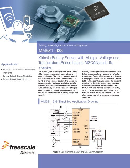
<strong>MM9Z1</strong>_<strong>638</strong> Simplified Application Drawing<br />
An integrated temperature sensor combined <strong>with</strong><br />
battery mounting allows measurement of battery<br />
temperature. Control of the analog die is through<br />
the high performance internal Die-to-Die interface<br />
(D2D), which seamlessly integrates the analog IC<br />
registers into the MCU register map, to provide<br />
faster access than SPI-based systems. The<br />
<strong>MM9Z1</strong>_<strong>638</strong> also includes an internal oscillator,<br />
96 KB or 128 KB of Flash memory, <strong>and</strong> 8.0 KB of<br />
RAM, as well as an ms<strong>CAN</strong> module. Optionally<br />
also multiple external temperature sensors are<br />
supported.<br />
Multiple Cell Monitoring, <strong>CAN</strong> <strong>and</strong> <strong>LIN</strong> Communication
TEST_A<br />
RESET_A<br />
BKGD/MODC<br />
ISENSEH<br />
Current Sense Module<br />
(PGA <strong>with</strong> configurable<br />
Automatic Gain Control)<br />
Internal Bus<br />
Test<br />
Interface<br />
ISENSEL<br />
EXTAL<br />
Reset<br />
Control Module<br />
XTAL<br />
VSENSE3<br />
1/<br />
52<br />
16 Bit<br />
- ADC<br />
<strong>MM9Z1</strong>_<strong>638</strong> Block Diagram<br />
VSENSE2<br />
1/<br />
28<br />
Low Pass Filter<br />
And<br />
Control<br />
VSENSE1<br />
1/<br />
16<br />
TEST<br />
Trimming /<br />
Calibration<br />
Background Debug Controller<br />
VSENSE0<br />
1/<br />
10<br />
16 Bit<br />
- ADC<br />
Internal Bus<br />
PB Low Power Pierce<br />
[1:0]<br />
Oscillator<br />
PLL <strong>with</strong> Freq. Modulation option<br />
OSC Clock Monitor<br />
COP Watchdog<br />
RESET<br />
Periodic Interrupt<br />
Reset Generation <strong>and</strong><br />
Test Entry<br />
Interrupt<br />
Control Module<br />
PA7<br />
Interrupt Module<br />
PTB5<br />
S12Z CPU<br />
Voltage Sense<br />
Module<br />
Debug Module:<br />
4 comparators<br />
64 byte Trace Buffer<br />
PA6<br />
PTB4<br />
4<br />
32-bit ALU<br />
CPU<br />
Register<br />
D2DCLK<br />
PC0<br />
PA5<br />
D2DDAT7<br />
PTB3<br />
EEPROM 4k Bytes <strong>with</strong> ECC<br />
Internal<br />
Temperaure<br />
<strong>Sensor</strong><br />
16 Bit<br />
- ADC<br />
PD7<br />
Control<br />
D2DDAT3<br />
GPIO<br />
4<br />
RAM 8k Bytes <strong>with</strong> ECC<br />
PD3<br />
PA4<br />
D2DDAT6<br />
PTB2<br />
PD6<br />
Flash 128 kByte <strong>with</strong> ECC<br />
D2DDAT2<br />
PD2<br />
PTB1<br />
Die To Die<br />
Interface<br />
PA3<br />
D2DI<br />
D2DDAT5<br />
Temperature Sense<br />
Module<br />
PD5<br />
4<br />
D2DDAT1<br />
ms<strong>CAN</strong><br />
4<br />
PD1<br />
TX<strong>CAN</strong><br />
RX<strong>CAN</strong><br />
PA2<br />
PTB0<br />
D2DDAT4<br />
PTA<br />
DDRA<br />
PD4<br />
D2DDAT0<br />
SS<br />
SCK<br />
PD0<br />
PA1<br />
Wake Up Control Module<br />
(<strong>with</strong> Current Threshold <strong>and</strong><br />
Ampere-Hour Threshold)<br />
SPI<br />
D2DINT<br />
VREG<br />
1.8V Core<br />
2.7V Flash<br />
PC1<br />
MOSI<br />
MISO<br />
PA0<br />
MCU Die<br />
4 Channel Timer<br />
Digital<br />
GPIO<br />
Cascaded<br />
Voltage Regulators<br />
VDDH = 2.5V<br />
(D2D Buffer)<br />
VDDL = 2.5V<br />
(Internal Digital)<br />
VDDA = 2.5V<br />
(Acquisition Chains)<br />
VDDX = 5V<br />
(MCU Core)<br />
SCI<br />
<strong>LIN</strong><br />
Physical<br />
Layer<br />
BIAS<br />
Analog Die<br />
GNDSUB<br />
GNDSUB<br />
GNDSUB<br />
ADCGND<br />
AGND<br />
LGND<br />
<strong>LIN</strong><br />
VSUP<br />
DGND<br />
DGND<br />
VDDL<br />
VDDA<br />
VDDX<br />
VDDH<br />
VDDD2D<br />
VSS1<br />
VDDRX<br />
VSSRX
Features<br />
<strong>Battery</strong> Voltage Measurement<br />
• Dedicated 16-bit second order ΣΔ ADC, full measurement range 3.5 to 28 V, <strong>with</strong> a maximum gain error accuracy of 0.15 percent for 5.0 to<br />
18 V range<br />
• Simultaneous sampling <strong>with</strong> current channel<br />
• Programmable signal filtering shared <strong>with</strong> current measurement<br />
• Four battery voltage measurement w/ internal divider<br />
• Five voltage sensor inputs routable to both voltage <strong>and</strong> temperature channel<br />
Differential battery current measurement<br />
• Dedicated 16-bit second order ΣΔ ADC, <strong>with</strong> a programmable gain amplifier <strong>with</strong> eight programmable gain factors<br />
• Gain control block for automatic gain adjustment<br />
• Measurement range up to +/-2000 A <strong>with</strong> an accuracy of 5.0 mA <strong>and</strong> a resolution of 1.0 mA<br />
Temperature Measurement<br />
• Internal, on-chip temperature sensor<br />
• Dedicated 16-bit ADC <strong>with</strong> anti-aliasing filter<br />
• Accuracy: +/-2.0 °C (-20 to 60 °C) <strong>and</strong> +/-3 °C (-40 to 125 °C)<br />
• Five single ended sensor inputs routable to both voltage <strong>and</strong> temperature channels<br />
• Internal supply for external sensors<br />
Normal <strong>and</strong> Low Power Mode<br />
• Current integration via 32-bit accumulator during low-power mode<br />
• Programmable current threshold detection during low-power mode<br />
• Programmable wake-up timer, triggered wake-up from <strong>LIN</strong><br />
Advanced system level management<br />
• Internal oscillator <strong>with</strong> one percent accuracy<br />
• Communication via <strong>LIN</strong> 2.1, <strong>LIN</strong> 2.0 interface <strong>with</strong> fast mode for Flash programming over <strong>LIN</strong><br />
• An ms<strong>CAN</strong> protocol controller, <strong>with</strong> TxD <strong>and</strong> RxD pins, <strong>and</strong> bus wake-up detection<br />
• S12Z micro controller <strong>with</strong> 128 kByte Flash, 8.0 kByte RAM, 4.0 kByte EE PROM all <strong>with</strong> ECC<br />
• Enhanced VDDX capability to supply MCU <strong>and</strong> external components<br />
• Fast, die-to-die bus interface <strong>with</strong> transparent integration of analog IC registers into the MCU register map, automatic synchronization, <strong>and</strong><br />
error detection<br />
• Automotive EMC <strong>and</strong> ESD performance<br />
Operating conditions<br />
• Ambient operating temperature: -40 °C < T A < 125 °C<br />
• Junction operating temperature: -40 °C < T J < 150 °C
Performance Typical Values<br />
Operating Voltage 3.5 V to 28 V<br />
Ambient Operating Temperature (T A ) -40 °C < T A < 125 °C<br />
Junction Temperature (T J ) -40 °C < T J < 150 °C<br />
Protection Detect Shut Down<br />
<strong>LIN</strong> Bus Line Protection<br />
(Over-temperature)<br />
Customer Benefits<br />
Integration of MCU <strong>and</strong> analog features into a system-in-package solution, results in an optimized, economical, <strong>and</strong> autonomous multifunction<br />
solution, which provides enhanced reliability, <strong>and</strong> requires few external components when compared to discrete solutions<br />
• Fully integrated <strong>and</strong> optimized signal chains, using 3 individual sigma delta ADC to measure current, voltage, <strong>and</strong> temperature<br />
• Optionally five external temperature sense inputs <strong>and</strong> four dedicated <strong>and</strong> five shared voltage sense input<br />
• Four dedicated voltage sense inputs <strong>and</strong> five shared inputs usable either as voltage sense inputs or as external temperature sense inputs<br />
• Reverse battery protected voltage sense pins<br />
• Full <strong>LIN</strong> solution <strong>with</strong> integrated physical interface <strong>and</strong> MS<strong>CAN</strong> module<br />
• Fully AEC-Q100 automotive qualified, <strong>and</strong> designed to meet highest automotive robustness st<strong>and</strong>ards for ESD, EMC, <strong>and</strong> Zero Defect<br />
Quality levels<br />
Questions<br />
• Do you need to monitor battery conditions over a wide current range <strong>with</strong> high precision <strong>and</strong> signal filtering capabilities?<br />
• Do you need a single package solution, integrating a microcontroller, a <strong>LIN</strong> node,ms<strong>CAN</strong>, voltage regulators <strong>and</strong> full battery monitoring<br />
features?<br />
• Do you need high precision synchronous voltage <strong>and</strong> current measurement?<br />
• Are you using a <strong>LIN</strong> or <strong>CAN</strong> communication system?<br />
• Do you need a low current consumption device?<br />
• Do you need a device which is compliant <strong>with</strong> EMC <strong>and</strong> ESD industry st<strong>and</strong>ards?<br />
• Do you need a fully automotive qualified product?<br />
• Do you have to minimize the size of your PCB application?<br />
• Do you need to reduce system cost?<br />
Status<br />
Reporting<br />
• • •
Orderable Part Numbers<br />
Part Number<br />
<strong>MM9Z1</strong>J<strong>638</strong>AM2EP/R2<br />
Flash (kB)<br />
128<br />
RAM (kB)<br />
8.0<br />
EEPROM (kB)<br />
4.0<br />
Temperature<br />
Range T<br />
A<br />
-40 to 125 °C<br />
Package<br />
48 QFN-EP<br />
Documentation<br />
Document Description<br />
<strong>MM9Z1</strong>_<strong>638</strong> Data <strong>Sheet</strong> - Presents the specifications for the product<br />
SG1002 Selector Guide - Analog <strong>and</strong> power management device comparison<br />
SG187 Selector Guide - Automotive device comparison<br />
Development Tools<br />
Part Number Description<br />
KIT9Z1J<strong>638</strong>EVM Evaluation board to demonstrate the key features of the <strong>MM9Z1</strong>_<strong>638</strong>. In development. Contact Sales<br />
(PB-FREE)<br />
48-PIN QFN-EP<br />
98ASA00343D<br />
Freescale: A Leader in Automotive Solutions<br />
Exp<strong>and</strong>ing on its more than 30-year heritage of automotive innovation <strong>and</strong> it’s<br />
high-performance products using <strong>Xtrinsic</strong> technology, Freescale’s SMARTMOS<br />
solutions are designed <strong>with</strong> the right combination of high-performance capability,<br />
processing capacity <strong>and</strong> customizable software to help deliver smart, differentiated<br />
automotive solutions. With <strong>Xtrinsic</strong> Analog, Mixed Signal, <strong>and</strong> Power parts,<br />
our vision is to offer a diverse <strong>and</strong> differentiated product portfolio to meet the<br />
exp<strong>and</strong>ing needs of the automotive, consumer <strong>and</strong> industrial segments. <strong>Xtrinsic</strong><br />
solutions offer ideal blends of functionality <strong>and</strong> intelligence designed to help our<br />
customers differentiate <strong>and</strong> win in highly competitive markets.<br />
For more information, visit freescale.com/<strong>Xtrinsic</strong><br />
Freescale <strong>and</strong> the Freescale logo are trademarks of Freescale Semiconductor, Inc., Reg. U.S. Pat.<br />
& Tm. Off. <strong>Xtrinsic</strong> is the trademark of Freescale Semiconductor, Inc. All other product or service<br />
names are the property of their respective owners. © 2012 Freescale Semiconductor, Inc.<br />
Document Number: <strong>MM9Z1</strong>_<strong>638</strong>FS REV 1.0


