

Mask Set Errata for Mask 3M17W - Freescale Semiconductor
Mask Set Errata for Mask 3M17W - Freescale Semiconductor
Mask Set Errata for Mask 3M17W - Freescale Semiconductor

Create successful ePaper yourself
Turn your PDF publications into a flip-book with our unique Google optimized e-Paper software.
<strong>Freescale</strong> <strong>Semiconductor</strong><br />
<strong>Mask</strong> <strong>Set</strong> <strong>Errata</strong><br />
<strong>Mask</strong> <strong>Set</strong> <strong>Errata</strong> <strong>for</strong> <strong>Mask</strong> <strong>3M17W</strong><br />
Introduction<br />
This report applies to mask <strong>3M17W</strong> <strong>for</strong> these products:<br />
• MPC5674F<br />
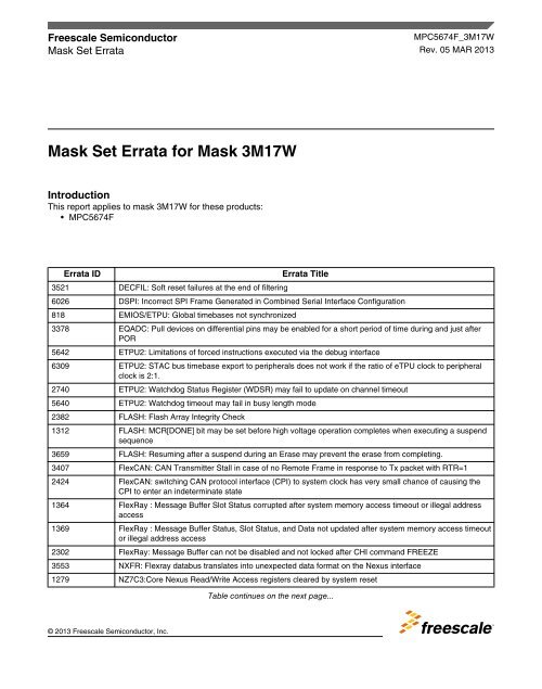
<strong>Errata</strong> ID <strong>Errata</strong> Title<br />
3521 DECFIL: Soft reset failures at the end of filtering<br />
6026 DSPI: Incorrect SPI Frame Generated in Combined Serial Interface Configuration<br />
818 EMIOS/ETPU: Global timebases not synchronized<br />
3378 EQADC: Pull devices on differential pins may be enabled <strong>for</strong> a short period of time during and just after<br />
POR<br />
5642 ETPU2: Limitations of <strong>for</strong>ced instructions executed via the debug interface<br />
6309 ETPU2: STAC bus timebase export to peripherals does not work if the ratio of eTPU clock to peripheral<br />
clock is 2:1.<br />
2740 ETPU2: Watchdog Status Register (WDSR) may fail to update on channel timeout<br />
5640 ETPU2: Watchdog timeout may fail in busy length mode<br />
2382 FLASH: Flash Array Integrity Check<br />
1312 FLASH: MCR[DONE] bit may be set be<strong>for</strong>e high voltage operation completes when executing a suspend<br />
sequence<br />
3659 FLASH: Resuming after a suspend during an Erase may prevent the erase from completing.<br />
3407 FlexCAN: CAN Transmitter Stall in case of no Remote Frame in response to Tx packet with RTR=1<br />
2424 FlexCAN: switching CAN protocol interface (CPI) to system clock has very small chance of causing the<br />
CPI to enter an indeterminate state<br />
1364 FlexRay : Message Buffer Slot Status corrupted after system memory access timeout or illegal address<br />
access<br />
1369 FlexRay : Message Buffer Status, Slot Status, and Data not updated after system memory access timeout<br />
or illegal address access<br />
2302 FlexRay: Message Buffer can not be disabled and not locked after CHI command FREEZE<br />
3553 NXFR: Flexray databus translates into unexpected data <strong>for</strong>mat on the Nexus interface<br />
1279 NZ7C3:Core Nexus Read/Write Access registers cleared by system reset<br />
© 2013 <strong>Freescale</strong> <strong>Semiconductor</strong>, Inc.<br />
Table continues on the next page...<br />
MPC5674F_<strong>3M17W</strong><br />
Rev. 05 MAR 2013
<strong>Errata</strong> ID <strong>Errata</strong> Title<br />
2696 PBRIDGE: Write buffer may cause overflow/underflow of DMA transfers<br />
2996 PIT_RTI: RTI timer corruption when debugging<br />
2322 PMC: LVREH/LVREA/LVRE50 may exit LVI triggered reset with LVI condition still existing<br />
3377 Pad Ring:Nexus pins may drive an unknown value immediately after power up but be<strong>for</strong>e the 1st clock<br />
edge<br />
1419 SIU: Reverting ENGCLK source to the system clock has a very small chance of causing the ENGCLK<br />
generator to enter an indeterminate state<br />
4396 e200z7: Erroneous Address Fetch<br />
3419 e200z: Exceptions generated on speculative prefetch<br />
4480 eQADC: Differential conversions with 4x gain may halt command processing<br />
5086 eQADC: unexpected result may be pushed when Immediate Conversion Command is enabled<br />
2386 eSCI : No LIN frame reception after leaving stop mode<br />
1171 eSCI : DMA stalled after return from stop or doze mode<br />
2396 eSCI : Stop Mode not entered in LIN mode<br />
1297 eSCI : reads of the SCI Data Register, which clears the RDRF flag, may cause loss of frame if read<br />
occurs during reception of the STOP bit<br />
1381 eSCI: LIN Wakeup flag set after aborted LIN frame transmission<br />
1221 eSCI: LIN bit error indicated at start of transmission after LIN reset<br />
e3521: DECFIL: Soft reset failures at the end of filtering<br />
<strong>Errata</strong> type: <strong>Errata</strong><br />
Description: If a software reset of a decimation filter is made exactly at the time it finishes filtering, several<br />
registers reset <strong>for</strong> one clock, but have their values updated by the filtering on the next clock,<br />
including (but not limited to) the integrator current value register DECFIL_CINTVAL and<br />
the tap registers DECFILTER_TAPn.<br />
Workaround: Be<strong>for</strong>e making the soft reset write (DECFIL_MCR bit SRES=1), per<strong>for</strong>m the procedure below:<br />
1- disable filter inputs, writing DECFIL_MCR bit IDIS = 1.<br />
2- read the register DECFIL_MSR and repeat the read until the bit BSY is 0.<br />
3- repeat the loop of step 2; this is necessary to cover the case when a sample is left in the<br />
input buffer.<br />
e6026: DSPI: Incorrect SPI Frame Generated in Combined Serial Interface<br />
Configuration<br />
<strong>Errata</strong> type: <strong>Errata</strong><br />
Description: In the Combined Serial Interface (CSI) configuration of the Deserial Serial Peripheral Interface<br />
(DSPI) where data frames are periodically being sent (Deserial Serial Interface, DSI), a Serial<br />
Peripheral Interface (SPI) frame may be transmitted with incorrect framing.<br />
<strong>Mask</strong> <strong>Set</strong> <strong>Errata</strong> <strong>for</strong> <strong>Mask</strong> <strong>3M17W</strong>, Rev. 05 MAR 2013<br />
2 <strong>Freescale</strong> <strong>Semiconductor</strong>, Inc.
The incorrect frame may occur in this configuration if the user application writes SPI data to the<br />
DSPI Push TX FIFO Register (DSPI_PUSHR) during the last two peripheral clock cycles of the<br />
Delay-after-Transfer (DT) phase. In this case, the SPI frame is corrupted.<br />
Workaround: Workaround 1: Per<strong>for</strong>m SPI FIFO writes after halting the DSPI.<br />
To prevent writing to the FIFO during the last two clock cycles of DT, per<strong>for</strong>m the following<br />
steps every time a SPI frame is required to be transmitted:<br />
Step 1: Halt the DSPI by setting the HALT control bit in the Module Configuration Register<br />
(DSPI_MCR[HALT]).<br />
Step 2: Poll the Status Register's Transmit and Receive Status bit (DSPI_SR[TXRXS]) to<br />
ensure the DSPI has entered the HALT state and completed any in-progress transmission.<br />
Alternatively, if continuous polling is undesirable in the application, wait <strong>for</strong> a fixed time interval<br />
such as 35 baud clocks to ensure completion of any in-progress transmission and then check<br />
once <strong>for</strong> DSPI_SR[TXRXS].<br />
Step 3: Per<strong>for</strong>m the write to DSPI_PUSHR <strong>for</strong> the SPI frame.<br />
Step 4: Clear bit DSPI_MCR[HALT] to bring the DSPI out of the HALT state and return to<br />
normal operation.<br />
Workaround 2: Do not use the CSI configuration. Use the DSPI in either DSI-only mode or<br />
SPI-only mode.<br />
e818: EMIOS/ETPU: Global timebases not synchronized<br />
<strong>Errata</strong> type: <strong>Errata</strong><br />
Description: The eTPU and eMIOS timebases can be started synchronously by asserting the Global Time<br />
Base Enable (GTBE) bit in either the eTPU Module Configuration Register (eTPUMCR) or the<br />
eMIOS Module Configuration Register (eMIOS_MCR). GTBE bits from the eMIOS and eTPU<br />
are ORed together such that asserting either of them allows both eMIOS and eTPU timebases<br />
to start running simultaneously.<br />
When the timebases are running and GTBE is cleared, the timebase and eTPU Angle Counter<br />
(EAC) prescalers can stop at any count. When GTBE is reasserted, the prescalers must have<br />
a determined initialization value so that the timebases will remain in sync with each other.<br />
Workaround: Per<strong>for</strong>m the following steps in sequence to synchronize the time base between the eTPU and<br />
the eMIOS:<br />
1- Clear the Global Time Base Enable (GTBE) bit in the eTPU Module Configuration Register<br />
(ETPUMCR[GTBE] = 0).<br />
2- Clear the Global Time Base Enable (GTBE) and Global Prescaler Enable (GPREN) bits in<br />
the eMIOS Module Configuration Register (EMIOS_MCR[GTBE] = 0, EMIOS_MCR[GPREN] =<br />
0) to stop the Global Clock Prescaler (GCP) from counting.<br />
3- Write the desired counter values to the eTPU Time Counter Registers 1 and 2 (TCR1 and<br />
TCR2) with eTPU microcode (these registers cannot be written by the CPU). This step is<br />
required even if the values in TCR1 and TCR2 are not changed.<br />
4- Clear the Unified Channel Prescaler Enable (UCPREN) bit in the eMIOS Channel Control<br />
Register (EMIOS_CCRn) <strong>for</strong> each of the eMIOS channels (EMIOS_CCRn[UCPREN] = 0).<br />
5- If it is necessary to set the eMIOS counters to known values, configure each eMIOS channel<br />
<strong>for</strong> General Purpose Input (GPI) mode (EMIOS_CCRn[MODE] = 0000000), write the desired<br />
counter values, and restore the desired operational mode (EMIOS_CCRn[MODE] = xxxxxxx).<br />
<strong>Mask</strong> <strong>Set</strong> <strong>Errata</strong> <strong>for</strong> <strong>Mask</strong> <strong>3M17W</strong>, Rev. 05 MAR 2013<br />
<strong>Freescale</strong> <strong>Semiconductor</strong>, Inc. 3
6- <strong>Set</strong> the UCPREN bit in the EMIOS_CCRn register <strong>for</strong> each of the eMIOS channels<br />
(EMIOS_CCRn[UCPREN] = 1) to re-enable the unified channel prescaler.<br />
7- <strong>Set</strong> the GTBE and GPREN bits in the eMIOS MCR simultaneously with a single write<br />
operation(EMIOS_MCR = EMIOS_MCR | 0x14000000).<br />
Note: This works only <strong>for</strong> eTPU and single eMIOS module synchronization. For more than one<br />
eMIOS module there is no workaround, since their GPREN bits cannot be written at the same<br />
time.<br />
e3378: EQADC: Pull devices on differential pins may be enabled <strong>for</strong> a short period of<br />
time during and just after POR<br />
<strong>Errata</strong> type: <strong>Errata</strong><br />
Description: The programmable pull devices (up and down) on the analog differential inputs of the eQADC<br />
may randomly be enabled during the internal Power On Reset (POR) and until the 1st clock<br />
edge propagates through the device. After the first clock edge, the pull resistors will be<br />
disabled until software enables them.<br />
Workaround: Protect any external devices connected to the differential analog inputs. The worst case<br />
condition is with a 1.4K ohm resistor to VDDA (5K pull-up enabled) or VSSA (5K pull-down<br />
enabled). This may also cause temporary additional current requirements on the VDDA supply<br />
of each eQADC module, up to 15 mA on each eQADC if both the pull up and pull down<br />
resistors are enabled simultaneously on all of the differential analog pins.<br />
e5642: ETPU2: Limitations of <strong>for</strong>ced instructions executed via the debug interface<br />
<strong>Errata</strong> type: In<strong>for</strong>mation<br />
Description: The following limitations apply to <strong>for</strong>ced instructions executed through the Nexus debug<br />
interface on the Enhanced Time Processing Unit (ETPU):<br />
1- When a branch or dispatch call instruction with the pipeline flush enabled (field FLS=0) is<br />
<strong>for</strong>ced (through the debug port), the Return Address Register (RAR) is updated with the<br />
current program counter (PC) value, instead of PC value + 1.<br />
2- The Channel Interrupt and Data Transfer Requests (CIRC) instruction field is not<br />
operational.<br />
Workaround: Workaround <strong>for</strong> limitation #1 (branch or dispatch call instruction):<br />
Increment the PC value stored in the RAR by executing a <strong>for</strong>ced Arithmetic Logic Unit (ALU)<br />
instruction after the execution of the branch or dispatch call instruction.<br />
Workaround <strong>for</strong> limitation #2 (CIRC):<br />
To <strong>for</strong>ce an interrupt or DMA request from the debugger:<br />
1- Program a Shared Code Memory (SCM) location with an instruction that issues the interrupt<br />
and/or DMA request. Note: Save the original value at the SCM location.<br />
2- Save the address of the next instruction to be executed.<br />
3- Force a jump with flush to the instruction position.<br />
4- Single-step the execution.<br />
5- Restore the saved value to the SCM location (saved in step 1).<br />
<strong>Mask</strong> <strong>Set</strong> <strong>Errata</strong> <strong>for</strong> <strong>Mask</strong> <strong>3M17W</strong>, Rev. 05 MAR 2013<br />
4 <strong>Freescale</strong> <strong>Semiconductor</strong>, Inc.
6- Force a jump with flush to the address of the next instruction to be executed (saved in step<br />
2).<br />
NOTE: This workaround cannot be executed when the eTPU is in HALT_IDLE state.<br />
e6309: ETPU2: STAC bus timebase export to peripherals does not work if the ratio of<br />
eTPU clock to peripheral clock is 2:1.<br />
<strong>Errata</strong> type: <strong>Errata</strong><br />
Description: The Shared Time Angle Counter (STAC) bus allows an Enhanced Time Processing Unit<br />
(eTPU) to export its timebase or angle counters to another eTPU as well as to other<br />
peripherals such as the Enhanced Modular Input/Output Subsystem (eMIOS) and Enhanced<br />
Queued Analog-to-Digital Converter (eQADC). If the eTPU clock is configured to be twice the<br />
frequency of those peripherals, the STAC bus will not be able to transfer timebase or angle<br />
in<strong>for</strong>mation from the eTPUs to the slower peripherals. The timebase/angle export between<br />
eTPUs, however, is still operational in this configuration.<br />
Workaround: Configure the eTPU clock to the same frequency as peripherals if timebase/angle export to<br />
them is required.<br />
e2740: ETPU2: Watchdog Status Register (WDSR) may fail to update on channel<br />
timeout<br />
<strong>Errata</strong> type: <strong>Errata</strong><br />
Description: The Watchdog Status Register (WDSR) contains a single watchdog status bit <strong>for</strong> each of the<br />
32 eTPU channels per engine. When this bit is set, it indicates that the corresponding channel<br />
encountered a watchdog timeout and was aborted. Under certain conditions the corresponding<br />
bit is not set due to a watchdog timeout, and there<strong>for</strong>e no indication is available as to which<br />
channel timed out. However, the global exception is indicated correctly on a per engine basis,<br />
and the correct exception is issued to the interrupt controller and may be serviced.<br />
Workaround: The application software should treat any watchdog event as a global eTPU exception and<br />
handle it in the eTPU global exception handler. Additionally, during the global exception<br />
handler the application should check the WDSR and clear any bits that may be set by writing<br />
'1' to that bit.<br />
e5640: ETPU2: Watchdog timeout may fail in busy length mode<br />
<strong>Errata</strong> type: <strong>Errata</strong><br />
Description: When the Enhanced Time Processing Unit (eTPU) watchdog is programmed <strong>for</strong> busy length<br />
mode (eTPU Watchdog Timer Register (ETPU_WDTR) Watchdog Mode field (WDM) = 3), a<br />
watchdog timeout will not be detected if all of the conditions below are met:<br />
1- The watchdog timeout occurs at the time slot transition, at the first instruction of a thread, or<br />
at the thread gap. (a thread gap is a 1 microcycle period between threads that service the<br />
same channel).<br />
2- The thread has only one instruction.<br />
3- The eTPU goes idle right after the timed-out thread, or after consecutive single-instruction<br />
threads.<br />
<strong>Mask</strong> <strong>Set</strong> <strong>Errata</strong> <strong>for</strong> <strong>Mask</strong> <strong>3M17W</strong>, Rev. 05 MAR 2013<br />
<strong>Freescale</strong> <strong>Semiconductor</strong>, Inc. 5
Workaround: Insert a NOP instruction in threads which have only one instruction.<br />
e2382: FLASH: Flash Array Integrity Check<br />
<strong>Errata</strong> type: <strong>Errata</strong><br />
Description: The Flash Array Integrity Check (AIC) which may be enabled during the flash user test (UTest)<br />
mode does not return the expected UMn[MISR] values <strong>for</strong> some flash PFCRPn[RWSC] read<br />
wait state configurations. For PFCRPn[RWSC] values of 3-6, the UMn[MISR] signature<br />
computation during AIC does not include the data read from the very last address in the<br />
selected address sequence and thus the UMn[MISR] value is not as expected. For<br />
PFCRPn[RWSC] values of 7, the UMn[MISR] signature computation during AIC will not be<br />
correct as well.<br />
Workaround: The Flash Array Integrity Check is correct <strong>for</strong> PFCRPn[RWSC] values of 0-2. For<br />
PFCRPn[RWSC] values of 3-6, the expected UMn[MISR] values will not include the data read<br />
from the very last address and thus the value expected should be <strong>for</strong> the data read up to the<br />
2nd-last address in the selected address sequence. For a PFCRPn[RWSC] value of 7, the<br />
Array Integrity Check should not be used at all.<br />
e1312: FLASH: MCR[DONE] bit may be set be<strong>for</strong>e high voltage operation completes<br />
when executing a suspend sequence<br />
<strong>Errata</strong> type: <strong>Errata</strong><br />
Description: The program and erase sequence of the flash may be suspended to allow read and program<br />
access to the flash core. An suspend operation is initiated by setting the Erase Suspend<br />
(ESUS) bit or Program Suspend (PSUS) bit in the flash Module Configuration Register (MCR).<br />
<strong>Set</strong>ting a suspend bit causes the flash module to start the sequence which places it in the<br />
suspended state. The user must then wait until the MCR[DONE] bit is set be<strong>for</strong>e a read or<br />
program to the flash is initiated, as the high voltage operation needs to be complete to avoid<br />
errors.<br />
However, during normal read to the same partition, following a suspend sequence, (setting<br />
MCR bit and waiting <strong>for</strong> MCR[DONE] bit to be set) can result in read fails that will return<br />
multiple bit ECC errors. The error is due to the MCR[DONE] bit being set be<strong>for</strong>e the internal<br />
high voltage operation is complete.<br />
Workaround: Because the MCR[DONE] flag can be set too soon, a delay needs to be inserted between<br />
setting the MCR[ESUS] or MCR[PSUS] and reading the same flash partition. The minimum<br />
duration of the delay should be 40us to guarantee correct operation. The <strong>Freescale</strong> flash<br />
programming driver includes this workaround.<br />
e3659: FLASH: Resuming after a suspend during an Erase may prevent the erase from<br />
completing.<br />
<strong>Errata</strong> type: <strong>Errata</strong><br />
Description: If an erase suspend (including the flash put into sleep or disabled mode) is done on any block<br />
in the low Address Space (LAS) or the Mid-Address Space (MAS) except the 16 KB blocks, or<br />
if a suspend is done with multiple non-adjacent blocks (including the High Address Space<br />
[HAS]), the flash state machine may not set the FLASH_MCR[DONE] bit in the flash Module<br />
<strong>Mask</strong> <strong>Set</strong> <strong>Errata</strong> <strong>for</strong> <strong>Mask</strong> <strong>3M17W</strong>, Rev. 05 MAR 2013<br />
6 <strong>Freescale</strong> <strong>Semiconductor</strong>, Inc.
Control Register. This condition only occurs if the suspend occurs during certain internal flash<br />
erase operations. The likelihood of an issue occurring is reduced by limiting the frequency of<br />
suspending the erase operation.<br />
Workaround: If the suspend feature (including disable and sleep modes) of the flash is used, then software<br />
should ensure that if the maximum time allowed <strong>for</strong> an erase operation occurs without a valid<br />
completion flag from the flash (FLASH_MCR[DONE] = 1), the software should abort the erase<br />
operation (by first clearing the Enable High Voltage (FLASH_MCR[EHV] ) bit, then clearing the<br />
Erase read/Write bit (FLASH_MCR[ERS] bit) and the erase operation should be restarted.<br />
Note: The cycle count of the sector is increased by this abort and restart operation.<br />
e3407: FlexCAN: CAN Transmitter Stall in case of no Remote Frame in response to Tx<br />
packet with RTR=1<br />
<strong>Errata</strong> type: <strong>Errata</strong><br />
Description: FlexCAN does not transmit an expected message when the same node detects an incoming<br />
Remote Request message asking <strong>for</strong> any remote answer.<br />
The issue happens when two specific conditions occur:<br />
1) The Message Buffer (MB) configured <strong>for</strong> remote answer (with code "a") is the last MB. The<br />
last MB is specified by Maximum MB field in the Module Configuration Register<br />
(MCR[MAXMB] ).<br />
2) The incoming Remote Request message does not match its ID against the last MB ID.<br />
While an incoming Remote Request message is being received, the FlexCAN also scans the<br />
transmit (Tx) MBs to select the one with the higher priority <strong>for</strong> the next bus arbitration. It is<br />
expected that by the Intermission field it ends up with a selected candidate (winner). The<br />
coincidence of conditions (1) and (2) above creates an internal corner case that cancels the Tx<br />
winner and there<strong>for</strong>e no message will be selected <strong>for</strong> transmission in the next frame. This<br />
gives the appearance that the FlexCAN transmitter is stalled or "stops transmitting".<br />
The problem can be detectable only if the message traffic ceases and the CAN bus enters into<br />
Idle state after the described sequence of events.<br />
There is NO ISSUE if any of the conditions below holds:<br />
a) The incoming message matches the remote answer MB with code "a".<br />
b) The MB configured as remote answer with code "a" is not the last one.<br />
c) Any MB (despite of being Tx or Rx) is reconfigured (by writing its CS field) just after the<br />
Intermission field.<br />
d) A new incoming message sent by any external node starts just after the Intermission field.<br />
Workaround: Do not configure the last MB as a Remote Answer (with code "a").<br />
e2424: FlexCAN: switching CAN protocol interface (CPI) to system clock has very<br />
small chance of causing the CPI to enter an indeterminate state<br />
<strong>Errata</strong> type: <strong>Errata</strong><br />
Description: The reset value <strong>for</strong> the clock source of the CAN protocol interface (CPI) is the oscillator clock.<br />
If the CPI clock source is switched to the system clock while the FlexCAN is not in freeze<br />
mode, then the CPI has a very small chance of entering an indeterminate state.<br />
<strong>Mask</strong> <strong>Set</strong> <strong>Errata</strong> <strong>for</strong> <strong>Mask</strong> <strong>3M17W</strong>, Rev. 05 MAR 2013<br />
<strong>Freescale</strong> <strong>Semiconductor</strong>, Inc. 7
Workaround: Switch the clock source while the FlexCAN is in a halted state by setting HALT bit in the<br />
FlexCAN Module Configuration Register (CANx_MCR[HALT]=1). If the write to the CAN<br />
Control Register to change the clock source (CANx_CR[CLK_SRC]=1) is done in the same<br />
oscillator clock period as the write to CANx_MCR[HALT], then chance of the CPI entering an<br />
indeterminate state is extremely small. If those writes are done on different oscillator clock<br />
periods, then the corruption is impossible. Even if the writes happen back-to-back, as long as<br />
the system clock to oscillator clock frequency ratio is less than three, then the writes will<br />
happen on different oscillator clock periods.<br />
e1364: FlexRay : Message Buffer Slot Status corrupted after system memory access<br />
timeout or illegal address access<br />
<strong>Errata</strong> type: <strong>Errata</strong><br />
Description: If the system memory read access that retrieves the first message buffer header data from a<br />
FlexRay transmit buffer fails due to a system memory access timeout or illegal address<br />
access, it is possible that the slot status in<strong>for</strong>mation <strong>for</strong> the previous slot is written into the<br />
currently used transmit message buffer. In this case, the slot status in<strong>for</strong>mation is not written<br />
into the message buffer assigned to the last slot.<br />
Thus, both the message buffer assigned to the last slot, and the currently used transmit<br />
message buffer contain incorrect slot status in<strong>for</strong>mation.<br />
However, if this occurs, either the System Bus Communication Failure Error Flag (SBCF_EF)<br />
or the Illegal System Bus Address Error Flag (ILSA_EF) will be set in the Controller Host<br />
Interface Error Flag Register (CHIERFR).<br />
Workaround: The FlexRay module and the system memory subsystem should be configured to avoid the<br />
occurrence of system memory access timeouts and illegal address accesses.<br />
In case that one of the error flags CHIERFR[SBCF_EF] or CHIERFR[ILSA_EF] is set, the<br />
application should not use the slot status in<strong>for</strong>mation of the message buffers.<br />
e1369: FlexRay : Message Buffer Status, Slot Status, and Data not updated after<br />
system memory access timeout or illegal address access<br />
<strong>Errata</strong> type: <strong>Errata</strong><br />
Description: If a message buffer is assigned to the last slot in a FlexyRay communication cycle and a<br />
system memory access timeout or illegal address access occurs during the system memory<br />
access in this slot, it is possible that <strong>for</strong> all future communication 1) no slot status in<strong>for</strong>mation<br />
will be written, 2) the message buffer status will not be updated, and 3) no message frames will<br />
be received. If this happens, several message buffers can never be locked by the application.<br />
However, if this occurs, either the System Bus Communication Failure Error Flag (SBCF_EF)<br />
or the Illegal System Bus Address Error Flag (ILSA_EF) will be set in the Controller Host<br />
Interface Error Flag Register (CHIERFR).<br />
Workaround: The FlexRay module and the system memory subsystem should be configured to avoid the<br />
occurrence of system memory access timeouts and illegal address accesses.<br />
In case that one of the error flags CHIERFR[SBCF_EF] or CHIERFR[ILSA_EF] is set, the<br />
application should stop the FlexRay controller via a FREEZE or HALT command and<br />
subsequently restart the controller.<br />
<strong>Mask</strong> <strong>Set</strong> <strong>Errata</strong> <strong>for</strong> <strong>Mask</strong> <strong>3M17W</strong>, Rev. 05 MAR 2013<br />
8 <strong>Freescale</strong> <strong>Semiconductor</strong>, Inc.
e2302: FlexRay: Message Buffer can not be disabled and not locked after CHI<br />
command FREEZE<br />
<strong>Errata</strong> type: <strong>Errata</strong><br />
Description: If a complete message was transmitted from a transmit message buffer or received into a<br />
message buffer and the controller host interface (CHI) command FREEZE is issued by the<br />
application be<strong>for</strong>e the end of the current slot, then this message buffer can not be disabled and<br />
locked until the module has entered the protocol state normal active.<br />
Consequently, this message buffer can not be disabled and locked by the application in the<br />
protocol config state, which prevents the application from clearing the commit bit CMT and the<br />
module from clearing the status bits. The configuration bits in the Message Buffer<br />
Configuration, Control, Status Registers (MBCCSRn) and the message buffer configuration<br />
registers MBCCFRn, MBFIDRn, and MBIDXRn are not affected.<br />
At most one message buffer per channel is affected.<br />
Workaround: There are two types of workaround.<br />
1) The application should not send the CHI command FREEZE and use the CHI command<br />
HALT instead.<br />
2) Be<strong>for</strong>e sending the CHI command FREEZE the application should repeatedly try to disable<br />
all message buffers until all message buffers are disabled. This maximum duration of this task<br />
is three static or three dynamic slots.<br />
e3553: NXFR: Flexray databus translates into unexpected data <strong>for</strong>mat on the Nexus<br />
interface<br />
<strong>Errata</strong> type: <strong>Errata</strong><br />
Description: The data <strong>for</strong>mat <strong>for</strong> Nexus Flexray messages is in little-endian (least significant byte first)<br />
order. This is not currently documented and may be unexpected <strong>for</strong> users of Power<br />
Architecture devices.<br />
For example, in the case of a Flexray System Memory write within the address space<br />
determined by Data Trace Start and Data Trace End Addresses (DTSAx/DTEAx) with the data:<br />
0x1122, the Flexray Nexus interface generates Data Trace Messages (DTM) containing the<br />
data: 0x2211.<br />
Workaround: The user must be aware of the data <strong>for</strong>mat. This will be documented in a future release of the<br />
device reference manual.<br />
e1279: NZ7C3:Core Nexus Read/Write Access registers cleared by system reset<br />
<strong>Errata</strong> type: <strong>Errata</strong><br />
Description: The e200z7 Nexus Read/Write Access registers are cleared when system reset is asserted.<br />
This affects the Read/Write Access Data register (RWD), the Read/Write Access Address<br />
register (RWA), and the Read/write Access Control/Status register (RWCS).<br />
Workaround: Do not expect RWD, RWCS, and RWA to retain values after reset. After reset reload any<br />
values required <strong>for</strong> a transfer.<br />
<strong>Mask</strong> <strong>Set</strong> <strong>Errata</strong> <strong>for</strong> <strong>Mask</strong> <strong>3M17W</strong>, Rev. 05 MAR 2013<br />
<strong>Freescale</strong> <strong>Semiconductor</strong>, Inc. 9
e2696: PBRIDGE: Write buffer may cause overflow/underflow of DMA transfers<br />
<strong>Errata</strong> type: <strong>Errata</strong><br />
Description: Peripheral-paced DMA transfers are controlled by a hardware handshake protocol: when the<br />
peripheral requires a data transfer, it asserts a request to the DMA. The DMA recognizes the<br />
request, activates the corresponding channel and per<strong>for</strong>ms the data transfer, reading from the<br />
source and writing to the destination. As the write is being processed, the DMA sends an<br />
acknowledge back to the peripheral so it can negate its request.<br />
If buffered writes are enabled in the PBRIDGE, there are certain conditions where the DMA's<br />
acknowledge is asserted be<strong>for</strong>e the actual write operation to the peripheral has occurred. The<br />
net effect is the DMA request is not negated properly, causing the DMA to reactivate the<br />
channel, overwriting the last transferred data value be<strong>for</strong>e it is transferred to the peripheral.<br />
Workaround: Do not enable buffered writes <strong>for</strong> the eDMA in the Peripheral Bridge Master Privilege Control<br />
registers (PBRIDGE_A_MPCR and PBRIDGE_B_MPCR), by leaving the MBW4 (eDMA A<br />
master) and MBW5 (eDMA B master) bits cleared. This is the default state of these bits, which<br />
disables buffered writes to the peripherals from both eDMA masters.<br />
e2996: PIT_RTI: RTI timer corruption when debugging<br />
<strong>Errata</strong> type: <strong>Errata</strong><br />
Description: In rare cases, due to a synchronization issue, the Real-Time Interrupt (RTI) timer value may<br />
become corrupted when a breakpoint occurs and the freeze bit is set to pause the timers in<br />
debug mode (PIT_RTI_MCR[FRZ]=0b1).<br />
None of the other timers in the PIT_RTI module are affected. During normal operation (without<br />
debugger attached) there is no impact to the application.<br />
Workaround: When debugging code utilizing the RTI, do not depend on the value of the RTI timer being<br />
correct.<br />
e2322: PMC: LVREH/LVREA/LVRE50 may exit LVI triggered reset with LVI condition<br />
still existing<br />
<strong>Errata</strong> type: In<strong>for</strong>mation<br />
Description: After asserting the Low Voltage Reset Enables PMC_CFGR[LVREH], PMC_CFGR[LVREA],<br />
PMC_CFGR[LVRE50] bits in the PMC, if the voltage ramps down below the LVI voltage on<br />
VDDEHx, VDDA or VDDREG respectively, the part will go to a short power on reset (POR).<br />
After the reset counter has expired, the device will go into normal operation, even though one<br />
or more of the affected supplies may still be below the specified LVI voltage.<br />
Workaround: The part will recover into normal operation, however software should check the status of the<br />
LVIs <strong>for</strong> those segments that are required <strong>for</strong> further operation.<br />
e3377: Pad Ring:Nexus pins may drive an unknown value immediately after power up<br />
but be<strong>for</strong>e the 1st clock edge<br />
<strong>Errata</strong> type: <strong>Errata</strong><br />
<strong>Mask</strong> <strong>Set</strong> <strong>Errata</strong> <strong>for</strong> <strong>Mask</strong> <strong>3M17W</strong>, Rev. 05 MAR 2013<br />
10 <strong>Freescale</strong> <strong>Semiconductor</strong>, Inc.
Description: The Nexus Output pins (Message Data outputs 0:15 [MDO] and Message Start/End outputs<br />
0:1 [MSEO]) may drive an unknown value (high or low) immediately after power up but be<strong>for</strong>e<br />
the 1st clock edge propagates through the device (instead of being weakly pulled low). This<br />
may cause high currents if the pins are tied directly to a supply/ground or any low resistance<br />
driver (when used as a general purpose input [GPI] in the application).<br />
Workaround: 1. Do not tie the Nexus output pins directly to ground or a power supply.<br />
2. If these pins are used as GPI, limit the current to the ability of the regulator supply to<br />
guarantee correct start up of the power supply. Each pin may draw upwards of 150mA.<br />
If not used, the pins may be left unconnected.<br />
e1419: SIU: Reverting ENGCLK source to the system clock has a very small chance of<br />
causing the ENGCLK generator to enter an indeterminate state<br />
<strong>Errata</strong> type: <strong>Errata</strong><br />
Description: The reset value <strong>for</strong> the Engineering Clock (ENGCLK) source is the system clock. If the clock<br />
source is switched to the external clock (buffered crystal frequency or external clock input) by<br />
setting Engineering Clock Source Select bit in the External Clock Control Register<br />
(SIU_ECCR[ECSS]=1) and then reverted to the system clock, then the ENGCLK generator<br />
has a very small chance of entering an indeterminate state.<br />
Workaround: Do not change the ENGCLK source back to the System clock after changing it to the external<br />
clock.<br />
e4396: e200z7: Erroneous Address Fetch<br />
<strong>Errata</strong> type: <strong>Errata</strong><br />
Description: Under certain conditions, if a static branch prediction and a dynamic return prediction (which<br />
uses the subroutine return address stack) occur simultaneously in the Branch Target Buffer<br />
(BTB), the e200z7 core can issue an errant fetch address to the memory system (instruction<br />
fetched from wrong address).<br />
This can only happen when the static branch prediction is "taken" but the branch actually<br />
resolves to "not taken". If the branch resolves to taken, correct fetching occurs <strong>for</strong> this branch<br />
path and no issue is seen.<br />
If Branch Unit Control and Status Register (BUCSR) Branch Prediction Control Static (BPRED)<br />
= 0b00, 0b01, or 0b10, then static branch prediction is configured as "taken". The issue can<br />
occur with these settings.<br />
If BUSCR[BPRED] = 0b11, then static branch prediction is configured as "not taken". The<br />
issue does not occur with this setting.<br />
The issue does not appear in applications compiled with VLE.<br />
Workaround: To prevent the issue from occurring, configure static branch prediction to "not taken" by setting<br />
the Branch Unit Control and Status Register (BUCSR) Branch Prediction Control Static<br />
(BPRED) to 0b11.<br />
For customers using VLE, there is no workaround required, the issue will not be seen.<br />
<strong>Mask</strong> <strong>Set</strong> <strong>Errata</strong> <strong>for</strong> <strong>Mask</strong> <strong>3M17W</strong>, Rev. 05 MAR 2013<br />
<strong>Freescale</strong> <strong>Semiconductor</strong>, Inc. 11
e3419: e200z: Exceptions generated on speculative prefetch<br />
<strong>Errata</strong> type: <strong>Errata</strong><br />
Description: The e200z7 core can prefetch up to 2 cache lines (64 bytes total) beyond the current<br />
instruction execution point. If a bus error occurs when reading any of these prefetch locations,<br />
the machine check exception will be taken. For example, executing code within the last 64<br />
bytes of a memory region such as internal SRAM, may cause a bus error when the core prefetches<br />
past the end of memory. An ECC exception can occur if the core prefetches locations<br />
that are valid, but not yet initialized <strong>for</strong> ECC.<br />
The Boot Assist Monitor (BAM) is located at the end of the address space and so may cause<br />
instruction pre-fetches to wrap-around to address 0 in internal flash memory. If this first block<br />
of flash memory contains ECC errors, such as from an aborted program or erase operation, a<br />
machine-check exception will be asserted. At this point in the boot procedure, exceptions are<br />
disabled, but the machine-check will remain pending and the exception vector will be taken if<br />
user application code subsequently enables the machine check interrupt.<br />
Workaround: Do not place code to be executed within the last 64 bytes of a memory region. When executing<br />
code from internal ECC SRAM, initialize memory beyond the end of the code until the next 32byte<br />
aligned address and then an additional 64 bytes to ensure that prefetches cannot land in<br />
uninitialized SRAM.<br />
To guard against the possibility of the BAM causing a machine-check exception to be taken, as<br />
noted in the errata description, user application code should check and clear the Machine<br />
Check Syndrome Register (MCSR) in the core be<strong>for</strong>e enabling the machine check interrupt.<br />
This can be done by writing all 1s to MCSR.<br />
e4480: eQADC: Differential conversions with 4x gain may halt command processing<br />
<strong>Errata</strong> type: <strong>Errata</strong><br />
Description: If the four times amplifier is enabled <strong>for</strong> a differential analog-to-digital conversion in the<br />
Enhanced Queued Analog to Digital Converter (eQADC) and the ADC clock prescaler is set to<br />
divide by 12 or greater, then the ADC will stop processing commands if a conversion<br />
command is executed immediately after a differential, gain 4x conversion.<br />
Workaround: 1) Do not use a prescaler divide factor greater than or equal to 12 (11 can be used on devices<br />
that support odd prescalers).<br />
2) Insert a dummy write command to any internal ADC register after every 4x conversion<br />
command.<br />
Note 1: If the command FIFO preemption feature is used and it is possible to preempt a FIFO<br />
which contains the 4x conversion + dummy write workaround, then the preempting command<br />
FIFO must be loaded FIRST with a dummy write command and then the desired preempting<br />
conversion command in order to avoid the possibility of following a 4x conversion command<br />
with another conversion command in the same ADC.<br />
Note 2: The level sensitive triggers (when in Low/High Level Gated External Trigger, Single/<br />
Continuous Scan modes) can interrupt the command sequence at any point in time, potentially<br />
breaking the safe sequence 4x conversion command -> dummy write command.<br />
Note 3: When using an odd prescaler (ADCx_CLK_ODD = 1), the duty cycle setting<br />
(ADCxCLK_DTY) must be kept at the default setting of 0.<br />
<strong>Mask</strong> <strong>Set</strong> <strong>Errata</strong> <strong>for</strong> <strong>Mask</strong> <strong>3M17W</strong>, Rev. 05 MAR 2013<br />
12 <strong>Freescale</strong> <strong>Semiconductor</strong>, Inc.
e5086: eQADC: unexpected result may be pushed when Immediate Conversion<br />
Command is enabled<br />
<strong>Errata</strong> type: <strong>Errata</strong><br />
Description: In the enhanced Queued Analog to Digital Converter (eQADC), when the Immediate<br />
Conversion Command is enabled (ICEAn=1) in the eQADC_MCR (Module Configuration<br />
Register), if a conversion from Command First-In-First Out (CFIFO0, conv0) is requested<br />
concurrently with the end-of-conversion from another, lower priority conversion (convx), the<br />
result of the convx is pushed into RFIFOy instead of being simply ignored. Since the convx is<br />
executed again as soon as the critical timing commands have been finished, the command<br />
that triggers convx produces two results instead of one.<br />
Workaround: Workaround 1: Do not use the abort feature (ICEAn=0).<br />
Workaround 2: Arrange the timing of the CFIFO0 trigger such that it does not assert the trigger<br />
at the end of another, lower priority conversion.<br />
Workaround 3: Detect the extra conversion result by checking the EQADC_CFTCRx (EQADC<br />
CFIFO Transfer Counter Register x). This register records how many commands were issued,<br />
so it can be used to check that the expected number of results have been received.<br />
e2386: eSCI : No LIN frame reception after leaving stop mode<br />
<strong>Errata</strong> type: <strong>Errata</strong><br />
Description: When the eSCI module is in LIN mode and transmits or receives an LIN frame, if the CPU<br />
requests Stop Mode, and the Stop Mode is left, an subsequent triggered LIN RX Frame<br />
reception may hang. The module will never assert the eSCI_IFSR2[RXRDY] and<br />
eSCI_IFSR2[TXRDY] flags.<br />
Workaround: The application should ensure that no LIN transmission is running be<strong>for</strong>e it requests Stop<br />
Mode by checking the status of the eSCI_IFSR1[TACT] and eSCI_IFSR1[RACT] status flags.<br />
e1171: eSCI : DMA stalled after return from stop or doze mode<br />
<strong>Errata</strong> type: <strong>Errata</strong><br />
Description: If the eSCI module enters stop or doze mode while the transmit DMA is enabled and<br />
messages are being transmitted, when the CPU exits stop or doze mode, it is possible that<br />
DMA requests will not be generated by the eSCI module.<br />
Workaround: The application should ensure that the eSCI module is idle be<strong>for</strong>e entering the stop mode.<br />
The eSCI module is idle when both transmitter and receiver active status bits in the Interrupt<br />
Flag and Status Register 1 (eSCI_IFSR1) are not set.<br />
The application should not trigger a new transmission on the eSCI module if the application is<br />
preparing <strong>for</strong> the stop mode.<br />
e2396: eSCI : Stop Mode not entered in LIN mode<br />
<strong>Errata</strong> type: <strong>Errata</strong><br />
<strong>Mask</strong> <strong>Set</strong> <strong>Errata</strong> <strong>for</strong> <strong>Mask</strong> <strong>3M17W</strong>, Rev. 05 MAR 2013<br />
<strong>Freescale</strong> <strong>Semiconductor</strong>, Inc. 13
Description: When the eSCI module is in LIN mode and transmits the Header of an LIN RX frame, if the<br />
CPU requests Stop Mode, the eSCI module may not acknowledge the Stop Mode request and<br />
will stay in Normal Operating Mode (not in lower power stop mode).<br />
Workaround: The application should ensure that no LIN transmission is running be<strong>for</strong>e it requests Stop<br />
Mode by checking the Transmit Active and Receive Active status bits in the eSCI Interrupt Flag<br />
and Status Register (eSCI_IFSR1[TACT] and eSCI_IFSR1[RACT]).<br />
e1297: eSCI : reads of the SCI Data Register, which clears the RDRF flag, may cause<br />
loss of frame if read occurs during reception of the STOP bit<br />
<strong>Errata</strong> type: <strong>Errata</strong><br />
Description: A received SCI frame is not written into the SCI Data Registers and the Overrun (OR) flag is<br />
not set in the SCI Status Register 1 (SCISR1), if:<br />
1.) The eSCI has received the last data bit of an SCI frame n<br />
2.) and the Receive Data Register Full (RDRF) flag is still set in the SCISR1 after the reception<br />
of SCI frame n-1<br />
3.) and during the reception of the STOP bit of frame n the host reads the SCI Data Registers,<br />
and clears the RDRF flag<br />
In this case the RDRF flag is erroneously set again by the controller instead of the OR flag.<br />
Thus, the host reads the data of frame n-1 a second time, and the data of frame n is lost.<br />
Workaround: The application should ensure that the data of the <strong>for</strong>egoing frame is read out from the SCI<br />
Data Registers be<strong>for</strong>e the last data bit of the actual frame is received.<br />
e1381: eSCI: LIN Wakeup flag set after aborted LIN frame transmission<br />
<strong>Errata</strong> type: <strong>Errata</strong><br />
Description: If the eSCI module is transmitting a LIN frame and the application sets and clears the LIN<br />
Finite State Machine Resync bit in the LIN Control Register 1 (eSCI_LCR1[LRES]) to abort the<br />
transmission, the LIN Wakeup Receive Flag in the LIN Status Register may be set<br />
(LWAKE=1).<br />
Workaround: If the application has triggered LIN Protocol Engine Reset via the eSCI_LCR1[LRES], it should<br />
wait <strong>for</strong> the duration of a frame and clear the eSCI_IFSR2[LWAKE] flag be<strong>for</strong>e waiting <strong>for</strong> a<br />
wakeup.<br />
e1221: eSCI: LIN bit error indicated at start of transmission after LIN reset<br />
<strong>Errata</strong> type: <strong>Errata</strong><br />
Description: If the eSCI module is in LIN mode and is transmitting a LIN frame, and the application sets and<br />
subsequently clears the LIN reset bit (LRES) in the LIN Control register 1 (ESCI_LCR1), the<br />
next LIN frame transmission might incorrectly signal the occurrence of bit errors<br />
(ESCI_IFSR1[BERR]) and frame error (ESCI_IFSR1[FE]), and the transmitted frame might be<br />
incorrect.<br />
Workaround: There is no generic work around. The implementation of a suitable workaround is highly<br />
dependent on the application and a workaround may not be possible <strong>for</strong> all applications.<br />
<strong>Mask</strong> <strong>Set</strong> <strong>Errata</strong> <strong>for</strong> <strong>Mask</strong> <strong>3M17W</strong>, Rev. 05 MAR 2013<br />
14 <strong>Freescale</strong> <strong>Semiconductor</strong>, Inc.
How to Reach Us:<br />
Home Page:<br />
www.freescale.com<br />
Web Support:<br />
http://www.freescale.com/support<br />
USA/Europe or Locations Not Listed:<br />
<strong>Freescale</strong> <strong>Semiconductor</strong><br />
Technical In<strong>for</strong>mation Center, EL516<br />
2100 East Elliot Road<br />
Tempe, Arizona 85284<br />
+1-800-521-6274 or +1-480-768-2130<br />
www.freescale.com/support<br />
Europe, Middle East, and Africa:<br />
<strong>Freescale</strong> Halbleiter Deutschland GmbH<br />
Technical In<strong>for</strong>mation Center<br />
Schatzbogen 7<br />
81829 Muenchen, Germany<br />
+44 1296 380 456 (English)<br />
+46 8 52200080 (English)<br />
+49 89 92103 559 (German)<br />
+33 1 69 35 48 48 (French)<br />
www.freescale.com/support<br />
Japan:<br />
<strong>Freescale</strong> <strong>Semiconductor</strong> Japan Ltd.<br />
Headquarters<br />
ARCO Tower 15F<br />
1-8-1, Shimo-Meguro, Meguro-ku,<br />
Tokyo 153-0064<br />
Japan<br />
0120 191014 or +81 3 5437 9125<br />
support.japan@freescale.com<br />
Asia/Pacific:<br />
<strong>Freescale</strong> <strong>Semiconductor</strong> China Ltd.<br />
Exchange Building 23F<br />
No. 118 Jianguo Road<br />
Chaoyang District<br />
Beijing 100022<br />
China<br />
+86 10 5879 8000<br />
support.asia@freescale.com<br />
Document Number: MPC5674F_<strong>3M17W</strong><br />
Rev. 05 MAR 2013<br />
In<strong>for</strong>mation in this document is provided solely to enable system and software<br />
implementers to use <strong>Freescale</strong> <strong>Semiconductor</strong>s products. There are no express or implied<br />
copyright licenses granted hereunder to design or fabricate any integrated circuits or<br />
integrated circuits based on the in<strong>for</strong>mation in this document.<br />
<strong>Freescale</strong> <strong>Semiconductor</strong> reserves the right to make changes without further notice to any<br />
products herein. <strong>Freescale</strong> <strong>Semiconductor</strong> makes no warranty, representation, or<br />
guarantee regarding the suitability of its products <strong>for</strong> any particular purpose, nor does<br />
<strong>Freescale</strong> <strong>Semiconductor</strong> assume any liability arising out of the application or use of any<br />
product or circuit, and specifically disclaims any liability, including without limitation<br />
consequential or incidental damages. "Typical" parameters that may be provided in<br />
<strong>Freescale</strong> <strong>Semiconductor</strong> data sheets and/or specifications can and do vary in different<br />
applications and actual per<strong>for</strong>mance may vary over time. All operating parameters,<br />
including "Typicals", must be validated <strong>for</strong> each customer application by customer's<br />
technical experts. <strong>Freescale</strong> <strong>Semiconductor</strong> does not convey any license under its patent<br />
rights nor the rights of others. <strong>Freescale</strong> <strong>Semiconductor</strong> products are not designed,<br />
intended, or authorized <strong>for</strong> use as components in systems intended <strong>for</strong> surgical implant<br />
into the body, or other applications intended to support or sustain life, or <strong>for</strong> any other<br />
application in which failure of the <strong>Freescale</strong> <strong>Semiconductor</strong> product could create a<br />
situation where personal injury or death may occur. Should Buyer purchase or use<br />
<strong>Freescale</strong> <strong>Semiconductor</strong> products <strong>for</strong> any such unintended or unauthorized application,<br />
Buyer shall indemnify <strong>Freescale</strong> <strong>Semiconductor</strong> and its officers, employees, subsidiaries,<br />
affiliates, and distributors harmless against all claims, costs, damages, and expenses, and<br />
reasonable attorney fees arising out of, directly or indirectly, any claim of personal injury<br />
or death associated with such unintended or unauthorized use, even if such claims alleges<br />
that <strong>Freescale</strong> <strong>Semiconductor</strong> was negligent regarding the design or manufacture of<br />
the part.<br />
RoHS-compliant and/or Pb-free versions of <strong>Freescale</strong> products have the functionality and<br />
electrical characteristics as their non-RoHS-complaint and/or non-Pb-free counterparts.<br />
For further in<strong>for</strong>mation, see http://www.freescale.com or contact your <strong>Freescale</strong><br />
sales representative.<br />
For in<strong>for</strong>mation on <strong>Freescale</strong>'s Environmental Products program, go to<br />
http://www.freescale.com/epp.<br />
<strong>Freescale</strong> and the <strong>Freescale</strong> logo are trademarks of <strong>Freescale</strong> <strong>Semiconductor</strong>, Inc.<br />
All other product or service names are the property of their respective owners.<br />
© 2013 <strong>Freescale</strong> <strong>Semiconductor</strong>, Inc.


