

Data Sheet - Freescale Semiconductor
Data Sheet - Freescale Semiconductor
Data Sheet - Freescale Semiconductor

You also want an ePaper? Increase the reach of your titles
YUMPU automatically turns print PDFs into web optimized ePapers that Google loves.
General<br />
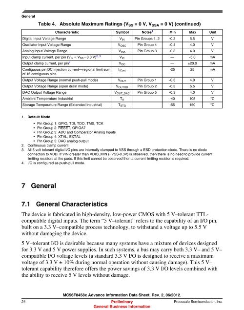
Table 4. Absolute Maximum Ratings (V SS = 0 V, V SSA = 0 V) (continued)<br />
Characteristic Symbol Notes 1 Min Max Unit<br />
Digital Input Voltage Range V IN Pin Groups 1, 2 -0.3 5.5 V<br />
Oscillator Input Voltage Range V OSC Pin Group 4 -0.4 4.0 V<br />
Analog Input Voltage Range V INA Pin Group 3 -0.3 4.0 V<br />
Input clamp current, per pin (V IN < V SS - 0.3 V) 2, 3 V IC — -5.0 mA<br />
Output clamp current, per pin 4 V OC — ±20.0 mA<br />
Contiguous pin DC injection current—regional limit sum<br />
of 16 contiguous pins<br />
I ICont -25 25 mA<br />
Output Voltage Range (normal push-pull mode) V OUT Pin Group 1 -0.3 4.0 V<br />
Output Voltage Range (open drain mode) V OUTOD Pin Group 2 -0.3 5.5 V<br />
DAC Output Voltage Range V OUT_DAC Pin Group 5 -0.3 4.0 V<br />
Ambient Temperature Industrial T A -40 105 °C<br />
Storage Temperature Range (Extended Industrial) T STG -55 150 °C<br />
1. Default Mode<br />
• Pin Group 1: GPIO, TDI, TDO, TMS, TCK<br />
• Pin Group 2: RESET, GPIOA7<br />
• Pin Group 3: ADC and Comparator Analog Inputs<br />
• Pin Group 4: XTAL, EXTAL<br />
• Pin Group 5: DAC analog output<br />
2. Continuous clamp current<br />
3. All 5 volt tolerant digital I/O pins are internally clamped to VSS through a ESD protection diode. There is no diode<br />
connection to VDD. If VIN greater than VDIO_MIN (=VSS-0.3V) is observed, then there is no need to provide current<br />
limiting resistors at the pads. If this limit cannot be observed then a current limiting resistor is required.<br />
4. I/O is configured as push-pull mode.<br />
7 General<br />
7.1 General Characteristics<br />
The device is fabricated in high-density, low-power CMOS with 5 V–tolerant TTLcompatible<br />
digital inputs. The term “5 V–tolerant” refers to the capability of an I/O pin,<br />
built on a 3.3 V–compatible process technology, to withstand a voltage up to 5.5 V<br />
without damaging the device.<br />
5 V–tolerant I/O is desirable because many systems have a mixture of devices designed<br />
for 3.3 V and 5 V power supplies. In such systems, a bus may carry both 3.3 V– and 5 V–<br />
compatible I/O voltage levels (a standard 3.3 V I/O is designed to receive a maximum<br />
voltage of 3.3 V ± 10% during normal operation without causing damage). This 5 V–<br />
tolerant capability therefore offers the power savings of 3.3 V I/O levels combined with<br />
the ability to receive 5 V levels without damage.<br />
MC56F8458x Advance Information <strong>Data</strong> <strong>Sheet</strong>, Rev. 2, 06/2012.<br />
24 Preliminary <strong>Freescale</strong> <strong>Semiconductor</strong>, Inc.<br />
General Business Information


