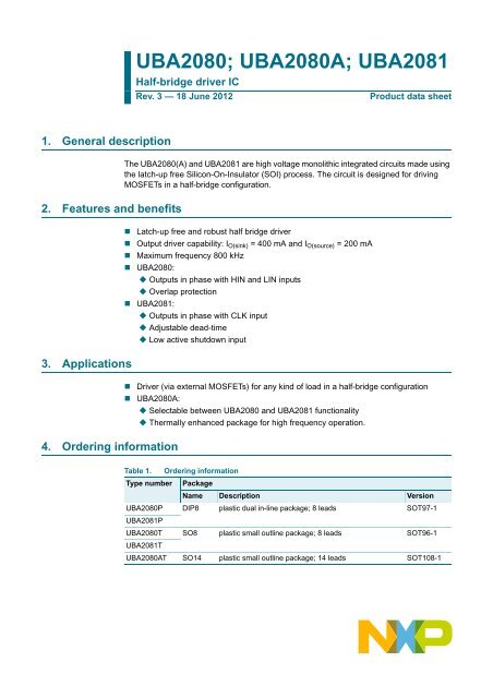
UBA2080_UBA2081 - NXP Semiconductors
UBA2080_UBA2081 - NXP Semiconductors
UBA2080_UBA2081 - NXP Semiconductors

Create successful ePaper yourself
Turn your PDF publications into a flip-book with our unique Google optimized e-Paper software.
1. General description<br />
2. Features and benefits<br />
3. Applications<br />
4. Ordering information<br />
<strong>UBA2080</strong>; <strong>UBA2080</strong>A; <strong>UBA2081</strong><br />
Half-bridge driver IC<br />
Rev. 3 — 18 June 2012 Product data sheet<br />
The <strong>UBA2080</strong>(A) and <strong>UBA2081</strong> are high voltage monolithic integrated circuits made using<br />
the latch-up free Silicon-On-Insulator (SOI) process. The circuit is designed for driving<br />
MOSFETs in a half-bridge configuration.<br />
Latch-up free and robust half bridge driver<br />
Output driver capability: IO(sink) = 400 mA and IO(source) = 200 mA<br />
Maximum frequency 800 kHz<br />
<strong>UBA2080</strong>:<br />
Outputs in phase with HIN and LIN inputs<br />
Overlap protection<br />
<strong>UBA2081</strong>:<br />
Outputs in phase with CLK input<br />
Adjustable dead-time<br />
Low active shutdown input<br />
Driver (via external MOSFETs) for any kind of load in a half-bridge configuration<br />
<strong>UBA2080</strong>A:<br />
Selectable between <strong>UBA2080</strong> and <strong>UBA2081</strong> functionality<br />
Thermally enhanced package for high frequency operation.<br />
Table 1. Ordering information<br />
Type number Package<br />
Name Description Version<br />
<strong>UBA2080</strong>P<br />
<strong>UBA2081</strong>P<br />
DIP8 plastic dual in-line package; 8 leads SOT97-1<br />
<strong>UBA2080</strong>T<br />
<strong>UBA2081</strong>T<br />
SO8 plastic small outline package; 8 leads SOT96-1<br />
<strong>UBA2080</strong>AT SO14 plastic small outline package; 14 leads SOT108-1
<strong>NXP</strong> <strong>Semiconductors</strong> <strong>UBA2080</strong>; <strong>UBA2080</strong>A; <strong>UBA2081</strong><br />
5. Block diagram<br />
VDD<br />
HIN<br />
ULVO ULVO R1<br />
HS DRIVER<br />
R2 S<br />
LOGIC<br />
Fig 1. Block diagram (<strong>UBA2080</strong> and <strong>UBA2080</strong>A with select = GND)<br />
VDD<br />
LIN<br />
OVERLAP<br />
PROTECTION<br />
SEL<br />
LEVEL SHIFTER<br />
LOGIC<br />
CLK LEVEL SHIFTER<br />
SD<br />
Vref<br />
LS DRIVER<br />
aaa-001102<br />
ULVO ULVO R1<br />
HS DRIVER<br />
R2 S<br />
NON-OVERLAP<br />
Fig 2. Block diagram (<strong>UBA2080</strong>A and <strong>UBA2081</strong> with select = VDD)<br />
Half-bridge driver IC<br />
Refer to Figure 7 and Figure 8 for detailed information on the required application<br />
components.<br />
<strong>UBA2080</strong>_<strong>UBA2081</strong> All information provided in this document is subject to legal disclaimers. © <strong>NXP</strong> B.V. 2012. All rights reserved.<br />
Product data sheet Rev. 3 — 18 June 2012 2 of 15<br />
SEL<br />
LS DRIVER<br />
aaa-001107<br />
FS<br />
GH<br />
SH<br />
GL<br />
GND<br />
FS<br />
GH<br />
SH<br />
GL<br />
GND
<strong>NXP</strong> <strong>Semiconductors</strong> <strong>UBA2080</strong>; <strong>UBA2080</strong>A; <strong>UBA2081</strong><br />
6. Pinning information<br />
VDD<br />
1<br />
6.1 Pinning<br />
GL<br />
GND 2<br />
<strong>UBA2080</strong><br />
7 SH<br />
LIN 3<br />
6 GH<br />
HIN 4<br />
5 FS<br />
aaa-001121<br />
Fig 3. <strong>UBA2080</strong>: Pin<br />
configuration DIP8 and<br />
SO8 package<br />
8<br />
6.2 Pin description<br />
GND 1<br />
14 SEL<br />
GND 2<br />
13 GND<br />
SD/LIN 3<br />
12 VDD<br />
GND 4 <strong>UBA2080</strong>A 11 GL<br />
CLK/HIN 5<br />
10 GND<br />
FS 6<br />
9 GND<br />
GH 7 8 SH<br />
aaa-001134<br />
Fig 4. <strong>UBA2080</strong>A: Pin<br />
configuration SO14<br />
package<br />
Half-bridge driver IC<br />
GND 2<br />
<strong>UBA2081</strong><br />
7 SH<br />
SD 3<br />
6 GH<br />
Fig 5. <strong>UBA2081</strong>: Pin<br />
configuration DIP8 and<br />
SO8 package<br />
<strong>UBA2080</strong>_<strong>UBA2081</strong> All information provided in this document is subject to legal disclaimers. © <strong>NXP</strong> B.V. 2012. All rights reserved.<br />
Product data sheet Rev. 3 — 18 June 2012 3 of 15<br />
VDD<br />
1<br />
GL<br />
CLK 4<br />
5 FS<br />
aaa-001126<br />
Table 2. Pin description <strong>UBA2080</strong>/<strong>UBA2081</strong> DIP8 and SO8<br />
Symbol Pin Description<br />
<strong>UBA2080</strong> <strong>UBA2081</strong><br />
(DIP8/SO8) (DIP8/SO8)<br />
VDD 1 IC supply<br />
GND 2 IC ground and low-side driver return<br />
LIN 3 - low-side driver logic input<br />
SD - 3 low active analog shutdown input and non-overlap time<br />
setting<br />
HIN 4 - high-side driver logic input<br />
CLK - 4 clock logic input<br />
FS 5 floating supply voltage<br />
GH 6 high-side MOSFET gate<br />
SH 7 high-side MOSFET source<br />
GL 8 low-side MOSFET gate<br />
Table 3. Pin description <strong>UBA2080</strong>AT (SO14)<br />
Symbol Pin Description<br />
GND 1, 2, 4, 9, 10, 13 IC ground and low side driver return<br />
SD/LIN 3 low-side driver logic input or low active shutdown and<br />
non-overlap time setting<br />
CLK/HIN 5 high-side driver logic input or clock logic input<br />
FS 6 floating supply voltage<br />
SH 8 high-side MOSFET source<br />
8
<strong>NXP</strong> <strong>Semiconductors</strong> <strong>UBA2080</strong>; <strong>UBA2080</strong>A; <strong>UBA2081</strong><br />
7. Functional description<br />
7.1 Start-up state<br />
Half-bridge driver IC<br />
Table 3. Pin description <strong>UBA2080</strong>AT (SO14) …continued<br />
Symbol Pin Description<br />
GH 7 high-side MOSFET gate<br />
GL 11 low-side MOSFET gate<br />
VDD 12 IC supply<br />
SEL 14 select <strong>UBA2080</strong> or <strong>UBA2081</strong> functionality; only connect to<br />
GND or VDD<br />
The IC enters the start-up state when the supply voltage on pin VDD increases. In the<br />
start-up state, the high-side power transistor is non-conducting and the low-side power<br />
transistor is switched on. The internal circuit is reset and the capacitor on the bootstrap pin<br />
FS is charged. The start-up state is defined until the value of VDD =theVDD(start) value.<br />
After which the IC switches to the oscillation state.<br />
The circuit enters the start-up state again when the voltage on pin VDD < VDD(stop).<br />
7.2 <strong>UBA2080</strong> oscillation state<br />
In the oscillation state, the output voltage of the GL and GH drivers depend on the logical<br />
signals HIN and LIN (see Table 4).<br />
To prevent cross conduction in the half-bridge MOSFETs, the combination HIN = LIN = 1<br />
is not allowed. Both GL and GH are LOW under this condition.<br />
Table 4. <strong>UBA2080</strong> Logic table<br />
State HIN LIN GH GL<br />
Start-up - - LOW HIGH<br />
Oscillation 0 0 LOW LOW<br />
Oscillation 0 1 LOW HIGH<br />
Oscillation 1 0 HIGH LOW<br />
Oscillation 1 1 LOW LOW<br />
7.3 <strong>UBA2081</strong> oscillation state<br />
In the oscillation state, the output voltage of the GL and GH drivers depend on the logical<br />
signals CLK and SD (see Table 5).<br />
Table 5. <strong>UBA2081</strong> Logic table<br />
State CLK SD GH GL<br />
Start-up - - LOW HIGH<br />
Oscillation 0 0 LOW HIGH<br />
Oscillation 1 0 HIGH LOW<br />
Oscillation 0 1 LOW LOW<br />
Oscillation 1 1 LOW LOW<br />
<strong>UBA2080</strong>_<strong>UBA2081</strong> All information provided in this document is subject to legal disclaimers. © <strong>NXP</strong> B.V. 2012. All rights reserved.<br />
Product data sheet Rev. 3 — 18 June 2012 4 of 15
<strong>NXP</strong> <strong>Semiconductors</strong> <strong>UBA2080</strong>; <strong>UBA2080</strong>A; <strong>UBA2081</strong><br />
7.4 <strong>UBA2081</strong> non-overlap time<br />
Half-bridge driver IC<br />
The external resistor (RSD) on pin SD sets the non-overlap time of the <strong>UBA2081</strong>. The<br />
relationship between this resistor value and actual dead-time is listed in Figure 6.<br />
It is essential to add a 10 nF to 100 nF decoupling capacitor across RSD to ensure a noise<br />
immune dead-time system.<br />
3000<br />
tno<br />
(ns)<br />
2000<br />
1000<br />
Fig 6. Non-overlap time versus SD resistor (RSD)<br />
7.5 <strong>UBA2081</strong> shutdown protection<br />
When the voltage at pin SD is pulled below VIH, the internal sink drivers of the pins GL and<br />
GH are immediately enabled to switch off the external power MOSFETs.<br />
The shutdown comparator has a hysteresis of Vhys(SD) to avoid multiple switching.<br />
Preferably, pin SD is pulled low via a collector of a transistor (see application schematic)<br />
to avoid loading of this pin (Influences the non-overlap time settings) at normal operation.<br />
7.6 <strong>UBA2080</strong> overlap protection<br />
The internal logic takes care that the GL driver and GH driver are both set to LOW in this<br />
situation to avoid that HIN = LIN = 1 causes a cross current in the external half-bridge.<br />
7.7 <strong>UBA2080</strong>A select function<br />
aaa-001135<br />
0<br />
0 1 2<br />
RSD (MΩ)<br />
3<br />
Pin SEL enables the selection of either the <strong>UBA2080</strong> or the <strong>UBA2081</strong> functionality.<br />
SEL = 0 gives the <strong>UBA2080</strong> functionality. SEL = VDD gives the <strong>UBA2081</strong> functionality.<br />
<strong>UBA2080</strong>_<strong>UBA2081</strong> All information provided in this document is subject to legal disclaimers. © <strong>NXP</strong> B.V. 2012. All rights reserved.<br />
Product data sheet Rev. 3 — 18 June 2012 5 of 15
<strong>NXP</strong> <strong>Semiconductors</strong> <strong>UBA2080</strong>; <strong>UBA2080</strong>A; <strong>UBA2081</strong><br />
8. Limiting values<br />
Half-bridge driver IC<br />
Table 6. Limiting values<br />
In accordance with the Absolute Maximum Rating System (IEC 60134).<br />
Symbol Parameter Conditions Min Max Unit<br />
VDD supply voltage nominal 0 15.5 V<br />
VFS voltage on pin FS VSH VSH +15.5 V<br />
VSH voltage on pin SH source high-side MOSFET −3 +600 V<br />
t
<strong>NXP</strong> <strong>Semiconductors</strong> <strong>UBA2080</strong>; <strong>UBA2080</strong>A; <strong>UBA2081</strong><br />
10. Characteristics<br />
Half-bridge driver IC<br />
Table 8. Characteristics<br />
Tj = 25 °C; all voltages are measured with respect to SGND; VDD = 12.8 V; positive currents flow into the IC.<br />
Symbol Parameter Conditions Min Typ Max Unit<br />
High-voltage supply<br />
Ileak<br />
Start-up state<br />
leakage current FS = GH = SH = 600 V - - 10 μA<br />
IVDD current on pin VDD 420 520 620 μA<br />
VDD(start) start supply voltage 11 12 13 V<br />
VDD(stop) stop supply voltage 8 8.5 9 V<br />
VDD(hys)<br />
Pin LIN input<br />
hysteresis of supply voltage start-to-stop 3 3.5 4 V<br />
VIH HIGH-level input voltage 1.6 2.2 2.8 V<br />
Vhys(LIN) hysteresis voltage on pin LIN - 400 - mV<br />
II(LIN)<br />
Pin HIN input<br />
input current on pin LIN - 0 1 μA<br />
VIH HIGH-level input voltage 1.6 2.2 2.8 V<br />
Vhys(HIN) hysteresis voltage on pin HIN - 400 - mV<br />
II(HIN)<br />
Pin CLK input<br />
input current on pin HIN - 0 1 μA<br />
VIH HIGH-level input voltage 2.7 - - V<br />
VIL LOW-level input voltage - - 0.8 V<br />
II(CLK)<br />
Pin SD input<br />
input current on pin CLK - 0 1 μA<br />
VIH HIGH-level input voltage to activate shutdown 1.6 2.2 2.8 V<br />
Vhys(SD) hysteresis voltage on pin SD - 400 - mV<br />
tno non-overlap time RSD = 100 kΩ; typical minimum - 140 - ns<br />
Pin SEL input<br />
RSD =3MΩ; typical maximum - 2.4 - μs<br />
II(SEL)<br />
gate drivers<br />
input current on pin SEL - 0 1 μA<br />
IO(source) output source current VFS =VVDD =12V; VSH =0V;<br />
VGH =VGL =8V<br />
- 200 - mA<br />
IO(sink) output sink current VFS =VVDD =12V; VSH =0V;<br />
VGH =VGL =4V<br />
- 400 - mA<br />
Vd(bs) bootstrap diode voltage Id(bs) =20mA - 2.3 - V<br />
VUVLO undervoltage lockout voltage reset 3.6 4.2 4.8 V<br />
IFS<br />
Timing<br />
current on pin FS VFS =VVDD =12V; VSH =0V 27 32 37 μA<br />
tPD propagation delay <strong>UBA2080</strong>; matching;<br />
C(GL) =C(GH) = 0, propagation time<br />
difference between GL and GH.<br />
- 50 - ns<br />
<strong>UBA2080</strong>_<strong>UBA2081</strong> All information provided in this document is subject to legal disclaimers. © <strong>NXP</strong> B.V. 2012. All rights reserved.<br />
Product data sheet Rev. 3 — 18 June 2012 7 of 15
<strong>NXP</strong> <strong>Semiconductors</strong> <strong>UBA2080</strong>; <strong>UBA2080</strong>A; <strong>UBA2081</strong><br />
11. Application information<br />
Half-bridge driver IC<br />
Table 8. Characteristics …continued<br />
Tj = 25 °C; all voltages are measured with respect to SGND; VDD = 12.8 V; positive currents flow into the IC.<br />
Symbol Parameter Conditions Min Typ Max Unit<br />
tPD(LIN-GL) propagation delay from LIN to<br />
GL<br />
<strong>UBA2080</strong>; C(GL) =0pF - 240 - ns<br />
tPD(HIN-GH) propagation delay from HIN to<br />
GH<br />
<strong>UBA2080</strong>; C(GH) = 0 pF - 180 - ns<br />
fmax maximum frequency 800 - - kHz<br />
Fig 7. Typical <strong>UBA2080</strong> application<br />
shutdown<br />
from μC<br />
VDD supply<br />
tno<br />
CVDD<br />
HIN<br />
LIN<br />
VDD<br />
input clock<br />
RSD<br />
VDD supply<br />
Remark: The capacitor connected to the SD pin ensures a noise immune dead-time.<br />
Fig 8. Typical <strong>UBA2081</strong> application<br />
<strong>UBA2080</strong><br />
<strong>UBA2080</strong>_<strong>UBA2081</strong> All information provided in this document is subject to legal disclaimers. © <strong>NXP</strong> B.V. 2012. All rights reserved.<br />
Product data sheet Rev. 3 — 18 June 2012 8 of 15<br />
CVDD<br />
SD<br />
CLK<br />
VDD<br />
GND<br />
FS<br />
GH<br />
SH<br />
GL<br />
<strong>UBA2081</strong><br />
GND<br />
HVIN<br />
FS<br />
GH<br />
SH<br />
GL<br />
CFS<br />
to load<br />
aaa-001424<br />
HVIN<br />
CFS<br />
to load<br />
aaa-001425
<strong>NXP</strong> <strong>Semiconductors</strong> <strong>UBA2080</strong>; <strong>UBA2080</strong>A; <strong>UBA2081</strong><br />
12. Package outline<br />
DIMENSIONS (inch dimensions are derived from the original mm dimensions)<br />
UNIT<br />
mm<br />
inches<br />
A<br />
max.<br />
1.75<br />
0.25<br />
0.10<br />
0.069 0.010<br />
0.004<br />
OUTLINE<br />
VERSION<br />
Fig 9. Package outline SOT96-1 (SO8)<br />
Half-bridge driver IC<br />
SO8: plastic small outline package; 8 leads; body width 3.9 mm SOT96-1<br />
A1 A2 A3 bp c D (1) E (2) (1)<br />
e HE L LpQ v w y Z θ<br />
1.45<br />
1.25<br />
0.25<br />
0.49<br />
0.36<br />
0.25<br />
0.19<br />
5.0<br />
4.8<br />
0.20<br />
0.19<br />
4.0<br />
3.8<br />
0.16<br />
0.15<br />
REFERENCES<br />
1.27<br />
IEC JEDEC JEITA<br />
6.2<br />
5.8<br />
0.244<br />
0.228<br />
Notes<br />
1. Plastic or metal protrusions of 0.15 mm (0.006 inch) maximum per side are not included.<br />
2. Plastic or metal protrusions of 0.25 mm (0.01 inch) maximum per side are not included.<br />
SOT96-1<br />
8<br />
1<br />
0.057<br />
0.049<br />
Z<br />
y<br />
pin 1 index<br />
e<br />
0.01<br />
D<br />
0.019<br />
0.014<br />
0.0100<br />
0.0075<br />
bp<br />
076E03 MS-012<br />
5<br />
4<br />
w M<br />
c<br />
A2<br />
A1<br />
0 2.5 5 mm<br />
scale<br />
0.05<br />
EUROPEAN<br />
PROJECTION<br />
ISSUE DATE<br />
<strong>UBA2080</strong>_<strong>UBA2081</strong> All information provided in this document is subject to legal disclaimers. © <strong>NXP</strong> B.V. 2012. All rights reserved.<br />
Product data sheet Rev. 3 — 18 June 2012 9 of 15<br />
E<br />
HE<br />
detail X<br />
Q<br />
L p<br />
L<br />
A<br />
(A )<br />
3<br />
θ<br />
A<br />
X<br />
v M A<br />
1.0 0.7<br />
0.7<br />
1.05<br />
0.25 0.25 0.1<br />
0.4 0.6<br />
0.3 o<br />
8<br />
o<br />
0.039 0.028<br />
0.028 0<br />
0.041 0.01 0.01 0.004<br />
0.016 0.024<br />
0.012<br />
99-12-27<br />
03-02-18
<strong>NXP</strong> <strong>Semiconductors</strong> <strong>UBA2080</strong>; <strong>UBA2080</strong>A; <strong>UBA2081</strong><br />
OUTLINE<br />
VERSION<br />
SOT97-1<br />
Fig 10. Package outline SOT97-1 (DIP8)<br />
REFERENCES<br />
IEC JEDEC JEITA<br />
EUROPEAN<br />
PROJECTION<br />
Half-bridge driver IC<br />
DIP8: plastic dual in-line package; 8 leads (300 mil) SOT97-1<br />
DIMENSIONS (inch dimensions are derived from the original mm dimensions)<br />
UNIT<br />
A<br />
max.<br />
A 1<br />
min.<br />
A 2<br />
max.<br />
b b1 b2 c<br />
(1)<br />
D<br />
(1)<br />
E e e1 L ME MH w<br />
(1)<br />
Z<br />
max.<br />
mm<br />
inches<br />
seating plane<br />
L<br />
Z<br />
4.2 0.51 3.2<br />
0.17 0.02 0.13<br />
8<br />
1<br />
b<br />
1.73<br />
1.14<br />
0.068<br />
0.045<br />
D<br />
e<br />
pin 1 index<br />
0.53<br />
0.38<br />
0.021<br />
0.015<br />
1.07<br />
0.89<br />
0.042<br />
0.035<br />
0.36<br />
0.23<br />
0.014<br />
0.009<br />
9.8<br />
9.2<br />
0.39<br />
0.36<br />
050G01 MO-001 SC-504-8<br />
b 1<br />
5<br />
4<br />
A 1<br />
b 2<br />
A 2<br />
w M<br />
E<br />
A<br />
0 5 10 mm<br />
scale<br />
ISSUE DATE<br />
99-12-27<br />
03-02-13<br />
<strong>UBA2080</strong>_<strong>UBA2081</strong> All information provided in this document is subject to legal disclaimers. © <strong>NXP</strong> B.V. 2012. All rights reserved.<br />
Product data sheet Rev. 3 — 18 June 2012 10 of 15<br />
6.48<br />
6.20<br />
0.26<br />
0.24<br />
Note<br />
1. Plastic or metal protrusions of 0.25 mm (0.01 inch) maximum per side are not included.<br />
c<br />
2.54 7.62<br />
0.1 0.3<br />
ME<br />
(e )<br />
1<br />
M H<br />
3.60<br />
3.05<br />
0.14<br />
0.12<br />
8.25<br />
7.80<br />
0.32<br />
0.31<br />
10.0<br />
8.3<br />
0.39<br />
0.33<br />
0.254<br />
0.01<br />
1.15<br />
0.045
<strong>NXP</strong> <strong>Semiconductors</strong> <strong>UBA2080</strong>; <strong>UBA2080</strong>A; <strong>UBA2081</strong><br />
UNIT<br />
mm<br />
inches<br />
A<br />
max.<br />
1.75<br />
0.25<br />
0.10<br />
0.069 0.010<br />
0.004<br />
OUTLINE<br />
VERSION<br />
Fig 11. Package outline SOT108-1 (SO14)<br />
Half-bridge driver IC<br />
SO14: plastic small outline package; 14 leads; body width 3.9 mm SOT108-1<br />
DIMENSIONS (inch dimensions are derived from the original mm dimensions)<br />
A1 A2 A3 bp c D (1) E (1) (1)<br />
e HE L LpQ v w y Z θ<br />
1.45<br />
1.25<br />
0.25<br />
0.49<br />
0.36<br />
0.25<br />
0.19<br />
8.75<br />
8.55<br />
0.35<br />
0.34<br />
4.0<br />
3.8<br />
0.16<br />
0.15<br />
REFERENCES<br />
1.27<br />
IEC JEDEC JEITA<br />
6.2<br />
5.8<br />
0.244<br />
0.228<br />
Note<br />
1. Plastic or metal protrusions of 0.15 mm (0.006 inch) maximum per side are not included.<br />
SOT108-1<br />
14<br />
1<br />
Z<br />
y<br />
pin 1 index<br />
0.057<br />
0.049<br />
e<br />
0.01<br />
D<br />
0.019<br />
0.014<br />
0.0100<br />
0.0075<br />
076E06 MS-012<br />
bp<br />
8<br />
7<br />
0.7<br />
0.6<br />
0.028<br />
0.024<br />
EUROPEAN<br />
PROJECTION<br />
ISSUE DATE<br />
<strong>UBA2080</strong>_<strong>UBA2081</strong> All information provided in this document is subject to legal disclaimers. © <strong>NXP</strong> B.V. 2012. All rights reserved.<br />
Product data sheet Rev. 3 — 18 June 2012 11 of 15<br />
w M<br />
c<br />
A2<br />
A1<br />
0 2.5 5 mm<br />
scale<br />
0.05<br />
1.05<br />
0.041<br />
1.0<br />
0.4<br />
0.039<br />
0.016<br />
E<br />
HE<br />
detail X<br />
Q<br />
L p<br />
L<br />
A<br />
(A )<br />
3<br />
θ<br />
A<br />
X<br />
v M A<br />
0.7<br />
0.25 0.25 0.1<br />
0.3 o<br />
8<br />
o<br />
0.028 0<br />
0.01 0.01 0.004<br />
0.012<br />
99-12-27<br />
03-02-19
<strong>NXP</strong> <strong>Semiconductors</strong> <strong>UBA2080</strong>; <strong>UBA2080</strong>A; <strong>UBA2081</strong><br />
13. Revision history<br />
Table 9. Revision history<br />
Document ID Release date Data sheet status Change notice Supersedes<br />
Half-bridge driver IC<br />
<strong>UBA2080</strong>_<strong>UBA2081</strong> v.3 20120618 Product data sheet - <strong>UBA2080</strong>_<strong>UBA2081</strong> v.2<br />
Modifications: • Data sheet status changed from Preliminary to Product.<br />
• Table 6 “Limiting values” has been updated.<br />
<strong>UBA2080</strong>_<strong>UBA2081</strong> v.2 20120426 Preliminary data sheet - <strong>UBA2080</strong>_<strong>UBA2081</strong> v 1.1<br />
<strong>UBA2080</strong>_<strong>UBA2081</strong> v.1.1 20111206 Objective data sheet - <strong>UBA2080</strong>_<strong>UBA2081</strong> v.1<br />
<strong>UBA2080</strong>_<strong>UBA2081</strong> v.1 20111116 Objective data sheet -<br />
<strong>UBA2080</strong>_<strong>UBA2081</strong> All information provided in this document is subject to legal disclaimers. © <strong>NXP</strong> B.V. 2012. All rights reserved.<br />
Product data sheet Rev. 3 — 18 June 2012 12 of 15
<strong>NXP</strong> <strong>Semiconductors</strong> <strong>UBA2080</strong>; <strong>UBA2080</strong>A; <strong>UBA2081</strong><br />
14. Legal information<br />
14.1 Data sheet status<br />
Document status [1][2] Product status [3] Definition<br />
Half-bridge driver IC<br />
Objective [short] data sheet Development This document contains data from the objective specification for product development.<br />
Preliminary [short] data sheet Qualification This document contains data from the preliminary specification.<br />
Product [short] data sheet Production This document contains the product specification.<br />
[1] Please consult the most recently issued document before initiating or completing a design.<br />
[2] The term ‘short data sheet’ is explained in section “Definitions”.<br />
[3] The product status of device(s) described in this document may have changed since this document was published and may differ in case of multiple devices. The latest product status<br />
information is available on the Internet at URL http://www.nxp.com.<br />
14.2 Definitions<br />
Draft — The document is a draft version only. The content is still under<br />
internal review and subject to formal approval, which may result in<br />
modifications or additions. <strong>NXP</strong> <strong>Semiconductors</strong> does not give any<br />
representations or warranties as to the accuracy or completeness of<br />
information included herein and shall have no liability for the consequences of<br />
use of such information.<br />
Short data sheet — A short data sheet is an extract from a full data sheet<br />
with the same product type number(s) and title. A short data sheet is intended<br />
for quick reference only and should not be relied upon to contain detailed and<br />
full information. For detailed and full information see the relevant full data<br />
sheet, which is available on request via the local <strong>NXP</strong> <strong>Semiconductors</strong> sales<br />
office. In case of any inconsistency or conflict with the short data sheet, the<br />
full data sheet shall prevail.<br />
Product specification — The information and data provided in a Product<br />
data sheet shall define the specification of the product as agreed between<br />
<strong>NXP</strong> <strong>Semiconductors</strong> and its customer, unless <strong>NXP</strong> <strong>Semiconductors</strong> and<br />
customer have explicitly agreed otherwise in writing. In no event however,<br />
shall an agreement be valid in which the <strong>NXP</strong> <strong>Semiconductors</strong> product is<br />
deemed to offer functions and qualities beyond those described in the<br />
Product data sheet.<br />
14.3 Disclaimers<br />
Limited warranty and liability — Information in this document is believed to<br />
be accurate and reliable. However, <strong>NXP</strong> <strong>Semiconductors</strong> does not give any<br />
representations or warranties, expressed or implied, as to the accuracy or<br />
completeness of such information and shall have no liability for the<br />
consequences of use of such information. <strong>NXP</strong> <strong>Semiconductors</strong> takes no<br />
responsibility for the content in this document if provided by an information<br />
source outside of <strong>NXP</strong> <strong>Semiconductors</strong>.<br />
In no event shall <strong>NXP</strong> <strong>Semiconductors</strong> be liable for any indirect, incidental,<br />
punitive, special or consequential damages (including - without limitation - lost<br />
profits, lost savings, business interruption, costs related to the removal or<br />
replacement of any products or rework charges) whether or not such<br />
damages are based on tort (including negligence), warranty, breach of<br />
contract or any other legal theory.<br />
Notwithstanding any damages that customer might incur for any reason<br />
whatsoever, <strong>NXP</strong> <strong>Semiconductors</strong>’ aggregate and cumulative liability towards<br />
customer for the products described herein shall be limited in accordance<br />
with the Terms and conditions of commercial sale of <strong>NXP</strong> <strong>Semiconductors</strong>.<br />
Right to make changes — <strong>NXP</strong> <strong>Semiconductors</strong> reserves the right to make<br />
changes to information published in this document, including without<br />
limitation specifications and product descriptions, at any time and without<br />
notice. This document supersedes and replaces all information supplied prior<br />
to the publication hereof.<br />
Suitability for use — <strong>NXP</strong> <strong>Semiconductors</strong> products are not designed,<br />
authorized or warranted to be suitable for use in life support, life-critical or<br />
safety-critical systems or equipment, nor in applications where failure or<br />
malfunction of an <strong>NXP</strong> <strong>Semiconductors</strong> product can reasonably be expected<br />
to result in personal injury, death or severe property or environmental<br />
damage. <strong>NXP</strong> <strong>Semiconductors</strong> and its suppliers accept no liability for<br />
inclusion and/or use of <strong>NXP</strong> <strong>Semiconductors</strong> products in such equipment or<br />
applications and therefore such inclusion and/or use is at the customer’s own<br />
risk.<br />
Applications — Applications that are described herein for any of these<br />
products are for illustrative purposes only. <strong>NXP</strong> <strong>Semiconductors</strong> makes no<br />
representation or warranty that such applications will be suitable for the<br />
specified use without further testing or modification.<br />
Customers are responsible for the design and operation of their applications<br />
and products using <strong>NXP</strong> <strong>Semiconductors</strong> products, and <strong>NXP</strong> <strong>Semiconductors</strong><br />
accepts no liability for any assistance with applications or customer product<br />
design. It is customer’s sole responsibility to determine whether the <strong>NXP</strong><br />
<strong>Semiconductors</strong> product is suitable and fit for the customer’s applications and<br />
products planned, as well as for the planned application and use of<br />
customer’s third party customer(s). Customers should provide appropriate<br />
design and operating safeguards to minimize the risks associated with their<br />
applications and products.<br />
<strong>NXP</strong> <strong>Semiconductors</strong> does not accept any liability related to any default,<br />
damage, costs or problem which is based on any weakness or default in the<br />
customer’s applications or products, or the application or use by customer’s<br />
third party customer(s). Customer is responsible for doing all necessary<br />
testing for the customer’s applications and products using <strong>NXP</strong><br />
<strong>Semiconductors</strong> products in order to avoid a default of the applications and<br />
the products or of the application or use by customer’s third party<br />
customer(s). <strong>NXP</strong> does not accept any liability in this respect.<br />
Limiting values — Stress above one or more limiting values (as defined in<br />
the Absolute Maximum Ratings System of IEC 60134) will cause permanent<br />
damage to the device. Limiting values are stress ratings only and (proper)<br />
operation of the device at these or any other conditions above those given in<br />
the Recommended operating conditions section (if present) or the<br />
Characteristics sections of this document is not warranted. Constant or<br />
repeated exposure to limiting values will permanently and irreversibly affect<br />
the quality and reliability of the device.<br />
Terms and conditions of commercial sale — <strong>NXP</strong> <strong>Semiconductors</strong><br />
products are sold subject to the general terms and conditions of commercial<br />
sale, as published at http://www.nxp.com/profile/terms, unless otherwise<br />
agreed in a valid written individual agreement. In case an individual<br />
agreement is concluded only the terms and conditions of the respective<br />
agreement shall apply. <strong>NXP</strong> <strong>Semiconductors</strong> hereby expressly objects to<br />
applying the customer’s general terms and conditions with regard to the<br />
purchase of <strong>NXP</strong> <strong>Semiconductors</strong> products by customer.<br />
No offer to sell or license — Nothing in this document may be interpreted or<br />
construed as an offer to sell products that is open for acceptance or the grant,<br />
conveyance or implication of any license under any copyrights, patents or<br />
other industrial or intellectual property rights.<br />
<strong>UBA2080</strong>_<strong>UBA2081</strong> All information provided in this document is subject to legal disclaimers. © <strong>NXP</strong> B.V. 2012. All rights reserved.<br />
Product data sheet Rev. 3 — 18 June 2012 13 of 15
<strong>NXP</strong> <strong>Semiconductors</strong> <strong>UBA2080</strong>; <strong>UBA2080</strong>A; <strong>UBA2081</strong><br />
Export control — This document as well as the item(s) described herein<br />
may be subject to export control regulations. Export might require a prior<br />
authorization from competent authorities.<br />
Non-automotive qualified products — Unless this data sheet expressly<br />
states that this specific <strong>NXP</strong> <strong>Semiconductors</strong> product is automotive qualified,<br />
the product is not suitable for automotive use. It is neither qualified nor tested<br />
in accordance with automotive testing or application requirements. <strong>NXP</strong><br />
<strong>Semiconductors</strong> accepts no liability for inclusion and/or use of<br />
non-automotive qualified products in automotive equipment or applications.<br />
In the event that customer uses the product for design-in and use in<br />
automotive applications to automotive specifications and standards, customer<br />
(a) shall use the product without <strong>NXP</strong> <strong>Semiconductors</strong>’ warranty of the<br />
15. Contact information<br />
For more information, please visit: http://www.nxp.com<br />
Half-bridge driver IC<br />
product for such automotive applications, use and specifications, and (b)<br />
whenever customer uses the product for automotive applications beyond<br />
<strong>NXP</strong> <strong>Semiconductors</strong>’ specifications such use shall be solely at customer’s<br />
own risk, and (c) customer fully indemnifies <strong>NXP</strong> <strong>Semiconductors</strong> for any<br />
liability, damages or failed product claims resulting from customer design and<br />
use of the product for automotive applications beyond <strong>NXP</strong> <strong>Semiconductors</strong>’<br />
standard warranty and <strong>NXP</strong> <strong>Semiconductors</strong>’ product specifications.<br />
14.4 Trademarks<br />
For sales office addresses, please send an email to: salesaddresses@nxp.com<br />
Notice: All referenced brands, product names, service names and trademarks<br />
are the property of their respective owners.<br />
<strong>UBA2080</strong>_<strong>UBA2081</strong> All information provided in this document is subject to legal disclaimers. © <strong>NXP</strong> B.V. 2012. All rights reserved.<br />
Product data sheet Rev. 3 — 18 June 2012 14 of 15
<strong>NXP</strong> <strong>Semiconductors</strong> <strong>UBA2080</strong>; <strong>UBA2080</strong>A; <strong>UBA2081</strong><br />
16. Contents<br />
1 General description . . . . . . . . . . . . . . . . . . . . . . 1<br />
2 Features and benefits . . . . . . . . . . . . . . . . . . . . 1<br />
3 Applications . . . . . . . . . . . . . . . . . . . . . . . . . . . . 1<br />
4 Ordering information. . . . . . . . . . . . . . . . . . . . . 1<br />
5 Block diagram . . . . . . . . . . . . . . . . . . . . . . . . . . 2<br />
6 Pinning information. . . . . . . . . . . . . . . . . . . . . . 3<br />
6.1 Pinning . . . . . . . . . . . . . . . . . . . . . . . . . . . . . . . 3<br />
6.2 Pin description . . . . . . . . . . . . . . . . . . . . . . . . . 3<br />
7 Functional description . . . . . . . . . . . . . . . . . . . 4<br />
7.1 Start-up state . . . . . . . . . . . . . . . . . . . . . . . . . . 4<br />
7.2 <strong>UBA2080</strong> oscillation state. . . . . . . . . . . . . . . . . 4<br />
7.3 <strong>UBA2081</strong> oscillation state . . . . . . . . . . . . . . . . 4<br />
7.4 <strong>UBA2081</strong> non-overlap time . . . . . . . . . . . . . . . 5<br />
7.5 <strong>UBA2081</strong> shutdown protection . . . . . . . . . . . . . 5<br />
7.6 <strong>UBA2080</strong> overlap protection. . . . . . . . . . . . . . . 5<br />
7.7 <strong>UBA2080</strong>A select function . . . . . . . . . . . . . . . . 5<br />
8 Limiting values. . . . . . . . . . . . . . . . . . . . . . . . . . 6<br />
9 Thermal characteristics . . . . . . . . . . . . . . . . . . 6<br />
10 Characteristics. . . . . . . . . . . . . . . . . . . . . . . . . . 7<br />
11 Application information. . . . . . . . . . . . . . . . . . . 8<br />
12 Package outline . . . . . . . . . . . . . . . . . . . . . . . . . 9<br />
13 Revision history. . . . . . . . . . . . . . . . . . . . . . . . 12<br />
14 Legal information. . . . . . . . . . . . . . . . . . . . . . . 13<br />
14.1 Data sheet status . . . . . . . . . . . . . . . . . . . . . . 13<br />
14.2 Definitions. . . . . . . . . . . . . . . . . . . . . . . . . . . . 13<br />
14.3 Disclaimers . . . . . . . . . . . . . . . . . . . . . . . . . . . 13<br />
14.4 Trademarks. . . . . . . . . . . . . . . . . . . . . . . . . . . 14<br />
15 Contact information. . . . . . . . . . . . . . . . . . . . . 14<br />
16 Contents . . . . . . . . . . . . . . . . . . . . . . . . . . . . . . 15<br />
Half-bridge driver IC<br />
Please be aware that important notices concerning this document and the product(s)<br />
described herein, have been included in section ‘Legal information’.<br />
© <strong>NXP</strong> B.V. 2012. All rights reserved.<br />
For more information, please visit: http://www.nxp.com<br />
For sales office addresses, please send an email to: salesaddresses@nxp.com<br />
Date of release: 18 June 2012<br />
Document identifier: <strong>UBA2080</strong>_<strong>UBA2081</strong>