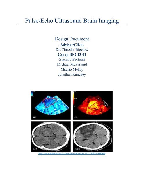
Pulse-Echo Ultrasound Brain Imaging - Senior Design
Pulse-Echo Ultrasound Brain Imaging - Senior Design
Pulse-Echo Ultrasound Brain Imaging - Senior Design

Create successful ePaper yourself
Turn your PDF publications into a flip-book with our unique Google optimized e-Paper software.
<strong>Pulse</strong>-<strong>Echo</strong> <strong>Ultrasound</strong> <strong>Brain</strong> <strong>Imaging</strong><br />
<strong>Design</strong> Document<br />
Advisor/Client<br />
Dr. Timothy Bigelow<br />
Group DEC13-01<br />
Zachary Bertram<br />
Michael McFarland<br />
Maurio Mckay<br />
Jonathan Runchey<br />
http://www.sciencedirect.com/science/article/pii/S2211968X12000484
April 28, 2013 DESIGN DOCUMENT<br />
Table of Contents<br />
Executive Summary pg. 3<br />
System Requirements pg. 3<br />
System Overview pg. 3<br />
Transmit Circuit pg. 4<br />
Receive Circuit pg. 5<br />
Computer Interface pg. 5<br />
Detailed System <strong>Design</strong> pg. 3<br />
Transducer pg. 6<br />
Computer Interface System pg. 6<br />
Beamformer pg. 7<br />
High Voltage <strong>Pulse</strong>r pg. 8<br />
T/R Switch pg. 10<br />
Low Noise Amplifier pg. 11<br />
Switch Bank pg. 12<br />
Board Break Down pg. 12<br />
Testing pg. 14<br />
Budget pg. 17<br />
DEC13-01 | <strong>Ultrasound</strong> <strong>Brain</strong> <strong>Imaging</strong> 2
April 28, 2013 DESIGN DOCUMENT<br />
Executive Summary<br />
The goal of this project is to expand upon a previous group’s design for a pulse echo ultrasound<br />
system for brain imaging, which could be used as a low cost alternative to fMRI. The following<br />
report will contain the design for a transmission circuit and a receive circuit for the ultrasound<br />
system. The transmit circuit will be able to send high voltage pulses (+/-50V) over 512 channels<br />
to a transducer. The receive circuit will then receive the signals from the transducer and amplify<br />
them before sending them to a computer interface.<br />
System Requirements<br />
Our goal is to design and build a transmit circuit capable of sending +/-50V pulses over 512<br />
channels to send to a 512 element transducer our client has previously bought. The circuit should<br />
then be capable of receiving low voltage pulses back from the transducer and amplifying them to<br />
send to the National Instruments DAQ system. To reduce costs our client wants us to<br />
demultiplex the signal from 512 channels to 128 channels before sending it to the National<br />
Instruments system.<br />
Functional<br />
■ Transmit 512 channels at 1.5 MHz<br />
■ Receive 128 channels<br />
■ Generate +/- 50 V bipolar pulses<br />
■ Protection for the receive circuitry<br />
■ Variable gain for differing imaging depths<br />
Non-functional<br />
■ Maximum 60 in 2 boards (to reduce cost)<br />
■ Circuitry housing<br />
■ Spacing optimization in complete machine to maintain accessibility<br />
System Overview<br />
We have divided our current design into three separate parts; transmit circuit, receive<br />
circuit, and the computer interface. The transmit and receive circuit are based on research from a<br />
previous group and suggested ultrasound hardware provided on the Texas Instruments website.<br />
A block diagram of the suggested Texas Instruments design can be seen below:<br />
DEC13-01 | <strong>Ultrasound</strong> <strong>Brain</strong> <strong>Imaging</strong> 3
April 28, 2013 DESIGN DOCUMENT<br />
Transmit Circuit:<br />
The transmit circuit will be responsible for sending +/-50V pulses to the transducer, using<br />
the LM96570 (beamformer) and LM96550(high voltage pulser). The control of the beamformer,<br />
and thusly the entire transmit circuit, is delegated to a National Instruments system specifically<br />
designed for use in ultrasound. The previous group’s design used high voltage pulsers, which<br />
were controlled by being connected directly to a computer interface and needed 18 control bits to<br />
be able to send pulses over 8 channels. To help keep costs down we decided to go with Texas<br />
Instrument’s suggestion of using the LM series combination of the LM96570 and LM96550. The<br />
extra addition of the beamformer IC allows us to control the pulser using a serial interface, which<br />
reduces the required control bits from 18 down to 9. Below is a block diagram representation of<br />
the transmit circuit:<br />
DEC13-01 | <strong>Ultrasound</strong> <strong>Brain</strong> <strong>Imaging</strong> 4
April 28, 2013 DESIGN DOCUMENT<br />
Receive Circuit:<br />
The receive circuit will be responsible for receiving the low voltage signals sent back by<br />
the transducer. The receive circuit will amplify and demultiplex the signal down to 128-channels<br />
(from 512 channels) before sending the information back to the computer interface. The receive<br />
circuit contains the TX810(T/R switch), the LMH6622 (Low Noise Amplifier or LNA), and the<br />
MAX14803 (analog switcher). The TX810 is responsible for protecting the receive circuitry<br />
from the high voltage pulses from the transmit circuit, by limiting its output voltage to 2Vpp. The<br />
low noise amplifier stage of the receive circuit is responsible for amplifying the low-voltage<br />
signal received back from the transducer, before it is sent to the analog switches. The analog<br />
switches are responsible for demultiplexing the signal from 512 channels to 128 channels.<br />
Below is a block diagram representation of the receive circuit:<br />
Computer Interface:<br />
To control our circuit we are going to be using a National Instruments PXI system which<br />
will be capable of sending control signals to our transmit and receive circuit. The National<br />
Instruments PXI system will contain the NI-5752 module, which contains a variable gain<br />
amplifier and analog to digital converter.<br />
DEC13-01 | <strong>Ultrasound</strong> <strong>Brain</strong> <strong>Imaging</strong> 5
April 28, 2013 DESIGN DOCUMENT<br />
Overall System Block Diagram:<br />
Detailed System <strong>Design</strong><br />
Transducer<br />
The transducer is the part of the system that will come in contact with the patient. It is able to<br />
receive a high voltage pulse which it then converts into an ultrasonic pulse at a pre-determined<br />
frequency. The ultrasonic pulse is then sent into the body and the reflected pulses are captured by<br />
the transducer and converted into electrical signals that can be processed to form images. We<br />
will be using a 512 element transducer in our design.<br />
Computer Interface System<br />
We will be using the National Instruments PXI System to receive the signals back from the<br />
transducer and to control our high voltage pulser. The PXI system has a modular design which<br />
allows us to different boards based on our needs. Our team will use the NI PXI-7813R Virtex-II<br />
3M Gate R Series Digital RIO Module to send control signals to the Beamformer. For the<br />
receive circuit we will be using the NI 5752 board.<br />
DEC13-01 | <strong>Ultrasound</strong> <strong>Brain</strong> <strong>Imaging</strong> 6
NI PXI-7813R:<br />
April 28, 2013 DESIGN DOCUMENT<br />
Parameter Specification Required<br />
Specification<br />
Digital Control<br />
Signals<br />
NI-5752:<br />
160 bits<br />
(will need 2)<br />
320 bits<br />
(64*5)<br />
Parameter Specification Required<br />
Specification<br />
Receive Channels 32 channels<br />
(we will need 4)<br />
Beamformer<br />
128 channels<br />
The Beamformer connects directly to the high voltage pulser and reduces the amount of digital<br />
signals needed to control the high voltage pulser from 18 to 9 channels.<br />
We will be using the Texas Instruments LM96570 Transmit Beamformer. It offers eight output P<br />
and N channels at an individual delay from .78 ns to 102.4 μs at a max pulse rate of 80 MHz.<br />
The National Instruments PXI system will send five control bits to the Beamformer which will<br />
then interpret these control bits and send the appropriate signal to the high voltage pulser to<br />
create a high voltage pulse over each of the 8 channels.<br />
DEC13-01 | <strong>Ultrasound</strong> <strong>Brain</strong> <strong>Imaging</strong> 7
High Voltage <strong>Pulse</strong>r<br />
April 28, 2013 DESIGN DOCUMENT<br />
Figure 1 LM 96570 Pin layout<br />
Figure 2 Reference Circuit<br />
The High Voltage <strong>Pulse</strong>r is the component of our system that will generate the excitations of the<br />
transducer. These excitations will be in the form of both positive and negative square pulses. It<br />
will be controlled by the LM96570 Beamformer.<br />
We will be using the Texas Instruments LM96550 <strong>Ultrasound</strong> Transmit <strong>Pulse</strong>r. As you may<br />
notice in the following table, we desire 512 channels of operation, but the LM96550 supplies<br />
only 8. Therefore, we will be using 64 pulsers in conjunction with one another to achieve the<br />
desired 512 channels.<br />
DEC13-01 | <strong>Ultrasound</strong> <strong>Brain</strong> <strong>Imaging</strong> 8
April 28, 2013 DESIGN DOCUMENT<br />
Parameter LM96550 Specification Required Specification<br />
Voltage Output +/- 50 V +/- 50 V<br />
Frequency Range Up to 15 MHz 1.5 MHz<br />
Number of Channels 8 512 (8x64)<br />
Switching Delay Time 32 ns Less than 167 ns<br />
Figure 3 LM96550 Pin Layout<br />
The pulser will only operate when the EN pin is driven HI. If the pulser is enabled, driving PIN<br />
or NIN HI will generate a positive or negative pulse, respectively, at Vout. Vout will be pulled<br />
to the positive supply (VPP) or the negative supply (VNN) by power MOSFETs. If both PIN<br />
and NIN are LO the output Vout will be pulled to GND (0 V). It is important to never drive both<br />
PIN and NIN HI as this will cause damage to the circuit. The following figure is a block<br />
diagram of a single channel of the pulser.<br />
DEC13-01 | <strong>Ultrasound</strong> <strong>Brain</strong> <strong>Imaging</strong> 9
T/R Switch<br />
April 28, 2013 DESIGN DOCUMENT<br />
Figure 4 Block diagram of single LM96550 channel<br />
The T/R switch will act as an interface between the transmit and the receive sides of our system.<br />
It will allow high-voltage signals from the High Voltage <strong>Pulse</strong>r to be passed to the transducer in<br />
the transmit stage, while limiting the output voltage to the receive stage to only 2Vpp Thus, the<br />
T/R switch’s primary purpose is to act as a buffer between the system’s Low Noise Amplifier<br />
and the High Voltage <strong>Pulse</strong>r as the Low Noise Amplifier can be permanently damaged by high<br />
voltages.<br />
We will be using the Texas Instruments TX810 part in our system. The TX810 supports 8<br />
channels and has three digital control bits (B1, B2, and B3) that determine its biasing current;<br />
increasing the biasing current decreases the switch’s impedance. Some properties of the system<br />
may be optimized by introducing different values of load inductance and resistance, but this may<br />
also lower the system’s sensitivity. We will determine what values we will use once sufficient<br />
testing has taken place.<br />
DEC13-01 | <strong>Ultrasound</strong> <strong>Brain</strong> <strong>Imaging</strong> 10
Low Noise Amplifier<br />
April 28, 2013 DESIGN DOCUMENT<br />
Figure 5 TX810 Pin Layout<br />
Figure 6 Block diagram of single TX810 channel<br />
The low noise amplifier amplifies the heavily attenuated, reflected signals from the transducer<br />
which have been transmitted through the T/R switch (TX810) such that the signals can be<br />
sampled and processed for imaging.<br />
For the low noise amplifier we chose to go with the LMH6622 from Texas Instruments.<br />
For our design our client estimated we would need to have 40dB worth of gain before sending<br />
the receive signal to the NI-5752 device. He was also looking for a 3dB bandwidth around<br />
DEC13-01 | <strong>Ultrasound</strong> <strong>Brain</strong> <strong>Imaging</strong> 11
April 28, 2013 DESIGN DOCUMENT<br />
10MHz to accomplish this we decided to go with two LMH6622 amplifiers in series. The reason<br />
for this was so that we could reach the required gain of 40dB and still have a 3dB bandwidth for<br />
each amplifier of at least 10 MHz.<br />
LNA Gain<br />
Parameter LMH6622 Specifications Required Specification<br />
N/A 40dB<br />
3dB Bandwidth N/A 10MHz<br />
Gaind Bandwidth 120MHz N/A<br />
Switch Bank<br />
In order to reduce how many NI 5752 boards we would need to buy, we decided to use<br />
Max14802 switch banks to multiplex our receive signal from 512 channels down to 128 channels.<br />
Parameter: MAX14802 Specifications: Desired Value:<br />
Number of Available Switches 16 integrated SPST switches An integrated array of 16-32<br />
switches<br />
Serial Interface Each device features a 20 MHz<br />
serial interface that operates at<br />
5V. Serial interfaces between<br />
devices can be daisy-chained for<br />
simplified control.<br />
Board Break Down<br />
“Latch Enable” pins control<br />
whether the devices retains its<br />
currently programmed state or<br />
loads a new state in.<br />
The device will feature an<br />
interface that will allow for each<br />
switch to be controlled<br />
individually.<br />
To save money our group plans on limiting ourselves to 60 in 2 for all printed circuit<br />
board designs. The reason for this is that senior design groups at Iowa State receive a discount on<br />
DEC13-01 | <strong>Ultrasound</strong> <strong>Brain</strong> <strong>Imaging</strong> 12
April 28, 2013 DESIGN DOCUMENT<br />
printed circuit boards under 60 in 2 . To accomplish this task we plan on dividing our circuit up<br />
into two separate groups as follows:<br />
Transmit/Receive Boards:<br />
The transmit/receive boards are responsible for transmitting the high voltage pulses to the<br />
transducer, and also receiving back the low voltage signal from the transducer. After receiving<br />
the low voltage signal from the transducer the circuit will amplify the low voltage signal before<br />
sending the amplified signal to the switch board. Below is a breakdown of how many parts will<br />
be needed for each 16 channel board.<br />
Switch Boards:<br />
Device Number of Devices per<br />
Board; 32 Boards Total<br />
LM96550 2<br />
LM96570 2<br />
TX810 2<br />
LMH6622 16<br />
The switch board will be responsible for de-multiplexing the signal down to 128 channels before<br />
sending the signal to the NI-5752 modules.<br />
Device Number of Devices per<br />
Board; 4 Boards Total<br />
Max1402 8<br />
DEC13-01 | <strong>Ultrasound</strong> <strong>Brain</strong> <strong>Imaging</strong> 13
April 28, 2013 DESIGN DOCUMENT<br />
Below is a block diagram demonstrating the interconnections between boards:<br />
Challenges Encountered<br />
● Learning Ultiboard/Multisim<br />
○ None of our group members had previous experience with Multisim, Ultiboard, or<br />
PCB design in general.<br />
● Understanding the previous group’s work<br />
○ We are continuing a previous senior design team’s work, and therefore had to put<br />
in a large amount of effort to understand their work and design. We also had to<br />
change a fair amount of their design in order to comply with updated<br />
requirements.<br />
● Finalizing our part set<br />
○ We also spent a large amount of time in choosing our parts. Initially we changed<br />
our high voltage pulser from a Hitachi part that the previous group had chosen to<br />
the current TI part, and ultimately, we chose an entirely new series of (TI) parts.<br />
Testing<br />
First Semester Test Plan<br />
For our first testing phase our group plans on designing and ordering an 8-channel test board<br />
containing the LM96570, LM96550, TX810, and eight LMH6622 chips. During the first phase<br />
of testing we want to show that we can both send and receive a signal using our planned chip set.<br />
DEC13-01 | <strong>Ultrasound</strong> <strong>Brain</strong> <strong>Imaging</strong> 14
April 28, 2013 DESIGN DOCUMENT<br />
We also want to make sure our circuit is compatible with the National Instruments system our<br />
client plans to order. Thus, we have designed our circuit to connect directly to the National<br />
Instruments system. Below is a schematic of the circuit we plan to test:<br />
Below is the PCB design of our 8-channel test board:<br />
DEC13-01 | <strong>Ultrasound</strong> <strong>Brain</strong> <strong>Imaging</strong> 15
April 28, 2013 DESIGN DOCUMENT<br />
Below is the I/O configuration of the test board:<br />
Input (NI-5752) Pin Name<br />
DI 0 BF sRD<br />
DI 1 HV_OTP<br />
DO 0 NC<br />
DO 1 BF_TX_EN<br />
DO 2 NC<br />
DO 3 BF_RST<br />
DO 4 NC<br />
DO 5 BF_sLE<br />
DO 6 HV_MODE<br />
DO 7 BF_sWR<br />
DO 8 HV_EN<br />
DO 9 BF_sCLK<br />
DO 10 T/R_B1<br />
DO 11 NC<br />
DO 12 T/R_B2<br />
DO 13 NC<br />
DO 14 T/R_B3<br />
DO 15 BF_PLL_CLK+<br />
Output (NI-5752) Pin<br />
Name<br />
AI 0+ LNA4<br />
AI 1+ LNA5<br />
AI 2+ LNA3<br />
AI 3+ LNA6<br />
AI 4+ LNA2<br />
AI 5+ LNA7<br />
AI 6+ LNA1<br />
AI 7+ LNA8<br />
AI 8+ NC<br />
AI 9+ NC<br />
AI 10+ NC<br />
AI 11+ NC<br />
AI 12+ NC<br />
AI 13+ NC<br />
AI 14+ NC<br />
AI 15+ NC<br />
DEC13-01 | <strong>Ultrasound</strong> <strong>Brain</strong> <strong>Imaging</strong> 16
Budget<br />
April 28, 2013 DESIGN DOCUMENT<br />
This semester we had a senior design budget of $1000. The majority of our budget was used to purchase<br />
the parts needed for our 8-channel test board. Below is a breakdown of where our money was spent:<br />
DEC13-01 | <strong>Ultrasound</strong> <strong>Brain</strong> <strong>Imaging</strong> 17