

3D integrated circuit prototype dedicated to the ... - HAL - IN2P3
3D integrated circuit prototype dedicated to the ... - HAL - IN2P3
3D integrated circuit prototype dedicated to the ... - HAL - IN2P3

Create successful ePaper yourself
Turn your PDF publications into a flip-book with our unique Google optimized e-Paper software.
II. OMEGAPIX DESIGN<br />
OMEGAPIX <strong>circuit</strong> embeds 64x24 readout channels that<br />
have been developed <strong>to</strong> match very drastic requirements. In<strong>to</strong><br />
<strong>the</strong> first layer, called analogue tier, <strong>the</strong>re are <strong>the</strong> analogue part<br />
of <strong>the</strong> front-end cell, a block which performs <strong>the</strong> selection of<br />
<strong>the</strong> column and <strong>the</strong> bias. In<strong>to</strong> <strong>the</strong> o<strong>the</strong>r layer, called digital<br />
tier, <strong>the</strong>re is a shift register with a read logic in<strong>to</strong> each<br />
channel.<br />
A. Requirements<br />
Although one of goals of this first chip is <strong>to</strong> explore this<br />
new technology, as much <strong>the</strong> 130 nm CMOS process from<br />
Chartered as reliability and yield of <strong>3D</strong> devices from<br />
Tezzaron, requirements have been chosen in such a way <strong>the</strong>y<br />
go <strong>to</strong> <strong>the</strong> future likely requirements of <strong>the</strong> ATLAS upgrade<br />
Super LHC pixel project.<br />
So, we want <strong>to</strong> explore a new possibility <strong>to</strong> minimize <strong>the</strong><br />
pixel pitch down <strong>to</strong> 50x50 µm. Thus a readout array matching<br />
a new MPI-HLL plannar pixel sensor <strong>pro<strong>to</strong>type</strong> from Munich<br />
has been designed.<br />
Figure 2: pixel array sensor <strong>pro<strong>to</strong>type</strong><br />
Some specifications are given bellow:<br />
Channel size: 50x50 µm. The first limitation of <strong>the</strong> pixel<br />
size is currently <strong>the</strong> electronics readout area.<br />
Dissipation: 3 µW/ch. If we want <strong>to</strong> keep an equivalent<br />
power consumption after <strong>the</strong> pixel size shrinking, we have <strong>to</strong><br />
low drastically <strong>the</strong> power dissipation for each channel.<br />
Typically <strong>the</strong> consumption should be 2.4 µW/Ch <strong>to</strong> keep <strong>the</strong><br />
power density at 96 mW/cm². The power density has been<br />
low down <strong>to</strong> 80 mW/cm² (2 µW/ch) for <strong>the</strong> analogue tier and<br />
40 mW/cm² (1 µW/ch) for <strong>the</strong> digital tier.<br />
Noise: <strong>the</strong> IC has been designed <strong>to</strong> low <strong>the</strong> noise down <strong>to</strong><br />
100 e- and <strong>to</strong> be able <strong>to</strong> decrease <strong>the</strong> threshold down <strong>to</strong> 1000<br />
e-.<br />
B. Analogue Tier<br />
The analogue channel is divided in<strong>to</strong> three parts: <strong>the</strong><br />
preamplifier, <strong>the</strong> shaper with threshold tuning and <strong>the</strong><br />
discrimina<strong>to</strong>r.<br />
444<br />
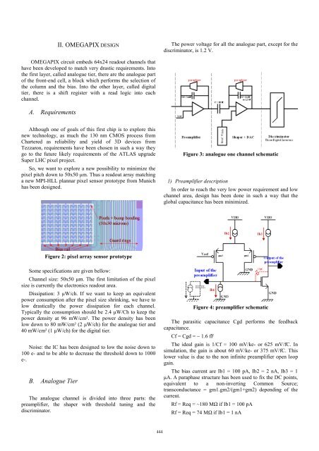
The power voltage for all <strong>the</strong> analogue part, except for <strong>the</strong><br />
discrimina<strong>to</strong>r, is 1.2 V.<br />
Figure 3: analogue one channel schematic<br />
1) Preamplifier description<br />
In order <strong>to</strong> reach <strong>the</strong> very low power requirement and low<br />
channel area, design has been done in such a way that <strong>the</strong><br />
global capacitance has been minimized.<br />
Figure 4: preamplifier schematic<br />
The parasitic capacitance Cgd performs <strong>the</strong> feedback<br />
capacitance.<br />
Cf = Cgd = ~ 1.6 fF<br />
The ideal gain is 1/Cf = 100 mV/ke- or 625 mV/fC. In<br />
simulation, <strong>the</strong> gain is about 60 mV/ke- or 375 mV/fC. This<br />
lower value is due <strong>to</strong> <strong>the</strong> non infinite preamplifier open loop<br />
gain.<br />
The bias current are Ib1 = 100 pA, Ib2 = 2 nA, Ib3 = 1<br />
µA. A paraphase structure has been used <strong>to</strong> fix <strong>the</strong> DC points,<br />
equivalent <strong>to</strong> a non-inverting Common Source;<br />
transconductance = gm1.gm2/(gm1+gm2) depending of <strong>the</strong><br />
current.<br />
Rf = Req = ~180 MΩ if Ib1 = 100 pA<br />
Rf = Req = 74 MΩ if Ib1 = 1 nA


![[tel-00433556, v1] Relation entre Stress Oxydant et Homéostasie ...](https://img.yumpu.com/19233319/1/184x260/tel-00433556-v1-relation-entre-stress-oxydant-et-homeostasie-.jpg?quality=85)