

3D integrated circuit prototype dedicated to the ... - HAL - IN2P3
3D integrated circuit prototype dedicated to the ... - HAL - IN2P3
3D integrated circuit prototype dedicated to the ... - HAL - IN2P3

Create successful ePaper yourself
Turn your PDF publications into a flip-book with our unique Google optimized e-Paper software.
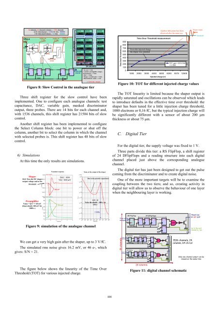
Chx.x<br />
in_test<br />
(1 bit)<br />
Ctest<br />
Vref<br />
From <strong>the</strong><br />
previous<br />
channel<br />
24 columns, 64 channels/columns -> 1536 channels<br />
14 SC bits/channel -> 21504 SC bits<br />
2 SC bits/selectColumn -> 48 bits<br />
D Q D Q D Q<br />
D Q D Q<br />
clock<br />
probe_pa<br />
(1 bit)<br />
5 bits<br />
4 bits<br />
Valid_mask<br />
(1 bit)<br />
probe_sh<br />
(1 bit)<br />
probe_d<br />
(1 bit)<br />
64 channels<br />
Ch1.64<br />
Ch1.4<br />
Ch1.3<br />
Ch1.2<br />
Ch1.1<br />
To <strong>the</strong> next<br />
channel<br />
Ch2.64<br />
Ch2.4<br />
Ch2.3<br />
Ch2.2<br />
Ch2.1<br />
24 columns<br />
Ch24.64<br />
Ch24.4<br />
Ch24.3<br />
Ch24.2<br />
Ch24.1<br />
sel1 sel2 sel24<br />
• In_test -> 1 bit<br />
• 3 probes: preamplifier, shaper,<br />
discrimina<strong>to</strong>r -> 3 bits<br />
• DAC -> 5 bits<br />
• Shaper: variable gain -> 4 bits<br />
• Discrimina<strong>to</strong>r: mask -> 1 bit<br />
-> 14 SC bits / channel<br />
Figure 8: Slow Control in <strong>the</strong> analogue tier<br />
Three shift register for <strong>the</strong> slow control have been<br />
implemented. One <strong>to</strong> configure each analogue channels: test<br />
capacitance, DAC, variable gain, masked discrimina<strong>to</strong>r<br />
output, three probes. There are 14 bits for each channel and,<br />
with 1536 channels, this shift register has 21504 bits of slow<br />
control.<br />
Ano<strong>the</strong>r shift register has been implemented <strong>to</strong> configure<br />
<strong>the</strong> Select Column block: one bit <strong>to</strong> power or shut off <strong>the</strong><br />
column, ano<strong>the</strong>r bit <strong>to</strong> select <strong>the</strong> column in which <strong>the</strong> channel<br />
with selected probes is. This shift register has 48 bits of slow<br />
control.<br />
6) Simulations<br />
At this time <strong>the</strong> only results are simulations.<br />
Shaper<br />
DAC fixes <strong>the</strong> DC shaper<br />
output voltage and so <strong>the</strong><br />
threshold<br />
Preamplifier<br />
Vmax = Q/C => 60 mV<br />
(<strong>the</strong>oretically 100 mV for<br />
1000 e-)<br />
Transient response<br />
282 mV<br />
DAC: 1000<br />
Vth = 800 mV<br />
59.6 mV<br />
Noise at <strong>the</strong> output of <strong>the</strong> shaper<br />
Due <strong>to</strong> <strong>the</strong> parasitic capacitance<br />
S/N = 8<br />
Noise threshold = 100 e- <strong>to</strong><br />
130 e-<br />
Figure 9: simulation of <strong>the</strong> analogue channel<br />
2 MHz<br />
We can get a very high gain after <strong>the</strong> shaper, up <strong>to</strong> 3 V/fC.<br />
The simulated rms noise gives 16.2 mV, or 46 e-, which<br />
gives: S/N = 21.<br />
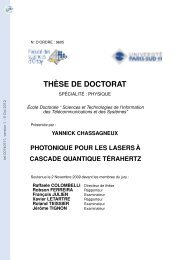
The figure below shows <strong>the</strong> linearity of <strong>the</strong> Time Over<br />
Threshold (TOT) for various injected charge.<br />
446<br />
Time Over Threshold (ns)<br />
900<br />
800<br />
700<br />
600<br />
500<br />
400<br />
300<br />
200<br />
100<br />
0<br />
Time Over Threshold measurement<br />
From this injected charge<br />
<strong>the</strong> shaper was saturated<br />
1000 2000 3000 4000 5000 6250 9375 12500<br />
Injected charge (e-)<br />
Ano<strong>the</strong>r little pulse has been<br />
observed after <strong>the</strong> main one<br />
TOT, gain = 0010, DAC<br />
= 0, 0000<br />
Shaper output<br />
Figure 10: TOT for different injected charge values<br />
threshold<br />
The TOT linearity is limited because <strong>the</strong> shaper output is<br />
rapidly saturated and oscillations can be observed which leads<br />
<strong>to</strong> introduce defaults in <strong>the</strong> effective time over threshold: <strong>the</strong><br />
shaper has been tuned for a little injection charge threshold,<br />
1000 electrons or 0,16 fC, but <strong>the</strong> typical injection charge will<br />
be significantly different with a sensor of about 200 µm<br />
thickness or about 75 µm.<br />
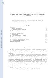
C. Digital Tier<br />
For <strong>the</strong> digital tier, <strong>the</strong> supply voltage was fixed <strong>to</strong> 1 V.<br />
Three parts divide this tier: a RS FlipFlop, a shift register<br />
of 24 DFlipFlops and a reading structure in<strong>to</strong> each digital<br />
channel placed just above <strong>the</strong> corresponding analogue<br />
channel.<br />
The digital tier has just been designed <strong>to</strong> get out <strong>the</strong> pulse<br />
coming from <strong>the</strong> discrimina<strong>to</strong>r and <strong>to</strong> create digital noise.<br />
One of <strong>the</strong> more important targets will be <strong>to</strong> examine <strong>the</strong><br />
coupling between <strong>the</strong> two tiers; and so, creating activity in<br />
digital tier will allow us <strong>to</strong> observe <strong>the</strong> behaviour of one layer<br />
when <strong>the</strong> neighbouring layer is working.<br />
From <strong>to</strong> <strong>the</strong><br />
analogue tier<br />
64 channels<br />
SR Flipflop<br />
RAZ<br />
SR Flipflop<br />
From <strong>to</strong> <strong>the</strong><br />
analogue tier S Q<br />
RAZ<br />
RN<br />
D Q D Q D Q D Q<br />
CLK (40 MHz)<br />
SR Flipflop<br />
From <strong>to</strong> <strong>the</strong><br />
analogue tier S Q<br />
RAZ<br />
RN<br />
D Q D Q D Q D Q<br />
CLK (40 MHz)<br />
S Q D Q D Q D Q D Q<br />
RN<br />
CLK (40 MHz)<br />
24 DFlipflops<br />
24 DFlipflops<br />
24 columns<br />
24 DFlipflops<br />
D_r<br />
CK_r<br />
D_r<br />
CK_r<br />
D Q<br />
D Q<br />
D_r<br />
CK_r<br />
NAND<br />
NAND<br />
D<br />
Q<br />
Q_r<br />
D_r<br />
Q_r<br />
D_r<br />
out<br />
NAND<br />
Q_r<br />
D_r<br />
1536 channels, 24<br />
columns, 64 ch/col<br />
Figure 11: digital channel schematic<br />
Read bus<br />
on out pad<br />
Go <strong>to</strong> <strong>the</strong> next<br />
channel D_r pin<br />
Only one channel output can be<br />
viewed on <strong>the</strong> same time

![[tel-00433556, v1] Relation entre Stress Oxydant et Homéostasie ...](https://img.yumpu.com/19233319/1/184x260/tel-00433556-v1-relation-entre-stress-oxydant-et-homeostasie-.jpg?quality=85)