CMOS Photoelectric Smoke Detector ASIC with ... - Microchip
CMOS Photoelectric Smoke Detector ASIC with ... - Microchip
CMOS Photoelectric Smoke Detector ASIC with ... - Microchip

You also want an ePaper? Increase the reach of your titles
YUMPU automatically turns print PDFs into web optimized ePapers that Google loves.
R&E International<br />
A Subsidiary of <strong>Microchip</strong> Technology Inc.<br />
RE46C140<br />
<strong>CMOS</strong> <strong>Photoelectric</strong> <strong>Smoke</strong> <strong>Detector</strong> <strong>ASIC</strong> <strong>with</strong> Interconnect and Timer Mode<br />
Product Specification<br />
General Description<br />
The RE46C140 is low power <strong>CMOS</strong> photoelectric type<br />
smoke detector IC. With minimal external components<br />
this circuit will provide all the required features for a<br />
photoelectric type smoke detector.<br />
The design incorporates a gain selectable photo<br />
amplifier for use <strong>with</strong> an infrared emitter/detector pair.<br />
An internal oscillator strobes power to the smoke<br />
detection circuitry for 100us every 10 seconds to keep<br />
standby current to a minimum. If smoke is sensed the<br />
detection rate is increased to verify an alarm condition.<br />
A high gain mode is available for push button chamber<br />
testing.<br />
A check for a low battery condition and chamber<br />
integrity is performed every 43 seconds when in<br />
standby. The temporal horn pattern supports the NFPA<br />
72 emergency evacuation signal.<br />
An interconnect pin allows multiple detectors to be<br />
connected such that when one units alarms, all units<br />
will sound.<br />
An internal 10 minute timer can be used for a reduced<br />
sensitivity mode.<br />
Utilizing low power <strong>CMOS</strong> technology the RE46C140<br />
was designed for use in smoke detectors that comply<br />
<strong>with</strong> Underwriters Laboratory Specification UL217 and<br />
UL268.<br />
Features<br />
• Internal Power On Reset<br />
• Low Quiescent Current Consumption<br />
• Available in 16L PDIP or 16L N SOIC<br />
• ESD Protection on all Pins<br />
• Interconnect up to 40 <strong>Detector</strong>s<br />
• 10 Minute Timer for Sensitivity Control<br />
• Temporal Horn Pattern<br />
• Internal Low Battery and Chamber Test<br />
• Compatible <strong>with</strong> Allegro A5366<br />
• Available in Standard Packaging or RoHS<br />
Compliant Pb Free Packaging.<br />
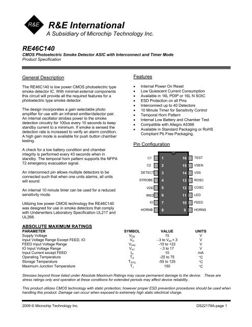
Pin Configuration<br />
2009 © <strong>Microchip</strong> Technology Inc. DS22179A-page 1<br />
C1<br />
1<br />
16<br />
C2 2<br />
15<br />
DETECT 3 14<br />
TEST<br />
VSEN<br />
VSS<br />
STROBE 4 13 ROSC<br />
ABSOLUTE MAXIMUM RATINGS<br />
PARAMETER SYMBOL VALUE UNITS<br />
Supply Voltage V DD 15 V<br />
Input Voltage Range Except FEED, IO V in -.3 to V dd +.3 V<br />
FEED Input Voltage Range V infd -10 to +22 V<br />
IO Input Voltage Range V io1 -.3 to 17 V<br />
Input Current except FEED I in 10 mA<br />
Operating Temperature T A -25 to 75 °C<br />
Storage Temperature T STG -55 to 125 °C<br />
Maximum Junction Temperature T J 150 °C<br />
Stresses beyond those listed under Absolute Maximum Ratings may cause permanent damage to the device. These are<br />
stress ratings only and operation at these conditions for extended periods may affect device reliability.<br />
This product utilizes <strong>CMOS</strong> technology <strong>with</strong> static protection; however proper ESD prevention procedures should be used when<br />
handling this product. Damage can occur when exposed to extremely high static electrical charge.<br />
VDD<br />
IRED<br />
IO<br />
HORNB<br />
5<br />
6<br />
7<br />
12<br />
11<br />
10<br />
8 9<br />
COSC<br />
LE D<br />
FEED<br />
HORNS
RE46C140<br />
<strong>CMOS</strong> <strong>Photoelectric</strong> <strong>Smoke</strong> <strong>Detector</strong> <strong>ASIC</strong> <strong>with</strong> Interconnect R&E International<br />
and Timer Mode A Subsidiary of <strong>Microchip</strong> Technology Inc.<br />
Product Specification<br />
DC Electrical Characteristics at TA = -25° to 75°C, VDD=9V, Typical Application (unless otherwise noted)<br />
Test<br />
Limits<br />
Parameter Symbol Pin Test Conditions Min Typ Max Units<br />
Supply Voltage VDD 5 Operating 6 12 V<br />
Supply Current<br />
IDD1 5<br />
Configured as in Figure 2,<br />
COSC=VSS, LED off<br />
4 6 uA<br />
IDD2 5<br />
Configured as in Figure 2, VDD=12V,<br />
COSC=VSS<br />
5.5 8 uA<br />
IDD3 5<br />
Configured as in Figure 2, STROBE<br />
on, IRED off, VDD=12V<br />
2 mA<br />
IDD4 5<br />
Configured as in Figure 2, STROBE<br />
on, IRED on, VDD=12V, Note 1<br />
3 mA<br />
Input Voltage High<br />
VIH1 10 FEED 6.2 4.5 V<br />
VIH2 7 No Local Alarm, IO as an Input 3.2 V<br />
VIH3 15 VSEN 1.6 V<br />
VIH4 16 TEST 8.5 V<br />
Input Voltage Low<br />
VIL1 10 FEED 4.5 2.7 V<br />
VIL2 7 No Local Alarm, IO as an Input 1.5 V<br />
VIL3 15 VSEN .5 V<br />
VIL4 16 TEST 7 V<br />
Input Leakage Low<br />
IIL1 1,2,3<br />
VDD=12V, COSC=12V, STROBE<br />
active<br />
-100 nA<br />
IIL2 12,10 VDD=12V, Vin=VSS -100 nA<br />
IIL3 15,16 VDD=12V, Vin=VSS -1 uA<br />
ILFD 10 FEED=-10V -50 uA<br />
Input Leakage High<br />
IIH1 1,2 VDD=12V, Vin=VDD, STROBE active 100 nA<br />
IIH2 3,12,10 VDD=12V, Vin=VDD 100 nA<br />
IHFD 10 FEED=22V 50 uA<br />
Input Pull Down Current IPD1 16 Vin=VDD .25 10 uA<br />
IPD2 15 Vin=VDD .1 .25 .5 uA<br />
IPDIO1 7 Vin=VDD 20 80 uA<br />
IPDIO2 7 Vin=17V, VDD=12 140 uA<br />
Output Leakage Current<br />
Low<br />
IOZL1 11,13 Output Off, Output=VSS -1 uA<br />
Output Leakage Current<br />
High<br />
IOZH1 11,13 Output Off, Output=VDD 1 uA<br />
Note 1: Does not include Q3 emitter current.<br />
2009 © <strong>Microchip</strong> Technology Inc. DS22179A-page 2
RE46C140<br />
<strong>CMOS</strong> <strong>Photoelectric</strong> <strong>Smoke</strong> <strong>Detector</strong> <strong>ASIC</strong> <strong>with</strong> Interconnect R&E International<br />
and Timer Mode A Subsidiary of <strong>Microchip</strong> Technology Inc.<br />
Product Specification<br />
DC Electrical Characteristics (continued) at TA= -25° to 75°, VDD=9V, Typical Application (unless<br />
otherwise noted)<br />
Test<br />
Limits<br />
Parameter Symbol Pin Test Conditions Min Typ Max Units<br />
Output Voltage Low<br />
VOL1 8,9 Iol=16mA, VDD=6.5V 1 V<br />
VOL2 13 Iol=5mA, VDD=6.5V .5 V<br />
VOL3 11 Iol=10mA, VDD=6.5V .6 V<br />
Output Voltage High VOh1 8,9 Iol=-16mA, VDD=6.5V 5.5 V<br />
Output Current<br />
IIOH1 7 Alarm, Vio=Vdd-2V or Vio=0V -4 -16 mA<br />
IIODMP 7<br />
At Conclusion of Local Alarm or<br />
Test, Vio=1V<br />
5 mA<br />
Low Battery Alarm Voltage VLB 5 6.9 7.2 7.5 V<br />
Output Voltage<br />
VSTOF 4<br />
STROBE off, VDD=12V,<br />
Iout=-1uA<br />
Vdd-.1 V<br />
VSTON 4<br />
STROBE on, VDD=9V<br />
Iout= 100uA to 500uA<br />
VDD -<br />
5.25<br />
VDD -<br />
5<br />
VDD -<br />
4.75<br />
V<br />
VIREDOF 6 IRED off, VDD=12V, Iout=1uA .1 V<br />
VIREDON 6<br />
IRED on, VDD=9V<br />
Iout=0 to -6mA, Ta=25C<br />
2.85 3.1 3.35 V<br />
Common Mode Voltage<br />
VCM1 1,2,3<br />
Local smoke, Push to Test or<br />
Chamber Test, Note 1<br />
.5 VDD-2 V<br />
<strong>Smoke</strong> Comparator<br />
Reference<br />
Vref - Internal Reference, Note 1<br />
VDD-<br />
3.7<br />
VDD- 3.3<br />
V<br />
Temperature Coefficient<br />
TCST 4<br />
VDD=6V to 12V, STROBE Output<br />
Voltage<br />
.01 %/ºC<br />
TCIRED 6<br />
VDD=6V to 12V, IRED Output<br />
Voltage<br />
.3 %/ºC<br />
Line Regulation<br />
ΔVSTON 4,5 Active, VDD=6V to 12V -50 dB<br />
ΔVIREDON 6,5 Active, VDD=6V to 12V -30 dB<br />
Note 1: Not production tested<br />
Typical values are for design information and are not guaranteed.<br />
Limits over the specified temperature range are not production tested and are based on characterization data.<br />
2009 © <strong>Microchip</strong> Technology Inc. DS22179A-page 3
RE46C140<br />
<strong>CMOS</strong> <strong>Photoelectric</strong> <strong>Smoke</strong> <strong>Detector</strong> <strong>ASIC</strong> <strong>with</strong> Interconnect R&E International<br />
and Timer Mode A Subsidiary of <strong>Microchip</strong> Technology Inc.<br />
Product Specification<br />
AC Electrical Characteristics at TA =-25° to 75°, VDD=9V, VSS=0V, Component Values from Figure 2 ;<br />
R9=100KΩ, R12=10MΩ, C5= 1.5nF(unless otherwise noted)<br />
Test<br />
Limits<br />
Parameter Symbol Pin Test Conditions Min Typ Max Units<br />
Oscillator Period TPOSC 12 No Alarm Condition 9.4 10.5 11.5 mS<br />
LED and STROBE On Time TON1 11,4 Operating 9.4 10.5 11.5 mS<br />
LED Period<br />
TPLED1 11 Standby, No Alarm 39 43 47 S<br />
TPLED2 11 Local Alarm Condition .45 .5 .55 S<br />
TPLED3 11 Timer Mode, No Local Alarm 9.6 10.75 11.8 S<br />
TPLED4 11 Remote Alarm Only LED IS NOT ON S<br />
STROBE and IRED Pulse<br />
Period<br />
TPER1 TPER1A 4,6<br />
4,6<br />
Standby, No Alarm<br />
Standby, After 1 Valid <strong>Smoke</strong><br />
Sample<br />
9.6<br />
1.8<br />
10.75<br />
2<br />
11.8<br />
2.2<br />
S<br />
S<br />
TPER1B 4,6<br />
Standby, After 2 Consecutive Valid<br />
<strong>Smoke</strong> Samples<br />
.9 1 1.1 S<br />
TPER2 4,6<br />
In Local Alarm – (3 Consecutive<br />
Valid <strong>Smoke</strong> Samples)<br />
.9 1 1.1 S<br />
TPER3 4,6 In Remote Alarm 7.2 8 8.9 S<br />
TPER4 4,6 Pushbutton Test 300 336 370 mS<br />
TPER5 4,6<br />
Chamber Test or Low Battery<br />
Test, no Alarms<br />
38.9 47.1 S<br />
IRED On Time TON2 6 Operating 94 104 115 uS<br />
Horn On Time<br />
THON1 8,9 Operating, Alarm Condition, Note 1 450 500 550 mS<br />
THON2 8,9<br />
Low Battery or Failed Chamber<br />
Test , No Alarm<br />
9.5 10.5 11.5 mS<br />
Horn Off Time<br />
THOF1 8,9 Operating, Alarm Condition, Note 1 450 500 550 mS<br />
THOF2 8,9 Operating, Alarm Condition, Note 1 1.35 1.5 1.65 S<br />
THOF3 8,9<br />
Low Battery or Failed Chamber<br />
Test, No Alarm<br />
39 43 47 S<br />
IO Charge Dump Duration<br />
TIODMP 7<br />
At Conclusion of Local Alarm or<br />
Test Alarm<br />
.9 1.46 S<br />
IO Delay<br />
TIODLY1 7<br />
From Start of Local Alarm to IO<br />
Active<br />
0 S<br />
IO Filter<br />
IO pulse width guaranteed to be<br />
TIOFILT 7 filtered. IO as Input, No Local<br />
Alarm<br />
600 mS<br />
Remote Alarm Delay<br />
TIODLY2 7<br />
No Local Alarm, From IO Active<br />
Horn Active<br />
1.05 2.0 S<br />
Timer Period TTPER No Alarm Condition, Note 2 8 10 12 Min<br />
Note 1 – See timing diagram for Horn Temporal Pattern<br />
Note 2 – During the timer mode the LED Period is 10.5 seconds. The LED period will return to a 43 seconds at the conclusion of the timer<br />
mode.<br />
Note 3 - T POSC and T ON2 are 100% production tested. All other timing is guaranteed by functional testing.<br />
Typical values are for design information and are not guaranteed.<br />
Limits over the specified temperature range are not production tested and are based on characterization data.<br />
2009 © <strong>Microchip</strong> Technology Inc. DS22179A-page 4
RE46C140<br />
<strong>CMOS</strong> <strong>Photoelectric</strong> <strong>Smoke</strong> <strong>Detector</strong> <strong>ASIC</strong> <strong>with</strong> Interconnect R&E International<br />
and Timer Mode A Subsidiary of <strong>Microchip</strong> Technology Inc.<br />
Product Specification<br />
2009 © <strong>Microchip</strong> Technology Inc. DS22179A-page 5
RE46C140<br />
<strong>CMOS</strong> <strong>Photoelectric</strong> <strong>Smoke</strong> <strong>Detector</strong> <strong>ASIC</strong> <strong>with</strong> Interconnect R&E International<br />
and Timer Mode A Subsidiary of <strong>Microchip</strong> Technology Inc.<br />
Product Specification<br />
Functional Block Diagram<br />
Figure 1<br />
2009 © <strong>Microchip</strong> Technology Inc. DS22179A-page 6
RE46C140<br />
<strong>CMOS</strong> <strong>Photoelectric</strong> <strong>Smoke</strong> <strong>Detector</strong> <strong>ASIC</strong> <strong>with</strong> Interconnect R&E International<br />
and Timer Mode A Subsidiary of <strong>Microchip</strong> Technology Inc.<br />
Product Specification<br />
PIN DESCRIPTIONS<br />
PIN# PIN NAME DESCRIPTION<br />
1 C1 The capacitor connected to this pin sets the photo amplifier gain (high) for the<br />
push-to-test and chamber sensitivity test. The size of this capacitor will depend<br />
on the chamber background reflections. A=1+(C1/10) where C1 is in pF. The<br />
gain should be
RE46C140<br />
<strong>CMOS</strong> <strong>Photoelectric</strong> <strong>Smoke</strong> <strong>Detector</strong> <strong>ASIC</strong> <strong>with</strong> Interconnect R&E International<br />
and Timer Mode A Subsidiary of <strong>Microchip</strong> Technology Inc.<br />
Product Specification<br />
Notes:<br />
Typical Application<br />
Figure 2<br />
1. C3 should be located as close as possible to the device power pins.<br />
2. C3 is typical for an alkaline battery. This capacitance should be increased to 4.7uF or greater for a carbon battery.<br />
3. R10, R11 and C6 are typical values and may be adjusted to maximize sound pressure.<br />
2009 © <strong>Microchip</strong> Technology Inc. DS22179A-page 8
RE46C140<br />
<strong>CMOS</strong> <strong>Photoelectric</strong> <strong>Smoke</strong> <strong>Detector</strong> <strong>ASIC</strong> <strong>with</strong> Interconnect R&E International<br />
and Timer Mode A Subsidiary of <strong>Microchip</strong> Technology Inc.<br />
Product Specification<br />
CIRCUIT DESCRIPTION AND APPLICATION NOTES<br />
Note: All timing references are nominal. See electrical characteristics for limits.<br />
Standby Internal Timing – With the external components specified in the typical application figure for ROSC and<br />
COSC the internal oscillator has a nominal period of 10mS. Normally the analog circuitry is powered down to<br />
minimize standby current (typically 4uA at 9V). Once every 10 seconds the detection circuitry (normal gain) is<br />
powered up for 10mS. Prior to completion of the 10mS period the IRED pulse is active for 100uS. At the<br />
conclusion of this 10mS period the photo amplifier is compared to an internal reference to determine the chamber<br />
status and latched. If a smoke condition is present the period to the next detection decreases and additional<br />
checks are made. Three consecutive smoke detections will cause the device to go into alarm and the horn circuit<br />
and interconnect will be active.<br />
Once every 40 seconds the status of the battery voltage is checked. This status is checked and latched at the<br />
conclusion of the LED pulse. In addition, once every 40 seconds the chamber is activated and using the high gain<br />
mode (capacitor C1) a check of the chamber is made by amplifying background reflections. If either the low<br />
battery or the photo chamber test fails the horn will chirp for 10mS every 40 seconds.<br />
The oscillator period is determined by the values of R9, R12 and C5 (see typical application FIG 2). The oscillator<br />
period T=TR+ TF where TR =.6931 * R12 * C5 and TF =.6931 * R9 * C5<br />
<strong>Smoke</strong> Detection Circuitry – A comparator compares the photo amp output to an internal reference voltage. If the<br />
required number of consecutive smoke conditions is met the device will go into local alarm and the horn will be<br />
active. In local alarm the C2 gain is internally increased by ~10% to provide alarm hysteresis.<br />
Push to Test Operation – If the TEST input pin is activated (Vih) then, after one internal clock cycle, the smoke<br />
detection rate increases to once every 330mS. In this mode the high gain capacitor C1 is selected and<br />
background reflections are used to simulate a smoke condition. After the required consecutive detections the<br />
device will go into a local alarm condition. When the TEST input is deactivated (Vil) and after one clock cycle the<br />
normal gain capacitor C1 is selected. The detection rate continues at once every 330mS until 3 consecutive no<br />
smoke conditions are detected. At this point the device returns to standby timing.<br />
LED Operation – In standby the LED is pulsed on for 10mS every 43 Seconds. In a local alarm condition or the<br />
push to test alarm the LED pulse frequency is increased to once every .5 seconds. In the case of a remote alarm<br />
the LED not active. In the timer mode of operation the LED is pulsed on for 10mS every 10 seconds.<br />
Interconnect Operation – The bidirectional IO pin allows for interconnection of multiple detectors. In a local alarm<br />
condition this pin is driven high immediately through a constant current source. Shorting this output to ground will<br />
not cause excessive current. The IO is ignored as an input during a local alarm.<br />
The IO pin also has an NMOS discharge device that is active for 1 second after the conclusion of any type of local<br />
alarm. This device helps to quickly discharge any capacitance associated <strong>with</strong> the interconnect line.<br />
If a remote active high signal is detected the device goes into remote alarm and the horn will be active. Internal<br />
protection circuitry allows for the signaling unit to have a higher supply voltage than the signaled unit <strong>with</strong>out<br />
excessive current draw.<br />
The interconnect input has a 670mS nominal digital filter. This allows for interconnection to other types of alarms<br />
(carbon monoxide for example) that may have a pulsed interconnect signal.<br />
2009 © <strong>Microchip</strong> Technology Inc. DS22179A-page 9
RE46C140<br />
<strong>CMOS</strong> <strong>Photoelectric</strong> <strong>Smoke</strong> <strong>Detector</strong> <strong>ASIC</strong> <strong>with</strong> Interconnect R&E International<br />
and Timer Mode A Subsidiary of <strong>Microchip</strong> Technology Inc.<br />
Product Specification<br />
Low Battery and Chamber Test – In standby an internal reference is compared to the voltage divided VDD supply.<br />
Low battery status is latched at the conclusion of the LED pulse. The horn will chirp for 10ms every 43 seconds<br />
until the low battery condition no longer exists. In standby a chamber test is also performed every 40 seconds by<br />
switching to the high gain capacitor C1 and sensing the photo chamber background reflections. Two consecutive<br />
chamber tests failures will also cause the horn to chirp for 10mS every 43 seconds. The low battery chirp occurs<br />
next to the LED pulse and the failed chamber test chirp ~20 seconds later. The low battery and chamber tests are<br />
not performed in a local or remote alarm condition.<br />
Timer Mode – If resistors Radj1 and Radj2 are in place and a high to low transition occurs on the TEST input the<br />
device enters a 10 minute timer mode. In this mode the smoke comparator reference is switched from the internal<br />
VDD-3.5V reference to the voltage that appears on VSEN (pin 15). This allows the sensitivity to be modified for<br />
the duration of the 10 minute timer period. The chamber test is performed in the timer mode. If VSEN is left<br />
unconnected or tied to VSS the timer mode of operation is inhibited.<br />
Diagnostic Mode – In addition to the normal function of the TEST input a special diagnostic mode is available for<br />
calibration and test of the smoke detector. Taking the TEST pin below VSS and sourcing ~300uA out of the pin<br />
for 1 clock cycle will enable the diagnostic mode. In the diagnostic mode some of the pin functions are redefined.<br />
Refer to the table below for redefined pin functions in the diagnostic mode. In addition in this mode STROBE is<br />
always enabled and the IRED is pulsed at the clock rate of 10.5mS nominal.<br />
Pin Name Pin Number Description<br />
IO 7 Disabled as an output. A high on this pin directs the photo amplifier output to pin C1<br />
(1) or C2 (2), determined by the level on VSEN (15). Amplification occurs during the<br />
IRED active time.<br />
VSEN 15 If IO is high then this pin controls the gain capacitor that is used. If VSEN is low then<br />
normal gain is selected and the photo amp output appears on C1 (1). If VSEN is<br />
high then high gain is selected and the photo amp output is on C2 (2).<br />
FEED 10 If VSEN (15) is low then taking this input high will enable hysteresis which is a<br />
nominal 10% gain increase in normal gain mode.<br />
COSC 12 If desired this pin can be driven by an external clock.<br />
HORNB 8 This pin becomes the smoke integrator output. A high level indicates that an alarm<br />
condition has been detected.<br />
LED 11 The LED pin is used as a low battery indicator. For VDD above the low battery<br />
threshold the open drain NMOS is off. If VDD falls below the threshold the NMOS<br />
turns on.<br />
2009 © <strong>Microchip</strong> Technology Inc. DS22179A-page 10
RE46C140<br />
<strong>CMOS</strong> <strong>Photoelectric</strong> <strong>Smoke</strong> <strong>Detector</strong> <strong>ASIC</strong> <strong>with</strong> Interconnect R&E International<br />
and Timer Mode A Subsidiary of <strong>Microchip</strong> Technology Inc.<br />
Product Specification<br />
Oscillator<br />
Internal Clock<br />
STROBE<br />
IRED<br />
LED<br />
LED<br />
Horn<br />
T POSC<br />
T PWOSC<br />
T ON1<br />
Timing Diagrams<br />
Standby, No Alarm (not to Scale)<br />
T ON2<br />
T PLED1<br />
T PER1<br />
Low Supply or Chamber Test Failure<br />
Low BatteryTest T HON3<br />
Low BatteryWarning Chirp Low Battery Warning Chirp<br />
Chamber Test and Warning is Offset from Low Battery Test and Warning by 21.5 Seconds.<br />
T HOF3<br />
2009 © <strong>Microchip</strong> Technology Inc. DS22179A-page 11
RE46C140<br />
<strong>CMOS</strong> <strong>Photoelectric</strong> <strong>Smoke</strong> <strong>Detector</strong> <strong>ASIC</strong> <strong>with</strong> Interconnect R&E International<br />
and Timer Mode A Subsidiary of <strong>Microchip</strong> Technology Inc.<br />
Product Specification<br />
STROBE<br />
IRED<br />
LED<br />
Horn<br />
IO as Output<br />
IO as Input<br />
T IOFILT<br />
T PER2<br />
T PLED2<br />
Timing Diagrams (continued)<br />
Local Alarm Timing (not to scale)<br />
No Alarm Local or Remote Alarm No Alarm<br />
T IODLY1<br />
Horn Temporal Pattern<br />
T HON1 T HOF1 T HOF2<br />
T IODLY2<br />
Interconnect Timing<br />
Notes:<br />
1. <strong>Smoke</strong> is not sampled when the horn is active. Horn cycle is self completing in local alarm but not in remote alarm.<br />
2. Low battery warning chirp is suppressed in local or remote alarm.<br />
3. IO Dump active only in local alarm, inactive if external alarm.<br />
2009 © <strong>Microchip</strong> Technology Inc. DS22179A-page 12
RE46C140<br />
<strong>CMOS</strong> <strong>Photoelectric</strong> <strong>Smoke</strong> <strong>Detector</strong> <strong>ASIC</strong> <strong>with</strong> Interconnect R&E International<br />
and Timer Mode A Subsidiary of <strong>Microchip</strong> Technology Inc.<br />
Product Specification<br />
Information contained in this publication regarding device<br />
applications and the like is provided only for your convenience and<br />
may be superseded by updates. It is your responsibility to ensure<br />
that your application meets <strong>with</strong> your specifications. MICROCHIP<br />
MAKES NO REPRESENTATIONS OR WARRANTIES OF ANY<br />
KIND WHETHER EXPRESS OR IMPLIED, WRITTEN OR ORAL,<br />
STATUTORY OR OTHERWISE, RELATED TO THE<br />
INFORMATION, INCLUDING BUT NOT LIMITED TO ITS<br />
CONDITION, QUALITY, PERFORMANCE, MERCHANTABILITY<br />
OR FITNESS FOR PURPOSE. <strong>Microchip</strong> disclaims all liability<br />
arising from this information and its use. Use of <strong>Microchip</strong> devices in<br />
life support and/or safety applications is entirely at the buyer’s risk,<br />
and the buyer agrees to defend, indemnify and hold harmless<br />
<strong>Microchip</strong> from any and all damages, claims, suits, or expenses<br />
resulting from such use. No licenses are conveyed, implicitly or<br />
otherwise, under any <strong>Microchip</strong> intellectual property rights.<br />
Trademarks<br />
The <strong>Microchip</strong> name and logo, the <strong>Microchip</strong> logo, Accuron,<br />
dsPIC, KEELOQ, KEELOQ logo, MPLAB, PIC, PICmicro,<br />
PICSTART, rfPIC, SmartShunt and UNI/O are registered<br />
trademarks of <strong>Microchip</strong> Technology Incorporated in the U.S.A.<br />
and other countries.<br />
FilterLab, Hampshire, Linear Active Thermistor, MXDEV, MXLAB,<br />
SEEVAL, SmartSensor and The Embedded Control Solutions<br />
Company are registered trademarks of <strong>Microchip</strong> Technology<br />
Incorporated in the U.S.A.<br />
Analog-for-the-Digital Age, Application Maestro, CodeGuard,<br />
dsPICDEM, dsPICDEM.net, dsPICworks, dsSPEAK, ECAN,<br />
ECONOMONITOR, FanSense, In-Circuit Serial Programming,<br />
ICSP, ICEPIC, Mindi, MiWi, MPASM, MPLAB Certified logo,<br />
MPLIB, MPLINK, mTouch, nanoWatt XLP, PICkit, PICDEM,<br />
PICDEM.net, PICtail, PIC 32 logo, PowerCal, PowerInfo,<br />
PowerMate, PowerTool, REAL ICE, rfLAB, Select Mode, Total<br />
Endurance, TSHARC, WiperLock and ZENA are trademarks of<br />
<strong>Microchip</strong> Technology Incorporated in the U.S.A. and other<br />
countries.<br />
SQTP is a service mark of <strong>Microchip</strong> Technology Incorporated in<br />
the U.S.A.<br />
All other trademarks mentioned herein are property of their<br />
respective companies.<br />
© 2009, <strong>Microchip</strong> Technology Incorporated, Printed in the<br />
U.S.A., All Rights Reserved.<br />
Printed on recycled paper.<br />
<strong>Microchip</strong> received ISO/TS-16949:2002 certification for its worldwide<br />
headquarters, design and wafer fabrication facilities in Chandler and<br />
Tempe, Arizona; Gresham, Oregon and design centers in California and<br />
India. The Company’s quality system processes and procedures are for its<br />
PIC ® MCUs and dsPIC ® DSCs, KEELOQ ® code hopping devices, Serial<br />
EEPROMs, microperipherals, nonvolatile memory and analog products. In<br />
addition, <strong>Microchip</strong>’s quality system for the design and manufacture of<br />
development systems is ISO 9001:2000 certified.<br />
2009 © <strong>Microchip</strong> Technology Inc. DS22179A-page 13