Chapter 5
Chapter 5
Chapter 5

Create successful ePaper yourself
Turn your PDF publications into a flip-book with our unique Google optimized e-Paper software.
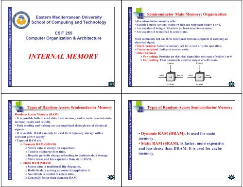
CSIT 255 Computer Organization & Architecture by Dr. Ali Hakan ULUSOY<br />
CSIT 255 Computer Organization & Architecture by Dr. Ali Hakan ULUSOY<br />
Eastern Mediterranean University<br />
School of Computing and Technology<br />
CSIT 255<br />
Computer Organization & Architecture<br />
INTERNAL MEMORY<br />
Types of Random-Access Semiconductor Memory<br />
ULUSOY<br />
Hakan Ali Dr. by Architecture & Organization Computer 255<br />
o No refresh is needed to retain data.<br />
o Generally faster than dynamic RAM. 3<br />
CSIT<br />
Random-Access Memory (RAM)<br />
• It is possible both to read data from memory and to write new data into<br />
memory easily and rapidly.<br />
• Both reading and writing are accomplished through use of electrical<br />
signals.<br />
• It is volatile. RAM can only be used for temporary storage with a<br />
constant power supply.<br />
• Types of RAM are<br />
Dynamic RAM (DRAM)<br />
o Stores data as charge on capacitors.<br />
o Tend to discharge over time.<br />
o Require periodic charge refreshing to maintain data storage.<br />
o More dense and less expensive than static RAM.<br />
Static RAM (SRAM)<br />
o Stores data in traditional flip-flop gates.<br />
o Holds its data as long as power is supplied to it.<br />
1<br />
CSIT 255 Computer Organization & Architecture by Dr. Ali Hakan ULUSOY<br />
Semiconductor Main Memory: Organization<br />
All semiconductor memory cells:<br />
• Exhibit 2 stable (or semi-stable) which can represent binary 1 or 0.<br />
• Are capable of being written into (at least once) to set states.<br />
• Are capable of being read to sense states.<br />
Most commonly cell has three functional terminals capable of carrying an<br />
electrical signal.<br />
• Select terminal. Selects a memory cell for a read or write operation.<br />
• Control terminal. Indicates read or write.<br />
• Other terminal<br />
For writing. Provides an electrical signal that sets state of cell to 1 or 0.<br />
For reading. That terminal is used for output of cell’s state.<br />
Types of Random-Access Semiconductor Memory<br />
• Dynamic RAM (DRAM). Is used for main<br />
memory.<br />
• Static RAM (SRAM). Is faster, more expensive<br />
and less dense than DRAM. It is used for cache<br />
memory.<br />
2<br />
4
CSIT 255 Computer Organization & Architecture by Dr. Ali Hakan ULUSOY<br />
CSIT 255 Computer Organization & Architecture by Dr. Ali Hakan ULUSOY<br />
Structure of Dynamic RAM (DRAM)<br />
ULUSOY<br />
Address line is activated when bit value<br />
from this cell is to be read or written.<br />
Hakan Ali Dr.<br />
Transistor acts as a switch that is<br />
by<br />
• closed (allowing current to flow) if a<br />
voltage is applied to address line.<br />
• open (no current flows) if no voltage is<br />
present on address line.<br />
Architecture &<br />
For write operation, a voltage signal is applied to bit line (high<br />
voltage=1 and low voltage=0). A signal is then applied to address line,<br />
allowing a charge to be transferred to capacitor.<br />
Organization<br />
For read operation, when address line is selected, transistor turns on<br />
and charge stored on capacitor is fed out onto a bit line and to a sense<br />
Computer<br />
amplifier. Sense amplifier compares capacitor voltage to a reference<br />
255<br />
value and determines if cell contains logic 1 or o. Read out from cell<br />
discharges capacitor, which must be restored to complete operation. 5<br />
CSIT<br />
Read-Only Memory (ROM)<br />
Read-Only Memory (ROM)<br />
• Contains a permanent pattern of data which can not be<br />
changed.<br />
• Is nonvolatile. No power source is required to maintain<br />
bit values in memory.<br />
• While it is possible to read a ROM, it is not possible to<br />
write new data into it.<br />
• Data is actually wired in to chip as part of fabrication<br />
process. This presents two problems:<br />
Data insertion step has a large fixed cost.<br />
No room for error. If one bit is wrong, whole set of<br />
ROMs must be thrown out.<br />
7<br />
CSIT 255 Computer Organization & Architecture by Dr. Ali Hakan ULUSOY<br />
Structure of Static RAM (SRAM)<br />
Four transistors (T 1, T 2, T 3, T 4) produces a<br />
stable logical state.<br />
In logic state 1, point C 1 is high and point C 2<br />
is low; in this state, T 1 and T 4 are off and T 2<br />
and T 3 are on.<br />
In logic state 0, point C 1 is low and point C 2<br />
is high; in this state, T 1 and T 4 are on and T 2<br />
and T 3 are off.<br />
Both state are stable as long as direct current (dc) voltage is applied.<br />
Address line is used to open or close a switch. Address line controls two<br />
transistors (T 5 and T 6). When a signal is applied to this line, two transistors<br />
are switched on. Allowing a read or write operation.<br />
For a write operation, desired bit value is applied to line B forcing T1, T2, T3, T4 to proper states. For a read operation, bit value is read from line B.<br />
Types of Read-Only Memory (ROM)<br />
Types of Read-Only Memory (ROM)<br />
• Programmable ROM (PROM)<br />
• Erasable programmable ROM (EPROM)<br />
• Electrically erasable programmable<br />
(EEPROM)<br />
6<br />
8
CSIT 255 Computer Organization & Architecture by Dr. Ali Hakan ULUSOY<br />
CSIT 255 Computer Organization & Architecture by Dr. Ali Hakan ULUSOY<br />
Types of Read-Only Memory (ROM)<br />
Programmable Read-Only Memory (PROM)<br />
• Writing process is performed<br />
Electrically.<br />
By a supplier or customer after chip<br />
fabrication.<br />
• Special equipment is required for writing or<br />
programming process.<br />
• Is nonvolatile and may be written into only once.<br />
Types of Read-Only Memory (ROM)<br />
Electrically Erasable Programmable Read-Only<br />
Memory (EEPROM)<br />
• Any part of memory can be written at any time<br />
without erasing prior contents.<br />
• Updateable in place using ordinary bus control,<br />
address and data lines.<br />
• Is nonvolatile.<br />
• Writing takes much longer than reading.<br />
• More expensive and less dense than EPROM.<br />
9<br />
11<br />
CSIT 255 Computer Organization & Architecture by Dr. Ali Hakan ULUSOY<br />
CSIT 255 Computer Organization & Architecture by Dr. Ali Hakan ULUSOY<br />
Types of Read-Only Memory (ROM)<br />
Erasable Programmable Read-Only Memory<br />
(EPROM)<br />
• Read and write electrically, as with PROM.<br />
• Before a write, all cells must be erased by exposure<br />
to ultraviolet radiation (erasure takes about 20<br />
minutes).<br />
• Writing uses different electronics than normal<br />
memory writes.<br />
• Is nonvolatile.<br />
• Errors can be corrected by erasing and starting<br />
over.<br />
• More expensive than PROM.<br />
Types of Random-Access Semiconductor Memory<br />
Flash Memory<br />
• Uses electrical erasing technology.<br />
• Much faster erasure than EPROM.<br />
• Same density as EPROM.<br />
• Allows individual blocks to be erased rather than<br />
an entire chip.<br />
• Gets its name because microchip is organized so<br />
that a section of memory cells are erased in a single<br />
action or “flash”.<br />
10<br />
12
CSIT 255 Computer Organization & Architecture by Dr. Ali Hakan ULUSOY<br />
CSIT 255 Computer Organization & Architecture by Dr. Ali Hakan ULUSOY<br />
Types of Random-Access Semiconductor Memory<br />
Typical 16M DRAM (4M × 4)<br />
13<br />
15<br />
CSIT 255 Computer Organization & Architecture by Dr. Ali Hakan ULUSOY<br />
CSIT 255 Computer Organization & Architecture by Dr. Ali Hakan ULUSOY<br />
Semiconductor Main Memory: Chip Logic<br />
Each chip contains an array of memory cells.<br />
For semiconductor memories, one of key design issues is number of bits<br />
of data that may be read/written at a time:<br />
• Physical organization is same as logical organization is one extreme.<br />
Array is organized into W words of B bits each.<br />
• Other extreme is 1-bit-per-chip. Data is read/written one bit at a time.<br />
Typical organization of a 16Mbit DRAM<br />
• 4 bits are read/written at a time.<br />
• Logically, memory array is organized as 4 square arrays of 2048×2048<br />
elements.<br />
• Horizontal lines connect to Select terminal of each cell in its row.<br />
• Vertical lines connect to Data-In/Sense terminals of each cell in its<br />
column.<br />
• 11 address lines are needed to select one of 2048 rows and 11 address<br />
lines are needed to select one of 2048 columns (2 11 = 2048).<br />
• Multiple DRAMs must be connected to memory controller to<br />
read/write an 8 bit word.<br />
Semiconductor Main Memory: Chip Packaging<br />
An integrated circuit is mounted on a package that contains pins for<br />
connection to outside world.<br />
Typical pinouts of EPROM package, which is<br />
an 8-Mbit chip organization as 1M × 8:<br />
• A0-A19: Address of word being accessed. For<br />
1M words, 20 pins are needed (2 20 = 1M).<br />
• D0-D7: Data to be read out.<br />
• Vcc: Power supply to chip.<br />
• Vss: A ground pin.<br />
• CE: Chip enable which is used to indicate<br />
whether or not address is valid for this chip.<br />
• Vpp: Program voltage which is used for<br />
writes to (programming) an EPROM.<br />
14<br />
16
CSIT 255 Computer Organization & Architecture by Dr. Ali Hakan ULUSOY<br />
CSIT 255 Computer Organization & Architecture by Dr. Ali Hakan ULUSOY<br />
Semiconductor Main Memory: Chip Packaging<br />
Typical pinouts of DRAM for a 16-Mbit chip<br />
organized as 4M × 4:<br />
• A0-A10: Address of word being accessed.<br />
DRAM is accessed by row and column and<br />
address is multiplexed, only 11 pins are<br />
needed to satisfy 4M row/column<br />
combinations (2 11 ×2 11 = 2 22 =4M).<br />
• D1-D4: Data to be read out.<br />
• Vcc: Power supply to chip.<br />
• Vss: A ground pin.<br />
• RAS: Row address select.<br />
• CAS: Column address select.<br />
• W or WE: Write enable for write operation.<br />
• OE: Output enable for read operation.<br />
• NC: No connection.<br />
Module Organization<br />
In case in which larger memory is required, an array of chips is needed.<br />
Example shows possible organization of a memory consisting of 1M word by 8<br />
bits per word. In this case, we have four columns of chips, each column<br />
containing 256K words arranged as follows:<br />
17<br />
19<br />
CSIT 255 Computer Organization & Architecture by Dr. Ali Hakan ULUSOY<br />
CSIT 255 Computer Organization & Architecture by Dr. Ali Hakan ULUSOY<br />
Module<br />
Organization<br />
If a RAM chip contains only 1<br />
bit per word, then clearly we<br />
will need at least a number of<br />
chips equal to number of bits<br />
per word.<br />
Example shows how a<br />
memory module consisting of<br />
256K 8-bit words can be<br />
organized.<br />
For 256K words, an 18-bit<br />
address is needed.<br />
Error Correction<br />
A semiconductor memory is subject to errors.<br />
These errors can categorized as<br />
• Hard Failure. Is a permanent physical defect so that<br />
memory cell or cells affected cannot reliably store data.<br />
• Soft Error. A random, nondestructive event that alters<br />
contents of one or more memory cells, without damaging<br />
memory. Soft errors can be caused by:<br />
Power supply problems.<br />
Alpha particles which result from radioactive decay.<br />
Both hard and soft errors are clearly undesirable and most<br />
modern main memory systems include logic for both<br />
detecting and correcting errors.<br />
18<br />
20
CSIT 255 Computer Organization & Architecture by Dr. Ali Hakan ULUSOY<br />
CSIT 255 Computer Organization & Architecture by Dr. Ali Hakan ULUSOY<br />
Error Correction<br />
When data are to be read into memory, a calculation (f) is<br />
performed on data to produce a code.<br />
Both code and data are stored.<br />
For M-bit word and K-bit code, actual size of stored word is<br />
M+K.<br />
When previously stored word is read out, code is used to<br />
detect and possibly correct errors.<br />
A new set of K code bits is generated from M data bits and<br />
compared with fetched code bits.<br />
Error Correction<br />
ULUSOY<br />
An error-correcting code is<br />
characterized by number of bit<br />
Hakan Ali<br />
errors in a word that it can correct<br />
and detect.<br />
Dr. by<br />
The simplest of error-correcting<br />
codes is Hamming code.<br />
Architecture &<br />
For example, a hamming code for 4<br />
data bits (1110) requires 3 parity<br />
bits (100), as shown (to make<br />
number of 1s in a circle even).<br />
Organization<br />
Note that the parity bits (10) are<br />
now incorrect, and their<br />
Computer<br />
intersection identifies the data bit in<br />
255<br />
error, which can be<br />
corrected back to (1) by negation. 23<br />
CSIT<br />
21<br />
CSIT 255 Computer Organization & Architecture by Dr. Ali Hakan ULUSOY<br />
Error Correction<br />
Comparison yields one of three results:<br />
• No errors are detected. Fetched data bits are sent out.<br />
• An error is detected and it is possible to correct error.<br />
• An error is detected, but it is not possible to correct it.<br />
Codes that operate in this fashion are referred to as errorcorrecting<br />
codes.<br />
Error Correction<br />
To clarify concepts involved, we will develop a code that<br />
can detect and correct single-bit errors in 8-bit word.<br />
Determine how long code must be by<br />
2 K -1 ≥ M + K<br />
where M: length of data.<br />
K: length of check bits.<br />
For example, for a word of 8 data bits (M=8), we have<br />
• K=3: 2 3 -1 < 8+3<br />
• K=4:2 4 -1 > 8+4<br />
8 data bits require 4 check bits.<br />
22<br />
24
CSIT 255 Computer Organization & Architecture by Dr. Ali Hakan ULUSOY<br />
CSIT 255 Computer Organization & Architecture by Dr. Ali Hakan ULUSOY<br />
Error Correction<br />
Following table shows number of bits required for<br />
various data word lengths:<br />
Error Correction<br />
Check bits are calculated as follows, where symbol ⊕<br />
designates exclusive-or operation:<br />
C1=<br />
C2=<br />
C4=<br />
C8=<br />
D1⊕<br />
D1⊕<br />
D2⊕<br />
D2⊕<br />
D3⊕<br />
D3⊕<br />
D4⊕<br />
D4⊕<br />
D4⊕<br />
D5⊕<br />
D5⊕<br />
D6⊕<br />
D6⊕<br />
D7⊕<br />
D8<br />
D8<br />
Each check bit operates on every data bit whose position<br />
number contains a 1 in same bit position as position number<br />
of that check bit.<br />
For example data bit positions 3, 5, 7, 9 and 11 (D1, D2, D4,<br />
D5, D7) all contain a 1 in the least significant bit of their<br />
position number as does C1; bit positions 3, 6, 7, 10 and 11<br />
all contain a 1 in second bit position, as does C2 and so on.<br />
D7<br />
D7<br />
P<br />
0<br />
0<br />
1<br />
1<br />
Q<br />
0<br />
1<br />
0<br />
1<br />
P XOR Q<br />
0<br />
1<br />
1<br />
0<br />
25<br />
27<br />
CSIT 255 Computer Organization & Architecture by Dr. Ali Hakan ULUSOY<br />
CSIT 255 Computer Organization & Architecture by Dr. Ali Hakan ULUSOY<br />
Error Correction<br />
To find position of error and correct it, data and bits are<br />
arranged into a 12-bit word.<br />
Bit positions are numbered from 1 to 12.<br />
Those bit positions whose position numbers are powers<br />
of 2 are designated as check bits.<br />
Bit position<br />
Position number<br />
Data bit<br />
Check bit<br />
12<br />
1100<br />
D8<br />
11<br />
1011<br />
D7<br />
10<br />
1010<br />
D6<br />
9<br />
1001<br />
D5<br />
Error Correction<br />
8<br />
1000<br />
C8<br />
New and old check bits are compared by exclusive or<br />
operation:<br />
• If result contains all zero, no error has detected.<br />
• If result contains one and only one bit set to 1, then an<br />
error has occurred in one of the check bits. No correction<br />
is needed.<br />
• If result contains more then one bit set to 1, then<br />
numerical value of result indicates position of data bit in<br />
error. This data is inverted for correction.<br />
7<br />
0111<br />
D4<br />
6<br />
0110<br />
D3<br />
5<br />
0101<br />
D2<br />
4<br />
0100<br />
C4<br />
3<br />
0011<br />
D1<br />
2<br />
0010<br />
C2<br />
1<br />
0001<br />
C1<br />
26<br />
28
CSIT 255 Computer Organization & Architecture by Dr. Ali Hakan ULUSOY<br />
CSIT 255 Computer Organization & Architecture by Dr. Ali Hakan ULUSOY<br />
Error Correction<br />
Example: Assume that 8-bit input word is 00111001, with data bit D1 in rightmost<br />
position. Calculations are as:<br />
Bit position<br />
Data bit<br />
Input word<br />
8<br />
D8<br />
0<br />
7<br />
D7<br />
0<br />
6<br />
D6<br />
1<br />
5<br />
D5<br />
1<br />
4<br />
D4<br />
1<br />
3<br />
D3<br />
0<br />
2<br />
D2<br />
C1=D1 ⊕ D2 ⊕ D4 ⊕ D5 ⊕ D7 =1 ⊕ 0 ⊕ 1 ⊕ 1 ⊕ 0 =1<br />
C2=D1 ⊕ D3 ⊕ D4 ⊕ D6 ⊕ D7 =1 ⊕ 0 ⊕ 1 ⊕ 1 ⊕ 0 =1<br />
C4=D2 ⊕ D3 ⊕ D4 ⊕ D8 =0 ⊕ 0 ⊕ 1 ⊕ 0=1<br />
C8=D5 ⊕ D6 ⊕ D7 ⊕ D8 =1 ⊕ 1 ⊕ 0 ⊕ 0=0<br />
Suppose that data bit 3 sustains an error and is changed from 0 to 1. When check<br />
bits are recalculated, we have<br />
C1=D1 ⊕ D2 ⊕ D4 ⊕ D5 ⊕ D7 =1 ⊕ 0 ⊕ 1 ⊕ 1 ⊕ 0 =1<br />
C2=D1 ⊕ D3 ⊕ D4 ⊕ D6 ⊕ D7 =1 ⊕ 1 ⊕ 1 ⊕ 1 ⊕ 0 =0<br />
C4=D2 ⊕ D3 ⊕ D4 ⊕ D8 =0 ⊕ 1 ⊕ 1 ⊕ 0=0<br />
C8 C4 C2 C1<br />
C8=D5 ⊕ D6 ⊕ D7 ⊕ D8 =1 ⊕ 1 ⊕ 0 ⊕ 0=0<br />
0 1 1 1<br />
New check bits are compared with old check bits:<br />
Result is 0110, indicating that bit position 6 is in error.<br />
0<br />
Error Correction<br />
ULUSOY<br />
Hakan<br />
Assume a 4-bit data word.<br />
Ali Dr. by<br />
Sequence shows that if 2<br />
errors occur (c).<br />
Architecture<br />
Wrong bit mistakenly<br />
&<br />
corrected (e).<br />
To overcome problem, an eight bit is added that is set so that<br />
Organization<br />
total number of 1s in diagram is even.<br />
Extra parity bit catches error (f).<br />
Computer 255<br />
So detect bit is changed to 0, indicating error. 31<br />
CSIT<br />
1<br />
D1<br />
1<br />
⊕<br />
0<br />
0<br />
0<br />
1<br />
0<br />
1<br />
1<br />
0<br />
29<br />
CSIT 255 Computer Organization & Architecture by Dr. Ali Hakan ULUSOY<br />
Error Correction<br />
Code just described is known as a single-error-correcting<br />
(SEC) code.<br />
More commonly, semiconductor memory is equipped with a<br />
single-error-correcting, double-error-detecting (SEC-DED)<br />
code.<br />
Note that an error of more than a single bit cannot be<br />
corrected with the previous method.<br />
Instead, we can add an additional bit to make total number of<br />
1’s (in both data and parity bits) even. If this bit compares<br />
differently, we know that a double error has been detected<br />
(although we cannot correct it).<br />
Advanced DRAM Organization<br />
In recent years, a number of enhancements to basic DRAM<br />
architecture have been explored:<br />
• Synchronous DRAM (SDRAM)<br />
Standard DRAM is asynchronous.<br />
o Processor presents addresses and control levels to<br />
memory for read and write.<br />
o After a delay, access time, DRAM either writes or reads.<br />
o Processor must wait through this delay, slowing system<br />
performance.<br />
SDRAM moves data in and out in a set number of clock<br />
cycles, synchronized with system clock, just like processor.<br />
CPU does not have to wait, it can do something else.<br />
An enhanced version of SDRAM is known as double data<br />
rate SDRAM (DDR-SDRAM) which can send data to CPU<br />
twice per clock cycle.<br />
30<br />
32
CSIT 255 Computer Organization & Architecture by Dr. Ali Hakan ULUSOY<br />
CSIT 255 Computer Organization & Architecture by Dr. Ali Hakan ULUSOY<br />
Advanced DRAM Organization<br />
• Rambus DRAM (RDRAM)<br />
Vertical package, all pins on one side, designed to<br />
plug into RDRAM bus (a special high-speed bus just<br />
for memory).<br />
After initial 480 ns access time, provides burst<br />
speeds of 500 Mbps (compared with about 33Mbps<br />
for asynchronous DRAMs).<br />
Advanced DRAM Organization<br />
• Cache DRAM (CDRAM)<br />
Integrates a small SRAM cache (16 Kb) onto a<br />
basic DRAM chip.<br />
SRAM on CDRAM can be used in two ways:<br />
o Used as a true cache which is effective for<br />
ordinary random access to memory.<br />
o Used as a buffer to support serial access of a<br />
block of data.<br />
33<br />
35<br />
CSIT 255 Computer Organization & Architecture by Dr. Ali Hakan ULUSOY<br />
CSIT 255 Computer Organization & Architecture by Dr. Ali Hakan ULUSOY<br />
Advanced DRAM Organization<br />
RDRAM Structure<br />
Review<br />
Questions<br />
34<br />
36
CSIT 255 Computer Organization & Architecture by Dr. Ali Hakan ULUSOY<br />
CSIT 255 Computer Organization & Architecture by Dr. Ali Hakan ULUSOY<br />
Review Question 1<br />
Suppose an 8-bit word stored in memory is 00111101 with the<br />
data bit D1 in right most position. Using the Hamming algorithm,<br />
determine what check bits would be stored in memory with the<br />
data word.<br />
Review Question 2<br />
Suppose that initial check bits are C1=0, C2=1, C4=1 and C8=1.<br />
When check bits are recalculated for the 8-bit word stored in<br />
memory, we have C1=1, C2=1, C4=0 and C8=1. Is there any<br />
error in the 8-bit world stored in memory? If there is, which bit<br />
position is in error?<br />
37<br />
39<br />
CSIT 255 Computer Organization & Architecture by Dr. Ali Hakan ULUSOY<br />
CSIT 255 Computer Organization & Architecture by Dr. Ali Hakan ULUSOY<br />
Solution<br />
D8<br />
0<br />
D7<br />
0<br />
D6<br />
1<br />
D5<br />
1<br />
D4<br />
1<br />
D3<br />
1<br />
D2<br />
0<br />
D1<br />
1<br />
Length of Hamming code (K) should satisfy: 2 K -1 ≥ M + K where M =8 (length of<br />
data). Thus K=4. Total length of data and code is 8+4=12.<br />
Bit positions<br />
Position number<br />
Data bit<br />
Check bit<br />
12<br />
1100<br />
D8<br />
1011<br />
D7<br />
1010<br />
D6<br />
1001<br />
D5<br />
1000<br />
C8<br />
C1=D1⊕D2⊕D4⊕D5⊕D7=1⊕0⊕1⊕1⊕0=1<br />
C2=D1⊕D3⊕D4⊕D6⊕D7=1⊕1⊕1⊕1⊕0=0<br />
C4=D2⊕D3⊕D4⊕D8=0⊕1⊕1⊕0=0<br />
C8=D5⊕D6⊕D7⊕D8=1⊕1⊕0⊕0=0<br />
Solution<br />
Review Question 1<br />
11<br />
10<br />
Review Question 2<br />
0111<br />
D4<br />
0110<br />
Initial check bits: C1=0, C2=1, C4=1, C8=1.<br />
Final check bits: C1=1, C2=1, C4=0, C8=1.<br />
⊕<br />
C8<br />
1<br />
1<br />
0<br />
C4<br />
1<br />
0<br />
1<br />
C2<br />
1<br />
1<br />
0<br />
9<br />
C1<br />
0<br />
1<br />
1<br />
8<br />
7<br />
6<br />
D3<br />
5<br />
0101<br />
D2<br />
4<br />
0100<br />
Yes, there is an error in 8-bit world stored in memory.<br />
0101 = 5. Thus, data bit in position 5 is in error.<br />
C4<br />
3<br />
0011<br />
D1<br />
2<br />
0010<br />
C2<br />
1<br />
0001<br />
C1<br />
38<br />
40