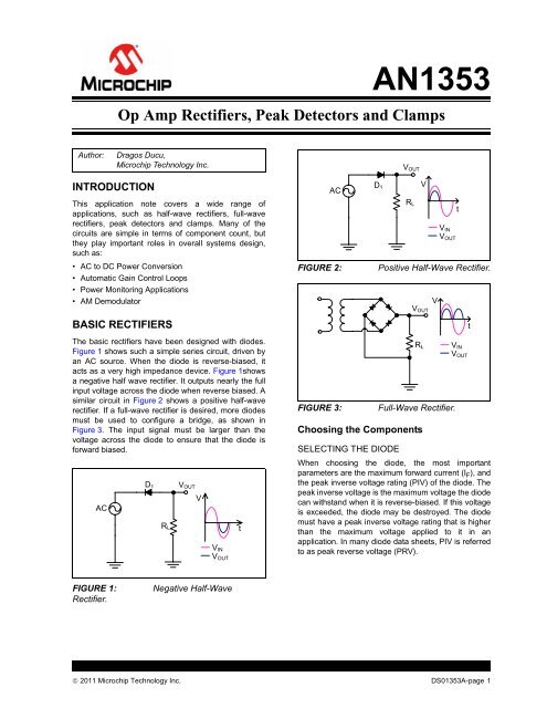
AN1353 Op Amp Rectifiers, Peak Detectors and Clamps - EEWeb
AN1353 Op Amp Rectifiers, Peak Detectors and Clamps - EEWeb
AN1353 Op Amp Rectifiers, Peak Detectors and Clamps - EEWeb

You also want an ePaper? Increase the reach of your titles
YUMPU automatically turns print PDFs into web optimized ePapers that Google loves.
Author: Dragos Ducu,<br />
Microchip Technology Inc.<br />
INTRODUCTION<br />
This application note covers a wide range of<br />
applications, such as half-wave rectifiers, full-wave<br />
rectifiers, peak detectors <strong>and</strong> clamps. Many of the<br />
circuits are simple in terms of component count, but<br />
they play important roles in overall systems design,<br />
such as:<br />
• AC to DC Power Conversion<br />
• Automatic Gain Control Loops<br />
• Power Monitoring Applications<br />
• AM Demodulator<br />
BASIC RECTIFIERS<br />
The basic rectifiers have been designed with diodes.<br />
Figure 1 shows such a simple series circuit, driven by<br />
an AC source. When the diode is reverse-biased, it<br />
acts as a very high impedance device. Figure 1shows<br />
a negative half wave rectifier. It outputs nearly the full<br />
input voltage across the diode when reverse biased. A<br />
similar circuit in Figure 2 shows a positive half-wave<br />
rectifier. If a full-wave rectifier is desired, more diodes<br />
must be used to configure a bridge, as shown in<br />
Figure 3. The input signal must be larger than the<br />
voltage across the diode to ensure that the diode is<br />
forward biased.<br />
AC<br />
FIGURE 1: Negative Half-Wave<br />
Rectifier.<br />
<strong>AN1353</strong><br />
<strong>Op</strong> <strong>Amp</strong> <strong>Rectifiers</strong>, <strong>Peak</strong> <strong>Detectors</strong> <strong>and</strong> <strong>Clamps</strong><br />
D1<br />
RL<br />
VOUT<br />
V<br />
VIN<br />
VOUT<br />
t<br />
FIGURE 2: Positive Half-Wave Rectifier.<br />
FIGURE 3: Full-Wave Rectifier.<br />
Choosing the Components<br />
SELECTING THE DIODE<br />
When choosing the diode, the most important<br />
parameters are the maximum forward current (I F), <strong>and</strong><br />
the peak inverse voltage rating (PIV) of the diode. The<br />
peak inverse voltage is the maximum voltage the diode<br />
can withst<strong>and</strong> when it is reverse-biased. If this voltage<br />
is exceeded, the diode may be destroyed. The diode<br />
must have a peak inverse voltage rating that is higher<br />
than the maximum voltage applied to it in an<br />
application. In many diode data sheets, PIV is referred<br />
to as peak reverse voltage (PRV).<br />
© 2011 Microchip Technology Inc. DS01353A-page 1<br />
AC<br />
D1<br />
VOUT<br />
RL<br />
V<br />
VOUT<br />
RL<br />
V<br />
VIN<br />
VOUT<br />
t<br />
VIN<br />
VOUT<br />
t
<strong>AN1353</strong><br />
The peak inverse voltage of the diode will be equal to:<br />
EQUATION 1:<br />
Where:<br />
VPIV( rating)<br />
≥ VPK( max)<br />
+ VDon ( )<br />
VPIV = <strong>Peak</strong> inverse voltage<br />
VPK(max) = Maximum peak amplitude<br />
VD(on) = Diode voltage on when in<br />
Every diode has a parasitic capacitance <strong>and</strong>, by<br />
default, has a time charge storage. This charge storage<br />
mechanism is nonlinear, leading to a nonlinear<br />
capacitance. This effect is very important because the<br />
nonlinearity of the diode can generate harmonics. For<br />
example, the output voltage becomes negative for a<br />
short time. This period is called reverse recovery time.<br />
During the transition, the diode’s parasitic capacitance<br />
will interact with the circuit resistors to modify the<br />
circuit’s behavior.<br />
For most general purpose applications, low power<br />
signal diodes such as 1N4148, are adequate. For high<br />
accuracy applications, where offset errors <strong>and</strong> reverse<br />
diode leakage current are critical, a low leakage FET<br />
transistor can be used as a diode (short Drain <strong>and</strong><br />
Source together), such as 2N4117A. In applications<br />
where speed is important, silicon Schottky barrier<br />
diodes are worth considering, since they have a low<br />
forward ON voltage of only 0.4V <strong>and</strong> are fast.<br />
SELECTING THE RESISTOR<br />
The resistor is selected based on the load current.<br />
One limitation is the value of load resistor. The value of<br />
the load resistor must be less than the diode resistance<br />
when in reverse bias. The parasitic capacitance of the<br />
diode interacts with the load resistor causing a time<br />
constant. If this constant is large, the output voltage will<br />
have a delayed recovery.<br />
Advantages <strong>and</strong> Disadvantages<br />
The major disadvantage of these circuits is the<br />
nonlinearity of the diodes. If the input signal is smaller<br />
than the threshold voltage of the diode, the signal<br />
cannot be recovered. To reduce the threshold voltage<br />
of the diode <strong>and</strong> improve linearity, we need to include<br />
the diode into the feedback loop of the operational<br />
amplifier.<br />
Practical Examples<br />
Figures 4 – 6 show practical samples when using the<br />
1N4001 diode <strong>and</strong> R L =1 kΩ. The frequency is<br />
f=1kHz.<br />
TABLE 1: ADVANTAGES AND<br />
DISADVANTAGES OF THE<br />
CIRCUIT<br />
Advantages Disadvantages<br />
- Uses few compo- - Poor accuracy<br />
nents<br />
- Simple design - The rectified voltage depends<br />
on the diode voltage threshold<br />
FIGURE 4: Negative Half-Wave<br />
Rectifier Sample.<br />
FIGURE 5: Positive Half-Wave Rectifier<br />
Sample.<br />
FIGURE 6: Full-Wave Rectifier Sample.<br />
DS01353A-page 2 © 2011 Microchip Technology Inc.<br />
Magnitude (V)<br />
Magnitude (V)<br />
Magnitude(V)<br />
1.5<br />
1<br />
0.5<br />
0<br />
-0.5<br />
-1<br />
-1.5<br />
1.5<br />
1<br />
0.5<br />
0<br />
-0.5<br />
-1<br />
-1.5<br />
1.5<br />
1<br />
0.5<br />
0<br />
-0.5<br />
-1<br />
-1.5<br />
Time (1 ms/div)<br />
Time (1 ms/div)<br />
Time (1 ms/div)<br />
V OUT<br />
V IN<br />
V OUT<br />
V IN<br />
VOUT VIN
ACTIVE HALF-WAVE RECTIFIER<br />
The simplest op amp half-wave rectifier is shown in<br />
Figure 7. When the V IN is positive, the diode is forward<br />
biased; the signal can be found on the R L load. When<br />
the V IN is negative, the diode is non-conductive, <strong>and</strong><br />
the output signal is ground (0V).<br />
FIGURE 7: <strong>Op</strong> <strong>Amp</strong> Half-Wave Rectifier.<br />
The big advantage of this circuit is represented by the<br />
small threshold voltage <strong>and</strong> linearity. This is more<br />
convenient than the basic rectifiers, since this circuit is<br />
able to rectify signals smaller than the diode threshold<br />
voltage.<br />
Magnitude (V)<br />
VOUT<br />
FIGURE 8: Circuit Behavior on<br />
Low Frequency.<br />
This circuit has limitations. The rectifier’s speed is<br />
limited by the op amp b<strong>and</strong>width. This effect is<br />
illustrated in Figure 9, where the rectified output signal<br />
overlaps the input signal. The maximum frequency<br />
that can be rectified is determined by the slew rate of<br />
the op amp.<br />
Magnitude (V)<br />
1.50<br />
1.00<br />
0.50<br />
0.00<br />
-0.50<br />
-1.00<br />
-1.50<br />
1.5<br />
1<br />
0.5<br />
0<br />
-0.5<br />
-1<br />
-1.5<br />
VIN<br />
-<br />
+<br />
AO1<br />
D1<br />
Time (1 ms/div)<br />
Time (50 µs/div)<br />
RL<br />
FIGURE 9: Output Limitation on<br />
High-Frequency Input Signals.<br />
V OUT<br />
V IN<br />
V OUT<br />
V IN<br />
Choosing the Components<br />
<strong>AN1353</strong><br />
SELECTING THE OP AMP<br />
When selecting the op amp, two important<br />
characteristics must be considered:<br />
• Gain B<strong>and</strong>width Product<br />
• Slew Rate (SR)<br />
The minimum gain b<strong>and</strong>width product requirement can<br />
be estimated in Equation 2.<br />
EQUATION 2:<br />
Where:<br />
The next parameter that needs to be considered is the<br />
slew rate (SR). This is the maximum time rate change<br />
at the output of the op amp; it shows how fast the output<br />
can follow the input signal. The SR parameter can be<br />
found in the selected op amp’s data sheet.<br />
The full b<strong>and</strong>width product (FPBW) defines the highest<br />
frequency sine wave that will not be distorted by the<br />
slew rate limit.<br />
EQUATION 3:<br />
f GBWP<br />
10 × G × f<br />
INPUT<br />
SELECTING THE DIODE AND THE RESISTOR<br />
Refer to the sections Selecting the Diode <strong>and</strong> Selecting<br />
The Resistor, in the Basic <strong>Rectifiers</strong> section, for details<br />
on choosing the appropriate components.<br />
Advantages <strong>and</strong> Disadvantages<br />
Table 2 shows the main advantages <strong>and</strong><br />
disadvantages of a half-wave rectifier.<br />
TABLE 2: ADVANTAGES AND<br />
DISADVANTAGES OF THE<br />
CIRCUIT<br />
Advantages Disadvantages<br />
- Uses few components - Load dependant<br />
- Good linearity - Limited op amp b<strong>and</strong>width<br />
© 2011 Microchip Technology Inc. DS01353A-page 3<br />
=<br />
fGBWP = Gain b<strong>and</strong>width product<br />
G = DC gain<br />
fINPUT = Maximum input frequency<br />
SR=<br />
ΔVOUT -----------------<br />
ΔT max<br />
SR<br />
FPBW=<br />
-----------------------------------π<br />
× VOUT( p – p)
<strong>AN1353</strong><br />
Practical Example<br />
This example of a half-wave rectifier uses an<br />
MBRM110LT3 Schottky diode <strong>and</strong> the MCP661 op<br />
amp with different load resistors. For this example, the<br />
value of the load resistor is less than 1 kΩ, to avoid<br />
glitches in the negative cycle. The Schottky diode is<br />
chosen for higher speed than a small signal silicon<br />
diode. Figures 10 <strong>and</strong> 11 below are examples of a<br />
1 kHz input signal <strong>and</strong> different load resistors. Note that<br />
for the small values of the resistor (i.e. 100Ω), the glitch<br />
is smaller.<br />
Magnitude (V)<br />
FIGURE 10: Half-Wave Rectifier with<br />
R L =100Ω.<br />
Magnitude (V)<br />
0.2<br />
0.15<br />
0.1<br />
0.05<br />
0<br />
-0.05<br />
-0.1<br />
-0.15<br />
-0.2<br />
0.2<br />
0.15<br />
0.1<br />
0.05<br />
0<br />
-0.05<br />
-0.1<br />
-0.15<br />
-0.2<br />
R L = 100 Ohm<br />
Time (500 µs/div)<br />
R L = 1 k<br />
Time (500 µs/div)<br />
V OUT<br />
V IN<br />
V OUT<br />
V IN<br />
FIGURE 11: Half-Wave Rectifier with<br />
R L =1kΩ.<br />
Improved <strong>Op</strong> <strong>Amp</strong> Half-Wave Rectifier<br />
Figure 12 shows a half-wave rectifier circuit with<br />
improved performance. The additional diode prevents<br />
the op amp's output from swinging to the negative<br />
supply rail. The low level linearity is also improved.<br />
Although the op amp still operates in open-loop at the<br />
point where the input swings from positive to negative<br />
or vice versa, the range is limited by the diode <strong>and</strong> the<br />
load resistor.<br />
When the input signal is positive, D1 is open <strong>and</strong> D2 conducts. The output signal is zero because one side<br />
of R2 is connected to the virtual ground, with no current<br />
through it. When the input is negative, D1 conducts <strong>and</strong><br />
D2 is open. The output follows the positive input cycle<br />
with a gain of G = -R2 /R1 .<br />
VIN R1<br />
FIGURE 12: Have-Wave Rectifier Circuit<br />
Improvement.<br />
This type of circuit also has limitations. The input<br />
impedance is determined by the input resistor. It must<br />
be driven from a low-impedance source. Likewise, the<br />
input resistor R 3 shown in Figure 12 is also optional,<br />
<strong>and</strong> is needed only if there is no DC path to ground.<br />
Choosing the Components<br />
Refer to the section Selecting the <strong>Op</strong> <strong>Amp</strong> in the Active<br />
Half-Wave Rectifier section, <strong>and</strong> to the section<br />
Selecting the Diode in the section Basic <strong>Rectifiers</strong>, for<br />
details on choosing the appropriate components.<br />
SELECTING THE RESISTORS<br />
The DC gain is determined in Equation 4:<br />
EQUATION 4:<br />
DS01353A-page 4 © 2011 Microchip Technology Inc.<br />
R3<br />
R2<br />
D2<br />
-<br />
+<br />
AO1<br />
R<br />
2<br />
G = –<br />
------<br />
R<br />
1<br />
D1<br />
where G = DC gain<br />
RL<br />
VOUT
Resistors R1 <strong>and</strong> R2 are selected based on the<br />
application design:<br />
• For a general purpose application, the resistor’s<br />
value should be between 1 kΩ <strong>and</strong> 100 kΩ.<br />
• For a high speed application, the resistor’s value<br />
should be between 100 Ω <strong>and</strong> 1 kΩ (consume<br />
more power)<br />
• For portable applications between 1 MΩ <strong>and</strong><br />
10 MΩ.<br />
The R3 is added to minimize the error caused by the<br />
input bias current.<br />
EQUATION 5:<br />
Advantages <strong>and</strong> Disadvantages<br />
Table 3 shows the main advantages <strong>and</strong><br />
disadvantages of an improved half-wave rectifier.<br />
TABLE 3: ADVANTAGES AND<br />
DISADVANTAGES OF THE<br />
CIRCUIT<br />
Advantages Disadvantages<br />
- Good linearity - Uses more components<br />
- The second diode<br />
prevents the op amp from<br />
swinging into the negative<br />
cycle<br />
Practical Example<br />
The example in Figure 13 is based on the circuit in<br />
Figure 12, <strong>and</strong> uses the MCP661 op amp, two<br />
MBRM110LT3 Schottky diodes, R L =1kΩ, R 2 =10 kΩ<br />
<strong>and</strong> R 1 =1kΩ. The input frequency is 1 kHz.<br />
Magnitude (V)<br />
0.2<br />
0.15<br />
0.1<br />
0.05<br />
0<br />
-0.05<br />
-0.1<br />
-0.15<br />
-0.2<br />
R × R<br />
1 2<br />
R<br />
3<br />
= --------------------<br />
R<br />
1<br />
+ R<br />
2<br />
- Low impedance<br />
because of R 1<br />
R L = 1 k<br />
Time (1 ms/div)<br />
V OUT<br />
V IN<br />
FIGURE 13: Improved Half-Wave<br />
Rectifier with R L =1KΩ.<br />
<strong>AN1353</strong><br />
For an input frequency under 600 kHz, the circuit<br />
performs properly. For frequencies larger than this<br />
value, the output signal is distorted.<br />
FIGURE 14: Circuit Behavior with<br />
600 kHz Input Frequency.<br />
To design a negative half-wave rectifier using the same<br />
components, we only have to invert the diodes, as<br />
shown in the circuit in Figure 15.<br />
FIGURE 15: Negative Half-Wave<br />
Rectifier.<br />
FIGURE 16: Negative Cycle Rectifier<br />
Sample.<br />
© 2011 Microchip Technology Inc. DS01353A-page 5<br />
Magnitude (V)<br />
Magnitude (V)<br />
1<br />
0.8<br />
0.6<br />
0.4<br />
0.2<br />
0<br />
-0.2<br />
-0.4<br />
-0.6<br />
-0.8<br />
-1<br />
VIN R1<br />
0.2<br />
0.15<br />
0.1<br />
0.05<br />
0<br />
-0.05<br />
-0.1<br />
-0.15<br />
-0.2<br />
R3<br />
Time (0.2 µs/div)<br />
R2<br />
D2<br />
-<br />
+<br />
AO1<br />
D1<br />
Time (1 ms/div)<br />
RL<br />
V OUT<br />
V IN<br />
VOUT<br />
V OUT<br />
V IN
<strong>AN1353</strong><br />
ACTIVE FULL-WAVE RECTIFIER<br />
Full-wave rectifiers are more complex, compared to the<br />
half-wave circuits. Full-wave rectifiers output one<br />
polarity of the input signal <strong>and</strong> invert the other. A circuit<br />
for a full-wave rectifier is illustrated in Figure 17.<br />
VIN<br />
FIGURE 17: Full-Wave Rectifier Circuit.<br />
When in the negative cycle of the input signal, diode D 1<br />
is forward biased, <strong>and</strong> the output voltage follows the<br />
input. When the input signal (V IN ) is positive, D 1 is nonconductive<br />
<strong>and</strong> the input signal passes through the<br />
feedback resistor (R 2 ), which forms a voltage divider<br />
with R 1 <strong>and</strong> R L . Equation 6 shows the calculation for<br />
the output voltage:<br />
EQUATION 6:<br />
Where:<br />
R1<br />
R3<br />
-<br />
+<br />
V+<br />
When -GM = GP, the full-wave output is symmetric.<br />
Note that the output is not buffered, so it should be<br />
connected only to a circuit with high impedance, much<br />
higher than R L .<br />
Choosing the Components<br />
VOUT<br />
Refer to the section Selecting the Diode in the section<br />
Basic <strong>Rectifiers</strong>, <strong>and</strong> to the section Selecting the <strong>Op</strong><br />
<strong>Amp</strong> in the section Active Half-Wave Rectifier, for<br />
details on choosing the appropriate components.<br />
R2<br />
AO1<br />
D1<br />
RL<br />
V<br />
OUT<br />
= V<br />
IN<br />
× GM;<br />
V<br />
IN<br />
< 0<br />
V<br />
OUT<br />
= V<br />
IN<br />
× GP ; V<br />
IN<br />
> 0<br />
GM<br />
–<br />
= --------<br />
R2 R1 R<br />
L<br />
GP = ----------------------------------<br />
R<br />
1<br />
+ R<br />
2<br />
+ R<br />
L<br />
SELECTING THE RESISTORS<br />
When selecting the resistors for the circuit in Figure 17,<br />
-GM must be equal to GP. The result is shown in<br />
Equation 7:<br />
EQUATION 7:<br />
R2 × ( R1 + R2 + R<br />
L<br />
) =<br />
R1 × R<br />
L<br />
R 3 is added to minimize the error caused by the input<br />
bias current. Refer to the section Selecting the<br />
Resistors, in the section Improved <strong>Op</strong> <strong>Amp</strong> Half-Wave<br />
Rectifier, for details on the selection of the resistor.<br />
Advantages <strong>and</strong> Disadvantages<br />
TABLE 4: ADVANTAGES AND<br />
DISADVANTAGES OF THE<br />
CIRCUIT<br />
Advantages Disadvantages<br />
- Uses only one op amp - Low input resistance<br />
- Uses a small number<br />
of external components<br />
Practical Example<br />
- The source <strong>and</strong> load<br />
resistance affect rectifying<br />
- Uses a single supply - A reactive load (capacitor<br />
or coil) cannot be tolerated<br />
without a buffer<br />
- Has a low impedance<br />
because of R1 This design uses an MCP661 <strong>and</strong> a general purpose<br />
diode rectifier 1N4148. The input frequency is 1 kHz.<br />
Table 5 shows the resistor values recommended to<br />
obtain the same amplitude with each input cycle:<br />
TABLE 5: VALUES FOR RECTIFIED,<br />
EQUAL AMPLITUDE<br />
Resistor Value (kΩ)<br />
The values of the resistors can be scaled depending on<br />
the application: high speed, portable or general<br />
purpose. For more details, refer to the section<br />
Selecting the Resistors, in the section Improved <strong>Op</strong><br />
<strong>Amp</strong> Half-Wave Rectifier. Figure 18 shows the result of<br />
the full-wave rectifier circuit simulation.<br />
DS01353A-page 6 © 2011 Microchip Technology Inc.<br />
R1 R2 RL 2<br />
1<br />
3
Magnitude (V)<br />
0.2<br />
0.15<br />
0.1<br />
0.05<br />
0<br />
-0.05<br />
-0.1<br />
-0.15<br />
-0.2<br />
V OUT<br />
V IN<br />
Time (1ms/div)<br />
FIGURE 18: Full-Wave Rectifier Circuit<br />
Simulation with the Recommended Values of the<br />
Resistors.<br />
TWO STAGE OP AMP FULL-WAVE<br />
RECTIFIER<br />
Another full-wave rectifier can be obtained by including<br />
an adder to the single-wave rectifier, which subtracts<br />
V IN from the rectified signal. The rectifier stage consists<br />
of A O1, R 1, R 2, D 1 <strong>and</strong> D 2, while the adder stage<br />
consists of A O2 , R 3 , R 4 <strong>and</strong> R 5 .<br />
D2<br />
R2<br />
VIN R1<br />
- D1<br />
R3<br />
+<br />
AO1<br />
VO1<br />
FIGURE 19: Two Stage <strong>Op</strong> <strong>Amp</strong> Full-<br />
Wave Rectifier Circuit.<br />
VOUT<br />
When VIN is positive, D1 is forward-biased <strong>and</strong> D2 is<br />
reverse-biased, while when VIN is negative, D2 is<br />
forward-biased <strong>and</strong> D1 is reversed-biased. The second<br />
stage adds VIN <strong>and</strong> VO1 <strong>and</strong> inverts the polarity of the<br />
resulting signal. The output voltage for the positive<br />
cycle of the input voltage is calculated in Equation 8.<br />
For the negative cycle of the input voltage (VIN ), D1 blocks the signal, while D2 conducts the whole current<br />
coming from the input. In this case, the output voltage<br />
for the first stage is VO1 =0V.<br />
For the positive cycle of the input signal, VO1 is<br />
negative <strong>and</strong>, in this case, the adder stage combines<br />
the input signals with equal amplitudes, one positive<br />
<strong>and</strong> one negative.<br />
R4<br />
R6<br />
-<br />
+<br />
R5<br />
AO2<br />
EQUATION 8:<br />
Where:<br />
Equation 9 calculates the output voltage:<br />
Choosing the Components<br />
<strong>AN1353</strong><br />
To obtain a good performance for the two stage circuit,<br />
the tolerance of resistors R1 to R5 should be 1%, or<br />
better; this makes the gains (for negative <strong>and</strong> positive<br />
VIN ) match well. The circuit in Figure 19 has a good<br />
linearity, down to a couple of mV at low frequencies, but<br />
the high-frequency response is limited by the op amp<br />
b<strong>and</strong>width.<br />
Refer to the section Selecting the Diode in the section<br />
Basic <strong>Rectifiers</strong>, <strong>and</strong> to the section Selecting the <strong>Op</strong><br />
<strong>Amp</strong> in the section Active Half-Wave Rectifier, for<br />
details on choosing the appropriate components.<br />
SELECTING THE RESISTORS<br />
R1 <strong>and</strong> R2 give the gain for the first stage; R3 <strong>and</strong> R5 for the second stage.<br />
To get the same amplitude for both cycles, choose<br />
R1 =R3 =R4 <strong>and</strong> R2 =R5 =2xR1. EQUATION 10:<br />
R6 is added to minimize the error caused by the input<br />
bias current. Refer to the section Selecting the<br />
Resistors, in the section Improved <strong>Op</strong> <strong>Amp</strong> Half-Wave<br />
Rectifier, for details on choosing the appropriate<br />
components.<br />
If a greater sensitivity <strong>and</strong> high frequency is desired, it<br />
is recommended to use lower resistance value, high<br />
speed diodes <strong>and</strong> faster op amps.<br />
© 2011 Microchip Technology Inc. DS01353A-page 7<br />
V O1<br />
G<br />
V O1<br />
=<br />
V<br />
IN<br />
× G, when V<br />
IN<br />
> 0<br />
–<br />
= --------<br />
=<br />
R1 R2 0, when V < 0<br />
IN<br />
EQUATION 9:<br />
R<br />
5<br />
× V R<br />
O1 5<br />
× V<br />
IN<br />
V = – ----------------------- – ----------------------<br />
OUT R R<br />
3 4<br />
R × ( V + V )<br />
5 O1 IN<br />
V =<br />
–<br />
OUT<br />
----------------------------------------------<br />
R<br />
1
<strong>AN1353</strong><br />
Advantages <strong>and</strong> Disadvantages<br />
Table 6 shows the advantages <strong>and</strong> disadvantages of a<br />
two stage op amp full-wave rectifier.<br />
TABLE 6: ADVANTAGES AND<br />
DISADVANTAGES OF THE<br />
CIRCUIT<br />
Advantages Disadvantages<br />
- Very good performance - Uses two op amps<br />
- Low output impedance - Low input resistance<br />
- Multiple passive<br />
components<br />
Practical Example<br />
This example uses the MCP6021 device, two 1N4148<br />
diodes, R1 =1kΩ, R2 =2kΩ, R3 =1kΩ, R4 =1kΩ,<br />
<strong>and</strong> R5 =2kΩ. The input signal frequency is f = 1 kHz.<br />
Figure 20 shows the result of the simulation for the fullwave<br />
rectifier shown in Figure 19:<br />
Magnitude (V)<br />
1<br />
0.8<br />
0.6<br />
0.4<br />
0.2<br />
0<br />
-0.2<br />
-0.4<br />
-0.6<br />
-0.8<br />
-1<br />
V OUT<br />
V IN<br />
Time (1 ms/div)<br />
FIGURE 20: Full-Wave Rectifier Circuit<br />
Simulation.<br />
For more topologies of the full-wave rectifier, refer to<br />
the Appendix section.<br />
Figure 21 shows the behavior of the circuit at the<br />
maximum frequency tolerated.<br />
Magnitude (V)<br />
1<br />
0.8<br />
0.6<br />
0.4<br />
0.2<br />
0<br />
-0.2<br />
-0.4<br />
-0.6<br />
-0.8<br />
-1<br />
Time (10 µs/div)<br />
V OUT<br />
V IN<br />
FIGURE 21: Circuit Behavior when Input<br />
Frequency = 100 kHz.<br />
BASIC PEAK DETECTORS<br />
The purpose of this circuit is to detect the maximum<br />
magnitude of a signal over a period of time. The<br />
operation of a peak detector can be illustrated using a<br />
simple diode <strong>and</strong> capacitor, as shown in Figure 22.<br />
FIGURE 22: Basic <strong>Peak</strong> Detector<br />
<strong>Op</strong>eration.<br />
Choosing the Components<br />
When choosing the resistor, the limits must be<br />
considered: rdf τ 2 >> 1/f c , where f m is the modulation<br />
frequency <strong>and</strong> f c is the carrier frequency.<br />
DS01353A-page 8 © 2011 Microchip Technology Inc.<br />
VIN<br />
D1<br />
C1<br />
V<br />
PEAK<br />
ΔV=<br />
------------------f<br />
× τ<br />
2<br />
VOUT<br />
R1<br />
VPEAK = <strong>Amp</strong>litude maximum value<br />
f = Input signal frequency<br />
τ2 = Discharge time constant<br />
EQUATION 12:<br />
t<br />
V<br />
DROP<br />
= V<br />
PEAK<br />
× exp⎛–<br />
----- ⎞<br />
⎝ τ ⎠<br />
2<br />
Where: τ2 = time constant
Advantages <strong>and</strong> Disadvantages<br />
Table 7 identifies some of the advantages <strong>and</strong><br />
disadvantages of the peak detectors.<br />
TABLE 7: ADVANTAGES AND<br />
DISADVANTAGES OF THE<br />
CIRCUIT<br />
Advantages Disadvantages<br />
- Uses few<br />
components<br />
Practical Example<br />
- The output voltage is one<br />
diode drop below the actual output<br />
- Very low cost - The input impedance is<br />
variable due to the input<br />
characteristics of the diode<br />
- The discharge is very slow due<br />
to the leakage current<br />
The simulation in Figure 23 shows that this circuit does<br />
not reach the peak amplitude of the input signal, but is<br />
good for quickly following sudden changes in the<br />
signal's amplitude. However, it has significant ripple.<br />
This example uses a 1N4148 diode, C 1 =1µF,<br />
R 1 =100kΩ <strong>and</strong> f = 1 kHz.<br />
Magnitude(V)<br />
18<br />
16<br />
14<br />
12<br />
10<br />
8<br />
6<br />
4<br />
2<br />
0<br />
Time (20 ms/div)<br />
FIGURE 23: <strong>Peak</strong> Detector Simulation.<br />
Two-Stage Active <strong>Peak</strong> Detector<br />
In many applications, the voltage drop is not desired.<br />
To avoid this, we need to include a diode into the loop<br />
of the op amp, as shown in Figure 24.<br />
A two-stage peak detector is shown in Figure 24. In this<br />
circuit, AO1 , R1 , R2 , D1 , R5 <strong>and</strong> C1 represent the first<br />
stage, while AO2 , R3 <strong>and</strong> R4 is the second stage. AO1 charges the capacitor up to the peak value, <strong>and</strong> AO2 acts as an output buffer. AO1 removes the variability of<br />
the input impedance, while AO2 removes the variability<br />
of the output impedance.<br />
V OUT<br />
V IN<br />
<strong>AN1353</strong><br />
FIGURE 24: Two-Stage <strong>Peak</strong> Detector<br />
Circuit.<br />
The time constant for charging C1 is very short, <strong>and</strong><br />
primarily consists of the C1 <strong>and</strong> the forward resistance<br />
of the diode. Thus, C1 charges almost instantly to the<br />
peak output of the input signal (VIN ). When VIN goes<br />
below the output signal (VOUT ), diode D1 becomes<br />
reverse-biased. The only discharge path for C1 is<br />
through R5 , via leakage or op amp bias currents. The<br />
discharge time constant is much longer than the charge<br />
time constant, so C1 holds its charge <strong>and</strong> presents a<br />
steady input voltage to AO2 that is equal to the peak<br />
amplitude of the input signal. AO2 is a buffer amplifier<br />
that prevents unintentional discharging of the C1 ,<br />
caused by the loading impedance of the following<br />
circuit. If the R5C1 time constant is too short, then the<br />
voltage on C1 will not be constant, <strong>and</strong> will have a high<br />
value of ripple. On the other h<strong>and</strong>, if the R5C1 time<br />
constant is too long, the circuit cannot respond quickly<br />
to the changes in the input amplitude.<br />
The lower frequency limit is the frequency that causes<br />
the ripple voltage to exceed the maximum allowable<br />
level. It can be estimated by applying the basic<br />
discharge equation for capacitors (Equation 13):<br />
The response time describes how quickly C 1 can<br />
respond to the decreases in the magnitude of the input<br />
signal. This can be computed from the basic discharge<br />
equation. However, if we assume that the capacitor is<br />
charged to peak <strong>and</strong> discharges towards an eventual<br />
value of 0, we can use the simplified form<br />
(Equation 14).<br />
© 2011 Microchip Technology Inc. DS01353A-page 9<br />
VIN<br />
R1<br />
-<br />
+<br />
AO1<br />
R2<br />
D1<br />
R5<br />
R3<br />
C1<br />
-<br />
R4<br />
+<br />
AO2<br />
EQUATION 13:<br />
f<br />
O<br />
=<br />
1<br />
---------------------------------------------------------<br />
V – V<br />
o<br />
R × C × ln ---------------<br />
5 1 V– V<br />
c<br />
Where:<br />
VOUT<br />
V = Capacitor’s discharge voltage<br />
VC = Minimum allowable voltage on the<br />
capacitor<br />
VO = Initial charge of the capacitor
<strong>AN1353</strong><br />
EQUATION 14:<br />
Where:<br />
V<br />
PK( old)<br />
t = R × C × ln-------------------------- R 5 1 V<br />
PK( new)<br />
VPK(old) = <strong>Peak</strong> input signal amplitude<br />
before the decrease<br />
VPK(new) = <strong>Peak</strong> input signal amplitude after<br />
the decrease<br />
Choosing the Components<br />
Refer to the section Selecting the Diode in the section<br />
Basic <strong>Rectifiers</strong>, <strong>and</strong> to the section Selecting the <strong>Op</strong><br />
<strong>Amp</strong>, in the section Active Half-Wave Rectifier, for<br />
details on choosing the appropriate components.<br />
SELECTING THE RESISTORS<br />
R3 limits the current into the positive input of the AO2 when power is disconnected from the circuit. Without<br />
this resistor, the AO2 may be damaged as C1 discharges through it. For capacitors smaller than 1 µF,<br />
resistor R3 can normally be omitted. Resistor R4 minimizes the effects of the bias currents in AO2 .<br />
Resistor R2 limits the current into the negative input of<br />
AO1 when power is removed from the circuit.<br />
There are two conflicting circuit parameters that affect<br />
the choice of the values for R5 <strong>and</strong> C1 : allowable ripple<br />
voltage across C1 <strong>and</strong> response time. In general, a<br />
faster response time leads to greater ripple.<br />
Refer to the section Selecting the Resistors, in the<br />
section Improved <strong>Op</strong> <strong>Amp</strong> Half-Wave Rectifier, for<br />
details on choosing the appropriate components.<br />
Practical Example<br />
Figure 25 illustrates the simulation result for one peak<br />
detector, realized with MCP661 device, diode 1N4148,<br />
R 5 =100kΩ <strong>and</strong> C 1 = 1 µF. Input signal has the<br />
frequency equal to 1 kHz.<br />
Magnitude (V)<br />
0.2<br />
0.19<br />
0.18<br />
0.17<br />
0.16<br />
0.15<br />
0.14<br />
0.13<br />
0.12<br />
0.11<br />
0.1<br />
Time (1 ms/div)<br />
FIGURE 25: One <strong>Peak</strong> Detector<br />
Simulation Results.<br />
V OUT<br />
V IN<br />
For more topologies on the peak detectors, refer to the<br />
Appendix.<br />
BASIC CLAMP<br />
A clamp is used to shift the DC reference level of the<br />
input signal. Figure 26 shows a basic diode clamp. Its<br />
purpose is to shift the average or the DC level of the<br />
input signal without altering the wave shape.<br />
When VOUT > VREF <strong>and</strong> the input signal is fast, D1 is off,<br />
C1 acts like a short circuit, <strong>and</strong> VOUT looks like the<br />
input. With slow signals, C1 acts like an open circuit <strong>and</strong><br />
VOUT will exponentially decay towards VREF. When VOUT < VREF, VOUT becomes VREF -VD(on), D1 turns on <strong>and</strong> C1 is forced to accept a new voltage that<br />
shifts the input to the desired minimum VOUT .<br />
For low-amplitude signals, the diode drop becomes<br />
significant. In fact, the circuit cannot be used at all if the<br />
peak input signal is below the diode threshold, since<br />
the diode cannot be forward-biased. An active clamp is<br />
needed for signals with an amplitude of millivolts.<br />
Figure 26 shows a negative clamp; it clamps the<br />
negative extreme of the signal to (near) VREF .<br />
Reversing the diode creates a positive clamp.<br />
FIGURE 26: Basic Diode Negative<br />
Clamp.<br />
Practical Example<br />
Figure 27 shows a simulation for the above schematic<br />
with V REF =2V, C 1 = 1 nF <strong>and</strong> diode 1N4148. The<br />
input signal has the frequency equal to 500 Hz.<br />
FIGURE 27: Basic Diode Clamp –<br />
Circuit Simulation.<br />
DS01353A-page 10 © 2011 Microchip Technology Inc.<br />
Magnitude (V)<br />
4<br />
3.5<br />
3<br />
2.5<br />
2<br />
1.5<br />
1<br />
0.5<br />
0<br />
-0.5<br />
-1<br />
AC<br />
V OUT<br />
V IN<br />
C1<br />
R1<br />
Time (10 ms/div)<br />
D1<br />
VOUT<br />
VREF
Active Clamp<br />
To reduce the threshold voltage of the diode, <strong>and</strong> for<br />
linearization, the circuit needs a diode in the feedback<br />
loop of the operational amplifier.<br />
Figure 28 shows an op amp clamp where the input<br />
signal is positive <strong>and</strong> D1 is forward-biased. The diode<br />
converts the circuit into a voltage follower with<br />
reference to the positive input. This means that the<br />
output of the op amp has approximately the same<br />
voltage as the reference voltage. When the input signal<br />
is negative, the diode is reversed-biased. The op amp<br />
will also be at the reference voltage level. Capacitor C1 is charged with the difference of potential between VIN <strong>and</strong> VREF. This effectively disconnects the op amp from<br />
the circuit so the output will be the same as VIN plus<br />
C1 ’s voltage. The capacitor has no rapid discharge path<br />
<strong>and</strong> will act as a DC source, providing the clamping<br />
action.<br />
VIN<br />
C1<br />
R1<br />
VREF<br />
-<br />
+<br />
AO1<br />
FIGURE 28: <strong>Op</strong> <strong>Amp</strong> Clamp.<br />
Choosing the Components<br />
VOUT<br />
Refer to the section Selecting the Diode, in the section<br />
Basic <strong>Rectifiers</strong>, <strong>and</strong> to the section Selecting the <strong>Op</strong><br />
<strong>Amp</strong>, in the section Active Half-Wave Rectifier, for<br />
details on choosing the appropriate components.<br />
SELECTING THE RESISTANCE AND THE<br />
CAPACITOR<br />
The input impedance of the circuit varies with the input<br />
frequency <strong>and</strong> with the state of the circuit. As frequency<br />
increases, the reactance of C1 decreases <strong>and</strong> lowers<br />
the input impedance.<br />
Usually, R1 gives the input impedance, so the chosen<br />
resistance should be the minimum of the desired<br />
impedance.<br />
The value of C1 is shown in Equation 15:<br />
D1<br />
+<br />
-<br />
AO2<br />
EQUATION 15:<br />
Where:<br />
Where:<br />
<strong>AN1353</strong><br />
R (-) <strong>and</strong> R (+) are calculated as a ratio between the<br />
maximum voltage allowed by the circuit on the input<br />
terminal <strong>and</strong> the maximum input bias current.<br />
Advantages <strong>and</strong> Disadvantages<br />
Table 8 shows the main advantages <strong>and</strong><br />
disadvantages of the clamp circuit.<br />
TABLE 8: ADVANTAGES AND<br />
DISADVANTAGES OF THE<br />
CIRCUIT<br />
Advantages Disadvantages<br />
- Uses only one op amp - The input impedance varies<br />
with the input frequency<br />
- Few external<br />
components<br />
- Adjustable level for<br />
voltage reference<br />
Practical Example<br />
- The output impedance<br />
varies with the input<br />
frequency<br />
- Uses a potentiometer<br />
- Uses a positive <strong>and</strong><br />
a negative voltage<br />
reference<br />
This example uses the MCP6021 device, a 1N4148<br />
diode, C 1 = 150 nF, R 1 =1.2kΩ, R 2 =43kΩ,<br />
R 3 =47kΩ, V REF = 0.7V. The input frequency is<br />
10 kHz. Figure 29 shows the simulation result for this<br />
example.<br />
© 2011 Microchip Technology Inc. DS01353A-page 11<br />
C 1<br />
16.7<br />
= ------------------<br />
R × flow f low = minimum frequency desired<br />
R = r dr || R (-) || R (+)<br />
rdr = Reversed diode resistance<br />
R (-) = Input resistance on the negative<br />
terminal of AO1 R (+) = Input resistance on the positive terminal<br />
of AO1 for voltage follower
<strong>AN1353</strong><br />
Magnitude (V)<br />
4<br />
3.5<br />
3<br />
2.5<br />
2<br />
1.5<br />
1<br />
0.5<br />
0<br />
-0.5<br />
-1<br />
FIGURE 29: <strong>Op</strong> <strong>Amp</strong> Clamp Circuit<br />
Simulation Result.<br />
CONCLUSION<br />
Time (100 ms/div)<br />
V OUT<br />
V IN<br />
This application note examined the circuits that can<br />
rectify the amplitude signal, detect the peak signal <strong>and</strong><br />
change the DC level of waveforms. The op amp-based<br />
solutions bring improvements to the basic solutions,<br />
such as operating with millivolt signals or isolating the<br />
output <strong>and</strong> input impedance. The applications<br />
proposed are based on low cost op amps, <strong>and</strong> offer<br />
circuits with few peripheral components, giving<br />
designers simple, but effective solutions to their<br />
problems.<br />
DS01353A-page 12 © 2011 Microchip Technology Inc.
APPENDIX<br />
This Appendix includes schematics for additional half<br />
<strong>and</strong> full-wave rectifiers, peak detectors <strong>and</strong> clamps.<br />
Each of these can be implemented using the rules<br />
presented in this application note.<br />
Half-Wave <strong>Rectifiers</strong><br />
Figures 30 –33 show more half-wave rectifiers with<br />
their DC transfer functions.<br />
FIGURE 30: Positive Half-Wave<br />
Rectifier 1.<br />
FIGURE 31: Negative Half-Wave<br />
Rectifier 1.<br />
VIN<br />
R1<br />
R1<br />
VIN<br />
VIN<br />
R1<br />
R2<br />
AO1<br />
-<br />
+<br />
R2<br />
AO1<br />
-<br />
+<br />
D2<br />
R2<br />
-<br />
+<br />
AO1<br />
D1<br />
D2<br />
D1<br />
D2<br />
D1<br />
VOUT<br />
VOUT<br />
VOUT<br />
FIGURE 32: Positive Half-Wave<br />
Rectifier 2.<br />
VOUT<br />
VOUT<br />
VIN<br />
VIN<br />
VOUT<br />
VIN<br />
<strong>AN1353</strong><br />
FIGURE 33: Negative Half-Wave<br />
Rectifier 2.<br />
Every one of these circuits can be used to design fullwave<br />
rectifiers by adding an op amp adder. This<br />
method is illustrated in Figure 19.<br />
Full-Wave <strong>Rectifiers</strong><br />
The circuits shown in this section are based on halfwave<br />
rectifiers. For example, the circuit in Figure 36<br />
contains two half-wave rectifiers, one for the positive<br />
cycle, the other for the negative cycle, <strong>and</strong> one<br />
difference (or adder) amplifier.<br />
For Figures 34 – 36, VOUT is positive. Reversing the<br />
diodes creates a negative rectifier.<br />
FIGURE 34: Two Stage Full-Wave<br />
Rectifier 1.<br />
FIGURE 35: Two Stage Full-Wave<br />
Rectifier 2.<br />
© 2011 Microchip Technology Inc. DS01353A-page 13<br />
VIN<br />
VIN<br />
R2<br />
D2<br />
R1<br />
-<br />
+<br />
AO1<br />
D1 VOUT<br />
VIN<br />
R1<br />
R1<br />
-<br />
+<br />
AO1<br />
R3<br />
R2<br />
AO1<br />
-<br />
+<br />
R4<br />
R2<br />
D1<br />
D1<br />
D2<br />
D2<br />
R3<br />
-<br />
+<br />
R4<br />
R4<br />
AO2<br />
R5<br />
-<br />
+<br />
VOUT<br />
VOUT<br />
AO2<br />
VIN<br />
VOUT
<strong>AN1353</strong><br />
VIN<br />
FIGURE 36: Three Stage Full-Wave<br />
Rectifier.<br />
<strong>Peak</strong> <strong>Detectors</strong><br />
The circuit in Figure 37 has the capacitor discharge<br />
through R 2, which causes the output to droop. Diode<br />
D 2 provides the local feedback around A O1 , once a<br />
peak has been detected. This prevents A O1 from<br />
saturating during the peak hold mode <strong>and</strong> decreases<br />
the peak acquisition time. You can omit D 2 , but the<br />
circuit will be slower when detecting peaks.<br />
VIN<br />
R1<br />
R1<br />
R1<br />
-<br />
+<br />
R3<br />
-<br />
+<br />
R3<br />
R2<br />
D2<br />
AO1<br />
R2<br />
D2<br />
AO2<br />
R2<br />
D1<br />
D1<br />
VOUT<br />
FIGURE 37: <strong>Peak</strong> Detector Rectifier 1.<br />
R5<br />
R4<br />
-<br />
R7<br />
R6<br />
+<br />
AO3<br />
D2 D1<br />
-<br />
+<br />
+<br />
AO1<br />
AO2<br />
R3<br />
C1<br />
-<br />
VOUT<br />
For Figure 38, V OUT is positive. Reversing the diode<br />
creates a negative rectifier.<br />
FIGURE 38: <strong>Peak</strong> Detector Rectifier 2.<br />
For Figure 39, V OUT is positive. Reversing the diodes<br />
creates a negative rectifier. To reset this circuit, we can<br />
use a relay reed, or a transistor with a low leakage<br />
current.<br />
FIGURE 39: <strong>Peak</strong> Detector Rectifier 3.<br />
Clamp<br />
Figure 40 shows another positive active clamp where<br />
the reference voltage can be adjusted. If the diode is<br />
inverted, a negative active clamp will result.<br />
FIGURE 40: Active Clamp Sample.<br />
DS01353A-page 14 © 2011 Microchip Technology Inc.<br />
0V<br />
VIN<br />
VIN<br />
Reset<br />
VIN<br />
C1<br />
Run<br />
C2<br />
-<br />
+<br />
+<br />
-<br />
AO1<br />
R2<br />
D2<br />
AO1<br />
R1<br />
R2<br />
D1<br />
D1<br />
-VC<br />
P1<br />
AO1<br />
-<br />
+<br />
VREF<br />
-<br />
+<br />
AO2<br />
C2<br />
C1<br />
R3<br />
-<br />
VOUT<br />
+<br />
AO2<br />
D1<br />
+V -V<br />
VOUT<br />
VOUT
Note the following details of the code protection feature on Microchip devices:<br />
• Microchip products meet the specification contained in their particular Microchip Data Sheet.<br />
• Microchip believes that its family of products is one of the most secure families of its kind on the market today, when used in the<br />
intended manner <strong>and</strong> under normal conditions.<br />
• There are dishonest <strong>and</strong> possibly illegal methods used to breach the code protection feature. All of these methods, to our<br />
knowledge, require using the Microchip products in a manner outside the operating specifications contained in Microchip’s Data<br />
Sheets. Most likely, the person doing so is engaged in theft of intellectual property.<br />
• Microchip is willing to work with the customer who is concerned about the integrity of their code.<br />
• Neither Microchip nor any other semiconductor manufacturer can guarantee the security of their code. Code protection does not<br />
mean that we are guaranteeing the product as “unbreakable.”<br />
Code protection is constantly evolving. We at Microchip are committed to continuously improving the code protection features of our<br />
products. Attempts to break Microchip’s code protection feature may be a violation of the Digital Millennium Copyright Act. If such acts<br />
allow unauthorized access to your software or other copyrighted work, you may have a right to sue for relief under that Act.<br />
Information contained in this publication regarding device<br />
applications <strong>and</strong> the like is provided only for your convenience<br />
<strong>and</strong> may be superseded by updates. It is your responsibility to<br />
ensure that your application meets with your specifications.<br />
MICROCHIP MAKES NO REPRESENTATIONS OR<br />
WARRANTIES OF ANY KIND WHETHER EXPRESS OR<br />
IMPLIED, WRITTEN OR ORAL, STATUTORY OR<br />
OTHERWISE, RELATED TO THE INFORMATION,<br />
INCLUDING BUT NOT LIMITED TO ITS CONDITION,<br />
QUALITY, PERFORMANCE, MERCHANTABILITY OR<br />
FITNESS FOR PURPOSE. Microchip disclaims all liability<br />
arising from this information <strong>and</strong> its use. Use of Microchip<br />
devices in life support <strong>and</strong>/or safety applications is entirely at<br />
the buyer’s risk, <strong>and</strong> the buyer agrees to defend, indemnify <strong>and</strong><br />
hold harmless Microchip from any <strong>and</strong> all damages, claims,<br />
suits, or expenses resulting from such use. No licenses are<br />
conveyed, implicitly or otherwise, under any Microchip<br />
intellectual property rights.<br />
Trademarks<br />
The Microchip name <strong>and</strong> logo, the Microchip logo, dsPIC,<br />
KEELOQ, KEELOQ logo, MPLAB, PIC, PICmicro, PICSTART,<br />
PIC32 logo, rfPIC <strong>and</strong> UNI/O are registered trademarks of<br />
Microchip Technology Incorporated in the U.S.A. <strong>and</strong> other<br />
countries.<br />
FilterLab, Hampshire, HI-TECH C, Linear Active Thermistor,<br />
MXDEV, MXLAB, SEEVAL <strong>and</strong> The Embedded Control<br />
Solutions Company are registered trademarks of Microchip<br />
Technology Incorporated in the U.S.A.<br />
Analog-for-the-Digital Age, Application Maestro, CodeGuard,<br />
dsPICDEM, dsPICDEM.net, dsPICworks, dsSPEAK, ECAN,<br />
ECONOMONITOR, FanSense, HI-TIDE, In-Circuit Serial<br />
Programming, ICSP, Mindi, MiWi, MPASM, MPLAB Certified<br />
logo, MPLIB, MPLINK, mTouch, Omniscient Code<br />
Generation, PICC, PICC-18, PICDEM, PICDEM.net, PICkit,<br />
PICtail, REAL ICE, rfLAB, Select Mode, Total Endurance,<br />
TSHARC, UniWinDriver, WiperLock <strong>and</strong> ZENA are<br />
trademarks of Microchip Technology Incorporated in the<br />
U.S.A. <strong>and</strong> other countries.<br />
SQTP is a service mark of Microchip Technology Incorporated<br />
in the U.S.A.<br />
All other trademarks mentioned herein are property of their<br />
respective companies.<br />
© 2011, Microchip Technology Incorporated, Printed in the<br />
U.S.A., All Rights Reserved.<br />
Printed on recycled paper.<br />
ISBN: 978-1-60932-931-0<br />
Microchip received ISO/TS-16949:2002 certification for its worldwide<br />
headquarters, design <strong>and</strong> wafer fabrication facilities in Ch<strong>and</strong>ler <strong>and</strong><br />
Tempe, Arizona; Gresham, Oregon <strong>and</strong> design centers in California<br />
<strong>and</strong> India. The Company’s quality system processes <strong>and</strong> procedures<br />
are for its PIC ® MCUs <strong>and</strong> dsPIC ® DSCs, KEELOQ ® code hopping<br />
devices, Serial EEPROMs, microperipherals, nonvolatile memory <strong>and</strong><br />
analog products. In addition, Microchip’s quality system for the design<br />
<strong>and</strong> manufacture of development systems is ISO 9001:2000 certified.<br />
© 2011 Microchip Technology Inc. DS01353A-page 15
AMERICAS<br />
Corporate Office<br />
2355 West Ch<strong>and</strong>ler Blvd.<br />
Ch<strong>and</strong>ler, AZ 85224-6199<br />
Tel: 480-792-7200<br />
Fax: 480-792-7277<br />
Technical Support:<br />
http://www.microchip.com/<br />
support<br />
Web Address:<br />
www.microchip.com<br />
Atlanta<br />
Duluth, GA<br />
Tel: 678-957-9614<br />
Fax: 678-957-1455<br />
Boston<br />
Westborough, MA<br />
Tel: 774-760-0087<br />
Fax: 774-760-0088<br />
Chicago<br />
Itasca, IL<br />
Tel: 630-285-0071<br />
Fax: 630-285-0075<br />
Clevel<strong>and</strong><br />
Independence, OH<br />
Tel: 216-447-0464<br />
Fax: 216-447-0643<br />
Dallas<br />
Addison, TX<br />
Tel: 972-818-7423<br />
Fax: 972-818-2924<br />
Detroit<br />
Farmington Hills, MI<br />
Tel: 248-538-2250<br />
Fax: 248-538-2260<br />
Indianapolis<br />
Noblesville, IN<br />
Tel: 317-773-8323<br />
Fax: 317-773-5453<br />
Los Angeles<br />
Mission Viejo, CA<br />
Tel: 949-462-9523<br />
Fax: 949-462-9608<br />
Santa Clara<br />
Santa Clara, CA<br />
Tel: 408-961-6444<br />
Fax: 408-961-6445<br />
Toronto<br />
Mississauga, Ontario,<br />
Canada<br />
Tel: 905-673-0699<br />
Fax: 905-673-6509<br />
Worldwide Sales <strong>and</strong> Service<br />
ASIA/PACIFIC<br />
Asia Pacific Office<br />
Suites 3707-14, 37th Floor<br />
Tower 6, The Gateway<br />
Harbour City, Kowloon<br />
Hong Kong<br />
Tel: 852-2401-1200<br />
Fax: 852-2401-3431<br />
Australia - Sydney<br />
Tel: 61-2-9868-6733<br />
Fax: 61-2-9868-6755<br />
China - Beijing<br />
Tel: 86-10-8528-2100<br />
Fax: 86-10-8528-2104<br />
China - Chengdu<br />
Tel: 86-28-8665-5511<br />
Fax: 86-28-8665-7889<br />
China - Chongqing<br />
Tel: 86-23-8980-9588<br />
Fax: 86-23-8980-9500<br />
China - Hong Kong SAR<br />
Tel: 852-2401-1200<br />
Fax: 852-2401-3431<br />
China - Nanjing<br />
Tel: 86-25-8473-2460<br />
Fax: 86-25-8473-2470<br />
China - Qingdao<br />
Tel: 86-532-8502-7355<br />
Fax: 86-532-8502-7205<br />
China - Shanghai<br />
Tel: 86-21-5407-5533<br />
Fax: 86-21-5407-5066<br />
China - Shenyang<br />
Tel: 86-24-2334-2829<br />
Fax: 86-24-2334-2393<br />
China - Shenzhen<br />
Tel: 86-755-8203-2660<br />
Fax: 86-755-8203-1760<br />
China - Wuhan<br />
Tel: 86-27-5980-5300<br />
Fax: 86-27-5980-5118<br />
China - Xian<br />
Tel: 86-29-8833-7252<br />
Fax: 86-29-8833-7256<br />
China - Xiamen<br />
Tel: 86-592-2388138<br />
Fax: 86-592-2388130<br />
China - Zhuhai<br />
Tel: 86-756-3210040<br />
Fax: 86-756-3210049<br />
ASIA/PACIFIC<br />
India - Bangalore<br />
Tel: 91-80-3090-4444<br />
Fax: 91-80-3090-4123<br />
India - New Delhi<br />
Tel: 91-11-4160-8631<br />
Fax: 91-11-4160-8632<br />
India - Pune<br />
Tel: 91-20-2566-1512<br />
Fax: 91-20-2566-1513<br />
Japan - Yokohama<br />
Tel: 81-45-471- 6166<br />
Fax: 81-45-471-6122<br />
Korea - Daegu<br />
Tel: 82-53-744-4301<br />
Fax: 82-53-744-4302<br />
Korea - Seoul<br />
Tel: 82-2-554-7200<br />
Fax: 82-2-558-5932 or<br />
82-2-558-5934<br />
Malaysia - Kuala Lumpur<br />
Tel: 60-3-6201-9857<br />
Fax: 60-3-6201-9859<br />
Malaysia - Penang<br />
Tel: 60-4-227-8870<br />
Fax: 60-4-227-4068<br />
Philippines - Manila<br />
Tel: 63-2-634-9065<br />
Fax: 63-2-634-9069<br />
Singapore<br />
Tel: 65-6334-8870<br />
Fax: 65-6334-8850<br />
Taiwan - Hsin Chu<br />
Tel: 886-3-6578-300<br />
Fax: 886-3-6578-370<br />
Taiwan - Kaohsiung<br />
Tel: 886-7-213-7830<br />
Fax: 886-7-330-9305<br />
Taiwan - Taipei<br />
Tel: 886-2-2500-6610<br />
Fax: 886-2-2508-0102<br />
Thail<strong>and</strong> - Bangkok<br />
Tel: 66-2-694-1351<br />
Fax: 66-2-694-1350<br />
EUROPE<br />
Austria - Wels<br />
Tel: 43-7242-2244-39<br />
Fax: 43-7242-2244-393<br />
Denmark - Copenhagen<br />
Tel: 45-4450-2828<br />
Fax: 45-4485-2829<br />
France - Paris<br />
Tel: 33-1-69-53-63-20<br />
Fax: 33-1-69-30-90-79<br />
Germany - Munich<br />
Tel: 49-89-627-144-0<br />
Fax: 49-89-627-144-44<br />
Italy - Milan<br />
Tel: 39-0331-742611<br />
Fax: 39-0331-466781<br />
Netherl<strong>and</strong>s - Drunen<br />
Tel: 31-416-690399<br />
Fax: 31-416-690340<br />
Spain - Madrid<br />
Tel: 34-91-708-08-90<br />
Fax: 34-91-708-08-91<br />
UK - Wokingham<br />
Tel: 44-118-921-5869<br />
Fax: 44-118-921-5820<br />
02/18/11<br />
DS01353A-page 16 © 2011 Microchip Technology Inc.