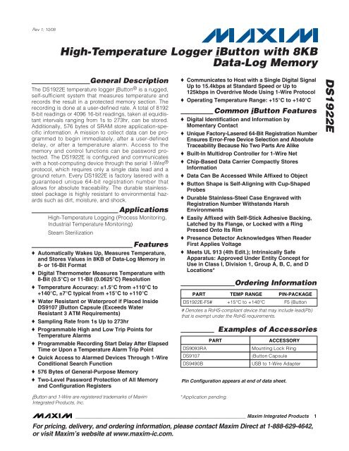
DS1922E High-Temperature Logger iButton with 8KB Data-Log ...
DS1922E High-Temperature Logger iButton with 8KB Data-Log ...
DS1922E High-Temperature Logger iButton with 8KB Data-Log ...

You also want an ePaper? Increase the reach of your titles
YUMPU automatically turns print PDFs into web optimized ePapers that Google loves.
Rev 1; 10/08<br />
<strong>High</strong>-<strong>Temperature</strong> <strong><strong>Log</strong>ger</strong> <strong>iButton</strong> <strong>with</strong> <strong>8KB</strong><br />
<strong>Data</strong>-<strong>Log</strong> Memory<br />
General Description<br />
The <strong>DS1922E</strong> temperature logger <strong>iButton</strong> ® is a rugged,<br />
self-sufficient system that measures temperature and<br />
records the result in a protected memory section. The<br />
recording is done at a user-defined rate. A total of 8192<br />
8-bit readings or 4096 16-bit readings, taken at equidistant<br />
intervals ranging from 1s to 273hr, can be stored.<br />
Additionally, 576 bytes of SRAM store application-specific<br />
information. A mission to collect data can be programmed<br />
to begin immediately, after a user-defined<br />
delay, or after a temperature alarm. Access to the<br />
memory and control functions can be password protected.<br />
The <strong>DS1922E</strong> is configured and communicates<br />
<strong>with</strong> a host-computing device through the serial 1-Wire ®<br />
protocol, which requires only a single data lead and a<br />
ground return. Every <strong>DS1922E</strong> is factory lasered <strong>with</strong> a<br />
guaranteed unique 64-bit registration number that<br />
allows for absolute traceability. The durable stainlesssteel<br />
package is highly resistant to environmental hazards<br />
such as dirt, moisture, and shock.<br />
Applications<br />
<strong>High</strong>-<strong>Temperature</strong> <strong>Log</strong>ging (Process Monitoring,<br />
Industrial <strong>Temperature</strong> Monitoring)<br />
Steam Sterilization<br />
Features<br />
♦ Automatically Wakes Up, Measures <strong>Temperature</strong>,<br />
and Stores Values in <strong>8KB</strong> of <strong>Data</strong>-<strong>Log</strong> Memory in<br />
8- or 16-Bit Format<br />
♦ Digital Thermometer Measures <strong>Temperature</strong> <strong>with</strong><br />
8-Bit (0.5°C) or 11-Bit (0.0625°C) Resolution<br />
♦ <strong>Temperature</strong> Accuracy: ±1.5°C from +110°C to<br />
+140°C, ±7°C typical from +15°C to +110°C<br />
♦ Water Resistant or Waterproof if Placed Inside<br />
DS9107 <strong>iButton</strong> Capsule (Exceeds Water<br />
Resistant 3 ATM Requirements)<br />
♦ Sampling Rate from 1s Up to 273hr<br />
♦ Programmable <strong>High</strong> and Low Trip Points for<br />
<strong>Temperature</strong> Alarms<br />
♦ Programmable Recording Start Delay After Elapsed<br />
Time or Upon a <strong>Temperature</strong> Alarm Trip Point<br />
♦ Quick Access to Alarmed Devices Through 1-Wire<br />
Conditional Search Function<br />
♦ 576 Bytes of General-Purpose Memory<br />
♦ Two-Level Password Protection of All Memory<br />
and Configuration Registers<br />
<strong>iButton</strong> and 1-Wire are registered trademarks of Maxim<br />
Integrated Products, Inc.<br />
♦ Communicates to Host <strong>with</strong> a Single Digital Signal<br />
Up to 15.4kbps at Standard Speed or Up to<br />
125kbps in Overdrive Mode Using 1-Wire Protocol<br />
♦ Operating <strong>Temperature</strong> Range: +15°C to +140°C<br />
Common <strong>iButton</strong> Features<br />
♦ Digital Identification and Information by<br />
Momentary Contact<br />
♦ Unique Factory-Lasered 64-Bit Registration Number<br />
Ensures Error-Free Device Selection and Absolute<br />
Traceability Because No Two Parts Are Alike<br />
♦ Built-In Multidrop Controller for 1-Wire Net<br />
♦ Chip-Based <strong>Data</strong> Carrier Compactly Stores<br />
Information<br />
♦ <strong>Data</strong> Can Be Accessed While Affixed to Object<br />
♦ Button Shape is Self-Aligning <strong>with</strong> Cup-Shaped<br />
Probes<br />
♦ Durable Stainless-Steel Case Engraved <strong>with</strong><br />
Registration Number Withstands Harsh<br />
Environments<br />
♦ Easily Affixed <strong>with</strong> Self-Stick Adhesive Backing,<br />
Latched by Its Flange, or Locked <strong>with</strong> a Ring<br />
Pressed Onto Its Rim<br />
♦ Presence Detector Acknowledges When Reader<br />
First Applies Voltage<br />
♦ Meets UL 913 (4th Edit.); Intrinsically Safe<br />
Apparatus: Approved Under Entity Concept for<br />
Use in Class I, Division 1, Group A, B, C, and D<br />
Locations*<br />
*Application pending.<br />
Ordering Information<br />
PART TEMP RANGE PIN-PACKAGE<br />
<strong>DS1922E</strong>-F5# +15°C to +140°C F5 <strong>iButton</strong><br />
# Denotes a RoHS-compliant device that may include lead(Pb)<br />
that is exempt under the RoHS requirements.<br />
Examples of Accessories<br />
PART ACCESSORY<br />
DS9093RA Mounting Lock Ring<br />
DS9107 <strong>iButton</strong> Capsule<br />
DS9490B USB to 1-Wire Adapter<br />
Pin Configuration appears at end of data sheet.<br />
________________________________________________________________ Maxim Integrated Products 1<br />
For pricing, delivery, and ordering information, please contact Maxim Direct at 1-888-629-4642,<br />
or visit Maxim’s website at www.maxim-ic.com.<br />
<strong>DS1922E</strong>
<strong>DS1922E</strong><br />
<strong>High</strong>-<strong>Temperature</strong> <strong><strong>Log</strong>ger</strong> <strong>iButton</strong> <strong>with</strong> <strong>8KB</strong><br />
<strong>Data</strong>-<strong>Log</strong> Memory<br />
ABSOLUTE MAXIMUM RATINGS<br />
I/O Voltage Range to GND .......................................-0.3V to +6V<br />
I/O Sink Current...................................................................20mA<br />
Operating <strong>Temperature</strong> Range ........................+15°C to +140°C<br />
Stresses beyond those listed under “Absolute Maximum Ratings” may cause permanent damage to the device. These are stress ratings only, and functional<br />
operation of the device at these or any other conditions beyond those indicated in the operational sections of the specifications is not implied. Exposure to<br />
absolute maximum rating conditions for extended periods may affect device reliability.<br />
ELECTRICAL CHARACTERISTICS<br />
(VPUP = 3.0V to 5.25V.)<br />
Junction <strong>Temperature</strong>......................................................+150°C<br />
Storage <strong>Temperature</strong> Range...........................+15°C to +140°C*<br />
*Storage or operation above +50°C significantly reduces battery life <strong>with</strong> an upper limit of 300hr cumulative at +140°C.<br />
PARAMETER SYMBOL CONDITIONS MIN TYP MAX UNITS<br />
Operating <strong>Temperature</strong> TA <strong>DS1922E</strong> (Note 1) +15 +140 °C<br />
I/O PIN GENERAL DATA<br />
1-Wire Pullup Resistance RPUP (Notes 2, 3) 2.2 k<br />
Input Capacitance CIO (Note 4) 100 800 pF<br />
Input Load Current IL I/O pin at VPUP 6 10 μA<br />
<strong>High</strong>-to-Low Switching Threshold VTL (Notes 5, 6) 0.4 3.2 V<br />
Input Low Voltage VIL (Notes 2, 7) 0.3 V<br />
Low-to-<strong>High</strong> Switching Threshold VTH (Notes 5, 8) 0.7 3.4 V<br />
Switching Hysteresis VHY (Note 9) 0.09 N/A V<br />
Output Low Voltage VOL At 4mA (Note 10) 0.4 V<br />
Recovery Time<br />
(Note 2)<br />
tREC<br />
Standard speed, RPUP = 2.2k 5<br />
Overdrive speed, RPUP = 2.2k 2<br />
Overdrive speed, directly prior to reset<br />
pulse; RPUP = 2.2k<br />
Rising-Edge Hold-Off Time tREH (Note 11) 0.6 2.0 μs<br />
Time Slot Duration (Note 2) tSLOT<br />
I/O PIN 1-Wire RESET, PRESENCE-DETECT CYCLE<br />
Reset Low Time (Note 2) tRSTL<br />
Presence-Detect <strong>High</strong> Time tPDH<br />
Standard speed 65<br />
Overdrive speed, VPUP > 4.5V 8<br />
Overdrive speed (Note 12) 9.5<br />
Standard speed, VPUP > 4.5V 480 720<br />
Standard speed (Note 12) 690 720<br />
Overdrive speed, VPUP > 4.5V 48 80<br />
Overdrive speed (Note 12) 70 80<br />
Standard speed, VPUP > 4.5V 15 60<br />
Standard speed (Note 12) 15 63.5<br />
Overdrive speed (Note 12) 2 7<br />
2 _______________________________________________________________________________________<br />
5<br />
μs<br />
μs<br />
μs<br />
μs
<strong>High</strong>-<strong>Temperature</strong> <strong><strong>Log</strong>ger</strong> <strong>iButton</strong> <strong>with</strong> <strong>8KB</strong><br />
<strong>Data</strong>-<strong>Log</strong> Memory<br />
ELECTRICAL CHARACTERISTICS (continued)<br />
(VPUP = 3.0V to 5.25V.)<br />
PARAMETER SYMBOL CONDITIONS MIN TYP MAX UNITS<br />
Presence-Detect Fall Time<br />
(Note 13)<br />
tFPD<br />
Presence-Detect Low Time tPDL<br />
Presence-Detect Sample Time<br />
(Note 2)<br />
I/O PIN 1-Wire WRITE<br />
Write-Zero Low Time<br />
(Notes 2, 14)<br />
Write-One Low Time<br />
(Notes 2, 14)<br />
I/O PIN 1-Wire READ<br />
Read Low Time<br />
(Notes 2, 15)<br />
Read Sample Time<br />
(Notes 2, 15)<br />
REAL-TIME CLOCK (RTC)<br />
Accuracy<br />
tMSP<br />
tW0L<br />
tW1L<br />
tRL<br />
tMSR<br />
Standard speed, VPUP > 4.5V 1.5 5<br />
Standard speed 1.5 8<br />
Overdrive speed 0.15 1<br />
Standard speed, VPUP > 4.5V 60 240<br />
Standard speed (Note 12) 60 287<br />
Overdrive speed, VPUP > 4.5V (Note 12) 7 24<br />
Overdrive speed (Note 12) 7 28<br />
Standard speed, VPUP > 4.5V 65 75<br />
Standard speed 71.5 75<br />
Overdrive speed 8 9<br />
Standard speed 60 120<br />
Overdrive speed, VPUP > 4.5V (Note 12) 6 12<br />
Overdrive speed (Note 12) 7.5 12<br />
Standard speed 5 15<br />
Overdrive speed 1 1.95<br />
Standard speed 5 15 - <br />
Overdrive speed 1 1.95 - <br />
Standard speed tRL + 15<br />
Overdrive speed tRL + 1.95<br />
See the RTC Accuracy<br />
graph<br />
Frequency Deviation F 0°C to +125°C -600 +60 ppm<br />
TEMPERATURE CONVERTER<br />
Conversion Time<br />
(Note 16)<br />
Thermal Response Time<br />
Constant (Note 17)<br />
tCONV<br />
Conversion Error (Notes 18, 19) <br />
<strong>Temperature</strong> Cycles NTCY<br />
8-bit mode 30 75<br />
16-bit mode (11 bits) 240 600<br />
RESP <strong>iButton</strong> package 130 s<br />
+15°C to +110°C (Note 20) ±7<br />
+110°C to +140°C -1.5 +1.5<br />
Cycle = ramp from +25°C to > +125°C<br />
and back to +25°C (Note 21)<br />
_______________________________________________________________________________________ 3<br />
μs<br />
μs<br />
μs<br />
μs<br />
μs<br />
μs<br />
μs<br />
Min/<br />
Month<br />
ms<br />
°C<br />
300 Cycles<br />
Operating Lifetime tLIFE <strong>Temperature</strong> > +125°C (Note 21) 300 Hours<br />
<strong>DS1922E</strong>
<strong>DS1922E</strong><br />
<strong>High</strong>-<strong>Temperature</strong> <strong><strong>Log</strong>ger</strong> <strong>iButton</strong> <strong>with</strong> <strong>8KB</strong><br />
<strong>Data</strong>-<strong>Log</strong> Memory<br />
Note 1: Operation above +125°C is restricted to mission operations only. Communication and 1-Wire pin specifications are not<br />
specified for operation above +125°C.<br />
Note 2: System requirement.<br />
Note 3: Maximum allowable pullup resistance is a function of the number of 1-Wire devices in the system and 1-Wire recovery<br />
times. The specified value here applies to systems <strong>with</strong> only one device and <strong>with</strong> the minimum 1-Wire recovery times. For<br />
more heavily loaded systems, an active pullup such as that in the DS2480B can be required.<br />
Note 4: Capacitance on the data pin could be 800pF when VPUP is first applied. If a 2.2kΩ resistor is used to pull up the data line<br />
2.5µs after VPUP has been applied, the parasite capacitance does not affect normal communications.<br />
Note 5: VTL and VTH are a function of the internal supply voltage, which is a function of VPUP and the 1-Wire recovery times. The<br />
VTH and VTL maximum specifications are valid at VPUPMAX (5.25V). In any case, VTL < VTH < VPUP.<br />
Note 6: Voltage below which, during a falling edge on I/O, a logic 0 is detected.<br />
Note 7: The voltage on I/O must be less than or equal to VILMAX whenever the master drives the line low.<br />
Note 8: Voltage above which, during a rising edge on I/O, a logic 1 is detected.<br />
Note 9: After VTH is crossed during a rising edge on I/O, the voltage on I/O must drop by VHY to be detected as logic 0.<br />
Note 10: The I-V characteristic is linear for voltages less than 1V.<br />
Note 11: The earliest recognition of a negative edge is possible at tREH after VTH has been previously reached.<br />
Note 12: Numbers in bold are not in compliance <strong>with</strong> the published <strong>iButton</strong> standards. See the Comparison Table.<br />
Note 13: Interval during the negative edge on I/O at the beginning of a presence-detect pulse between the time at which the voltage<br />
is 90% of VPUP and the time at which the voltage is 10% of VPUP.<br />
Note 14: ε in Figure 13 represents the time required for the pullup circuitry to pull the voltage on I/O up from VIL to VTH. The actual<br />
maximum duration for the master to pull the line low is tW1LMAX + tF - ε and tW0LMAX + tF - ε, respectively.<br />
Note 15: δ in Figure 13 represents the time required for the pullup circuitry to pull the voltage on I/O up from VIL to the input high<br />
threshold of the bus master. The actual maximum duration for the master to pull the line low is tRLMAX + tF.<br />
Note 16: To conserve battery power, use 8-bit temperature logging whenever possible.<br />
Note 17: This number was derived from a test conducted by Cemagref in Antony, France, in July 2000:<br />
www.cemagref.fr/English/index.htm Test Report No. E42.<br />
Note 18: Includes +0.1°C/-0.2°C calibration chamber measurement uncertainty.<br />
Note 19: Warning: Not for use as the sole method of measuring or tracking temperature in products and articles that could affect<br />
the health or safety of persons, plants, animals, or other living organisms, including but not limited to foods, beverages,<br />
pharmaceuticals, medications, blood and blood products, organs, and flammable and combustible products. User shall<br />
assure that redundant (or other primary) methods of testing and determining the handling methods, quality, and fitness of<br />
the articles and products should be implemented. <strong>Temperature</strong> tracking <strong>with</strong> this product, where the health or safety of<br />
the aforementioned persons or things could be adversely affected, is only recommended when supplemental or redundant<br />
information sources are used. <strong>Data</strong>-logger products are 100% tested and calibrated at time of manufacture by<br />
Maxim to ensure that they meet all data sheet parameters, including temperature accuracy. User shall be responsible for<br />
proper use and storage of this product. As <strong>with</strong> any sensor-based product, user shall also be responsible for occasionally<br />
rechecking the temperature accuracy of the product to ensure it is still operating properly.<br />
Note 20: Guaranteed by design and not production tested.<br />
Note 21: Devices leave the factory after having been run through a few cycles above +125°C. This is required for calibration of the<br />
device but should not affect lifetime of the device as specified. However, this process results in a nonzero value in the<br />
Device Samples Counter register (0223h–0225h), which provides evidence the device has been factory calibrated.<br />
4 _______________________________________________________________________________________
PARAMETER<br />
<strong>High</strong>-<strong>Temperature</strong> <strong><strong>Log</strong>ger</strong> <strong>iButton</strong> <strong>with</strong> <strong>8KB</strong><br />
<strong>Data</strong>-<strong>Log</strong> Memory<br />
STANDARD SPEED<br />
(μs)<br />
LEGACY VALUES <strong>DS1922E</strong> VALUES<br />
OVERDRIVE SPEED<br />
(μs)<br />
STANDARD SPEED<br />
(μs)<br />
Comparison Table<br />
OVERDRIVE SPEED<br />
(μs)<br />
MIN MAX MIN MAX MIN MAX MIN MAX<br />
tSLOT (including tREC) 61 (undefined) 7 (undefined) 65 * (undefined) 9.5 (undefined)<br />
tRSTL 480 (undefined) 48 80 690 720 70 80<br />
tPDH 15 60 2 6 15 63.5 2 7<br />
tPDL 60 240 8 24 60 287 7 28<br />
tW0L 60 120 6 16 60 120 7.5 12<br />
*Intentional change; longer recovery time requirement due to modified 1-Wire front-end.<br />
Note: Numbers in bold are not in compliance <strong>with</strong> the published <strong>iButton</strong> standards.<br />
SIZE See the Package Information section.<br />
WEIGHT Ca. 3.3 grams<br />
<strong>iButton</strong> Can Physical Specification<br />
Meets UL 913 (4th Edit.); Intrinsically Safe Apparatus, approval under Entity Concept for use in Class I,<br />
SAFETY<br />
Division 1, Group A, B, C, and D Locations*.<br />
*Application pending.<br />
DRIFT (MINUTES/MONTH)<br />
2<br />
0<br />
-2<br />
-4<br />
-6<br />
-8<br />
-10<br />
-12<br />
-14<br />
-16<br />
RTC ACCURACY (TYPICAL)<br />
-18<br />
15 25 35 45 55 65 75 85 95 105 115 125 135<br />
TEMPERATURE (°C)<br />
RTC Accuracy<br />
_______________________________________________________________________________________ 5<br />
<strong>DS1922E</strong>
<strong>DS1922E</strong><br />
<strong>High</strong>-<strong>Temperature</strong> <strong><strong>Log</strong>ger</strong> <strong>iButton</strong> <strong>with</strong> <strong>8KB</strong><br />
<strong>Data</strong>-<strong>Log</strong> Memory<br />
Detailed Description<br />
With its extended temperature range, the <strong>DS1922E</strong> is<br />
well suited to monitor processes that require temperatures<br />
well above the boiling point of water, such as pasteurization<br />
of food items. Note that the initial sealing<br />
level of the <strong>DS1922E</strong> achieves the equivalent of IP56.<br />
Aging and use conditions can degrade the integrity of<br />
the seal over time, so for applications <strong>with</strong> significant<br />
exposure to liquids, sprays, or other similar environments,<br />
it is recommended to place the <strong>DS1922E</strong> in the<br />
DS9107 <strong>iButton</strong> capsule. The DS9107 provides a watertight<br />
enclosure that has been rated to IP68 (refer to<br />
Application Note 4126: Understanding the IP (Ingress<br />
Protection) Ratings of <strong>iButton</strong> <strong>Data</strong> <strong><strong>Log</strong>ger</strong>s and<br />
Capsules). Software for setup and data retrieval through<br />
the 1-Wire interface is available for free download from<br />
the <strong>iButton</strong> website (www.ibutton.com). This software<br />
also includes drivers for the serial and USB port of a PC<br />
and routines to access the general-purpose memory for<br />
storing application- or equipment-specific data files.<br />
Overview<br />
The block diagram in Figure 1 shows the relationships<br />
between the major control and memory sections of the<br />
<strong>DS1922E</strong>. The device has five main data components:<br />
64-bit lasered ROM; 256-bit scratchpad; 576-byte general-purpose<br />
SRAM; two 256-bit register pages of timekeeping,<br />
control, status, and counter registers, and<br />
passwords; and 8192 bytes of data-logging memory.<br />
Except for the ROM and the scratchpad, all other memory<br />
is arranged in a single linear address space. The<br />
data-logging memory, counter registers, and several<br />
other registers are read only for the user. Both register<br />
pages are write protected while the device is programmed<br />
for a mission. The password registers, one for<br />
a read password and another one for a read/write password,<br />
can only be written, never read.<br />
Figure 2 shows the hierarchical structure of the 1-Wire<br />
protocol. The bus master must first provide one of the<br />
eight ROM function commands: Read ROM, Match<br />
ROM, Search ROM, Conditional Search ROM, Skip<br />
ROM, Overdrive-Skip ROM, Overdrive-Match ROM, or<br />
Resume Command. Upon completion of an Overdrive<br />
ROM command byte executed at standard speed, the<br />
device enters Overdrive Mode, where all subsequent<br />
communication occurs at a higher speed. The protocol<br />
required for these ROM function commands is<br />
described in Figure 11. After a ROM function command<br />
is successfully executed, the memory and control functions<br />
become accessible and the master can provide<br />
any one of the eight available commands. The protocol<br />
for these memory and control function commands is<br />
described in Figure 9. All data is read and written<br />
least significant bit first.<br />
Parasite Power<br />
The block diagram (Figure 1) shows the parasite-powered<br />
circuitry. This circuitry “steals” power whenever the<br />
I/O input is high. I/O provides sufficient power as long as<br />
the specified timing and voltage requirements are met.<br />
The advantages of parasite power are two-fold: 1) By<br />
parasiting off this input, battery power is not consumed<br />
for 1-Wire ROM function commands, and 2) if the battery<br />
is exhausted for any reason, the ROM can still be read<br />
normally. The remaining circuitry of the <strong>DS1922E</strong> is solely<br />
operated by battery energy.<br />
64-Bit Lasered ROM<br />
Each <strong>DS1922E</strong> contains a unique ROM code that is 64<br />
bits long. The first 8 bits are a 1-Wire family code. The<br />
next 48 bits are a unique serial number. The last 8 bits<br />
are a cyclic redundancy check (CRC) of the first 56 bits<br />
(see Figure 3 for details). The 1-Wire CRC is generated<br />
using a polynomial generator consisting of a shift register<br />
and XOR gates as shown in Figure 4. The polynomial<br />
is X8 + X5 + X4 + 1. Additional information about the<br />
1-Wire CRC is available in Application Note 27:<br />
Understanding and Using Cyclic Redundancy Checks<br />
<strong>with</strong> Maxim <strong>iButton</strong> Products.<br />
The shift register bits are initialized to 0. Then, starting<br />
<strong>with</strong> the least significant bit of the family code, one bit<br />
at a time is shifted in. After the 8th bit of the family code<br />
has been entered, the serial number is entered. After<br />
the last bit of the serial number has been entered, the<br />
shift register contains the CRC value. Shifting in the 8<br />
bits of CRC returns the shift register to all 0s.<br />
6 _______________________________________________________________________________________
Figure 1. Block Diagram<br />
<strong>High</strong>-<strong>Temperature</strong> <strong><strong>Log</strong>ger</strong> <strong>iButton</strong> <strong>with</strong> <strong>8KB</strong><br />
<strong>Data</strong>-<strong>Log</strong> Memory<br />
3V LITHIUM<br />
1-Wire PORT<br />
32.768kHz<br />
OSCILLATOR<br />
THERMAL<br />
SENSE<br />
I/O<br />
ADC<br />
<strong>DS1922E</strong><br />
CONTROL<br />
LOGIC<br />
ROM<br />
FUNCTION<br />
CONTROL<br />
INTERNAL<br />
TIMEKEEPING,<br />
CONTROL REGISTERS,<br />
AND COUNTERS<br />
64-BIT<br />
LASERED<br />
ROM<br />
MEMORY<br />
FUNCTION<br />
CONTROL<br />
GENERAL-PURPOSE<br />
SRAM<br />
(512 BYTES)<br />
REGISTER PAGES<br />
(64 BYTES)<br />
USER MEMORY<br />
(64 BYTES)<br />
DATA-LOG MEMORY<br />
<strong>8KB</strong><br />
PARASITE-POWERED<br />
CIRCUITRY<br />
256-BIT<br />
SCRATCHPAD<br />
_______________________________________________________________________________________ 7<br />
<strong>DS1922E</strong>
<strong>DS1922E</strong><br />
<strong>High</strong>-<strong>Temperature</strong> <strong><strong>Log</strong>ger</strong> <strong>iButton</strong> <strong>with</strong> <strong>8KB</strong><br />
<strong>Data</strong>-<strong>Log</strong> Memory<br />
BUS<br />
MASTER<br />
COMMAND LEVEL:<br />
1-Wire ROM<br />
FUNCTION COMMANDS<br />
<strong>DS1922E</strong>-SPECIFIC<br />
MEMORY FUNCTION COMMANDS<br />
1-Wire NET<br />
Figure 2. Hierarchical Structure for 1-Wire Protocol<br />
MSB<br />
8-BIT<br />
CRC CODE<br />
MSB LSB MSB<br />
Figure 3. 64-Bit Lasered ROM<br />
1ST<br />
STAGE<br />
2ND<br />
STAGE<br />
3RD<br />
STAGE<br />
OTHER DEVICES<br />
AVAILABLE COMMANDS: DATA FIELD AFFECTED:<br />
READ ROM<br />
MATCH ROM<br />
SEARCH ROM<br />
CONDITIONAL SEARCH ROM<br />
SKIP ROM<br />
RESUME<br />
OVERDRIVE-SKIP ROM<br />
OVERDRIVE-MATCH ROM<br />
WRITE SCRATCHPAD<br />
READ SCRATCHPAD<br />
COPY SCRATCHPAD WITH PW<br />
READ MEMORY WITH PW AND CRC<br />
CLEAR MEMORY WITH PW<br />
FORCED CONVERSION<br />
START MISSION WITH PW<br />
STOP MISSION WITH PW<br />
4TH<br />
STAGE<br />
X 0 X 1 X 2 X 3 X 4<br />
Figure 4. 1-Wire CRC Generator<br />
<strong>DS1922E</strong><br />
48-BIT SERIAL NUMBER<br />
POLYNOMIAL = X 8 + X 5 + X 4 + 1<br />
5TH<br />
STAGE<br />
64-BIT ROM, RC-FLAG<br />
64-BIT ROM, RC-FLAG<br />
64-BIT ROM, RC-FLAG<br />
64-BIT ROM, RC-FLAG, ALARM FLAGS, SEARCH CONDITIONS<br />
RC-FLAG<br />
RC-FLAG<br />
RC-FLAG, OD-FLAG<br />
64-BIT ROM, RC-FLAG, OD-FLAG<br />
256-BIT SCRATCHPAD, FLAGS<br />
256-BIT SCRATCHPAD<br />
512-BYTE DATA MEMORY, REGISTERS, FLAGS, PASSWORDS<br />
MEMORY, REGISTERS, PASSWORDS<br />
MISSION TIMESTAMP, MISSION SAMPLES COUNTER,<br />
START DELAY, ALARM FLAGS, PASSWORDS<br />
MEMORY ADDRESSES 020Ch TO 020Dh<br />
FLAGS, TIMESTAMP, MEMORY ADDRESSES<br />
020Ch TO 020Dh (WHEN LOGGING)<br />
FLAGS<br />
6TH<br />
STAGE<br />
8-BIT FAMILY CODE<br />
(41h)<br />
8 _______________________________________________________________________________________<br />
LSB<br />
MSB<br />
7TH<br />
STAGE<br />
8TH<br />
STAGE<br />
INPUT DATA<br />
LSB<br />
LSB<br />
X 5 X 6 X 7 X 8
<strong>High</strong>-<strong>Temperature</strong> <strong><strong>Log</strong>ger</strong> <strong>iButton</strong> <strong>with</strong> <strong>8KB</strong><br />
<strong>Data</strong>-<strong>Log</strong> Memory<br />
Memory<br />
Figure 5 shows the <strong>DS1922E</strong> memory map. Pages 0 to<br />
15 contain 512 bytes of general-purpose SRAM. The<br />
various registers to set up and control the device fill<br />
pages 16 and 17, called register pages 1 and 2 (see<br />
Figure 6 for details). Pages 18 and 19 can be used as<br />
extension of the general-purpose memory. The data-log<br />
logging memory starts at address 1000h (page 128)<br />
and extends over 256 pages. The memory pages 20 to<br />
127 are reserved for future extensions. The scratchpad<br />
is an additional page that acts as a buffer when writing<br />
to the SRAM memory or the register page. The data<br />
Figure 5. Memory Map<br />
ADDRESS<br />
0000h TO 001Fh<br />
32-BYTE INTERMEDIATE STORAGE<br />
SCRATCHPAD<br />
32-BYTE GENERAL-PURPOSE SRAM<br />
(R/W)<br />
memory can be written at any time. The access type for<br />
the register pages is register-specific and depends on<br />
whether the device is programmed for a mission.<br />
Figure 6 shows the details. The data-log memory is<br />
read only for the user. It is written solely under supervision<br />
of the on-chip control logic. Due to the special<br />
behavior of the write access logic (write scratchpad,<br />
copy scratchpad), it is recommended to only write full<br />
pages at a time. This also applies to the register pages.<br />
See the Address Registers and Transfer Status section<br />
for details.<br />
PAGE 0<br />
0020h TO 01FFh GENERAL-PURPOSE SRAM (R/W) PAGES 1 TO 15<br />
0200h TO 021Fh 32-BYTE REGISTER PAGE 1 PAGE 16<br />
0220h TO 023Fh 32-BYTE REGISTER PAGE 2 PAGE 17<br />
0240h TO 025Fh GENERAL-PURPOSE SRAM (R/W) PAGE 18<br />
0260h TO 027Fh GENERAL-PURPOSE SRAM (R/W) PAGE 19<br />
0280h TO 0FFFh (RESERVED FOR FUTURE EXTENSIONS) PAGES 20 TO 127<br />
1000h TO 2FFFh DATA-LOG MEMORY (READ ONLY) PAGES 128 TO 383<br />
_______________________________________________________________________________________ 9<br />
<strong>DS1922E</strong>
<strong>DS1922E</strong><br />
<strong>High</strong>-<strong>Temperature</strong> <strong><strong>Log</strong>ger</strong> <strong>iButton</strong> <strong>with</strong> <strong>8KB</strong><br />
<strong>Data</strong>-<strong>Log</strong> Memory<br />
ADDRESS BIT 7 BIT 6 BIT 5 BIT 4 BIT 3 BIT 2 BIT 1 BIT 0 FUNCTION ACCESS*<br />
0200h 0 10 Seconds Single Seconds<br />
0201h 0 10 Minutes Single Minutes<br />
0202h 0 12/24<br />
20 Hour<br />
AM/PM<br />
10 Hour Single Hours<br />
0203h 0 0 10 Date Single Date<br />
0204h CENT 0 0<br />
10<br />
Months<br />
Single Months<br />
0205h 10 Years Single Years<br />
0206h Low Byte<br />
0207h 0 0 <strong>High</strong> Byte<br />
0208h Low Threshold<br />
0209h <strong>High</strong> Threshold<br />
020Ah (No Function <strong>with</strong> the <strong>DS1922E</strong>)<br />
020Bh (No Function <strong>with</strong> the <strong>DS1922E</strong>)<br />
020Ch Low Byte 0 0 0 0 0<br />
020Dh <strong>High</strong> Byte<br />
020Eh (No Function <strong>with</strong> the <strong>DS1922E</strong>)<br />
020Fh (No Function <strong>with</strong> the <strong>DS1922E</strong>)<br />
0210h 0 0 0 0 0 0 ETHA ETLA<br />
Real-<br />
Time Clock<br />
Registers<br />
Sample<br />
Rate<br />
<strong>Temperature</strong><br />
Alarms<br />
10 ______________________________________________________________________________________<br />
R/W R<br />
R/W R<br />
R/W R<br />
— R/W R<br />
Latest<br />
<strong>Temperature</strong><br />
R R<br />
— R R<br />
<strong>Temperature</strong><br />
Alarm<br />
Enable<br />
R/W R<br />
0211h 1 1 1 1 1 1 0 0 — R/W R<br />
0212h 0 0 0 0 0 0 EHSS EOSC RTC Control R/W R<br />
0213h 1 1 SUTA RO (X) TLFS 0 ETL<br />
Mission<br />
Control<br />
R/W R<br />
0214h BOR 1 1 1 0 0 THF TLF Alarm Status R R<br />
0215h 1 1 0 WFTA MEMCLR 0 MIP 0<br />
0216h Low Byte<br />
0217h Center Byte<br />
0218h <strong>High</strong> Byte<br />
Figure 6. <strong>DS1922E</strong> Register Pages Map<br />
General<br />
Status<br />
Start<br />
Delay<br />
Counter<br />
R R<br />
R/W R<br />
*The left entry in the ACCESS column is valid between missions. The right entry shows the applicable access type while a<br />
mission is in progress.
<strong>High</strong>-<strong>Temperature</strong> <strong><strong>Log</strong>ger</strong> <strong>iButton</strong> <strong>with</strong> <strong>8KB</strong><br />
<strong>Data</strong>-<strong>Log</strong> Memory<br />
ADDRESS BIT 7 BIT 6 BIT 5 BIT 4 BIT 3 BIT 2 BIT 1 BIT 0 FUNCTION ACCESS*<br />
0219h 0 10 Seconds Single Seconds<br />
021Ah 0 10 Minutes Single Minutes<br />
021Bh 0 12/24<br />
20 Hour<br />
AM/PM<br />
10 Hour Single Hours<br />
021Ch 0 0 10 Date Single Date<br />
021Dh CENT 0 0<br />
10<br />
Months<br />
Single Months<br />
021Eh 10 Years Single Years<br />
Mission<br />
Timestamp<br />
R R<br />
021Fh (No Function; Reads 00h) — R R<br />
0220h Low Byte<br />
0221h Center Byte<br />
0222h <strong>High</strong> Byte<br />
0223h Low Byte<br />
0224h Center Byte<br />
0225h <strong>High</strong> Byte<br />
Mission<br />
Samples<br />
Counter<br />
Device<br />
Samples<br />
Counter<br />
R R<br />
R R<br />
0226h Configuration Code Flavor R R<br />
0227h EPW PW Control R/W R<br />
0228h First Byte<br />
… …<br />
022Fh Eighth Byte<br />
0230h First Byte<br />
… …<br />
0237h Eighth Byte<br />
0238h<br />
…<br />
023Fh<br />
Read<br />
Access<br />
Password<br />
Full<br />
Access<br />
Password<br />
W —<br />
W —<br />
(No Function; All These Bytes Read 00h) — R R<br />
*The left entry in the ACCESS column is valid between missions. The right entry shows the applicable access type while a<br />
mission is in progress.<br />
Figure 6. <strong>DS1922E</strong> Register Pages Map (continued)<br />
______________________________________________________________________________________ 11<br />
<strong>DS1922E</strong>
<strong>DS1922E</strong><br />
<strong>High</strong>-<strong>Temperature</strong> <strong><strong>Log</strong>ger</strong> <strong>iButton</strong> <strong>with</strong> <strong>8KB</strong><br />
<strong>Data</strong>-<strong>Log</strong> Memory<br />
Detailed Register Descriptions<br />
Timekeeping and Calendar<br />
The RTC and calendar information is accessed by<br />
reading/writing the appropriate bytes in the register<br />
page, address 0200h to 0205h. For readings to be<br />
valid, all RTC registers must be read sequentially starting<br />
at address 0200h. Some of the RTC bits are set to<br />
0. These bits always read 0 regardless of how they are<br />
written. The number representation of the RTC registers<br />
is binary-coded decimal (BCD) format.<br />
The <strong>DS1922E</strong>’s RTC can run in either 12hr or 24hr<br />
mode. Bit 6 of the Hours register (address 0202h) is<br />
defined as the 12hr or 24hr mode select bit. When high,<br />
the 12hr mode is selected. In the 12hr mode, bit 5 is<br />
the AM/PM bit <strong>with</strong> logic 1 being PM. In the 24hr mode,<br />
bit 5 is the 20hr bit (20hr to 23hr). The CENT bit, bit 7 of<br />
the Months register, can be written by the user. This bit<br />
changes its state when the years counter transitions<br />
from 99 to 00.<br />
The calendar logic is designed to automatically compensate<br />
for leap years. For every year value that is<br />
either 00 or a multiple of 4, the device adds a 29th of<br />
February. This works correctly up to (but not including)<br />
the year 2100.<br />
Sample Rate<br />
The content of the Sample Rate register (addresses<br />
0206h, 0207h) specifies the time elapse (in seconds if<br />
EHSS = 1, or minutes if EHSS = 0) between two temperature-logging<br />
events. The sample rate can be any<br />
value from 1 to 16,383, coded as an unsigned 14-bit<br />
binary number. If EHSS = 1, the shortest time between<br />
logging events is 1s and the longest (sample rate =<br />
3FFFh) is 4.55hr. If EHSS = 0, the shortest is 1min and<br />
the longest time is 273.05hr (sample rate = 3FFFh). The<br />
EHSS bit is located in the RTC Control register at<br />
address 0212h. It is important that the user sets the<br />
EHSS bit accordingly while setting the Sample Rate<br />
register. Writing a sample rate of 0000h results in a<br />
sample rate = 0001h, causing the <strong>DS1922E</strong> to log<br />
the temperature either every minute or every second<br />
depending upon the state of the EHSS bit.<br />
12 ______________________________________________________________________________________<br />
Sample Rate Register<br />
ADDRESS BIT 7 BIT 6 BIT 5 BIT 4 BIT 3 BIT 2 BIT 1 BIT 0<br />
0206h Sample Rate Low<br />
0207h 0 0 Sample Rate <strong>High</strong><br />
RTC Registers<br />
ADDRESS BIT 7 BIT 6 BIT 5 BIT 4 BIT 3 BIT 2 BIT 1 BIT 0<br />
0200h 0 10 Seconds Single Seconds<br />
0201h 0 10 Minutes Single Minutes<br />
0202h 0 12/24<br />
20 Hour<br />
AM/PM<br />
10 Hour Single Hours<br />
0203h 0 0 10 Date Single Date<br />
0204h CENT 0 0 10 Months Single Months<br />
0205h 10 Years Single Years<br />
Note: During a mission, there is only read access to these registers. Bit cells marked “0” always read 0 and cannot be written to 1.<br />
Note: During a mission, there is only read access to these registers. Bit cells marked “0” always read 0 and cannot be written to 1.
<strong>High</strong>-<strong>Temperature</strong> <strong><strong>Log</strong>ger</strong> <strong>iButton</strong> <strong>with</strong> <strong>8KB</strong><br />
<strong>Data</strong>-<strong>Log</strong> Memory<br />
<strong>Temperature</strong> Conversion<br />
The <strong>DS1922E</strong>’s temperature range begins at +15°C<br />
and ends at +140°C. <strong>Temperature</strong> values are represented<br />
as an 8- or 16-bit unsigned binary number <strong>with</strong><br />
a resolution of 0.5°C in 8-bit mode and 0.0625°C in<br />
16-bit mode.<br />
The higher temperature byte TRH is always valid. In<br />
16-bit mode, only the three highest bits of the lower<br />
byte TRL are valid. The five lower bits all read 0. TRL is<br />
undefined if the device is in 8-bit temperature mode. An<br />
out-of-range temperature reading is indicated as 00h or<br />
0000h when too cold and FFh or FFE0h when too hot.<br />
With TRH and TRL representing the decimal equivalent<br />
of a temperature reading, the temperature value is calculated<br />
as:<br />
ϑ(°C) = TRH/2 + 14 + TRL/512 (16-bit mode,<br />
TLFS = 1, see address 0213h)<br />
ϑ(°C) = TRH/2 + 14 (8-bit mode, TLFS = 0,<br />
see address 0213h)<br />
Latest <strong>Temperature</strong> Conversion Result Register<br />
ADDRESS BIT 7 BIT 6 BIT 5 BIT 4 BIT 3 BIT 2 BIT 1 BIT 0 BYTE<br />
020Ch T2 T1 T0 0 0 0 0 0 TRL<br />
020Dh T10 T9 T8 T7 T6 T5 T4 T3 TRH<br />
Table 1. <strong>Temperature</strong> Conversion Examples<br />
MODE<br />
TRH TRL<br />
This equation is valid for converting temperature readings<br />
stored in the data-log memory as well as for data<br />
read from the Latest <strong>Temperature</strong> Conversion Result<br />
register.<br />
To specify the temperature alarm thresholds, the previous<br />
equations are resolved to:<br />
TALM = 2 x ϑ(°C) - 28<br />
Because the temperature alarm threshold is only one<br />
byte, the resolution or temperature increment is limited<br />
to 0.5°C. The TALM value must be converted into hexadecimal<br />
format before it can be written to one of the<br />
<strong>Temperature</strong> Alarm Threshold registers (Low Alarm<br />
address 0208h; <strong>High</strong> Alarm address 0209h).<br />
Independent of the conversion mode (8- or 16-bit), only<br />
the most significant byte of a temperature conversion is<br />
used to determine whether an alarm is generated.<br />
HEX DECIMAL HEX DECIMAL<br />
8-Bit 54h 84 — — 56.0<br />
8-Bit 17h 23 — — 25.5<br />
16-Bit 54h 84 00h 0 56.0000<br />
16-Bit 17h 23 60h 96 25.6875<br />
Table 2. <strong>Temperature</strong> Alarm Threshold Examples<br />
(°C)<br />
TALM<br />
HEX DECIMAL<br />
65.5 67h 103<br />
30.0 20h 32<br />
______________________________________________________________________________________ 13<br />
(°C)<br />
<strong>DS1922E</strong>
<strong>DS1922E</strong><br />
<strong>High</strong>-<strong>Temperature</strong> <strong><strong>Log</strong>ger</strong> <strong>iButton</strong> <strong>with</strong> <strong>8KB</strong><br />
<strong>Data</strong>-<strong>Log</strong> Memory<br />
<strong>Temperature</strong> Sensor Alarm<br />
The <strong>DS1922E</strong> has two <strong>Temperature</strong> Alarm Threshold<br />
registers (address 0208h, 0209h) to store values that<br />
determine whether a critical temperature has been<br />
reached. A temperature alarm is generated if the<br />
device measures an alarming temperature and the<br />
alarm signaling is enabled. The bits ETLA and ETHA<br />
that enable the temperature alarm are located in the<br />
<strong>Temperature</strong> Sensor Control register. The temperature<br />
alarm flags TLF and THF are found in the Alarm Status<br />
register at address 0214h.<br />
Bit 1: Enable <strong>Temperature</strong> <strong>High</strong> Alarm (ETHA). This<br />
bit controls whether, during a mission, the temperature<br />
high alarm flag (THF) may be set, if a temperature conversion<br />
results in a value equal to or higher than the<br />
value in the <strong>Temperature</strong> <strong>High</strong> Alarm Threshold register.<br />
If ETHA is 1, temperature high alarms are enabled. If<br />
ETHA is 0, temperature high alarms are not generated.<br />
Bit 0: Enable <strong>Temperature</strong> Low Alarm (ETLA). This<br />
bit controls whether, during a mission, the temperature<br />
low alarm flag (TLF) may be set, if a temperature conversion<br />
results in a value equal to or lower than the<br />
value in the <strong>Temperature</strong> Low Alarm Threshold register.<br />
If ETLA is 1, temperature low alarms are enabled. If<br />
ETLA is 0, temperature low alarms are not generated.<br />
<strong>Temperature</strong> Sensor Control Register<br />
ADDRESS BIT 7 BIT 6 BIT 5 BIT 4 BIT 3 BIT 2 BIT 1 BIT 0<br />
0210h 0 0 0 0 0 0 ETHA ETLA<br />
Note: During a mission, there is only read access to this register. Bits 2 to 7 have no function. They always read 0 and cannot be<br />
written to 1.<br />
RTC Control<br />
To minimize the power consumption of a <strong>DS1922E</strong>, the<br />
RTC oscillator should be turned off when the device is<br />
not in use. The oscillator on/off bit is located in the RTC<br />
Control register. This register also includes the EHSS<br />
bit, which determines whether the sample rate is specified<br />
in seconds or minutes.<br />
Bit 1: Enable <strong>High</strong>-Speed Sample (EHSS). This bit<br />
controls the speed of the sample rate counter. When set<br />
to logic 0, the sample rate is specified in minutes. When<br />
set to logic 1, the sample rate is specified in seconds.<br />
Bit 0: Enable Oscillator (EOSC). This bit controls the<br />
crystal oscillator of the RTC. When set to logic 1, the<br />
oscillator starts. When written to logic 0, the oscillator<br />
stops and the device is in a low-power data-retention<br />
mode. This bit must be 1 for normal operation. A Forced<br />
Conversion or Start Mission command automatically<br />
starts the RTC by changing the EOSC bit to logic 1.<br />
14 ______________________________________________________________________________________<br />
RTC Control Register<br />
ADDRESS BIT 7 BIT 6 BIT 5 BIT 4 BIT 3 BIT 2 BIT 1 BIT 0<br />
0212h 0 0 0 0 0 0 EHSS EOSC<br />
Note: During a mission, there is only read access to this register. Bits 2 to 7 have no function. They always read 0 and cannot be<br />
written to 1.
<strong>High</strong>-<strong>Temperature</strong> <strong><strong>Log</strong>ger</strong> <strong>iButton</strong> <strong>with</strong> <strong>8KB</strong><br />
<strong>Data</strong>-<strong>Log</strong> Memory<br />
Mission Control<br />
The <strong>DS1922E</strong> is set up for its operation by writing<br />
appropriate data to its special function registers, which<br />
are located in the two register pages. The settings in<br />
the Mission Control register determine which format (8<br />
or 16 bits) applies and whether old data can be overwritten<br />
by new data once the data-log memory is full.<br />
An additional control bit can be set to tell the <strong>DS1922E</strong><br />
to wait <strong>with</strong> logging data until a temperature alarm is<br />
encountered.<br />
Bit 5: Start Mission Upon <strong>Temperature</strong> Alarm<br />
(SUTA). This bit specifies whether a mission begins<br />
immediately (includes delayed start) or if a temperature<br />
alarm is required to start the mission. If this bit is 1, the<br />
device performs an 8-bit temperature conversion at the<br />
selected sample rate and begins <strong>with</strong> data logging only<br />
if an alarming temperature (high alarm or low alarm)<br />
was found. The first logged temperature is when the<br />
alarm occurred. However, the mission sample counter<br />
does not increment. This functionality is guaranteed by<br />
design and not production tested.<br />
Mission Control Register<br />
ADDRESS BIT 7 BIT 6 BIT 5 BIT 4 BIT 3 BIT 2 BIT 1 BIT 0<br />
0213h 1 1 SUTA RO (X) TLFS 0 ETL<br />
Note: During a mission, there is only read access to this register. Bits 6 and 7 have no function. They always read 1 and cannot be<br />
written to 0. Bits 1 and 3 control functions that are not available <strong>with</strong> the <strong>DS1922E</strong>. Bit 1 must be set to 0. Under this condition the<br />
setting of bit 3 becomes a “don’t care.”<br />
Bit 4: Rollover Control (RO). This bit controls whether,<br />
during a mission, the data-log memory is overwritten<br />
<strong>with</strong> new data or whether data logging is stopped once<br />
the data-log memory is full. Setting this bit to 1 enables<br />
the rollover and data logging continues at the beginning,<br />
overwriting previously collected data. If this bit is<br />
0, the logging and conversions stop once the data-log<br />
memory is full. However, the RTC continues to run and<br />
the MIP bit remains set until the Stop Mission command<br />
is performed.<br />
Bit 2: <strong>Temperature</strong> <strong>Log</strong>ging Format Selection<br />
(TLFS). This bit specifies the format used to store temperature<br />
readings in the data-log memory. If this bit is<br />
0, the data is stored in 8-bit format. If this bit is 1, the<br />
16-bit format is used (higher resolution). With 16-bit format,<br />
the most significant byte is stored at the lower<br />
address.<br />
Bit 0: Enable <strong>Temperature</strong> <strong>Log</strong>ging (ETL). To set up<br />
the device for a temperature-logging mission, this bit<br />
must be set to logic 1. The recorded temperature values<br />
start at address 1000h.<br />
______________________________________________________________________________________ 15<br />
<strong>DS1922E</strong>
<strong>DS1922E</strong><br />
<strong>High</strong>-<strong>Temperature</strong> <strong><strong>Log</strong>ger</strong> <strong>iButton</strong> <strong>with</strong> <strong>8KB</strong><br />
<strong>Data</strong>-<strong>Log</strong> Memory<br />
Alarm Status<br />
The fastest way to determine whether a programmed<br />
temperature threshold was exceeded during a mission<br />
is through reading the Alarm Status register. In a networked<br />
environment that contains multiple <strong>DS1922E</strong><br />
<strong>iButton</strong>s, the devices that encountered an alarm can<br />
quickly be identified by means of the Conditional<br />
Search command (see the 1-Wire ROM Function<br />
Commands section). The temperature alarm only<br />
occurs if enabled (see the <strong>Temperature</strong> Sensor Alarm<br />
section). The BOR alarm is always enabled.<br />
Bit 7: Battery-On Reset Alarm (BOR). If this bit reads<br />
1, the device has performed a power-on reset. This<br />
indicates that the device has experienced a shock big<br />
enough to interrupt the internal battery power supply.<br />
The device may still appear functional, but it has lost its<br />
factory calibration. Any data found in the data-log<br />
memory should be disregarded.<br />
Bit 1: <strong>Temperature</strong> <strong>High</strong> Alarm Flag (THF). If this bit<br />
reads 1, there was at least one temperature conversion<br />
during a mission revealing a temperature equal to or<br />
higher than the value in the <strong>Temperature</strong> <strong>High</strong> Alarm<br />
register. A forced conversion can affect the THF bit.<br />
This bit can also be set <strong>with</strong> the initial alarm in the<br />
SUTA = 1 mode.<br />
Bit 0: <strong>Temperature</strong> Low Alarm Flag (TLF). If this bit<br />
reads 1, there was at least one temperature conversion<br />
during a mission revealing a temperature equal to or<br />
lower than the value in the <strong>Temperature</strong> Low Alarm register.<br />
A forced conversion can affect the TLF bit. This<br />
bit can also be set <strong>with</strong> the initial alarm in the SUTA = 1<br />
mode.<br />
General Status<br />
The information in the General Status register tells the<br />
host computer whether a mission-related command<br />
was executed successfully. Individual status bits indicate<br />
whether the <strong>DS1922E</strong> is performing a mission,<br />
waiting for a temperature alarm to trigger the logging of<br />
data or whether the data from the latest mission has<br />
been cleared.<br />
Bit 4: Waiting for <strong>Temperature</strong> Alarm (WFTA). If this<br />
bit reads 1, the Mission Start Upon <strong>Temperature</strong> Alarm<br />
was selected and the Start Mission command was successfully<br />
executed, but the device has not yet experienced<br />
the temperature alarm. This bit is cleared after a<br />
temperature alarm event, but is not affected by the<br />
Clear Memory command. Once set, WFTA remains set<br />
if a mission is stopped before a temperature alarm<br />
occurs. To clear WFTA manually before starting a new<br />
mission, set the high temperature alarm (address<br />
0209h) to +15°C and perform a forced conversion.<br />
Bit 3: Memory Cleared (MEMCLR). If this bit reads 1,<br />
the Mission Timestamp, mission samples counter, and<br />
all the alarm flags of the Alarm Status register have<br />
been cleared in preparation of a new mission.<br />
Executing the Clear Memory command clears these<br />
memory sections. The MEMCLR bit returns to 0 as soon<br />
as a new mission is started by using the Start Mission<br />
command. The memory must be cleared for a mission<br />
to start.<br />
Bit 1: Mission in Progress (MIP). If this bit reads 1,<br />
the device has been set up for a mission and this mission<br />
is still in progress. The MIP bit returns from logic 1<br />
to logic 0 when a mission is ended. See the Start<br />
Mission and Stop Mission function commands.<br />
16 ______________________________________________________________________________________<br />
Alarm Status Register<br />
ADDRESS BIT 7 BIT 6 BIT 5 BIT 4 BIT 3 BIT 2 BIT 1 BIT 0<br />
0214h BOR 1 1 1 0 0 THF TLF<br />
Note: There is only read access to this register. Bits 4 to 6 have no function. They always read 1. Bits 2 and 3 have no function <strong>with</strong><br />
the <strong>DS1922E</strong>. They always read 0. The alarm status bits are cleared simultaneously when the Clear Memory Function is invoked. See<br />
memory and control functions for details.<br />
General Status Register<br />
ADDRESS BIT 7 BIT 6 BIT 5 BIT 4 BIT 3 BIT 2 BIT 1 BIT 0<br />
0215h 1 1 0 WFTA MEMCLR 0 MIP 0<br />
Note: There is only read access to this register. Bits 0, 2, 5, 6, and 7 have no function.
<strong>High</strong>-<strong>Temperature</strong> <strong><strong>Log</strong>ger</strong> <strong>iButton</strong> <strong>with</strong> <strong>8KB</strong><br />
<strong>Data</strong>-<strong>Log</strong> Memory<br />
Mission Start Delay Counter Register<br />
ADDRESS BIT 7 BIT 6 BIT 5 BIT 4 BIT 3 BIT 2 BIT 1 BIT 0<br />
0216h Delay Low Byte<br />
0217h Delay Center Byte<br />
0218h Delay <strong>High</strong> Byte<br />
Note: During a mission, there is only read access to this register.<br />
Mission Samples Counter Register<br />
ADDRESS BIT 7 BIT 6 BIT 5 BIT 4 BIT 3 BIT 2 BIT 1 BIT 0<br />
0220h Low Byte<br />
0221h Center Byte<br />
0222h <strong>High</strong> Byte<br />
Mission Timestamp Register<br />
ADDRESS BIT 7 BIT 6 BIT 5 BIT 4 BIT 3 BIT 2 BIT 1 BIT 0<br />
0219h 0 10 Seconds Single Seconds<br />
021Ah 0 10 Minutes Single Minutes<br />
021Bh 0 12/24<br />
20 Hours<br />
AM/PM<br />
10 Hours Single Hours<br />
021Ch 0 0 10 Date Single Date<br />
021Dh CENT 0 0 10 Months Single Months<br />
021Eh 10 Years Single Years<br />
Note: There is only read access to this register.<br />
Note: There is only read access to this register.<br />
Mission Start Delay<br />
The content of the Mission Start Delay Counter register<br />
tells how many minutes must expire from the time a<br />
mission was started until the first measurement of the<br />
mission takes place (SUTA = 0) or until the device<br />
starts testing the temperature for a temperature alarm<br />
(SUTA = 1). The Mission Start Delay is stored as an<br />
unsigned 24-bit integer number. The maximum delay is<br />
16,777,215min, equivalent to 11,650 days or roughly<br />
31yr. If the start delay is nonzero and the SUTA bit is<br />
set to 1, first the delay must expire before the device<br />
starts testing for temperature alarms to begin logging<br />
data.<br />
For a typical mission, the Mission Start Delay is 0. If a<br />
mission is too long for a single <strong>DS1922E</strong> to store all<br />
readings at the selected sample rate, one can use several<br />
devices and set the Mission Start Delay for the second<br />
device to start recording as soon as the memory of<br />
the first device is full, and so on. The RO bit in the<br />
Mission Control register (address 0213h) must be set to<br />
0 to prevent overwriting of collected data once the<br />
data-log memory is full.<br />
Mission Timestamp<br />
The Mission Timestamp register indicates the date and<br />
time of the first temperature sample of the mission.<br />
There is only read access to the Mission Timestamp<br />
register.<br />
Mission Progress Indicator<br />
Depending on settings in the Mission Control register<br />
(address 0213h), the <strong>DS1922E</strong> logs temperature in 8-bit<br />
or 16-bit format. The Mission Samples Counter together<br />
<strong>with</strong> the starting address and the logging format (8 or 16<br />
bits) provide the information to identify valid blocks of<br />
data that have been gathered during the current<br />
(MIP = 1) or latest mission (MIP = 0). See the <strong>Data</strong>-<strong>Log</strong><br />
Memory Usage section for an illustration.<br />
The number read from the mission samples counter<br />
indicates how often the <strong>DS1922E</strong> woke up during a<br />
mission to measure temperature. The number format is<br />
24-bit unsigned integer. The mission samples counter<br />
is reset through the Clear Memory command.<br />
______________________________________________________________________________________ 17<br />
<strong>DS1922E</strong>
<strong>DS1922E</strong><br />
<strong>High</strong>-<strong>Temperature</strong> <strong><strong>Log</strong>ger</strong> <strong>iButton</strong> <strong>with</strong> <strong>8KB</strong><br />
<strong>Data</strong>-<strong>Log</strong> Memory<br />
Other Indicators<br />
The Device Samples Counter register is similar to the<br />
Mission Samples Counter register. During a mission this<br />
counter increments whenever the <strong>DS1922E</strong> wakes up<br />
to measure and log data and when the device is testing<br />
for a temperature alarm in SUTA mode. Between missions<br />
the counter increments whenever the Forced<br />
Conversion command is executed. This way the Device<br />
Samples Counter register functions like a gas gauge for<br />
the battery that powers the <strong>iButton</strong>.<br />
The Device Samples Counter register is reset to zero<br />
when the <strong>iButton</strong> is assembled. The counter increments<br />
a couple of times during final test. The number format is<br />
24-bit unsigned integer. The maximum number that can<br />
be represented in this format is 16,777,215.<br />
The code in the Device Configuration register allows<br />
the master to distinguish between the DS2422 chip and<br />
different versions of the DS1922 <strong>iButton</strong>s. The Device<br />
Configuration Register table shows the codes assigned<br />
to the various devices.<br />
Device Samples Counter Register<br />
ADDRESS BIT 7 BIT 6 BIT 5 BIT 4 BIT 3 BIT 2 BIT 1 BIT 0<br />
0223h Low Byte<br />
0224h Center Byte<br />
0225h <strong>High</strong> Byte<br />
Note: There is only read access to this register.<br />
Security by Password<br />
The <strong>DS1922E</strong> is designed to use two passwords that<br />
control read access and full access. Reading from or<br />
writing to the scratchpad as well as the forced conversion<br />
command does not require a password. The password<br />
must be transmitted immediately after the<br />
command code of the memory or control function. If<br />
password checking is enabled, the password transmitted<br />
is compared to the passwords stored in the device.<br />
The data pattern stored in the Password Control register<br />
determines whether password checking is enabled.<br />
To enable password checking, the EPW bits need to<br />
form a binary pattern of 10101010 (AAh). The default<br />
pattern of EPW is different from AAh. If the EPW pattern<br />
is different from AAh, any pattern is accepted as long<br />
as it has a length of exactly 64 bits. Once enabled,<br />
changing the passwords and disabling password<br />
checking requires the knowledge of the current fullaccess<br />
password.<br />
18 ______________________________________________________________________________________<br />
Password Control Register<br />
ADDRESS BIT 7 BIT 6 BIT 5 BIT 4 BIT 3 BIT 2 BIT 1 BIT 0<br />
0227h EPW<br />
Device Configuration Register<br />
ADDRESS BIT 7 BIT 6 BIT 5 BIT 4 BIT 3 BIT 2 BIT 1 BIT 0 PART<br />
0226h<br />
0 0 0 0 0 0 0 0 DS2422<br />
0 0 1 0 0 0 0 0 DS1923<br />
0 1 0 0 0 0 0 0 DS1922L<br />
0 1 1 0 0 0 0 0 DS1922T<br />
1 0 0 0 0 0 0 0 <strong>DS1922E</strong><br />
Note: There is only read access to this register.<br />
Note: During a mission, there is only read access to this register.
<strong>High</strong>-<strong>Temperature</strong> <strong><strong>Log</strong>ger</strong> <strong>iButton</strong> <strong>with</strong> <strong>8KB</strong><br />
<strong>Data</strong>-<strong>Log</strong> Memory<br />
Before enabling password checking, passwords for<br />
read-only access as well as for full access<br />
(read/write/control) must be written to the password<br />
registers. Setting up a password or enabling/disabling<br />
the password checking is done in the same<br />
way as writing data to a memory location; only the<br />
address is different. Since they are located in the<br />
same memory page, both passwords can be redefined<br />
at the same time.<br />
The Read Access Password must be transmitted exactly<br />
in the sequence RP0, RP1…RP62, RP63. This password<br />
only applies to the Read Memory <strong>with</strong> CRC<br />
function. The <strong>DS1922E</strong> delivers the requested data only<br />
if the password transmitted by the master was correct<br />
or if password checking is not enabled.<br />
Read Access Password Register<br />
ADDRESS BIT 7 BIT 6 BIT 5 BIT 4 BIT 3 BIT 2 BIT 1 BIT 0<br />
0228h RP7 RP6 RP5 RP4 RP3 RP2 RP1 RP0<br />
0229h RP15 RP14 RP13 RP12 RP11 RP10 RP9 RP8<br />
… …<br />
022Eh RP55 RP54 RP53 RP52 RP51 RP50 RP49 RP48<br />
022Fh RP63 RP62 RP61 RP60 RP59 RP58 RP57 RP56<br />
Note: There is only write access to this register. Attempting to read the password reports all zeros. The password cannot be<br />
changed while a mission is in progress.<br />
Full Access Password Register<br />
ADDRESS BIT 7 BIT 6 BIT 5 BIT 4 BIT 3 BIT 2 BIT 1 BIT 0<br />
0230h FP7 FP6 FP5 FP4 FP3 FP2 FP1 FP0<br />
0231h FP15 FP14 FP13 FP12 FP11 FP10 FP9 FP8<br />
… …<br />
0236h FP55 FP54 FP53 FP52 FP51 FP50 FP49 FP48<br />
0237h FP63 FP62 FP61 FP60 FP59 FP58 FP57 FP56<br />
Note: There is only write access to this register. Attempting to read the password reports all zeros. The password cannot be<br />
changed while a mission is in progress.<br />
The Full Access Password must be transmitted exactly<br />
in the sequence FP0, FP1…FP62, FP63. It affects the<br />
functions Read Memory <strong>with</strong> CRC, Copy Scratchpad,<br />
Clear Memory, Start Mission, and Stop Mission. The<br />
<strong>DS1922E</strong> executes the command only if the password<br />
transmitted by the master was correct or if password<br />
checking is not enabled.<br />
Due to the special behavior of the write-access logic,<br />
the Password Control register and both passwords<br />
must be written at the same time. When setting up new<br />
passwords, always verify (read back) the scratchpad<br />
before sending the Copy Scratchpad command. After a<br />
new password is successfully copied from the scratchpad<br />
to its memory location, erase the scratchpad by filling<br />
it <strong>with</strong> new data (Write Scratchpad command).<br />
Otherwise, a copy of the passwords remains in the<br />
scratchpad for public read access.<br />
______________________________________________________________________________________ 19<br />
<strong>DS1922E</strong>
<strong>DS1922E</strong><br />
<strong>High</strong>-<strong>Temperature</strong> <strong><strong>Log</strong>ger</strong> <strong>iButton</strong> <strong>with</strong> <strong>8KB</strong><br />
<strong>Data</strong>-<strong>Log</strong> Memory<br />
ETL = 1<br />
TLFS = 0<br />
8192<br />
8-BIT ENTRIES<br />
1000h<br />
2FFFh<br />
Figure 7. <strong>Temperature</strong> <strong>Log</strong>ging<br />
ETL = 1<br />
TLFS = 1<br />
4096<br />
16-BIT ENTRIES<br />
1000h<br />
2FFFh<br />
WITH 16-BIT FORMAT,<br />
THE MOST SIGNIFICANT<br />
BYTE IS STORED AT THE<br />
LOWER ADDRESS.<br />
<strong>Data</strong>-<strong>Log</strong> Memory Usage<br />
Once set up for a mission, the <strong>DS1922E</strong> logs the temperature<br />
measurements at equidistant time points entry after<br />
entry in its data-log memory. The data-log memory can<br />
store 8192 entries in 8-bit format or 4096 entries in 16-bit<br />
format (Figure 7). In 16-bit format, the higher 8 bits of an<br />
entry are stored at the lower address. Knowing the starting<br />
time point (Mission Timestamp) and the interval<br />
between temperature measurements, one can reconstruct<br />
the time and date of each measurement.<br />
There are two alternatives to the way the <strong>DS1922E</strong><br />
behaves after the data-log memory is filled <strong>with</strong> data. The<br />
user can program the device to either stop any further<br />
recording (disable rollover) or overwrite the previously<br />
recorded data (enable rollover), one entry at a time, starting<br />
again at the beginning of the respective memory section.<br />
The contents of the Mission Samples Counter in<br />
conjunction <strong>with</strong> the sample rate and the Mission<br />
Timestamp allow reconstructing the time points of all values<br />
stored in the data-log memory. This gives the exact<br />
history over time for the most recent measurements<br />
taken. Earlier measurements cannot be reconstructed.<br />
Missioning<br />
The typical task of the <strong>DS1922E</strong> <strong>iButton</strong> is recording<br />
temperature. Before the device can perform this function,<br />
it needs to be set up properly. This procedure is<br />
called missioning.<br />
First, the <strong>DS1922E</strong> must have its RTC set to a valid time<br />
and date. This reference time can be the local time, or,<br />
when used inside of a mobile unit, UTC (also called<br />
GMT, Greenwich Mean Time), or any other time standard<br />
that was agreed upon. The RTC oscillator must be<br />
running (EOSC = 1). The memory assigned to store the<br />
mission timestamp, mission samples counter, and<br />
alarm flags must be cleared using the Memory Clear<br />
command. To enable the device for a mission, the ETL<br />
bit must be set to 1. These are general settings that<br />
must be made in any case, regardless of the type of<br />
object to be monitored and the duration of the mission.<br />
If alarm signaling is desired, the temperature alarm low<br />
and high thresholds must be defined. See the<br />
<strong>Temperature</strong> Conversion section for how to convert a<br />
temperature value into the binary code to be written to<br />
the threshold registers. In addition, the temperature<br />
alarm must be enabled for the low and/or high threshold.<br />
This makes the device respond to a Conditional<br />
Search command (see the1-Wire ROM Function<br />
Commands section), provided that an alarming condition<br />
has been encountered.<br />
The setting of the RO bit (rollover enable) and sample<br />
rate depends on the duration of the mission and the<br />
monitoring requirements. If the most recently logged<br />
data is important, the rollover should be enabled (RO =<br />
1). Otherwise, one should estimate the duration of the<br />
mission in minutes and divide the number by 8192<br />
(8-bit format) or 4096 (16-bit format) to calculate the<br />
value of the sample rate (number of minutes between<br />
conversions). For example, if the estimated duration of<br />
a mission is 10 days (= 14400min), the 8192-byte<br />
capacity of the data-log memory would be sufficient to<br />
store a new 8-bit value every 1.8min (110s). If the<br />
<strong>DS1922E</strong>’s data-log memory is not large enough to<br />
store all readings, one can use several devices and set<br />
the mission start delay to values that make the second<br />
device start logging as soon as the memory of the first<br />
device is full, and so on. The RO bit must be set to 0 to<br />
disable rollover that would otherwise overwrite the<br />
logged data.<br />
After the RO bit and the mission start delay are set, the<br />
sample rate must be written to the Sample Rate register.<br />
The sample rate can be any value from 1 to 16,383,<br />
coded as an unsigned 14-bit binary number. The<br />
fastest sample rate is one sample per second (EHSS =<br />
1, sample rate = 0001h) and the slowest is one sample<br />
every 273.05hr (EHSS = 0, sample rate = 3FFFh). To<br />
get one sample every 6min, for example, the sample<br />
rate value must be set to 6 (EHSS = 0) or 360 decimal<br />
(equivalent to 0168h at EHSS = 1).<br />
If there is a risk of unauthorized access to the <strong>DS1922E</strong><br />
or manipulation of data, one should define passwords<br />
for read access and full access. Before the passwords<br />
become effective, their use must be enabled. See the<br />
Security by Password section for more details.<br />
20 ______________________________________________________________________________________
<strong>High</strong>-<strong>Temperature</strong> <strong><strong>Log</strong>ger</strong> <strong>iButton</strong> <strong>with</strong> <strong>8KB</strong><br />
<strong>Data</strong>-<strong>Log</strong> Memory<br />
The last step to begin a mission is to issue the Start<br />
Mission command. As soon as it has received this command,<br />
the <strong>DS1922E</strong> sets the MIP flag and clears the<br />
MEMCLR flag. With the Immediate/Delayed Start Mode<br />
(SUTA = 0), after as many minutes as specified by the<br />
mission start delay are over, the device wakes up,<br />
copies the current date and time to the Mission<br />
Timestamp register, and logs the first entry of the mission.<br />
This increments both the mission samples counter<br />
and device samples counter. All subsequent log entries<br />
are made as specified by the value in the Sample Rate<br />
register and the EHSS bit.<br />
If the Start Upon <strong>Temperature</strong> Alarm mode is chosen<br />
(SUTA = 1) and temperature logging is enabled (ETL =<br />
1), the <strong>DS1922E</strong> first waits until the start delay is over.<br />
Then the device wakes up in intervals as specified by<br />
the sample rate and EHSS bit and measures the temperature.<br />
This increments the Device Samples Counter<br />
register only. The first sample of the mission is logged<br />
when the temperature alarm occurred. However, the<br />
Mission Sample Counter does not increment. One sample<br />
period later the Mission Timestamp register is set.<br />
From then on, both the Mission Samples Counter and<br />
Device Samples Counter registers increment at the<br />
same time. All subsequent log entries are made as<br />
specified by the value in the Sample Rate register and<br />
the EHSS bit.<br />
The general-purpose memory operates independently of<br />
the other memory sections and is not write protected<br />
during a mission. All the <strong>DS1922E</strong>’s memory can be read<br />
at any time, e.g., to watch the progress of a mission.<br />
Attempts to read the passwords read 00h bytes instead<br />
of the data that is stored in the password registers.<br />
Memory Access<br />
Address Registers and Transfer Status<br />
Because of the serial data transfer, the <strong>DS1922E</strong><br />
employs three address registers called TA1, TA2, and<br />
E/S (Figure 8). Registers TA1 and TA2 must be loaded<br />
<strong>with</strong> the target address to which the data is written or<br />
from which data is sent to the master upon a Read<br />
command. Register E/S acts like a byte counter and<br />
transfer status register. It is used to verify data integrity<br />
<strong>with</strong> Write commands. Therefore, the master only has<br />
read access to this register. The lower 5 bits of the E/S<br />
register indicate the address of the last byte that has<br />
been written to the scratchpad. This address is called<br />
ending offset. The <strong>DS1922E</strong> requires that the ending<br />
offset is always 1Fh for a Copy Scratchpad to function.<br />
Bit 5 of the E/S register, called PF or partial byte<br />
flag, is set if the number of data bits sent by the master<br />
is not an integer multiple of 8. Bit 6 is always a 0. Note<br />
that the lowest 5 bits of the target address also determine<br />
the address <strong>with</strong>in the scratchpad, where intermediate<br />
storage of data begins. This address is called<br />
byte offset. If the target address for a Write command is<br />
13Ch, for example, the scratchpad stores incoming<br />
data beginning at the byte offset 1Ch and is full after<br />
only 4 bytes. The corresponding ending offset in this<br />
example is 1Fh. For best economy of speed and<br />
BIT NUMBER 7 6 5 4 3 2 1 0<br />
TARGET ADDRESS (TA1) T7 T6 T5 T4 T3 T2 T1 T0<br />
TARGET ADDRESS (TA2) T15 T14 T13 T12 T11 T10 T9 T8<br />
ENDING ADDRESS WITH<br />
DATA STATUS (E/S)<br />
(READ ONLY)<br />
Figure 8. Address Registers<br />
AA 0 PF E4 E3 E2 E1 E0<br />
______________________________________________________________________________________ 21<br />
<strong>DS1922E</strong>
<strong>DS1922E</strong><br />
<strong>High</strong>-<strong>Temperature</strong> <strong><strong>Log</strong>ger</strong> <strong>iButton</strong> <strong>with</strong> <strong>8KB</strong><br />
<strong>Data</strong>-<strong>Log</strong> Memory<br />
efficiency, the target address for writing should point to<br />
the beginning of a page, i.e., the byte offset is 0. Thus,<br />
the full 32-byte capacity of the scratchpad is available,<br />
resulting also in the ending offset of 1Fh. The ending<br />
offset together <strong>with</strong> the PF flag are a means to support<br />
the master checking the data integrity after a Write<br />
command. The highest valued bit of the E/S register,<br />
called authorization accepted (AA), indicates that a<br />
valid Copy command for the scratchpad has been<br />
received and executed. Writing data to the scratchpad<br />
clears this flag.<br />
Writing <strong>with</strong> Verification<br />
To write data to the <strong>DS1922E</strong>, the scratchpad must be<br />
used as intermediate storage. First, the master issues<br />
the Write Scratchpad command to specify the desired<br />
target address, followed by the data to be written to the<br />
scratchpad. In the next step, the master sends the<br />
Read Scratchpad command to read the scratchpad<br />
and to verify data integrity. As preamble to the scratchpad<br />
data, the <strong>DS1922E</strong> sends the requested target<br />
address TA1 and TA2 and the contents of the E/S<br />
Register. If the PF flag is set, data did not arrive correctly<br />
in the scratchpad. The master does not need to<br />
continue reading; it can start a new trial to write data to<br />
the scratchpad. Similarly, a set AA flag indicates that<br />
the Write command was not recognized by the device.<br />
If everything went correctly, both flags are cleared and<br />
the ending offset indicates the address of the last byte<br />
written to the scratchpad. Now the master can continue<br />
verifying every data bit. After the master has verified<br />
the data, it must send the Copy Scratchpad command.<br />
This command must be followed exactly by the data of<br />
the three address registers TA1, TA2, and E/S, as the<br />
master has read them verifying the scratchpad. As<br />
soon as the <strong>DS1922E</strong> has received these bytes, it<br />
copies the data to the requested location beginning at<br />
the target address.<br />
Memory and Control<br />
Function Commands<br />
Figure 9 shows the protocols necessary for accessing<br />
the memory and the special function registers of the<br />
<strong>DS1922E</strong>. An example on how to use these and other<br />
functions to set up the <strong>DS1922E</strong> for a mission is included<br />
in the Mission Example: Prepare and Start a New<br />
Mission section. The communication between the master<br />
and the <strong>DS1922E</strong> takes place either at standard<br />
speed (default, OD = 0) or at overdrive speed (OD =<br />
1). If not explicitly set into the Overdrive Mode the<br />
<strong>DS1922E</strong> assumes standard speed. Internal memory<br />
access during a mission has priority over external<br />
access through the 1-Wire interface. This affects several<br />
commands in this section. See the Memory Access<br />
Conflicts section for details and solutions.<br />
Write Scratchpad Command [0Fh]<br />
After issuing the Write Scratchpad command, the master<br />
must first provide the 2-byte target address, followed<br />
by the data to be written to the scratchpad. The<br />
data is written to the scratchpad starting at the byte offset<br />
T[4:0]. The master must send as many bytes as are<br />
needed to reach the ending offset of 1Fh. If a data byte<br />
is incomplete, its content is ignored and the partial byte<br />
flag PF is set.<br />
When executing the Write Scratchpad command, the<br />
CRC generator inside the <strong>DS1922E</strong> calculates a CRC<br />
of the entire data stream, starting at the command code<br />
and ending at the last data byte sent by the master<br />
(Figure 15). This CRC is generated using the CRC-16<br />
polynomial by first clearing the CRC generator and then<br />
shifting in the command code (0Fh) of the Write<br />
Scratchpad command, the target addresses TA1 and<br />
TA2 as supplied by the master, and all the data bytes.<br />
If the ending offset is 11111b, the master can send 16<br />
read time slots and receive the inverted CRC-16 generated<br />
by the <strong>DS1922E</strong>.<br />
Note that both register pages are write protected during<br />
a mission. Although the Write Scratchpad command<br />
works normally at any time, the subsequent copy<br />
scratchpad to a register page fails during a mission.<br />
22 ______________________________________________________________________________________
<strong>High</strong>-<strong>Temperature</strong> <strong><strong>Log</strong>ger</strong> <strong>iButton</strong> <strong>with</strong> <strong>8KB</strong><br />
<strong>Data</strong>-<strong>Log</strong> Memory<br />
Read Scratchpad Command [AAh]<br />
This command is used to verify scratchpad data and<br />
target address. After issuing the Read Scratchpad<br />
command, the master begins reading. The first 2 bytes<br />
are the target address. The next byte is the ending offset/data<br />
status byte (E/S) followed by the scratchpad<br />
data beginning at the byte offset T[4:0], as shown in<br />
Figure 8. The master can continue reading data until<br />
the end of the scratchpad after which it receives an<br />
inverted CRC-16 of the command code, target<br />
addresses TA1 and TA2, the E/S byte, and the scratchpad<br />
data starting at the target address. After the CRC<br />
is read, the bus master reads logic 1s from the<br />
<strong>DS1922E</strong> until a reset pulse is issued.<br />
Copy Scratchpad <strong>with</strong> Password [99h]<br />
This command is used to copy data from the scratchpad<br />
to the writable memory sections. After issuing the<br />
Copy Scratchpad command, the master must provide a<br />
3-byte authorization pattern, which can be obtained by<br />
reading the scratchpad for verification. This pattern<br />
must exactly match the data contained in the three<br />
address registers (TA1, TA2, E/S, in that order). Next,<br />
the master must transmit the 64-bit full-access password.<br />
If passwords are enabled and the transmitted<br />
password is different from the stored full-access password,<br />
the Copy Scratchpad <strong>with</strong> Password command<br />
fails. The device stops communicating and waits for a<br />
reset pulse. If the password was correct or if passwords<br />
were not enabled, the device tests the 3-byte<br />
authorization code. If the authorization code pattern<br />
matches, the AA flag is set and the copy begins. A pattern<br />
of alternating 1s and 0s is transmitted after the<br />
data has been copied until the master issues a reset<br />
pulse. While the copy is in progress, any attempt to<br />
reset the part is ignored. Copy typically takes 2µs per<br />
byte.<br />
The data to be copied is determined by the three<br />
address registers. The scratchpad data from the beginning<br />
offset through the ending offset are copied, starting<br />
at the target address. The AA flag remains at logic<br />
1 until it is cleared by the next Write Scratchpad command.<br />
With suitable password, the copy scratchpad<br />
always functions for the 16 pages of data memory and<br />
the 2 pages of calibration memory. While a mission is in<br />
progress, write attempts to the register pages are not<br />
successful. The AA bit remaining at 0 indicates this.<br />
Read Memory <strong>with</strong> Password and CRC<br />
[69h]<br />
The Read Memory <strong>with</strong> CRC command is the general<br />
function to read from the device. This command generates<br />
and transmits a 16-bit CRC following the last data<br />
byte of a memory page.<br />
After having sent the command code of the Read<br />
Memory <strong>with</strong> CRC command, the bus master sends a<br />
2-byte address that indicates a starting byte location.<br />
Next, the master must transmit one of the 64-bit passwords.<br />
If passwords are enabled and the transmitted<br />
password does not match one of the stored passwords,<br />
the Read Memory <strong>with</strong> Password and CRC command<br />
fails. The device stops communicating and waits for a<br />
reset pulse. If the password was correct or if passwords<br />
were not enabled, the master reads data from<br />
the <strong>DS1922E</strong> beginning from the starting address and<br />
continuing until the end of a 32-byte page is reached.<br />
At that point the bus master sends 16 additional read<br />
data time slots and receives the inverted 16-bit CRC.<br />
With subsequent read data time slots the master<br />
receives data starting at the beginning of the next<br />
memory page followed again by the CRC for that page.<br />
This sequence continues until the bus master resets the<br />
device. When trying to read the passwords or memory<br />
areas that are marked as “reserved,” the <strong>DS1922E</strong><br />
transmits 00h or FFh bytes, respectively. The CRC at<br />
the end of a 32-byte memory page is based on the<br />
data as it was transmitted.<br />
With the initial pass through the Read Memory <strong>with</strong><br />
CRC flow, the 16-bit CRC value is the result of shifting<br />
the command byte into the cleared CRC generator followed<br />
by the two address bytes and the contents of the<br />
data memory. Subsequent passes through the Read<br />
Memory <strong>with</strong> CRC flow generate a 16-bit CRC that is<br />
the result of clearing the CRC generator and then shifting<br />
in the contents of the data memory page. After the<br />
16-bit CRC of the last page is read, the bus master<br />
receives logic 1s from the <strong>DS1922E</strong> until a reset pulse<br />
is issued. The Read Memory <strong>with</strong> CRC command<br />
sequence can be ended at any point by issuing a reset<br />
pulse.<br />
______________________________________________________________________________________ 23<br />
<strong>DS1922E</strong>
<strong>DS1922E</strong><br />
<strong>High</strong>-<strong>Temperature</strong> <strong><strong>Log</strong>ger</strong> <strong>iButton</strong> <strong>with</strong> <strong>8KB</strong><br />
<strong>Data</strong>-<strong>Log</strong> Memory<br />
<strong>DS1922E</strong><br />
INCREMENTS<br />
SCRATCHPAD<br />
OFFSET<br />
N<br />
Y<br />
Y<br />
MASTER Tx MEMORY OR<br />
CONTROL FUNCTION COMMAND<br />
0Fh<br />
WRITE SCRATCHPAD?<br />
MASTER Tx<br />
TA1 [T7:T0]<br />
<strong>DS1922E</strong> SETS<br />
SCRATCHPAD OFFSET = [T4:T0]<br />
AND CLEARS (PF, AA)<br />
MASTER Tx DATA BYTE<br />
TO SCRATCHPAD OFFSET<br />
Y<br />
MASTER Tx<br />
TA2 [T15:T8]<br />
<strong>DS1922E</strong> SETS [E4:E0] =<br />
SCRATCHPAD OFFSET<br />
MASTER Tx RESET?<br />
N<br />
SCRATCHPAD<br />
OFFSET = 11111b?<br />
Y<br />
MASTER Tx RESET?<br />
MASTER Rx CRC-16 OF<br />
COMMAND, ADDRESS DATA<br />
N<br />
MASTER Tx RESET?<br />
N<br />
MASTER Rx "1"s<br />
N<br />
Y<br />
PARTIAL<br />
BYTE WRITTEN?<br />
N<br />
FROM ROM FUNCTIONS<br />
FLOWCHART (FIGURE 11)<br />
Figure 9a. Memory/Control Function Flowchart<br />
Y<br />
<strong>DS1922E</strong><br />
INCREMENTS<br />
SCRATCHPAD<br />
OFFSET<br />
PF = 1<br />
N<br />
Y<br />
AAh<br />
READ SCRATCHPAD?<br />
MASTER Rx<br />
TA1 [T7:T0]<br />
MASTER Rx ENDING OFFSET<br />
WITH DATA STATUS<br />
(E/S)<br />
<strong>DS1922E</strong> SETS<br />
SCRATCHPAD OFFSET = [T4:T0]<br />
TO ROM FUNCTIONS<br />
FLOWCHART (FIGURE 11)<br />
24 ______________________________________________________________________________________<br />
Y<br />
MASTER Rx<br />
TA2 [T15:T8]<br />
MASTER Rx DATA BYTE FROM<br />
SCRATCHPAD OFFSET<br />
MASTER Tx RESET?<br />
N<br />
SCRATCHPAD<br />
OFFSET = 11111b?<br />
MASTER Rx CRC-16 OF<br />
COMMAND, ADDRESS DATA,<br />
E/S BYTE, AND DATA STARTING<br />
AT THE TARGET ADDRESS<br />
Y<br />
MASTER Tx RESET?<br />
N<br />
MASTER Rx "1"s<br />
N<br />
Y<br />
N<br />
N<br />
99h<br />
COPY SCRATCHPAD<br />
[WITH PW]<br />
Y<br />
MASTER Tx<br />
TA1 [T7:T0], TA2 [T15:T8]<br />
MASTER Tx<br />
E/S BYTE<br />
MASTER Tx<br />
64 BITS [PASSWORD]<br />
PASSWORD<br />
ACCEPTED?<br />
AUTHORIZATION<br />
CODE MATCH?<br />
AA = 1<br />
<strong>DS1922E</strong> COPIES SCRATCHPAD<br />
DATA TO MEMORY<br />
Y<br />
COPYING<br />
FINISHED<br />
MASTER Tx RESET?<br />
N<br />
N<br />
N<br />
Y<br />
AUTHORIZATION<br />
CODE<br />
MASTER Rx "1"s MASTER Rx "1"s<br />
Y<br />
Y<br />
<strong>DS1922E</strong> Tx "0"<br />
<strong>DS1922E</strong> Tx "1"<br />
MASTER Tx RESET?<br />
Y<br />
N<br />
MASTER Tx RESET?<br />
Y<br />
TO FIGURE 9b<br />
N<br />
FROM FIGURE 9b
FROM FIGURE 9a<br />
TO FIGURE 9a<br />
DECISION MADE<br />
BY <strong>DS1922E</strong><br />
DECISION MADE<br />
BY MASTER<br />
<strong>High</strong>-<strong>Temperature</strong> <strong><strong>Log</strong>ger</strong> <strong>iButton</strong> <strong>with</strong> <strong>8KB</strong><br />
<strong>Data</strong>-<strong>Log</strong> Memory<br />
MASTER Tx RESET<br />
Y<br />
N<br />
69h<br />
READ MEMORY [WITH<br />
PW] AND CRC<br />
Y<br />
MASTER Tx<br />
TA1 [T7:T0], TA2 [T15:T8]<br />
MASTER Tx<br />
64 BITS [PASSWORD]<br />
PASSWORD<br />
ACCEPTED?<br />
<strong>DS1922E</strong> SETS<br />
MEMORY ADDRESS = [T15:T0]<br />
MASTER Rx DATA BYTE FROM<br />
MEMORY ADDRESS<br />
MASTER Tx RESET?<br />
CRC OK?<br />
END OF MEMORY?<br />
Y<br />
N<br />
END OF PAGE?<br />
MASTER Rx CRC-16 OF<br />
COMMAND, ADDRESS, DATA<br />
(1ST PASS); CRC-16 OF DATA<br />
(SUBSEQUENT PASSES)<br />
Y<br />
Y<br />
Y<br />
MASTER Tx RESET?<br />
Y<br />
N<br />
N<br />
N<br />
N<br />
N<br />
<strong>DS1922E</strong><br />
INCREMENTS<br />
ADDRESS<br />
COUNTER<br />
MASTER Rx "1"s<br />
Figure 9b. Memory/Control Function Flowchart (continued)<br />
N<br />
96h<br />
CLEAR MEMORY<br />
[WITH PW]<br />
Y<br />
MASTER Tx<br />
64 BITS [PASSWORD]<br />
MASTER Tx<br />
FFh DUMMY BYTE<br />
PASSWORD<br />
ACCEPTED?<br />
MISSION IN<br />
PROGRESS?<br />
<strong>DS1922E</strong> CLEARS<br />
MISSION TIMESTAMP,<br />
MISSION SAMPLES COUNTER,<br />
ALARM FLAGS<br />
Y<br />
N<br />
<strong>DS1922E</strong> SETS<br />
MEMCLR = 1<br />
MASTER Tx RESET?<br />
Y<br />
TO FIGURE 9c<br />
FROM FIGURE 9c<br />
______________________________________________________________________________________ 25<br />
N<br />
N<br />
Y<br />
N<br />
55h<br />
FORCED CONVERSION?<br />
Y<br />
MASTER Tx<br />
FFh DUMMY BYTE<br />
MISSION IN<br />
PROGRESS?<br />
<strong>DS1922E</strong> PERFORMS A<br />
TEMPERATURE CONVERSION<br />
N<br />
<strong>DS1922E</strong> COPIES RESULT TO<br />
ADDRESS 020C/Dh<br />
MASTER Tx RESET?<br />
Y<br />
N<br />
Y<br />
<strong>DS1922E</strong>
<strong>DS1922E</strong><br />
<strong>High</strong>-<strong>Temperature</strong> <strong><strong>Log</strong>ger</strong> <strong>iButton</strong> <strong>with</strong> <strong>8KB</strong><br />
<strong>Data</strong>-<strong>Log</strong> Memory<br />
FROM FIGURE 9b<br />
TO FIGURE 9b<br />
N<br />
Y<br />
N<br />
N<br />
CCh<br />
START MISSION<br />
[WITH PW]<br />
Y<br />
MASTER Tx<br />
64 BITS [PASSWORD]<br />
MASTER Tx<br />
FFh DUMMY BYTE<br />
PASSWORD<br />
ACCEPTED?<br />
Y<br />
MISSION IN<br />
PROGRESS?<br />
N<br />
MEMCLR = 1?<br />
Y<br />
<strong>DS1922E</strong> SETS<br />
MIP = 1,<br />
MEMCLR = 0<br />
<strong>DS1922E</strong> INITIATES MISSION<br />
START DELAY PROCESS<br />
MASTER Tx RESET?<br />
Figure 9c. Memory/Control Function Flowchart (continued)<br />
Y<br />
N<br />
MISSION START<br />
DELAY PROCESS<br />
START DELAY<br />
COUNTER = 0?<br />
<strong>DS1922E</strong> WAITS FOR 1 MINUTE<br />
26 ______________________________________________________________________________________<br />
Y<br />
N<br />
<strong>DS1922E</strong> DECREMENTS<br />
START DELAY COUNTER<br />
SUTA = 1?<br />
Y<br />
<strong>DS1922E</strong> SETS WFTA = 1<br />
<strong>DS1922E</strong> WAITS ONE<br />
SAMPLE PERIOD<br />
MIP = 0?<br />
<strong>DS1922E</strong> PERFORMS 8-BIT<br />
TEMPERATURE CONVERSION<br />
N<br />
TEMPERATURE<br />
ALARM?<br />
Y<br />
<strong>DS1922E</strong> SETS WFTA = 0<br />
<strong>DS1922E</strong> WAITS ONE<br />
SAMPLE PERIOD<br />
<strong>DS1922E</strong> COPIES RTC DATA TO<br />
MISSION TIMESTAMP REGISTER<br />
<strong>DS1922E</strong> STARTS LOGGING<br />
TAKING FIRST SAMPLE<br />
END OF PROCESS<br />
Y<br />
N<br />
N<br />
33h<br />
STOP MISSION<br />
[WITH PW]<br />
Y<br />
MASTER Tx<br />
64 BITS [PASSWORD]<br />
MASTER Tx<br />
FFh DUMMY BYTE<br />
PASSWORD<br />
ACCEPTED?<br />
Y<br />
MISSION IN<br />
PROGRESS?<br />
Y<br />
<strong>DS1922E</strong> SETS<br />
MIP = 0,<br />
WFTA = 0<br />
MASTER Tx RESET?<br />
Y<br />
N<br />
N<br />
N<br />
N
<strong>High</strong>-<strong>Temperature</strong> <strong><strong>Log</strong>ger</strong> <strong>iButton</strong> <strong>with</strong> <strong>8KB</strong><br />
<strong>Data</strong>-<strong>Log</strong> Memory<br />
Clear Memory <strong>with</strong> Password [96h]<br />
The Clear Memory <strong>with</strong> Password command is used to<br />
prepare the device for another mission. This command<br />
is only executed if no mission is in progress. After the<br />
command code the master must transmit the 64-bit fullaccess<br />
password followed by an FFh dummy byte. If<br />
passwords are enabled and the transmitted password<br />
is different from the stored full-access password or a<br />
mission is in progress, the Clear Memory <strong>with</strong><br />
Password command fails. The device stops communicating<br />
and waits for a reset pulse. If the password was<br />
correct or if passwords were not enabled, the device<br />
clears the Mission Timestamp register, Mission<br />
Samples Counter register, and all alarm flags of the<br />
Alarm Status register. After these cells are cleared, the<br />
MEMCLR bit of the General Status register reads 1 to<br />
indicate the successful execution of the Clear Memory<br />
<strong>with</strong> Password command. Clearing of the data-log<br />
memory is not necessary because the mission samples<br />
counter indicates how many entries in the data-log<br />
memory are valid.<br />
Forced Conversion [55h]<br />
The Forced Conversion command can be used to measure<br />
the temperature <strong>with</strong>out starting a mission. After<br />
the command code, the master must send one FFh<br />
byte to get the conversion started. The conversion<br />
result is found as a 16-bit value in the Latest<br />
<strong>Temperature</strong> Conversion Result register. This command<br />
is only executed if no mission is in progress (MIP<br />
= 0). It cannot be interrupted and takes maximum<br />
600ms to complete. During this time memory access<br />
through the 1-Wire interface is blocked. The device<br />
behaves the same way as during a mission when the<br />
sampling interferes <strong>with</strong> a memory/control function<br />
command. See the Memory Access Conflicts section<br />
for details.<br />
Start Mission <strong>with</strong> Password [CCh]<br />
The <strong>DS1922E</strong> uses a control function command to start<br />
a mission. A new mission can only be started if the previous<br />
mission has been ended and the memory has<br />
been cleared. After the command code, the master<br />
must transmit the 64-bit full-access password followed<br />
by an FFh dummy byte. If passwords are enabled and<br />
the transmitted password is different from the stored<br />
full-access password or a mission is in progress, the<br />
Start Mission <strong>with</strong> Password command fails. The device<br />
stops communicating and waits for a reset pulse. If the<br />
password was correct or if passwords were not<br />
enabled, the device starts a mission. If SUTA = 0, the<br />
sampling begins as soon as the mission start delay is<br />
over. If SUTA = 1, the first sample is written to the datalog<br />
memory at the time the temperature alarm<br />
occurred. However, the mission sample counter does<br />
not increment. One sample period later, the Mission<br />
Timestamp register is set and the regular sampling and<br />
logging begins. While the device is waiting for a temperature<br />
alarm to occur, the WFTA flag in the General<br />
Status register reads 1. During a mission there is only<br />
read access to the register pages.<br />
Stop Mission <strong>with</strong> Password [33h]<br />
The <strong>DS1922E</strong> uses a control function command to stop<br />
a mission. Only a mission that is in progress can be<br />
stopped. After the command code, the master must<br />
transmit the 64-bit full-access password followed by a<br />
FFh dummy byte. If passwords are enabled and the<br />
transmitted password is different from the stored fullaccess<br />
password or a mission is not in progress, the<br />
Stop Mission <strong>with</strong> Password command fails. The device<br />
stops communicating and waits for a reset pulse. If the<br />
password was correct or if passwords were not<br />
enabled, the device clears the MIP bit in the General<br />
Status register and restores write access to the register<br />
pages. The WFTA bit is not cleared. See the description<br />
of the General Status register for a method to clear<br />
the WFTA bit.<br />
______________________________________________________________________________________ 27<br />
<strong>DS1922E</strong>
<strong>DS1922E</strong><br />
<strong>High</strong>-<strong>Temperature</strong> <strong><strong>Log</strong>ger</strong> <strong>iButton</strong> <strong>with</strong> <strong>8KB</strong><br />
<strong>Data</strong>-<strong>Log</strong> Memory<br />
Memory Access Conflicts<br />
While a mission is in progress or while the device is<br />
waiting for a temperature alarm to start a mission, periodically<br />
a temperature sample is taken and logged.<br />
This “internal activity” has priority over 1-Wire communication.<br />
As a consequence, device-specific commands<br />
(excluding ROM function commands and 1-Wire reset)<br />
do not perform properly when internal and “external”<br />
activities interfere <strong>with</strong> each other. Not affected are the<br />
commands Start Mission, Forced Conversion, and<br />
Clear Memory, because they are not applicable while a<br />
Table 3. Memory Access Conflicts and Solutions<br />
mission is in progress or while the device is waiting for<br />
a temperature alarm. Table 3 explains how the remaining<br />
five commands are affected by internal activity, how<br />
to detect this interference, and how to work around it.<br />
The interference is more likely to be seen <strong>with</strong> a highsample<br />
rate (one sample every second) and <strong>with</strong> highresolution<br />
logging, which can last up to 600ms. With<br />
lower sample rates, interference may hardly be visible<br />
at all. In any case, when writing driver software it is<br />
important to know about the possibility of interference<br />
and to take measures to work around it.<br />
COMMAND INDICATION OF INTERFERENCE SOLUTION<br />
Write Scratchpad<br />
Read Scratchpad<br />
Copy Scratchpad<br />
Read Memory <strong>with</strong><br />
CRC<br />
Stop Mission<br />
The CRC-16 at the end of the command flow reads<br />
FFFFh.<br />
The data read changes to FFh bytes or all bytes<br />
received are FFh, including the CRC at the end of<br />
the command flow.<br />
The device behaves as if the authorization code or<br />
password was not valid, or as if the copy function<br />
would not end.<br />
The data read changes to all FFh bytes or all bytes<br />
received are FFh, including the CRC at the end of<br />
the command flow, despite a valid password.<br />
The General Status register at address 0215h reads<br />
FFh or the MIP bit is 1 while bits 0, 2, and 5 are 0.<br />
Wait 0.5s, 1-Wire reset, address the device, repeat<br />
Write Scratchpad <strong>with</strong> the same data, and check the<br />
validity of the CRC-16 at the end of the command<br />
flow. Alternatively, use Read Scratchpad to verify<br />
data integrity.<br />
Wait 0.5s, 1-Wire reset, address the device, repeat<br />
Read Scratchpad, and check the validity of the<br />
CRC-16 at the end of the command flow.<br />
Wait 0.5s, 1-Wire reset, address the device, issue<br />
Read Scratchpad, and check the AA bit of the E/S<br />
byte. If the AA bit is set, Copy Scratchpad was<br />
successful.<br />
Wait 0.5s, 1-Wire reset, address the device, repeat<br />
Read Memory <strong>with</strong> CRC, and check the validity of<br />
the CRC-16 at the end of the memory page.<br />
Wait 0.5s, 1-Wire reset, address the device, and<br />
repeat Stop Mission. Perform a 1-Wire reset, address<br />
the device, read the General Status register at<br />
address 0215h, and check the MIP bit. If the MIP bit<br />
is 0, Stop Mission was successful.<br />
28 ______________________________________________________________________________________
<strong>High</strong>-<strong>Temperature</strong> <strong><strong>Log</strong>ger</strong> <strong>iButton</strong> <strong>with</strong> <strong>8KB</strong><br />
<strong>Data</strong>-<strong>Log</strong> Memory<br />
1-Wire Bus System<br />
The 1-Wire bus is a system that has a single bus master<br />
and one or more slaves. In all instances the<br />
<strong>DS1922E</strong> is a slave device. The bus master is typically<br />
a microcontroller. The discussion of this bus system is<br />
broken down into three topics: hardware configuration,<br />
transaction sequence, and 1-Wire signaling (signal<br />
types and timing). The 1-Wire protocol defines bus<br />
transactions in terms of the bus state during specific<br />
time slots that are initiated on the falling edge of sync<br />
pulses from the bus master.<br />
Hardware Configuration<br />
The 1-Wire bus has only a single line by definition; it is<br />
important that each device on the bus be able to drive<br />
it at the appropriate time. To facilitate this, each device<br />
attached to the 1-Wire bus must have open-drain or<br />
three-state outputs. The 1-Wire port of the <strong>DS1922E</strong> is<br />
open drain <strong>with</strong> an internal circuit equivalent to that<br />
shown in Figure 10.<br />
A multidrop bus consists of a 1-Wire bus <strong>with</strong> multiple<br />
slaves attached. At standard speed the 1-Wire bus has<br />
a maximum data rate of 16.3kbps. The speed can be<br />
boosted to 142kbps by activating the Overdrive Mode.<br />
The <strong>DS1922E</strong> is not guaranteed to be fully compliant to<br />
the <strong>iButton</strong> standard. Its maximum data rate in standard<br />
speed is 15.4kbps and 125kbps in overdrive speed.<br />
Figure 10. Hardware Configuration<br />
Rx<br />
Tx<br />
BUS MASTER<br />
OPEN-DRAIN<br />
PORT PIN<br />
VPUP<br />
RPUP<br />
Rx = RECEIVE<br />
Tx = TRANSMIT<br />
The value of the pullup resistor primarily depends on<br />
the network size and load conditions. The <strong>DS1922E</strong><br />
requires a pullup resistor of maximum 2.2kΩ at any<br />
speed.<br />
The idle state for the 1-Wire bus is high. If for any reason<br />
a transaction needs to be suspended, the bus<br />
must be left in the idle state if the transaction is to<br />
resume. If this does not occur and the bus is left low for<br />
more than 16µs (overdrive speed) or more than 120µs<br />
(standard speed), one or more devices on the bus may<br />
be reset. Note that the <strong>DS1922E</strong> does not quite meet<br />
the full 16µs maximum low time of the normal 1-Wire<br />
bus overdrive timing. With the <strong>DS1922E</strong> the bus must<br />
be left low for no longer than 12µs at overdrive to<br />
ensure that no <strong>DS1922E</strong> on the 1-Wire bus performs a<br />
reset. The <strong>DS1922E</strong> communicates properly when used<br />
in conjunction <strong>with</strong> a DS2480B or DS2490 1-Wire driver<br />
and adapters that are based on these driver chips.<br />
Transaction Sequence<br />
The protocol for accessing the <strong>DS1922E</strong> through the<br />
1-Wire port is as follows:<br />
• Initialization<br />
• ROM Function Command<br />
• Memory/Control Function Command<br />
• Transaction/<strong>Data</strong><br />
DATA<br />
IL<br />
<strong>DS1922E</strong> 1-Wire PORT<br />
100Ω MOSFET<br />
______________________________________________________________________________________ 29<br />
Rx<br />
Tx<br />
<strong>DS1922E</strong>
<strong>DS1922E</strong><br />
<strong>High</strong>-<strong>Temperature</strong> <strong><strong>Log</strong>ger</strong> <strong>iButton</strong> <strong>with</strong> <strong>8KB</strong><br />
<strong>Data</strong>-<strong>Log</strong> Memory<br />
Initialization<br />
All transactions on the 1-Wire bus begin <strong>with</strong> an initialization<br />
sequence. The initialization sequence consists<br />
of a reset pulse transmitted by the bus master followed<br />
by presence pulse(s) transmitted by the slave(s). The<br />
presence pulse lets the bus master know that the<br />
<strong>DS1922E</strong> is on the bus and is ready to operate. For<br />
more details, see the 1-Wire Signaling section.<br />
1-Wire ROM Function Commands<br />
Once the bus master has detected a presence, it can<br />
issue one of the eight ROM function commands that the<br />
<strong>DS1922E</strong> supports. All ROM function commands are 8<br />
bits long. A list of these commands follows (see the<br />
flowchart in Figure 11).<br />
Read ROM [33h]<br />
This command allows the bus master to read the<br />
<strong>DS1922E</strong>’s 8-bit family code, unique 48-bit serial number,<br />
and 8-bit CRC. This command can only be used if there<br />
is a single slave on the bus. If more than one slave is present<br />
on the bus, a data collision occurs when all slaves<br />
try to transmit at the same time (open drain produces a<br />
wired-AND result). The resultant family code and 48-bit<br />
serial number results in a mismatch of the CRC.<br />
Match ROM [55h]<br />
The Match ROM command, followed by a 64-bit ROM<br />
sequence, allows the bus master to address a specific<br />
<strong>DS1922E</strong> on a multidrop bus. Only the <strong>DS1922E</strong> that<br />
exactly matches the 64-bit ROM sequence responds to<br />
the following memory function command. All other slaves<br />
wait for a reset pulse. This command can be used <strong>with</strong> a<br />
single device or multiple devices on the bus.<br />
Search ROM [F0h]<br />
When a system is initially brought up, the bus master<br />
might not know the number of devices on the 1-Wire<br />
bus or their registration numbers. By taking advantage<br />
of the wired-AND property of the bus, the master can<br />
use a process of elimination to identify the registration<br />
numbers of all slave devices. For each bit of the registration<br />
number, starting <strong>with</strong> the least significant bit, the<br />
bus master issues a triplet of time slots. On the first slot,<br />
each slave device participating in the search outputs<br />
the true value of its registration number bit. On the second<br />
slot, each slave device participating in the search<br />
outputs the complemented value of its registration number<br />
bit. On the third slot, the master writes the true<br />
value of the bit to be selected. All slave devices that do<br />
not match the bit written by the master stop participating<br />
in the search. If both of the read bits are zero, the<br />
master knows that slave devices exist <strong>with</strong> both states<br />
of the bit. By choosing which state to write, the bus<br />
master branches in the ROM code tree. After one complete<br />
pass, the bus master knows the registration number<br />
of a single device. Additional passes identify the<br />
registration numbers of the remaining devices. Refer to<br />
Application Note 187: 1-Wire Search Algorithm for a<br />
detailed discussion, including an example.<br />
Conditional Search ROM [ECh]<br />
The Conditional Search ROM command operates similarly<br />
to the Search ROM command except that only<br />
those devices that fulfill certain conditions participate in<br />
the search. This function provides an efficient means<br />
for the bus master to identify devices on a multidrop<br />
system that have to signal an important event. After<br />
each pass of the conditional search that successfully<br />
determined the 64-bit ROM code for a specific device<br />
on the multidrop bus, that particular device can be individually<br />
accessed as if a Match ROM had been issued,<br />
since all other devices have dropped out of the search<br />
process and are waiting for a reset pulse.<br />
The <strong>DS1922E</strong> responds to the Conditional Search ROM<br />
command if one of the three alarm flags of the Alarm<br />
Status register (address 0214h) reads 1. The temperature<br />
alarm only occurs if enabled (see the <strong>Temperature</strong><br />
Sensor Alarm section). The BOR alarm is always<br />
enabled. The first alarm that occurs makes the device<br />
respond to the Conditional Search ROM command.<br />
30 ______________________________________________________________________________________
<strong>High</strong>-<strong>Temperature</strong> <strong><strong>Log</strong>ger</strong> <strong>iButton</strong> <strong>with</strong> <strong>8KB</strong><br />
<strong>Data</strong>-<strong>Log</strong> Memory<br />
Skip ROM [CCh]<br />
This command can save time in a single-drop bus system<br />
by allowing the bus master to access the memory<br />
functions <strong>with</strong>out providing the 64-bit ROM code. For<br />
example, if more than one slave is present on the bus<br />
and a Read command is issued following the Skip ROM<br />
command, data collision occurs on the bus as multiple<br />
slaves transmit simultaneously (open-drain pulldowns<br />
produce a wired-AND result).<br />
Resume [A5h]<br />
The <strong>DS1922E</strong> must be accessed several times before a<br />
mission starts. In a multidrop environment this means<br />
that the 64-bit ROM code after a Match ROM command<br />
must be repeated for every access. To maximize the<br />
data throughput in a multidrop environment, the Resume<br />
function was implemented. This function checks the status<br />
of the RC bit and, if it is set, directly transfers control<br />
to the memory/control functions, similar to a Skip ROM<br />
command. The only way to set the RC bit is through<br />
successfully executing the Match ROM, Search ROM, or<br />
Overdrive-Match ROM command. Once the RC bit is<br />
set, the device can repeatedly be accessed through the<br />
Resume command function. Accessing another device<br />
on the bus clears the RC bit, preventing two or more<br />
devices from simultaneously responding to the Resume<br />
command function.<br />
Overdrive-Skip ROM [3Ch]<br />
On a single-drop bus this command can save time by<br />
allowing the bus master to access the memory/control<br />
functions <strong>with</strong>out providing the 64-bit ROM code.<br />
Unlike the normal Skip ROM command, the Overdrive-<br />
Skip ROM command sets the <strong>DS1922E</strong> in the Overdrive<br />
Mode (OD = 1). All communication following this command<br />
must occur at overdrive speed until a reset pulse<br />
of minimum 690µs duration resets all devices on the<br />
bus to standard speed (OD = 0).<br />
When issued on a multidrop bus, this command sets all<br />
overdrive-supporting devices into Overdrive Mode. To<br />
subsequently address a specific overdrive-supporting<br />
device, a reset pulse at overdrive speed must be<br />
issued followed by a Match ROM or Search ROM command<br />
sequence. This speeds up the time for the<br />
search process. If more than one slave supporting<br />
overdrive is present on the bus and the Overdrive-Skip<br />
ROM command is followed by a Read command, data<br />
collision occurs on the bus as multiple slaves transmit<br />
simultaneously (open-drain pulldowns produce a wired-<br />
AND result).<br />
Overdrive-Match ROM [69h]<br />
The Overdrive-Match ROM command followed by a<br />
64-bit ROM sequence transmitted at overdrive speed<br />
allows the bus master to address a specific <strong>DS1922E</strong><br />
on a multidrop bus and to simultaneously set it in<br />
Overdrive Mode. Only the <strong>DS1922E</strong> that exactly matches<br />
the 64-bit ROM sequence responds to the subsequent<br />
memory/control function command. Slaves<br />
already in Overdrive Mode from a previous Overdrive-<br />
Skip ROM or successful Overdrive-Match ROM command<br />
remain in Overdrive Mode. All overdrive-capable<br />
slaves return to standard speed at the next reset pulse<br />
of minimum 690µs duration. The Overdrive-Match ROM<br />
command can be used <strong>with</strong> a single or multiple<br />
devices on the bus.<br />
______________________________________________________________________________________ 31<br />
<strong>DS1922E</strong>
<strong>DS1922E</strong><br />
<strong>High</strong>-<strong>Temperature</strong> <strong><strong>Log</strong>ger</strong> <strong>iButton</strong> <strong>with</strong> <strong>8KB</strong><br />
<strong>Data</strong>-<strong>Log</strong> Memory<br />
BUS MASTER Tx ROM<br />
FUNCTION COMMAND<br />
33h<br />
READ ROM<br />
COMMAND?<br />
RC = 0<br />
<strong>DS1922E</strong> Tx<br />
FAMILY CODE<br />
(1 BYTE)<br />
<strong>DS1922E</strong> Tx<br />
SERIAL NUMBER<br />
(6 BYTES)<br />
<strong>DS1922E</strong> Tx<br />
CRC BYTE<br />
Figure 11a. ROM Functions Flowchart<br />
Y<br />
FROM MEMORY FUNCTIONS<br />
FLOWCHART (FIGURE 9)<br />
N<br />
55h<br />
MATCH ROM<br />
COMMAND?<br />
Y<br />
MASTER Tx BIT 0<br />
BUS MASTER Tx<br />
RESET PULSE<br />
OD<br />
RESET PULSE?<br />
<strong>DS1922E</strong> Tx<br />
PRESENCE PULSE<br />
32 ______________________________________________________________________________________<br />
OD = 0<br />
RC = 0 RC = 0 RC = 0<br />
N N<br />
BIT 0 MATCH? BIT 0 MATCH?<br />
Y<br />
MASTER Tx BIT 1<br />
BIT 1 MATCH?<br />
Y<br />
MASTER Tx BIT 63<br />
BIT 63 MATCH?<br />
Y<br />
RC = 1<br />
Y<br />
N<br />
N N<br />
N N<br />
TO MEMORY FUNCTIONS<br />
FLOWCHART (FIGURE 9)<br />
N<br />
F0h<br />
SEARCH ROM<br />
COMMAND?<br />
Y<br />
<strong>DS1922E</strong> Tx BIT 0<br />
<strong>DS1922E</strong> Tx BIT 0<br />
MASTER Tx BIT 0<br />
Y<br />
<strong>DS1922E</strong> Tx BIT 1<br />
<strong>DS1922E</strong> Tx BIT 1<br />
MASTER Tx BIT 1<br />
BIT 1 MATCH?<br />
Y<br />
<strong>DS1922E</strong> Tx BIT 63<br />
<strong>DS1922E</strong> Tx BIT 63<br />
MASTER Tx BIT 63<br />
BIT 63 MATCH?<br />
Y<br />
RC = 1<br />
N<br />
N<br />
N<br />
N<br />
N<br />
ECh<br />
CONDITIONAL SEARCH<br />
COMMAND?<br />
Y<br />
CONDITION<br />
MET?<br />
Y<br />
<strong>DS1922E</strong> Tx BIT 0<br />
<strong>DS1922E</strong> Tx BIT 0<br />
MASTER Tx BIT 0<br />
BIT 0 MATCH?<br />
Y<br />
<strong>DS1922E</strong> Tx BIT 1<br />
<strong>DS1922E</strong> Tx BIT 1<br />
MASTER Tx BIT 1<br />
BIT 1 MATCH?<br />
Y<br />
<strong>DS1922E</strong> Tx BIT 63<br />
<strong>DS1922E</strong> Tx BIT 63<br />
MASTER Tx BIT 63<br />
BIT 63 MATCH?<br />
Y<br />
RC = 1<br />
N<br />
FROM FIGURE 11b<br />
TO FIGURE 11b<br />
TO FIGURE 11b<br />
FROM FIGURE 11b
<strong>High</strong>-<strong>Temperature</strong> <strong><strong>Log</strong>ger</strong> <strong>iButton</strong> <strong>with</strong> <strong>8KB</strong><br />
<strong>Data</strong>-<strong>Log</strong> Memory<br />
TO FIGURE 11a<br />
FROM FIGURE 11a<br />
FROM FIGURE 11a<br />
TO FIGURE 11a<br />
CCh<br />
SKIP ROM<br />
COMMAND?<br />
RC = 0<br />
RC = 1?<br />
RC = 0; OD = 1 RC = 0; OD = 1<br />
MASTER Tx BIT 0<br />
NOTE: THE OD FLAG REMAINS AT 1 IF THE DEVICE WAS ALREADY AT OVERDRIVE SPEED BEFORE THE OVERDRIVE-MATCH ROM COMMAND WAS ISSUED.<br />
Figure 11b. ROM Functions Flowchart (continued)<br />
Y<br />
N<br />
A5h<br />
RESUME<br />
COMMAND?<br />
Y<br />
Y<br />
N<br />
N<br />
MASTER Tx<br />
RESET?<br />
N<br />
Y<br />
3Ch<br />
OVERDRIVE-<br />
SKIP ROM?<br />
Y<br />
MASTER Tx<br />
RESET?<br />
N<br />
(SEE NOTE)<br />
______________________________________________________________________________________ 33<br />
Y<br />
N<br />
69h<br />
OVERDRIVE-<br />
MATCH ROM?<br />
Y<br />
BIT 0 MATCH?<br />
Y<br />
MASTER Tx BIT 1<br />
BIT 1 MATCH?<br />
Y<br />
MASTER Tx BIT 63<br />
BIT 63 MATCH?<br />
Y<br />
RC = 1<br />
N<br />
N<br />
N<br />
N<br />
OD = 0<br />
(SEE NOTE)<br />
OD = 0<br />
(SEE NOTE)<br />
OD = 0<br />
<strong>DS1922E</strong>
<strong>DS1922E</strong><br />
<strong>High</strong>-<strong>Temperature</strong> <strong><strong>Log</strong>ger</strong> <strong>iButton</strong> <strong>with</strong> <strong>8KB</strong><br />
<strong>Data</strong>-<strong>Log</strong> Memory<br />
1-Wire Signaling<br />
The <strong>DS1922E</strong> requires strict protocols to ensure data<br />
integrity. The protocol consists of four types of signaling<br />
on one line: reset sequence <strong>with</strong> reset pulse and presence<br />
pulse, write-zero, write-one, and read-data. Except<br />
for the presence pulse, the bus master initiates all these<br />
signals. The <strong>DS1922E</strong> can communicate at two different<br />
speeds: standard speed and overdrive speed. If not<br />
explicitly set into the Overdrive Mode, the <strong>DS1922E</strong><br />
communicates at standard speed. While in Overdrive<br />
Mode the fast timing applies to all waveforms.<br />
To get from idle to active, the voltage on the 1-Wire line<br />
needs to fall from VPUP below the threshold VTL. To get<br />
from active to idle, the voltage needs to rise from VIL-<br />
MAX past the threshold VTH. The time it takes for the<br />
voltage to make this rise is seen in Figure 12 as “ε” and<br />
its duration depends on the pullup resistor (RPUP) used<br />
and the capacitance of the 1-Wire network attached.<br />
The voltage VILMAX is relevant for the <strong>DS1922E</strong> when<br />
determining a logical level, not triggering any events.<br />
The initialization sequence required to begin any communication<br />
<strong>with</strong> the <strong>DS1922E</strong> is shown in Figure 12. A<br />
reset pulse followed by a presence pulse indicates the<br />
<strong>DS1922E</strong> is ready to receive data, given the correct<br />
ROM and memory function command. If the bus master<br />
uses slew-rate control on the falling edge, it must pull<br />
down the line for tRSTL + tF to compensate for the edge.<br />
A tRSTL duration of 690µs or longer exits the Overdrive<br />
Mode, returning the device to standard speed. If the<br />
VPUP<br />
VIHMASTER<br />
VTH<br />
VTL<br />
VILMAX<br />
0V<br />
tF<br />
tRSTL<br />
Figure 12. Initialization Procedure: Reset and Presence Pulse<br />
<strong>DS1922E</strong> is in Overdrive Mode and tRSTL is no longer<br />
than 80µs, the device remains in Overdrive Mode.<br />
After the bus master has released the line, it goes into<br />
receive mode (Rx). Now the 1-Wire bus is pulled to<br />
VPUP through the pullup resistor or, in the case of a<br />
DS2480B driver, through active circuitry. When the<br />
threshold VTH is crossed, the <strong>DS1922E</strong> waits for tPDH<br />
and then transmits a presence pulse by pulling the line<br />
low for tPDL. To detect a presence pulse, the master<br />
must test the logical state of the 1-Wire line at tMSP.<br />
The tRSTH window must be at least the sum of<br />
tPDHMAX, tPDLMAX, and tRECMIN. Immediately after<br />
tRSTH is expired, the <strong>DS1922E</strong> is ready for data communication.<br />
In a mixed population network, tRSTH<br />
should be extended to minimum 480µs at standard<br />
speed and 48µs at overdrive speed to accommodate<br />
other 1-Wire devices.<br />
Read/Write Time Slots<br />
<strong>Data</strong> communication <strong>with</strong> the <strong>DS1922E</strong> takes place in<br />
time slots that carry a single bit each. Write time slots<br />
transport data from bus master to slave. Read time slots<br />
transfer data from slave to master. The definitions of the<br />
write and read time slots are illustrated in Figure 13.<br />
All communication begins <strong>with</strong> the master pulling the<br />
data line low. As the voltage on the 1-Wire line falls<br />
below the threshold VTL, the <strong>DS1922E</strong> starts its internal<br />
timing generator that determines when the data line is<br />
sampled during a write time slot and how long data is<br />
valid during a read time slot.<br />
MASTER Tx "RESET PULSE" MASTER Rx "PRESENCE PULSE"<br />
RESISTOR MASTER <strong>DS1922E</strong><br />
34 ______________________________________________________________________________________<br />
ε<br />
tPDH<br />
tMSP<br />
tPDL<br />
tRSTH<br />
tREC
<strong>High</strong>-<strong>Temperature</strong> <strong><strong>Log</strong>ger</strong> <strong>iButton</strong> <strong>with</strong> <strong>8KB</strong><br />
<strong>Data</strong>-<strong>Log</strong> Memory<br />
Master-to-Slave<br />
For a write-one time slot, the voltage on the data line<br />
must have crossed the VTH threshold before the write-one<br />
low time tW1LMAX is expired. For a write-zero time slot,<br />
the voltage on the data line must stay below the VTH<br />
threshold until the write-zero low time tW0LMIN is expired.<br />
The voltage on the data line should not exceed VILMAX<br />
during the entire tW0L or tW1L window. After the VTH<br />
threshold has been crossed, the <strong>DS1922E</strong> needs a<br />
recovery time tREC before it is ready for the next time slot.<br />
Slave-to-Master<br />
A read-data time slot begins like a write-one time slot.<br />
The voltage on the data line must remain below VTL<br />
until the read low time tRL is expired. During the tRL<br />
window, when responding <strong>with</strong> a 0, the <strong>DS1922E</strong> starts<br />
pulling the data line low; its internal timing generator<br />
determines when this pulldown ends and the voltage<br />
starts rising again. When responding <strong>with</strong> a 1, the<br />
<strong>DS1922E</strong> does not hold the data line low at all, and the<br />
voltage starts rising as soon as tRL is over.<br />
The sum of tRL + δ (rise time) on one side and the internal<br />
timing generator of the <strong>DS1922E</strong> on the other side<br />
define the master sampling window (tMSRMIN to<br />
tMSRMAX) in which the master must perform a read from<br />
the data line. For most reliable communication, tRL<br />
should be as short as permissible and the master<br />
should read close to but no later than tMSRMAX. After<br />
reading from the data line, the master must wait until<br />
tSLOT is expired. This guarantees sufficient recovery<br />
time tREC for the <strong>DS1922E</strong> to get ready for the next time<br />
slot. Note that tREC specified herein applies only to a<br />
single <strong>DS1922E</strong> attached to a 1-Wire line. For multiple<br />
device configurations, tREC must be extended to<br />
accommodate the additional 1-Wire device input<br />
capacitance. Alternatively, an interface that performs<br />
active pullup during the 1-Wire recovery time such as<br />
the DS2482-x00 or DS2480B 1-Wire line drivers can be<br />
used.<br />
Improved Network Behavior<br />
(Switchpoint Hysteresis)<br />
In a 1-Wire environment line termination is possible only<br />
during transients controlled by the bus master (1-Wire<br />
driver). 1-Wire networks, therefore, are susceptible to<br />
noise of various origins. Depending on the physical<br />
size and topology of the network, reflections from end<br />
points and branch points can add up or cancel each<br />
other to some extent. Such reflections are visible as<br />
glitches or ringing on the 1-Wire communication line.<br />
Noise coupled onto the 1-Wire line from external<br />
sources can also result in signal glitching. A glitch during<br />
the rising edge of a time slot can cause a slave<br />
device to lose synchronization <strong>with</strong> the master and, as<br />
a consequence, result in a Search ROM command<br />
coming to a dead end or cause a device-specific function<br />
command to abort. For better performance in network<br />
applications, the <strong>DS1922E</strong> uses a new 1-Wire<br />
front-end, which makes it less sensitive to noise and<br />
also reduces the magnitude of noise injected by the<br />
slave device itself.<br />
The <strong>DS1922E</strong>’s 1-Wire front-end differs from traditional<br />
slave devices in four characteristics:<br />
1) The falling edge of the presence pulse has a controlled<br />
slew rate. This provides a better match to the<br />
line impedance than a digitally switched transistor,<br />
converting the high-frequency ringing known from<br />
traditional devices into a smoother low-bandwidth<br />
transition. The slew-rate control is specified by the<br />
parameter tFPD, which has different values for standard<br />
and overdrive speed.<br />
2) There is additional lowpass filtering in the circuit that<br />
detects the falling edge at the beginning of a time<br />
slot. This reduces the sensitivity to high-frequency<br />
noise. This additional filtering does not apply at<br />
overdrive speed.<br />
3) There is a hysteresis at the low-to-high switching<br />
threshold VTH. If a negative glitch crosses VTH but<br />
does not go below VTH - VHY, it is not recognized<br />
(Figure 14, Case A). The hysteresis is effective at<br />
any 1-Wire speed.<br />
4) There is a time window specified by the rising edge<br />
hold-off time tREH during which glitches are ignored,<br />
even if they extend below VTH - VHY threshold<br />
(Figure 14, Case B, tGL < tREH). Deep voltage<br />
droops or glitches that appear late after crossing the<br />
VTH threshold and extend beyond the tREH window<br />
cannot be filtered out and are taken as the beginning<br />
of a new time slot (Figure 14, Case C, tGL ≥<br />
tREH).<br />
Devices that have the parameters tFPD, VHY, and tREH<br />
specified in their electrical characteristics use the<br />
improved 1-Wire front-end.<br />
______________________________________________________________________________________ 35<br />
<strong>DS1922E</strong>
<strong>DS1922E</strong><br />
<strong>High</strong>-<strong>Temperature</strong> <strong><strong>Log</strong>ger</strong> <strong>iButton</strong> <strong>with</strong> <strong>8KB</strong><br />
<strong>Data</strong>-<strong>Log</strong> Memory<br />
WRITE-ONE TIME SLOT<br />
VPUP<br />
VIHMASTER<br />
VTH<br />
VTL<br />
VILMAX<br />
0V<br />
tF<br />
WRITE-ZERO TIME SLOT<br />
VPUP<br />
VIHMASTER<br />
VTH<br />
VTL<br />
VILMAX<br />
0V<br />
tF<br />
READ-DATA TIME SLOT<br />
VPUP<br />
VIHMASTER<br />
VTH<br />
VTL<br />
VILMAX<br />
0V<br />
tF<br />
tW1L<br />
Figure 13. Read/Write Timing Diagrams<br />
tRL<br />
ε<br />
RESISTOR MASTER<br />
RESISTOR MASTER<br />
tMSR<br />
δ<br />
MASTER<br />
SAMPLING<br />
WINDOW<br />
RESISTOR MASTER <strong>DS1922E</strong><br />
36 ______________________________________________________________________________________<br />
tW0L<br />
tSLOT<br />
tSLOT<br />
tSLOT<br />
ε<br />
tREC<br />
tREC
VPUP<br />
VTH<br />
0V<br />
<strong>High</strong>-<strong>Temperature</strong> <strong><strong>Log</strong>ger</strong> <strong>iButton</strong> <strong>with</strong> <strong>8KB</strong><br />
<strong>Data</strong>-<strong>Log</strong> Memory<br />
VHY<br />
Figure 14. Noise Suppression Scheme<br />
X 8<br />
1ST<br />
STAGE<br />
2ND<br />
STAGE<br />
tREH<br />
CASE A CASE B<br />
CASE C<br />
3RD<br />
STAGE<br />
tGL<br />
4TH<br />
STAGE<br />
X 0 X 1 X 2 X 3 X 4<br />
9TH<br />
STAGE<br />
10TH<br />
STAGE<br />
11TH<br />
STAGE<br />
12TH<br />
STAGE<br />
POLYNOMIAL = X 16 + X 15 + X 2 + 1<br />
13TH<br />
STAGE<br />
5TH<br />
STAGE<br />
14TH<br />
STAGE<br />
X11 X12 X9 X10 X13 X14 Figure 15. CRC-16 Hardware Description and Polynomial<br />
CRC Generation<br />
The <strong>DS1922E</strong> uses two types of CRCs. One CRC is an<br />
8-bit type and is stored in the most significant byte of<br />
the 64-bit ROM. The bus master can compute a CRC<br />
value from the first 56 bits of the 64-bit ROM and compare<br />
it to the value stored <strong>with</strong>in the <strong>DS1922E</strong> to determine<br />
if the ROM data has been received error-free. The<br />
equivalent polynomial function of this CRC is X8 + X5 +<br />
X4 + 1. This 8-bit CRC is received in the true (noninverted)<br />
form, and it is computed at the factory and lasered<br />
into the ROM.<br />
The other CRC is a 16-bit type, generated according to<br />
the standardized CRC-16 polynomial function x16 + x15 + x2 + 1. This CRC is used for error detection when<br />
reading register pages or the data-log memory using<br />
the Read Memory <strong>with</strong> CRC command and for fast verification<br />
of a data transfer when writing to or reading<br />
from the scratchpad. In contrast to the 8-bit CRC, the<br />
6TH<br />
STAGE<br />
X 5 X 6<br />
15TH<br />
STAGE<br />
______________________________________________________________________________________ 37<br />
tREH<br />
tGL<br />
7TH<br />
STAGE<br />
X 15<br />
X 7<br />
8TH<br />
STAGE<br />
16TH<br />
STAGE<br />
INPUT DATA<br />
X 16<br />
CRC OUTPUT<br />
16-bit CRC is always communicated in the inverted<br />
form. A CRC generator inside the <strong>DS1922E</strong> (Figure 15)<br />
calculates a new 16-bit CRC as shown in the command<br />
flowchart of Figure 9. The bus master compares the<br />
CRC value read from the device to the one it calculates<br />
from the data and decides whether to continue <strong>with</strong> an<br />
operation or to reread the portion of the data <strong>with</strong> the<br />
CRC error. With the initial pass through the Read<br />
Memory <strong>with</strong> CRC flowchart, the 16-bit CRC value is the<br />
result of shifting the command byte into the cleared<br />
CRC generator, followed by the two address bytes and<br />
the data bytes. The password is excluded from the<br />
CRC calculation. Subsequent passes through the Read<br />
Memory <strong>with</strong> CRC flowchart generate a 16-bit CRC that<br />
is the result of clearing the CRC generator and then<br />
shifting in the data bytes.<br />
With the Write Scratchpad command, the CRC is generated<br />
by first clearing the CRC generator and then shift-<br />
<strong>DS1922E</strong>
<strong>DS1922E</strong><br />
<strong>High</strong>-<strong>Temperature</strong> <strong><strong>Log</strong>ger</strong> <strong>iButton</strong> <strong>with</strong> <strong>8KB</strong><br />
<strong>Data</strong>-<strong>Log</strong> Memory<br />
ing in the command code, the target addresses TA1<br />
and TA2, and all the data bytes. The <strong>DS1922E</strong> transmits<br />
this CRC only if the data bytes written to the scratchpad<br />
include scratchpad ending offset 11111b. The data can<br />
start at any location <strong>with</strong>in the scratchpad.<br />
With the Read Scratchpad command, the CRC is generated<br />
by first clearing the CRC generator and then<br />
shifting in the command code, the target addresses<br />
TA1 and TA2, the E/S byte, and the scratchpad data<br />
starting at the target address. The <strong>DS1922E</strong> transmits<br />
this CRC only if the reading continues through the end<br />
of the scratchpad, regardless of the actual ending offset.<br />
For more information on generating CRC values,<br />
refer to Application Note 27.<br />
Command-Specific 1-Wire Communication Protocol—Legend<br />
SYMBOL DESCRIPTION<br />
RST 1-Wire reset pulse generated by master.<br />
PD 1-Wire presence pulse generated by slave.<br />
Select Command and data to satisfy the ROM function protocol.<br />
WS Command "Write Scratchpad."<br />
RS Command "Read Scratchpad."<br />
CPS Command "Copy Scratchpad <strong>with</strong> Password."<br />
RMC Command "Read Memory <strong>with</strong> Password and CRC."<br />
CM Command "Clear Memory <strong>with</strong> Password."<br />
FC Command "Forced Conversion."<br />
SM Command "Start Mission <strong>with</strong> Password."<br />
STP Command "Stop Mission <strong>with</strong> Password."<br />
TA Target Address TA1, TA2.<br />
TA–E/S Target Address TA1, TA2 <strong>with</strong> E/S byte.<br />
Transfer of as many data bytes as are needed to reach the scratchpad offset 1Fh.<br />
Transfer of as many data bytes as are needed to reach the end of a memory page.<br />
Transfer of 8 bytes that either represent a valid password or acceptable dummy data.<br />
Transfer of 32 bytes.<br />
Transfer of an undetermined amount of data.<br />
FFh Transmission of one FFh byte.<br />
CRC-16 Transfer of an inverted CRC-16.<br />
FF Loop Indefinite loop where the master reads FF bytes.<br />
AA Loop Indefinite loop where the master reads AA bytes.<br />
38 ______________________________________________________________________________________
Write Scratchpad, Reaching the End of the Scratchpad (Cannot Fail)<br />
RST<br />
RST<br />
PD Select WS TA CRC-16 FF Loop<br />
Read Scratchpad (Cannot Fail)<br />
RST<br />
PD Select RS TA-E/S <br />
Copy Scratchpad <strong>with</strong> Password (Success)<br />
RST<br />
PD Select CPS TA-E/S <br />
CRC-16 FF Loop<br />
AA Loop<br />
Copy Scratchpad <strong>with</strong> Password (Fail TA-E/S or Password)<br />
RST<br />
<strong>High</strong>-<strong>Temperature</strong> <strong><strong>Log</strong>ger</strong> <strong>iButton</strong> <strong>with</strong> <strong>8KB</strong><br />
<strong>Data</strong>-<strong>Log</strong> Memory<br />
Command-Specific 1-Wire Communication Protocol—Color Codes<br />
Master-to-Slave Slave-to-Master<br />
PD Select CPS TA-E/S <br />
FF Loop<br />
Read Memory <strong>with</strong> Password and CRC (Success)<br />
RST PD Select RMC TA <br />
FF Loop<br />
FF Loop<br />
CRC-16<br />
Read Memory <strong>with</strong> Password and CRC (Fail Password or Address)<br />
PD Select RMC TA <br />
Clear Memory <strong>with</strong> Password<br />
RST PD Select CM <br />
FFh<br />
<br />
1-Wire Communication Examples<br />
CRC-16<br />
FF Loop<br />
To verify success, read the General Status register at address 0215h. If MEMCLR is 1, the command was<br />
executed successfully.<br />
______________________________________________________________________________________ 39<br />
Loop<br />
<strong>DS1922E</strong>
<strong>DS1922E</strong><br />
<strong>High</strong>-<strong>Temperature</strong> <strong><strong>Log</strong>ger</strong> <strong>iButton</strong> <strong>with</strong> <strong>8KB</strong><br />
<strong>Data</strong>-<strong>Log</strong> Memory<br />
Forced Conversion<br />
RST<br />
PD Select FC FFh FF Loop<br />
To read the result and to verify success, read the addresses 020Ch to 020Fh (results) and the device samples<br />
counter at address 0223h to 0225h. If the count has incremented, the command was executed successfully.<br />
Start Mission <strong>with</strong> Password<br />
RST<br />
PD Select SM FFh<br />
FF Loop<br />
To verify success, read the General Status register at address 0215h. If MIP is 1 and MEMCLR is 0, the command<br />
was executed successfully.<br />
Stop Mission <strong>with</strong> Password<br />
RST<br />
PD Select STP FFh FF Loop<br />
Mission Example: Prepare<br />
and Start a New Mission<br />
Assumption: The previous mission has been ended by<br />
using the Stop Mission command. Passwords are not<br />
enabled.<br />
Starting a mission requires three steps:<br />
1-Wire Communication Examples (continued)<br />
To verify success, read the General Status register at address 0215h. If MIP is 0, the command was executed<br />
successfully.<br />
Step 1: Clear the data of the previous mission.<br />
Step 2: Write the setup data to register page 1.<br />
Step 3: Start the new mission.<br />
Step 1: Clear the data of the previous mission.<br />
With only a single device connected to the bus master,<br />
the communication of step 1 looks like this:<br />
MASTER MODE DATA (LSB FIRST) COMMENTS<br />
Tx (Reset) Reset pulse<br />
Rx (Presence) Presence pulse<br />
Tx CCh Issue “Skip ROM” command<br />
Tx 96h Issue “Clear Memory” command<br />
Tx Send dummy password<br />
Tx FFh Send dummy byte<br />
Tx (Reset) Reset pulse<br />
Rx (Presence) Presence pulse<br />
40 ______________________________________________________________________________________
<strong>High</strong>-<strong>Temperature</strong> <strong><strong>Log</strong>ger</strong> <strong>iButton</strong> <strong>with</strong> <strong>8KB</strong><br />
<strong>Data</strong>-<strong>Log</strong> Memory<br />
Step 2: Write the setup data to register page 1.<br />
During the setup, the device needs to learn the following<br />
information:<br />
• Time and Date<br />
• Sample Rate<br />
• Alarm Thresholds<br />
• Alarm Controls (Response to Conditional Search)<br />
• General Mission Parameters (e.g., Channels to <strong>Log</strong><br />
and <strong>Log</strong>ging Format, Rollover, Start Mode)<br />
• Mission Start Delay<br />
The following data sets up the <strong>DS1922E</strong> for a mission<br />
that logs temperature using 8-bit format.<br />
ADDRESS DATA EXAMPLE VALUES FUNCTION<br />
0200h 00h<br />
0201h 30h<br />
0202h 15h<br />
0203h 01h<br />
0204h 04h<br />
0205h 08h<br />
0206h 0Ah<br />
0207h 00h<br />
0208h 08h<br />
0209h F2h<br />
020Ah 00h<br />
020Bh FFh<br />
020Ch FFh<br />
020Dh FFh<br />
020Eh FFh<br />
020Fh FFh<br />
15:30:00 hours Time<br />
1st of April in 2008 Date<br />
Every 10 minutes (EHSS = 0) Sample rate<br />
18°C low<br />
135°C high<br />
<strong>Temperature</strong> alarm thresholds<br />
(Don’t care) (Not applicable <strong>with</strong> <strong>DS1922E</strong>)<br />
(Don’t care) Clock through read-only registers<br />
0210h 02h Enable high alarm <strong>Temperature</strong> alarm control<br />
0211h FCh Disabled (Not applicable <strong>with</strong> <strong>DS1922E</strong>)<br />
0212h 01h On (enabled), EHSS = 0 (low sample rate) RTC oscillator control, sample rate selection<br />
0213h C1h Normal start; no rollover; 8-bit temperature log General mission control<br />
0214h FFh<br />
0215h FFh<br />
0216h 5Ah<br />
0217h 00h<br />
0218h 00h<br />
(Don’t care) Clock through read-only registers<br />
90 minutes Mission start delay<br />
______________________________________________________________________________________ 41<br />
<strong>DS1922E</strong>
<strong>DS1922E</strong><br />
<strong>High</strong>-<strong>Temperature</strong> <strong><strong>Log</strong>ger</strong> <strong>iButton</strong> <strong>with</strong> <strong>8KB</strong><br />
<strong>Data</strong>-<strong>Log</strong> Memory<br />
With only a single device connected to the bus master,<br />
the communication of step 2 looks like this:<br />
MASTER MODE DATA (LSB FIRST) COMMENTS<br />
Tx (Reset) Reset pulse<br />
Rx (Presence) Presence pulse<br />
Tx CCh Issue “Skip ROM” command<br />
Tx 0Fh Issue “Write Scratchpad” command<br />
Tx 00h TA1, beginning offset = 00h<br />
Tx 02h TA2, address = 0200h<br />
Tx Write 25 bytes of data to scratchpad<br />
Tx Write through the end of the scratchpad<br />
Tx (Reset) Reset pulse<br />
Rx (Presence) Presence pulse<br />
Tx CCh Issue “Skip ROM” command<br />
Tx AAh Issue “Read Scratchpad” command<br />
Rx 00h Read TA1, beginning offset = 00h<br />
Rx 02h Read TA2, address = 0200h<br />
Rx 1Fh Read E/S, ending offset = 1Fh, flags = 0h<br />
Rx Read scratchpad data and verify<br />
Tx (Reset) Reset pulse<br />
Rx (Presence) Presence pulse<br />
Tx CCh Issue “Skip ROM” command<br />
Tx 99h Issue “Copy Scratchpad” command<br />
Tx 00h TA1<br />
Tx 02h TA2<br />
Tx 1Fh E/S<br />
(AUTHORIZATION CODE)<br />
Tx Send dummy password<br />
Tx (Reset) Reset pulse<br />
Rx (Presence) Presence pulse<br />
Step 3: Start the new mission.<br />
With only a single device connected to the bus master,<br />
the communication of step 3 looks like this:<br />
If step 3 was successful, the MIP bit in the General<br />
Status register is 1, the MEMCLR bit is 0, and the mission<br />
start delay counts down.<br />
MASTER MODE DATA (LSB FIRST) COMMENTS<br />
Tx (Reset) Reset pulse<br />
Rx (Presence) Presence pulse<br />
Tx CCh Issue “Skip ROM” command<br />
Tx CCh Issue “Start Mission” command<br />
Tx Send dummy password<br />
Tx FFh Send dummy byte<br />
Tx (Reset) Reset pulse<br />
Rx (Presence) Presence pulse<br />
42 ______________________________________________________________________________________
<strong>High</strong>-<strong>Temperature</strong> <strong><strong>Log</strong>ger</strong> <strong>iButton</strong> <strong>with</strong> <strong>8KB</strong><br />
<strong>Data</strong>-<strong>Log</strong> Memory<br />
Software Correction Algorithm<br />
for <strong>Temperature</strong><br />
The correction algorithm described in the DS1922L/<br />
DS1922T data sheet does not apply to the <strong>DS1922E</strong>. If<br />
attempted, the corrected result is generally less accurate<br />
than the raw temperature data read from the<br />
device. Therefore, <strong>with</strong> the <strong>DS1922E</strong> the memory pages<br />
18 and 19 are available as additional user memory.<br />
IO<br />
F5 SIZE<br />
i B u t t o n®. c o m<br />
A1 ® 41<br />
000000FBC52B<br />
YYWW ZZZ <strong>DS1922E</strong>#F50<br />
1-Wire ®<br />
Thermochron ®<br />
16.25mm<br />
______________________________________________________________________________________ 43<br />
5.89mm<br />
GND<br />
0.51mm<br />
Pin Configuration<br />
BRANDING<br />
Package Information<br />
For the latest package outline information and land patterns, go to www.maxim-ic.com/packages.<br />
PACKAGE TYPE PACKAGE CODE DOCUMENT NO.<br />
F5 <strong>iButton</strong> IB#6CB 21-0266<br />
17.35mm<br />
<strong>DS1922E</strong>
<strong>DS1922E</strong><br />
<strong>High</strong>-<strong>Temperature</strong> <strong><strong>Log</strong>ger</strong> <strong>iButton</strong> <strong>with</strong> <strong>8KB</strong><br />
<strong>Data</strong>-<strong>Log</strong> Memory<br />
REVISION<br />
NUMBER<br />
REVISION<br />
DATE<br />
DESCRIPTION<br />
Revision History<br />
PAGES<br />
CHANGED<br />
0 7/08 Initial release. —<br />
1 10/08 Added the Software Correction Algorithm for <strong>Temperature</strong> section. 43<br />
Maxim cannot assume responsibility for use of any circuitry other than circuitry entirely embodied in a Maxim product. No circuit patent licenses are<br />
implied. Maxim reserves the right to change the circuitry and specifications <strong>with</strong>out notice at any time.<br />
44 ____________________Maxim Integrated Products, 120 San Gabriel Drive, Sunnyvale, CA 94086 408-737-7600<br />
© 2008 Maxim Integrated Products Maxim is a registered trademark of Maxim Integrated Products, Inc.