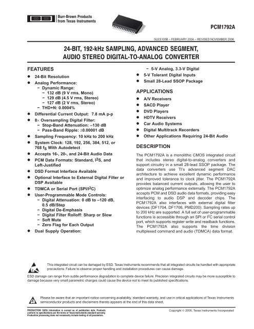
24-Bit, 192-kHz Sampling, Advanced Segment, Audio Stereo DAC ...
24-Bit, 192-kHz Sampling, Advanced Segment, Audio Stereo DAC ...
24-Bit, 192-kHz Sampling, Advanced Segment, Audio Stereo DAC ...

Create successful ePaper yourself
Turn your PDF publications into a flip-book with our unique Google optimized e-Paper software.
FEATURES<br />
<br />
<br />
<br />
SLES105B − FEBRUARY 2004 − REVISED NOVEMBER 2006<br />
<br />
<br />
<strong>24</strong>-<strong>Bit</strong> Resolution<br />
Analog Performance:<br />
− Dynamic Range:<br />
− 132 dB (9 V rms, Mono)<br />
− 129 dB (4.5 V rms, <strong>Stereo</strong>)<br />
− 127 dB (2 V rms, <strong>Stereo</strong>)<br />
− THD+N: 0.0004%<br />
Differential Current Output: 7.8 mA p-p<br />
8× Oversampling Digital Filter:<br />
− Stop-Band Attenuation: –130 dB<br />
− Pass-Band Ripple: ±0.00001 dB<br />
<strong>Sampling</strong> Frequency: 10 <strong>kHz</strong> to 200 <strong>kHz</strong><br />
System Clock: 128, <strong>192</strong>, 256, 384, 512, or<br />
768 f S With Autodetect<br />
Accepts 16-, 20-, and <strong>24</strong>-<strong>Bit</strong> <strong>Audio</strong> Data<br />
PCM Data Formats: Standard, I 2S, and<br />
Left-Justified<br />
DSD Format Interface Available<br />
Optional Interface to External Digital Filter or<br />
DSP Available<br />
TDMCA or Serial Port (SPI/I 2C)<br />
User-Programmable Mode Controls:<br />
− Digital Attenuation: 0 dB to –120 dB,<br />
0.5 dB/Step<br />
− Digital De-Emphasis<br />
− Digital Filter Rolloff: Sharp or Slow<br />
− Soft Mute<br />
− Zero Flag for Each Output<br />
Dual Supply Operation:<br />
− 5-V Analog, 3.3-V Digital<br />
5-V Tolerant Digital Inputs<br />
Small 28-Lead SSOP Package<br />
APPLICATIONS<br />
A/V Receivers<br />
SACD Player<br />
DVD Players<br />
HDTV Receivers<br />
Car <strong>Audio</strong> Systems<br />
Digital Multitrack Recorders<br />
Other Applications Requiring <strong>24</strong>-<strong>Bit</strong> <strong>Audio</strong><br />
DESCRIPTION<br />
The PCM1792A is a monolithic CMOS integrated circuit<br />
that includes stereo digital-to-analog converters and<br />
support circuitry in a small 28-lead SSOP package. The<br />
data converters use TI’s advanced segment <strong>DAC</strong><br />
architecture to achieve excellent dynamic performance<br />
and improved tolerance to clock jitter. The PCM1792A<br />
provides balanced current outputs, allowing the user to<br />
optimize analog performance externally. The PCM1792A<br />
accepts PCM and DSD audio data formats, providing easy<br />
interfacing to audio DSP and decoder chips. The<br />
PCM1792A also interfaces with external digital filter<br />
devices (DF1704, DF1706, PMD200). <strong>Sampling</strong> rates up<br />
to 200 <strong>kHz</strong> are supported. A full set of user-programmable<br />
functions is accessible through an SPI or I 2 C serial control<br />
port, which supports register write and readback functions.<br />
The PCM1792A also supports the time division<br />
multiplexed command and audio (TDMCA) data format.<br />
This integrated circuit can be damaged by ESD. Texas Instruments recommends that all integrated circuits be handled with appropriate<br />
precautions. Failure to observe proper handling and installation procedures can cause damage.<br />
ESD damage can range from subtle performance degradation to complete device failure. Precision integrated circuits may be more susceptible to<br />
damage because very small parametric changes could cause the device not to meet its published specifications.<br />
Please be aware that an important notice concerning availability, standard warranty, and use in critical applications of Texas Instruments<br />
semiconductor products and disclaimers thereto appears at the end of this data sheet.<br />
<br />
<br />
<br />
Copyright © 2006, Texas Instruments Incorporated
SLES105B − FEBRUARY 2004 − REVISED NOVEMBER 2006<br />
ORDERING INFORMATION<br />
2<br />
PRODUCT PACKAGE PACKAGE CODE<br />
OPERATION<br />
TEMPERATURE<br />
RANGE<br />
PACKAGE<br />
MARKING<br />
PCM1792ADB 28-lead SSOP 28DB −25°C to 85°C PCM1792A<br />
ABSOLUTE MAXIMUM RATINGS<br />
over operating free-air temperature range unless otherwise noted(1)<br />
ORDERING<br />
NUMBER<br />
www.ti.com<br />
TRANSPORT<br />
MEDIA<br />
PCM1792ADB Tube<br />
PCM1792ADBR Tape and reel<br />
PCM1792A<br />
Supply voltage<br />
VCC1, VCC2L, VCC2R<br />
VDD<br />
−0.3 V to 6.5 V<br />
−0.3 V to 4 V<br />
Supply voltage differences: VCC1, VCC2L and VCC2R ±0.1 V<br />
Ground voltage differences: AGND1, AGND2, AGND3L, AGND3R, and DGND ±0.1 V<br />
Digital input LRCK, DATA, BCK, SCK, MSEL, RST, MS(2), MDI, MC, MDO(2), ZEROL(2), ZEROR(2) –0.3 V to 6.5 V<br />
voltage ZEROL(3), ZEROR(3), MDO(3), MS(3) –0.3 V to (VDD + 0.3 V) < 4 V<br />
Analog input voltage –0.3 V to (VCC + 0.3 V) < 6.5 V<br />
Input current (any pins except supplies) ±10 mA<br />
Ambient temperature under bias –40°C to 125°C<br />
Storage temperature –55°C to 150°C<br />
Junction temperature 150°C<br />
Lead temperature (soldering) 260°C, 5 s<br />
Package temperature (IR reflow, peak) 250°C<br />
(1) Stresses beyond those listed under “absolute maximum ratings” may cause permanent damage to the device. These are stress ratings only, and<br />
functional operation of the device at these or any other conditions beyond those indicated under “recommended operating conditions” is not<br />
implied. Exposure to absolute-maximum-rated conditions for extended periods may affect device reliability.<br />
(2) Input mode or I2C mode.<br />
(3) Output mode except for I2C mode.<br />
ELECTRICAL CHARACTERISTICS<br />
all specifications at TA = 25°C, VCC1 = VCC2L = VCC2R = 5 V, fS = 44.1 <strong>kHz</strong>, system clock = 256 fS, and <strong>24</strong>-bit data unless otherwise noted<br />
PARAMETER TEST CONDITIONS<br />
PCM1792ADB<br />
MIN TYP MAX<br />
RESOLUTION <strong>24</strong> <strong>Bit</strong>s<br />
DATA FORMAT (PCM Mode)<br />
<strong>Audio</strong> data interface format Standard, I2S, left justified<br />
<strong>Audio</strong> data bit length 16-, 20-, <strong>24</strong>-bit selectable<br />
<strong>Audio</strong> data format MSB first, 2s complement<br />
fS <strong>Sampling</strong> frequency 10 200 <strong>kHz</strong><br />
System clock frequency 128, <strong>192</strong>, 256, 384, 512, 768 fS<br />
DATA FORMAT (DSD Mode)<br />
<strong>Audio</strong> data interface format DSD (direct stream digital)<br />
<strong>Audio</strong> data bit length 1 <strong>Bit</strong><br />
fS <strong>Sampling</strong> frequency 2.82<strong>24</strong> MHz<br />
System clock frequency 2.82<strong>24</strong> 11.2896 MHz<br />
DIGITAL INPUT/OUTPUT<br />
Logic family TTL compatible<br />
VIH<br />
VIL<br />
Input logic level<br />
IIH<br />
IIL<br />
Input logic current<br />
VOH<br />
VOL<br />
Output logic level<br />
VIN = VDD<br />
10<br />
VIN = 0 V –10<br />
IOH = −2 mA 2.4<br />
IOL = 2 mA 0.4<br />
2<br />
0.8<br />
UNIT<br />
Vdc<br />
µA<br />
Vdc
www.ti.com<br />
<br />
SLES105B − FEBRUARY 2004 − REVISED NOVEMBER 2006<br />
ELECTRICAL CHARACTERISTICS (Continued)<br />
all specifications at TA = 25°C, VCC1 = VCC2L = VCC2R = 5 V, fS = 44.1 <strong>kHz</strong>, system clock = 256 fS, and <strong>24</strong>-bit data unless otherwise noted<br />
PARAMETER TEST CONDITIONS<br />
DYNAMIC PERFORMANCE (PCM MODE, 2-V RMS OUTPUT) (1)(2)<br />
PCM1792ADB<br />
MIN TYP MAX<br />
fS = 44.1 <strong>kHz</strong> 0.0004% 0.0008%<br />
THD+N at VOUT VOUT = 0 dB<br />
fS = 96 <strong>kHz</strong> 0.0008%<br />
fS = <strong>192</strong> <strong>kHz</strong> 0.0015%<br />
EIAJ, A-weighted, fS = 44.1 <strong>kHz</strong> 123 127<br />
Dynamic range<br />
EIAJ, A-weighted, fS = 96 <strong>kHz</strong> 127 dB<br />
EIAJ, A-weighted, fS = <strong>192</strong> <strong>kHz</strong> 127<br />
EIAJ, A-weighted, fS = 44.1 <strong>kHz</strong> 123 127<br />
Signal-to-noise ratio<br />
EIAJ, A-weighted, fS = 96 <strong>kHz</strong> 127 dB<br />
EIAJ, A-weighted, fS = <strong>192</strong> <strong>kHz</strong> 127<br />
fS = 44.1 <strong>kHz</strong> 120 123<br />
Channel separation<br />
fS = 96 <strong>kHz</strong> 122 dB<br />
fS = <strong>192</strong> <strong>kHz</strong> 120<br />
Level Linearity Error VOUT = −120 dB ±1 dB<br />
DYNAMIC PERFORMANCE (PCM Mode, 4.5-V RMS Output) (1)(3)<br />
fS = 44.1 <strong>kHz</strong> 0.0004%<br />
THD+N at VOUT VOUT = 0 dB<br />
fS = 96 <strong>kHz</strong> 0.0008%<br />
fS = <strong>192</strong> <strong>kHz</strong> 0.0015%<br />
EIAJ, A-weighted, fS = 44.1 <strong>kHz</strong> 129<br />
Dynamic range<br />
EIAJ, A-weighted, fS = 96 <strong>kHz</strong> 129 dB<br />
EIAJ, A-weighted, fS = <strong>192</strong> <strong>kHz</strong> 129<br />
EIAJ, A-weighted, fS = 44.1 <strong>kHz</strong> 129<br />
Signal-to-noise ratio<br />
EIAJ, A-weighted, fS = 96 <strong>kHz</strong> 129 dB<br />
EIAJ, A-weighted, fS = <strong>192</strong> <strong>kHz</strong> 129<br />
fS = 44.1 <strong>kHz</strong> 1<strong>24</strong><br />
Channel separation<br />
fS = 96 <strong>kHz</strong> 123 dB<br />
DYNAMIC PERFORMANCE (MONO MODE) (1)(3)<br />
fS = <strong>192</strong> <strong>kHz</strong> 121<br />
fS = 44.1 <strong>kHz</strong> 0.0004%<br />
THD+N at VOUT VOUT = 0 dB<br />
fS = 96 <strong>kHz</strong> 0.0008%<br />
fS = <strong>192</strong> <strong>kHz</strong> 0.0015%<br />
EIAJ, A-weighted, fS = 44.1 <strong>kHz</strong> 132<br />
Dynamic range<br />
EIAJ, A-weighted, fS = 96 <strong>kHz</strong> 132 dB<br />
EIAJ, A-weighted, fS = <strong>192</strong> <strong>kHz</strong> 132<br />
EIAJ, A-weighted, fS = 44.1 <strong>kHz</strong> 132<br />
Signal-to-noise ratio<br />
EIAJ, A-weighted, fS = 96 <strong>kHz</strong> 132 dB<br />
EIAJ, A-weighted, fS = <strong>192</strong> <strong>kHz</strong> 132<br />
(1) Filter condition:<br />
THD+N: 20-Hz HPF, 20-<strong>kHz</strong> apogee LPF<br />
Dynamic range: 20-Hz HPF, 20-<strong>kHz</strong> AES17 LPF, A-weighted<br />
Signal-to-noise ratio: 20-Hz HPF, 20-<strong>kHz</strong> AES17 LPF, A-weighted<br />
Channel separation: 20-Hz HPF, 20-<strong>kHz</strong> AES17 LPF<br />
Analog performance specifications are measured using the System Two Cascade audio measurement system by <strong>Audio</strong> Precision in the<br />
averaging mode.<br />
(2) Dynamic performance and dc accuracy are specified at the output of the postamplifier as shown in Figure 36.<br />
(3) Dynamic performance and dc accuracy are specified at the output of the postamplifier as shown in Figure 37.<br />
<strong>Audio</strong> Precision and System Two are trademarks of <strong>Audio</strong> Precision, Inc.<br />
Other trademarks are the property of their respective owners.<br />
UNIT<br />
3
SLES105B − FEBRUARY 2004 − REVISED NOVEMBER 2006<br />
4<br />
www.ti.com<br />
ELECTRICAL CHARACTERISTICS (Continued)<br />
all specifications at TA = 25°C, VCC1 = VCC2L = VCC2R = 5 V, fS = 44.1 <strong>kHz</strong>, system clock = 256 fS, and <strong>24</strong>-bit data unless otherwise noted<br />
PARAMETER TEST CONDITIONS<br />
DSD MODE DYNAMIC PERFORMANCE (1) (2) (44.1 <strong>kHz</strong>, 64 fS)<br />
PCM1792ADB<br />
MIN TYP MAX<br />
THD+N at FS 4.5 V rms 0.0005%<br />
Dynamic range –60 dB, EIAJ, A-weighted 128 dB<br />
Signal-to-noise ratio EIAJ, A-weighted 128 dB<br />
ANALOG OUTPUT<br />
Gain error –6 ±2 6 % of FSR<br />
Gain mismatch, channel-to-channel –3 ±0.5 3 % of FSR<br />
Bipolar zero error At BPZ –2 ±0.5 2 % of FSR<br />
Output current Full scale (0 dB) 7.8 mA p-p<br />
Center current At BPZ –6.2 mA<br />
DIGITAL FILTER PERFORMANCE<br />
De-emphasis error ±0.004 dB<br />
FILTER CHARACTERISTICS–1: SHARP ROLLOFF<br />
Pass band<br />
±0.00001 dB 0.454 fS<br />
–3 dB 0.49 fS<br />
Stop band 0.546 fS<br />
Pass-band ripple ±0.00001 dB<br />
Stop-band attenuation Stop band = 0.546 fS –130 dB<br />
Delay time 55/fS s<br />
FILTER CHARACTERISTICS–2: SLOW ROLLOFF<br />
Pass band<br />
±0.04 dB 0.254 fS<br />
–3 dB 0.46 fS<br />
Stop band 0.732 fS<br />
Pass-band ripple ±0.001 dB<br />
Stop-band attenuation Stop band = 0.732 fS –100 dB<br />
Delay time<br />
(1) Filter condition:<br />
THD+N: 20-Hz HPF, 20-<strong>kHz</strong> apogee LPF<br />
Dynamic range: 20-Hz HPF, 20-<strong>kHz</strong> AES17 LPF, A-weighted<br />
Signal-to-noise ratio: 20-Hz HPF, 20-<strong>kHz</strong> AES17 LPF, A-weighted<br />
Channel separation: 20-Hz HPF, 20-<strong>kHz</strong> AES17 LPF<br />
18/fS s<br />
Analog performance specifications are measured using the System Two Cascade audio measurement system by <strong>Audio</strong> Precision in the averaging<br />
mode.<br />
(2) Dynamic performance and dc accuracy are specified at the output of the postamplifier as shown in Figure 38.<br />
UNIT
www.ti.com<br />
<br />
SLES105B − FEBRUARY 2004 − REVISED NOVEMBER 2006<br />
ELECTRICAL CHARACTERISTICS (Continued)<br />
all specifications at TA = 25°C, VCC1 = VCC2L = VCC2R = 5 V, fS = 44.1 <strong>kHz</strong>, system clock = 256 fS, and <strong>24</strong>-bit data unless otherwise noted<br />
POWER SUPPLY REQUIREMENTS<br />
PARAMETER TEST CONDITIONS<br />
PCM1792ADB<br />
MIN TYP MAX<br />
VDD 3 3.3 3.6 Vdc<br />
VCC1<br />
VCC2L<br />
VCC2R<br />
Voltage range<br />
UNIT<br />
4.75 5 5.25 Vdc<br />
fS = 44.1 <strong>kHz</strong> 12 15<br />
IDD IDD Supply current (1)<br />
(1) fS = 96 <strong>kHz</strong> 23 mA<br />
fS = <strong>192</strong> <strong>kHz</strong> 45<br />
fS = 44.1 <strong>kHz</strong> 33 40<br />
ICC ICC Supply current (1)<br />
(1) fS = 96 <strong>kHz</strong> 35 mA<br />
fS = <strong>192</strong> <strong>kHz</strong> 37<br />
fS = 44.1 <strong>kHz</strong> 205 250<br />
Power dissipation (1)<br />
fS = 96 <strong>kHz</strong> 250 mW<br />
TEMPERATURE RANGE<br />
fS = <strong>192</strong> <strong>kHz</strong> 335<br />
Operation temperature –25 85 °C<br />
θJA Thermal resistance 28-pin SSOP 100 °C/W<br />
(1) Input is BPZ data.<br />
PIN ASSIGNMENTS<br />
ZEROL<br />
ZEROR<br />
MSEL<br />
LRCK<br />
DATA<br />
BCK<br />
SCK<br />
DGND<br />
V DD<br />
MS<br />
MDI<br />
MC<br />
MDO<br />
RST<br />
1<br />
2<br />
3<br />
4<br />
5<br />
6<br />
7<br />
8<br />
9<br />
10<br />
11<br />
12<br />
13<br />
14<br />
PCM1792A<br />
(TOP VIEW)<br />
28<br />
27<br />
26<br />
25<br />
<strong>24</strong><br />
23<br />
22<br />
21<br />
20<br />
19<br />
18<br />
17<br />
16<br />
15<br />
V CC 2L<br />
AGND3L<br />
I OUT L−<br />
I OUT L+<br />
AGND2<br />
V CC 1<br />
V COM L<br />
V COM R<br />
I REF<br />
AGND1<br />
I OUT R−<br />
I OUT R+<br />
AGND3R<br />
V CC 2R<br />
5
SLES105B − FEBRUARY 2004 − REVISED NOVEMBER 2006<br />
6<br />
TERMINAL<br />
NAME PIN<br />
Terminal Functions<br />
I/O DESCRIPTIONS<br />
AGND1 19 − Analog ground (internal bias)<br />
AGND2 <strong>24</strong> − Analog ground (internal bias)<br />
AGND3L 27 − Analog ground (L-channel <strong>DAC</strong>FF)<br />
AGND3R 16 − Analog ground (R-channel <strong>DAC</strong>FF)<br />
BCK 6 I <strong>Bit</strong> clock input(1)<br />
DATA 5 I Serial audio data input for normal operation(1)<br />
DGND 8 − Digital ground<br />
IOUTL+ 25 O L-channel analog current output+<br />
IOUTL– 26 O L-channel analog current output–<br />
IOUTR+ 17 O R-channel analog current output+<br />
IOUTR– 18 O R-channel analog current output–<br />
IREF 20 − Output current reference bias pin<br />
LRCK 4 I Left and right clock (fS) input for normal operation(1)<br />
MC 12 I Mode control clock input(1)<br />
MDI 11 I Mode control data input(1)<br />
MDO 13 I/O Mode control readback data output(3)<br />
MS 10 I/O Mode control chip-select input(2)<br />
MSEL 3 I I2C/SPI select(1)<br />
RST 14 I Reset(1)<br />
SCK 7 I System clock input(1)<br />
VCC1 23 − Analog power supply, 5 V<br />
VCC2L 28 − Analog power supply (L-channel <strong>DAC</strong>FF), 5 V<br />
VCC2R 15 − Analog power supply (R-channel <strong>DAC</strong>FF), 5 V<br />
VCOML 22 − L-channel internal bias decoupling pin<br />
VCOMR 21 − R-channel internal bias decoupling pin<br />
VDD 9 − Digital power supply, 3.3 V<br />
ZEROL 1 I/O Zero flag for L-channel(2)<br />
www.ti.com<br />
ZEROR 2 I/O Zero flag for R-channel(2)<br />
(1) Schmitt-trigger input, 5-V tolerant<br />
(2) Schmitt-trigger input and output. 5-V tolerant input and CMOS output<br />
(3) Schmitt-trigger input and output. 5-V tolerant input. In I2C mode, this pin becomes an open-drain 3-state output; otherwise, this pin is a CMOS<br />
output.
www.ti.com<br />
FUNCTIONAL BLOCK DIAGRAM<br />
LRCK<br />
BCK<br />
DATA<br />
RST<br />
MDO<br />
MDI<br />
MC<br />
MS<br />
MSEL<br />
ZEROL<br />
ZEROR<br />
<strong>Audio</strong><br />
Data Input<br />
I/F<br />
Function<br />
Control<br />
I/F<br />
Zero<br />
Detect<br />
8<br />
Oversampling<br />
Digital<br />
Filter<br />
and<br />
Function<br />
Control<br />
System<br />
Clock<br />
Manager<br />
SCK<br />
<strong>Advanced</strong><br />
<strong>Segment</strong><br />
<strong>DAC</strong><br />
Modulator<br />
DGND<br />
VDD<br />
AGND1<br />
Bias<br />
and<br />
Vref<br />
Current<br />
<strong>Segment</strong><br />
<strong>DAC</strong><br />
Power Supply<br />
AGND2<br />
AGND3L<br />
Current<br />
<strong>Segment</strong><br />
<strong>DAC</strong><br />
AGND3R<br />
<br />
SLES105B − FEBRUARY 2004 − REVISED NOVEMBER 2006<br />
VCC1<br />
VCC2L<br />
IOUTL−<br />
IOUTL+<br />
VCOML<br />
IREF<br />
VCOMR<br />
IOUTR−<br />
IOUTR+<br />
VCC2R<br />
I/V and Filter<br />
I/V and Filter<br />
VOUTL<br />
VOUTR<br />
7
SLES105B − FEBRUARY 2004 − REVISED NOVEMBER 2006<br />
DIGITAL FILTER<br />
Digital Filter Response<br />
Amplitude − dB<br />
Amplitude − dB<br />
8<br />
0<br />
−50<br />
−100<br />
−150<br />
AMPLITUDE<br />
vs<br />
FREQUENCY<br />
−200<br />
0 1 2 3 4<br />
Frequency [× fS]<br />
Figure 1. Frequency Response, Sharp Rolloff<br />
0<br />
−50<br />
−100<br />
−150<br />
AMPLITUDE<br />
vs<br />
FREQUENCY<br />
−200<br />
0 1 2 3 4<br />
Frequency [× fS]<br />
Figure 3. Frequency Response, Slow Rolloff<br />
TYPICAL PERFORMANCE CURVES<br />
Amplitude − dB<br />
0.00002 2<br />
0.00001 1<br />
0<br />
−0.00001 −1<br />
AMPLITUDE<br />
vs<br />
FREQUENCY<br />
www.ti.com<br />
−0.00002 −2<br />
0.0 0.1 0.2 0.3 0.4 0.5<br />
Frequency [× fS]<br />
Amplitude − dB<br />
Figure 2. Pass-Band Ripple, Sharp Rolloff<br />
0<br />
−2<br />
−4<br />
−6<br />
−8<br />
−10<br />
−12<br />
−14<br />
−16<br />
−18<br />
AMPLITUDE<br />
vs<br />
FREQUENCY<br />
−20<br />
0.0 0.1 0.2 0.3 0.4 0.5 0.6<br />
Frequency [× fS]<br />
Figure 4. Transition Characteristics, Slow Rolloff
www.ti.com<br />
De-Emphasis Filter<br />
De-Emphasis Level − dB<br />
De-Emphasis Level − dB<br />
0<br />
−2<br />
−4<br />
−6<br />
−8<br />
DE-EMPHASIS LEVEL<br />
vs<br />
FREQUENCY<br />
−10<br />
0 2 4 6 8 10 12 14<br />
0<br />
−2<br />
−4<br />
−6<br />
−8<br />
f − Frequency − <strong>kHz</strong><br />
Figure 5<br />
DE-EMPHASIS LEVEL<br />
vs<br />
FREQUENCY<br />
f − Frequency − <strong>kHz</strong><br />
Figure 7<br />
fS = 32 <strong>kHz</strong><br />
fS = 44.1 <strong>kHz</strong><br />
−10<br />
0 2 4 6 8 10 12 14 16 18 20<br />
De-Emphasis Error − dB<br />
De-Emphasis Error − dB<br />
20<br />
0.015 15<br />
0.010 10<br />
0.005 5<br />
0<br />
−0.005 −5<br />
−0.010 −10<br />
−0.015 −15<br />
<br />
SLES105B − FEBRUARY 2004 − REVISED NOVEMBER 2006<br />
fS = 32 <strong>kHz</strong><br />
DE-EMPHASIS ERROR<br />
vs<br />
FREQUENCY<br />
−0.020 −20<br />
0 2 4 6 8 10 12 14<br />
0.020 20<br />
0.015 15<br />
0.010 10<br />
0.005 5<br />
0<br />
−0.005 −5<br />
−0.010 −10<br />
−0.015 −15<br />
fS = 44.1 <strong>kHz</strong><br />
f − Frequency − <strong>kHz</strong><br />
Figure 6<br />
DE-EMPHASIS ERROR<br />
vs<br />
FREQUENCY<br />
−0.020 −20<br />
0 2 4 6 8 10 12 14 16 18 20<br />
f − Frequency − <strong>kHz</strong><br />
Figure 8<br />
9
SLES105B − FEBRUARY 2004 − REVISED NOVEMBER 2006<br />
De-Emphasis Filter (Continued)<br />
De-Emphasis Level − dB<br />
10<br />
0<br />
−2<br />
−4<br />
−6<br />
−8<br />
DE-EMPHASIS LEVEL<br />
vs<br />
FREQUENCY<br />
−10<br />
0 2 4 6 8 10 12 14 16 18 20 22<br />
f − Frequency − <strong>kHz</strong><br />
Figure 9<br />
fS = 48 <strong>kHz</strong><br />
De-Emphasis Error − dB<br />
0.020 20<br />
0.015 15<br />
0.010 10<br />
0.005 5<br />
0<br />
−0.005 −5<br />
−0.010 −10<br />
−0.015 −15<br />
fS = 48 <strong>kHz</strong><br />
DE-EMPHASIS ERROR<br />
vs<br />
FREQUENCY<br />
f − Frequency − <strong>kHz</strong><br />
Figure 10<br />
www.ti.com<br />
−0.020 −20<br />
0 2 4 6 8 10 12 14 16 18 20 22
www.ti.com<br />
ANALOG DYNAMIC PERFORMANCE<br />
Supply Voltage Characteristics<br />
THD+N − Total Harmonic Distortion + Noise − %<br />
SNR − Signal-to-Noise Ratio − dB<br />
0.01<br />
0.001<br />
TOTAL HARMONIC DISTORTION + NOISE<br />
vs<br />
SUPPLY VOLTAGE<br />
fS = <strong>192</strong> <strong>kHz</strong><br />
0.0001<br />
4.50 4.75 5.00 5.25 5.50<br />
132<br />
130<br />
128<br />
126<br />
1<strong>24</strong><br />
fS = 48 <strong>kHz</strong><br />
VCC − Supply Voltage − V<br />
Figure 11<br />
fS = 96 <strong>kHz</strong><br />
SIGNAL-to-NOISE RATIO<br />
vs<br />
SUPPLY VOLTAGE<br />
fS = 48 <strong>kHz</strong><br />
fS = 96 <strong>kHz</strong><br />
Figure 13<br />
fS = <strong>192</strong> <strong>kHz</strong><br />
122<br />
4.50 4.75 5.00 5.25 5.50<br />
VCC − Supply Voltage − V<br />
Dynamic Range − dB<br />
Channel Separation − dB<br />
132<br />
130<br />
128<br />
126<br />
1<strong>24</strong><br />
<br />
SLES105B − FEBRUARY 2004 − REVISED NOVEMBER 2006<br />
fS = 96 <strong>kHz</strong><br />
DYNAMIC RANGE<br />
vs<br />
SUPPLY VOLTAGE<br />
fS = <strong>192</strong> <strong>kHz</strong><br />
122<br />
4.50 4.75 5.00 5.25 5.50<br />
130<br />
128<br />
126<br />
1<strong>24</strong><br />
122<br />
VCC − Supply Voltage − V<br />
Figure 12<br />
VCC − Supply Voltage − V<br />
Figure 14<br />
fS = 48 <strong>kHz</strong><br />
CHANNEL SEPARATION<br />
vs<br />
SUPPLY VOLTAGE<br />
fS = <strong>192</strong> <strong>kHz</strong><br />
NOTE: PCM mode, TA = 25°C, VDD = 3.3 V, measurement circuit is Figure 37 (VOUT = 4.5 V rms).<br />
fS = 96 <strong>kHz</strong><br />
fS = 48 <strong>kHz</strong><br />
120<br />
4.50 4.75 5.00 5.25 5.50<br />
11
SLES105B − FEBRUARY 2004 − REVISED NOVEMBER 2006<br />
Temperature Characteristics<br />
THD+N − Total Harmonic Distortion + Noise − %<br />
SNR − Signal-to-Noise Ratio − dB<br />
12<br />
0.01<br />
0.001<br />
TOTAL HARMONIC DISTORTION + NOISE<br />
vs<br />
FREE-AIR TEMPERATURE<br />
fS = <strong>192</strong> <strong>kHz</strong><br />
0.0001<br />
−50 −25 0 25 50 75 100<br />
132<br />
130<br />
128<br />
126<br />
1<strong>24</strong><br />
TA − Free-Air Temperature − °C<br />
Figure 15<br />
fS = 96 <strong>kHz</strong><br />
SIGNAL-to-NOISE RATIO<br />
vs<br />
FREE-AIR TEMPERATURE<br />
fS = 96 <strong>kHz</strong><br />
fS = <strong>192</strong> <strong>kHz</strong><br />
fS = 48 <strong>kHz</strong><br />
fS = 48 <strong>kHz</strong><br />
122<br />
−50 −25 0 25 50 75 100<br />
TA − Free-Air Temperature − °C<br />
Figure 17<br />
NOTE: PCM mode, VDD = 3.3 V, VCC = 5 V, measurement circuit is Figure 37 (VOUT = 4.5 V rms).<br />
Dynamic Range − dB<br />
Channel Separation − dB<br />
132<br />
130<br />
128<br />
126<br />
1<strong>24</strong><br />
DYNAMIC RANGE<br />
vs<br />
FREE-AIR TEMPERATURE<br />
fS = 96 <strong>kHz</strong><br />
fS = 48 <strong>kHz</strong><br />
TA − Free-Air Temperature − °C<br />
Figure 16<br />
fS = <strong>192</strong> <strong>kHz</strong><br />
www.ti.com<br />
122<br />
−50 −25 0 25 50 75 100<br />
130<br />
128<br />
126<br />
1<strong>24</strong><br />
122<br />
CHANNEL SEPARATION<br />
vs<br />
FREE-AIR TEMPERATURE<br />
fS = <strong>192</strong> <strong>kHz</strong><br />
120<br />
−50 −25 0 25 50 75 100<br />
TA − Free-Air Temperature − °C<br />
Figure 18<br />
fS = 96 <strong>kHz</strong><br />
fS = 48 <strong>kHz</strong>
Amplitude − dB<br />
www.ti.com<br />
0<br />
−20<br />
−40<br />
−60<br />
−80<br />
−100<br />
−120<br />
−140<br />
−160<br />
AMPLITUDE<br />
vs<br />
FREQUENCY<br />
−180<br />
0 2 4 6 8 10 12 14 16 18 20<br />
f − Frequency − <strong>kHz</strong><br />
<br />
SLES105B − FEBRUARY 2004 − REVISED NOVEMBER 2006<br />
−160<br />
0 10 20 30 40 50 60 70 80 90 100<br />
f − Frequency − <strong>kHz</strong><br />
Figure 19. −60-dB Output Spectrum, BW = 20 <strong>kHz</strong> Figure 20. −60-dB Output Spectrum, BW = 100 <strong>kHz</strong><br />
NOTE: PCM mode, fS = 48 <strong>kHz</strong>, 32,768 point 8 average, TA = 25°C, VDD = 3.5 V VCC = 5 V, measurement circuit is Figure 37.<br />
THD+N − Total Harmonic Distortion + Noise − %<br />
10<br />
1<br />
0.1<br />
0.01<br />
0.001<br />
Amplitude − dB<br />
0<br />
−20<br />
−40<br />
−60<br />
−80<br />
−100<br />
−120<br />
−140<br />
TOTAL HARMONIC DISTORTION + NOISE<br />
vs<br />
INPUT LEVEL<br />
0.0001<br />
−100 −80 −60 −40 −20 0<br />
Input Level − dBFS<br />
Figure 21. THD+N vs Input Level, PCM Mode<br />
AMPLITUDE<br />
vs<br />
FREQUENCY<br />
NOTE: PCM mode, fS = 48 <strong>kHz</strong>, TA = 25°C, VDD = 3.3 V, VCC = 5 V, measurement circuit is Figure 37.<br />
13
SLES105B − FEBRUARY 2004 − REVISED NOVEMBER 2006<br />
14<br />
Amplitude − dB<br />
0<br />
−20<br />
−40<br />
−60<br />
−80<br />
−100<br />
−120<br />
−140<br />
AMPLITUDE<br />
vs<br />
FREQUENCY<br />
−160<br />
0 2 4 6 8 10 12 14 16 18 20<br />
f − Frequency − <strong>kHz</strong><br />
Figure 22. −60-dB Output Spectrum, DSD Mode<br />
www.ti.com<br />
NOTE: DSD mode (FIR-4), 32,768 point 8 average, TA = 25°C, VDD = 3.3 V, VCC = 5 V, measurement circuit is Figure 38.<br />
Amplitude − dB<br />
−130<br />
−133<br />
−136<br />
−139<br />
−142<br />
−145<br />
−148<br />
−151<br />
−154<br />
−157<br />
AMPLITUDE<br />
vs<br />
FREQUENCY<br />
−160<br />
0 2 4 6 8 10 12 14 16 18 20<br />
f − Frequency − <strong>kHz</strong><br />
Figure 23. −150-dB Output Spectrum, DSD Mono Mode<br />
NOTE: DSD mode (FIR-4), 32,768 point 8 average, TA = 25°C, VDD = 3.3 V, VCC = 5 V, measurement circuit is Figure 38.
www.ti.com<br />
SYSTEM CLOCK AND RESET FUNCTIONS<br />
System Clock Input<br />
<br />
SLES105B − FEBRUARY 2004 − REVISED NOVEMBER 2006<br />
The PCM1792A requires a system clock for operating the digital interpolation filters and advanced segment <strong>DAC</strong><br />
modulators. The system clock is applied at the SCK input (pin 7). The PCM1792A has a system clock detection circuit that<br />
automatically senses if the system clock is operating between 128 fS and 768 fS. Table 1 shows examples of system clock<br />
frequencies for common audio sampling rates. If the oversampling rate of the delta-sigma modulator is selected as 128 fS,<br />
the system clock frequency is over 256 fS.<br />
Figure <strong>24</strong> shows the timing requirements for the system clock input. For optimal performance, it is important to use a clock<br />
source with low phase jitter and noise. One of the Texas Instruments’ PLL1700 family of multiclock generators is an<br />
excellent choice for providing the PCM1792A system clock.<br />
Table 1. System Clock Rates for Common <strong>Audio</strong> <strong>Sampling</strong> Frequencies<br />
SAMPLING FREQUENCY<br />
128 fS<br />
SYSTEM CLOCK FREQUENCY (fSCK) (MHz)<br />
<strong>192</strong> fS 256 fS 384 fS 512 fS 768 fS<br />
32 <strong>kHz</strong> 4.096(1) 6.144(1) 8.<strong>192</strong> 12.288 16.384 <strong>24</strong>.576<br />
44.1 <strong>kHz</strong> 5.6488(1) 8.4672 11.2896 16.9344 22.5792 33.8688<br />
48 <strong>kHz</strong> 6.144(1) 9.216 12.288 18.432 <strong>24</strong>.576 36.864<br />
96 <strong>kHz</strong> 12.288 18.432 <strong>24</strong>.576 36.864 49.152(1) 73.728(1)<br />
<strong>192</strong> <strong>kHz</strong> <strong>24</strong>.576 36.864 49.152(1) 73.728(1) (2) (2)<br />
(1) This system clock rate is not supported in I2C fast mode.<br />
(2) This system clock rate is not supported for the given sampling frequency.<br />
System Clock (SCK)<br />
H<br />
L<br />
t(SCKL)<br />
t(SCKH)<br />
t(SCY)<br />
PARAMETERS MIN MAX UNITS<br />
t(SCY) System clock pulse cycle time 13 ns<br />
t(SCKH) System clock pulse duration, HIGH 0.4 t(SCY) ns<br />
t(SCKL) System clock pulse duration, LOW 0.4 t(SCY) ns<br />
Power-On and External Reset Functions<br />
Figure <strong>24</strong>. System Clock Input Timing<br />
The PCM1792A includes a power-on reset function. Figure 25 shows the operation of this function. With VDD > 2 V, the<br />
power-on reset function is enabled. The initialization sequence requires 10<strong>24</strong> system clocks from the time VDD > 2 V. After<br />
the initialization period, the PCM1792A is set to its default reset state, as described in the MODE CONTROL REGISTERS<br />
section of this data sheet.<br />
The PCM1792A also includes an external reset capability using the RST input (pin 14). This allows an external controller<br />
or master reset circuit to force the PCM1792A to initialize to its default reset state.<br />
Figure 26 shows the external reset operation and timing. The RST pin is set to logic 0 for a minimum of 20 ns. The RST<br />
pin is then set to a logic 1 state, thus starting the initialization sequence, which requires 10<strong>24</strong> system clock periods. The<br />
external reset is especially useful in applications where there is a delay between the PCM1792A power up and system clock<br />
activation.<br />
2 V<br />
0.8 V<br />
15
SLES105B − FEBRUARY 2004 − REVISED NOVEMBER 2006<br />
16<br />
VDD<br />
2.4 V (Max)<br />
2 V (Typ)<br />
1.6 V (Min)<br />
Internal Reset<br />
System Clock<br />
RST (Pin 14)<br />
Internal Reset<br />
System Clock<br />
Reset Reset Removal<br />
10<strong>24</strong> System Clocks<br />
Figure 25. Power-On Reset Timing<br />
t(RST)<br />
Reset Reset Removal<br />
10<strong>24</strong> System Clocks<br />
50 % of VDD<br />
PARAMETERS MIN MAX UNITS<br />
t(RST) Reset pulse duration, LOW 20 ns<br />
Figure 26. External Reset Timing<br />
www.ti.com
www.ti.com<br />
AUDIO DATA INTERFACE<br />
<strong>Audio</strong> Serial Interface<br />
<br />
SLES105B − FEBRUARY 2004 − REVISED NOVEMBER 2006<br />
The audio interface port is a 3-wire serial port. It includes LRCK (pin 4), BCK (pin 6), and DATA (pin 5). BCK is the serial<br />
audio bit clock, and it is used to clock the serial data present on DATA into the serial shift register of the audio interface.<br />
Serial data is clocked into the PCM1792A on the rising edge of BCK. LRCK is the serial audio left/right word clock.<br />
The PCM1792A requires the synchronization of LRCK and system clock, but does not need a specific phase relation<br />
between LRCK and system clock.<br />
If the relationship between LRCK and system clock changes more than ±6 BCK, internal operation is initialized within 1/fS<br />
and analog outputs are forced to the bipolar zero level until resynchronization between LRCK and system clock is<br />
completed.<br />
PCM <strong>Audio</strong> Data Formats and Timing<br />
The PCM1792A supports industry-standard audio data formats, including standard right-justified, I 2 S, and left-justified. The<br />
data formats are shown in Figure 28. Data formats are selected using the format bits, FMT[2:0], in control register 18. The<br />
default data format is <strong>24</strong>-bit I 2 S. All formats require binary 2s complement, MSB-first audio data. Figure 27 shows a detailed<br />
timing diagram for the serial audio interface.<br />
LRCK<br />
BCK<br />
DATA<br />
t(BCH)<br />
t(BCY)<br />
t(DS)<br />
t(BCL)<br />
t(BL)<br />
t(DH)<br />
t(LB)<br />
PARAMETERS MIN MAX UNITS<br />
t(BCY) BCK pulse cycle time 70 ns<br />
t(BCL) BCK pulse duration, LOW 30 ns<br />
t(BCH) BCK pulse duration, HIGH 30 ns<br />
t(BL) BCK rising edge to LRCK edge 10 ns<br />
t(LB) LRCK edge to BCK rising edge 10 ns<br />
t(DS) DATA setup time 10 ns<br />
t(DH) DATA hold time 10 ns<br />
— LRCK clock duty 50% ± 2 bit clocks<br />
Figure 27. Timing of <strong>Audio</strong> Interface<br />
50% of VDD<br />
50% of VDD<br />
50% of VDD<br />
17
SLES105B − FEBRUARY 2004 − REVISED NOVEMBER 2006<br />
(1) Standard Data Format (Right-Justified); L-Channel = HIGH, R-Channel = LOW<br />
18<br />
LRCK<br />
BCK<br />
<strong>Audio</strong> Data Word = 16-<strong>Bit</strong><br />
DATA<br />
<strong>Audio</strong> Data Word = 20-<strong>Bit</strong><br />
DATA<br />
14 15 16 1 2 15 16<br />
18 19 20<br />
<strong>Audio</strong> Data Word = <strong>24</strong>-<strong>Bit</strong><br />
DATA<br />
LRCK<br />
BCK<br />
22 23 <strong>24</strong><br />
<strong>Audio</strong> Data Word = <strong>24</strong>-<strong>Bit</strong><br />
DATA<br />
LRCK<br />
BCK<br />
<strong>Audio</strong> Data Word = 16-<strong>Bit</strong><br />
DATA<br />
<strong>Audio</strong> Data Word = <strong>24</strong>-<strong>Bit</strong><br />
DATA<br />
MSB LSB<br />
MSB LSB<br />
1 2 15 16<br />
1 2 19 20 1 2 19 20<br />
1 2 23 <strong>24</strong> 1 2 23 <strong>24</strong><br />
MSB<br />
MSB LSB<br />
LSB<br />
1 2 23 <strong>24</strong> 1 2 23 <strong>24</strong><br />
1 2 15 16 1 2 15 16<br />
LSB<br />
L-Channel<br />
(2) Left-Justified Data Format; L-Channel = HIGH, R-Channel = LOW<br />
L-Channel<br />
(3) I 2S Data Format; L-Channel = LOW, R-Channel = HIGH<br />
MSB<br />
L-Channel<br />
LSB<br />
1/f S<br />
1/f S<br />
1/f S<br />
R-Channel<br />
R-Channel<br />
R-Channel<br />
www.ti.com<br />
1 2 23 <strong>24</strong> 1 2 23 <strong>24</strong><br />
1 2<br />
MSB<br />
Figure 28. <strong>Audio</strong> Data Input Formats<br />
1<br />
1<br />
2<br />
2
www.ti.com<br />
External Digital Filter Interface and Timing<br />
<br />
SLES105B − FEBRUARY 2004 − REVISED NOVEMBER 2006<br />
The PCM1792A supports an external digital filter interface comprising a 3- or 4-wire synchronous serial port, which allows<br />
the use of an external digital filter. External filters include the Texas Instruments’ DF1704 and DF1706, the Pacific<br />
Microsonics PMD200, or a programmable digital signal processor.<br />
In the external DF mode, LRCK (pin 4), BCK (pin 6) and DATA (pin 5) are defined as WDCK, the word clock; BCK, the bit<br />
clock; and DATA, the monaural data. The external digital filter interface is selected by using the DFTH bit of control register<br />
20, which functions to bypass the internal digital filter of the PCM1792A.<br />
When the DFMS bit of control register 19 is set, the PCM1792A can process stereo data. In this case, ZEROL (pin 1) and<br />
ZEROR (pin 2) are defined as L-channel data and R-channel data, respectively.<br />
Detailed information for the external digital filter interface mode is provided in the APPLICATION FOR EXTERNAL<br />
DIGITAL FILTER INTERFACE section of this data sheet.<br />
Direct Stream Digital (DSD) Format Interface and Timing<br />
The PCM1792A supports the DSD-format interface operation, which includes out-of-band noise filtering using an internal<br />
analog FIR filter. For DSD operation, SCK (pin 7) is redefined as BCK, DATA (pin 5) as DATAL (left channel audio data),<br />
and LRCK (pin 4) as DATAR (right channel audio data). BCK (pin 6) must be forced low in the DSD mode. The DSD-format<br />
interface is activated by setting the DSD bit of control register 20.<br />
Detailed information for the DSD mode is provided in the APPLICATION FOR DSD-FORMAT (DSD MODE) INTERFACE<br />
section of this data sheet.<br />
TDMCA Interface<br />
The PCM1792A supports the time-division-multiplexed command and audio (TDMCA) data format to enable control of and<br />
communication with a number of external devices over a single serial interface.<br />
Detailed information for the TDMCA format is provided in the TDMCA Format section of this data sheet.<br />
19
SLES105B − FEBRUARY 2004 − REVISED NOVEMBER 2006<br />
FUNCTION DESCRIPTIONS<br />
Zero Detect<br />
20<br />
www.ti.com<br />
The PCM1792A has a zero-detect function. When the PCM1792A detects the zero conditions as shown in Table 2, the<br />
PCM1792A sets ZEROL (pin 1) and ZEROR (pin 2) to HIGH.<br />
Table 2. Zero Conditions<br />
MODE DETECTING CONDITION AND TIME<br />
PCM DATA is continuously LOW for 10<strong>24</strong> LRCKs.<br />
External DF Mode DATA is continuously LOW for 10<strong>24</strong> WDCKs.<br />
DSD<br />
Serial Control Interface<br />
DZ0 There are an equal number of 1s and 0s in every 8 bits of DSD<br />
input data for 200 ms.<br />
DZ1 The input data is 1001 0110 continuously for 200 ms.<br />
The PCM1792A supports SPI and I 2 C serial control interfaces that set the mode control registers as shown in Table 4. This<br />
serial control interface is selected by MSEL (pin 3); SPI is activated when MSEL is set to LOW, and I 2 C is activated when<br />
MSEL is set to HIGH.<br />
SPI Interface<br />
The SPI interface is a 4-wire synchronous serial port which operates asynchronously to the serial audio interface and the<br />
system clock (SCK). The serial control interface is used to program and read the on-chip mode registers. The control<br />
interface includes MDO (pin 13), MDI (pin 11), MC (pin 12), and MS (pin 10). MDO is the serial data output, used to read<br />
back the values of the mode registers; MDI is the serial data input, used to program the mode registers; MC is the serial<br />
bit clock, used to shift data in and out of the control port, and MS is the mode control enable, used to enable the internal<br />
mode register access.<br />
Register Read/Write Operation<br />
All read/write operations for the serial control port use 16-bit data words. Figure 29 shows the control data word format.<br />
The most significant bit is the read/write (R/W) bit. For write operations, the R/W bit must be set to 0. For read operations,<br />
the R/W bit must be set to 1. There are seven bits, labeled IDX[6:0], that hold the register index (or address) for the read<br />
and write operations. The least significant eight bits, D[7:0], contain the data to be written to, or the data that was read from,<br />
the register specified by IDX[6:0].<br />
Figure 30 shows the functional timing diagram for writing or reading the serial control port. MS is held at a logic 1 state until<br />
a register needs to be written or read. To start the register write or read cycle, MS is set to logic 0. Sixteen clocks are then<br />
provided on MC, corresponding to the 16 bits of the control data word on MDI and readback data on MDO. After the eighth<br />
clock cycle has completed, the data from the indexed-mode control register appears on MDO during the read operation.<br />
After the sixteenth clock cycle has completed, the data is latched into the indexed-mode control register during the write<br />
operation. To write or read subsequent data, MS must be set to 1 once.
www.ti.com<br />
MSB<br />
Register Index (or Address) Register Data<br />
<br />
SLES105B − FEBRUARY 2004 − REVISED NOVEMBER 2006<br />
R/W IDX6 IDX5 IDX4 IDX3 IDX2 IDX1 IDX0 D7 D6 D5 D4 D3 D2 D1 D0<br />
MS<br />
MC<br />
MDI<br />
MDO<br />
Figure 29. Control Data Word Format for MDI<br />
R/W A6 A5 A4 A3 A2 A1<br />
High Impedance<br />
A0 D7 D6 D5 D4 D3 D2 D1 D0<br />
D7 D6 D5 D4 D3 D2 D1 D0<br />
When Read Mode is Instructed<br />
NOTE: <strong>Bit</strong> 15 is used for selection of write or read. Setting R/W = 0 indicates a write, while R/W = 1 indicates a read. <strong>Bit</strong>s 14−8 are used for the register<br />
address. <strong>Bit</strong>s 7–0 are used for register data.<br />
MS<br />
MC<br />
MDI<br />
MDO<br />
t(MSS)<br />
t(MCH)<br />
t(MCY)<br />
t(MDS)<br />
Figure 30. Serial Control Format<br />
t(MCL)<br />
t(MDH)<br />
LSB<br />
t(MOS)<br />
t(MHH)<br />
t(MSH)<br />
PARAMETER MIN MAX UNITS<br />
t(MCY) MC pulse cycle time 100 ns<br />
t(MCL) MC low-level time 40 ns<br />
t(MCH) MC high-level time 40 ns<br />
t(MHH) MS high-level time 80 ns<br />
t(MSS) MS falling edge to MC rising edge 15 ns<br />
t(MSH) MS hold time(1) 15 ns<br />
t(MDH) MDI hold time 15 ns<br />
t(MDS) MDI setup time 15 ns<br />
t(MOS) MC falling edge to MDO stable 30 ns<br />
(1) MC rising edge for LSB to MS rising edge<br />
Figure 31. Control Interface Timing<br />
LSB<br />
50% of VDD<br />
50% of VDD<br />
50% of VDD<br />
50% of VDD<br />
21
SLES105B − FEBRUARY 2004 − REVISED NOVEMBER 2006<br />
I 2C Interface<br />
22<br />
www.ti.com<br />
The PCM1792A supports the I2C serial bus and the data transmission protocol for standard and fast mode as a slave<br />
device. This protocol is explained in I2C specification 2.0.<br />
In I2C mode, the control terminals are changed as follows.<br />
TERMINAL NAME TDMCA NAME PROPERTY DESCRIPTION<br />
MS ADR0 Input I2C address 0<br />
MDI ADR1 Input I2C address 1<br />
MC SCL Input I2C clock<br />
MDO SDA Input/output I2C data<br />
Slave Address<br />
MSB LSB<br />
1 0 0 1 1 ADR1 ADR0 R/W<br />
The PCM1792A has 7 bits for its own slave address. The first five bits (MSBs) of the slave address are factory preset to<br />
10011. The next two bits of the address byte are the device select bits which can be user-defined by the ADR1 and ADR0<br />
terminals. A maximum of four PCM1792As can be connected on the same bus at one time. Each PCM1792A responds<br />
when it receives its own slave address.<br />
Packet Protocol<br />
A master device must control packet protocol, which consists of start condition, slave address, read/write bit, data if write<br />
or acknowledge if read, and stop condition. The PCM1792A supports only slave receivers and slave transmitters.<br />
SDA<br />
SCL St<br />
Start<br />
Condition<br />
Write Operation<br />
Read Operation<br />
1−7 8 9 1−8 9 1−8 9 9 Sp<br />
Slave Address R/W ACK DATA ACK DATA ACK ACK<br />
R/W: Read Operation if 1; Otherwise, Write Operation<br />
DATA: 8 <strong>Bit</strong>s (Byte)<br />
ACK: Acknowledgement of a Byte if 0<br />
NACK:Not Acknowledgement if 1<br />
Transmitter M M M S M S M S S M<br />
Data Type St Slave Address W ACK DATA ACK DATA ACK ACK Sp<br />
Transmitter M M M S S M S M M M<br />
Data Type St Slave Address R ACK DATA ACK DATA ACK NACK Sp<br />
M: Master Device S: Slave Device<br />
St: Start Condition Sp: Stop Condition W: Write R: Read<br />
Figure 32. Basic I 2C Framework<br />
Stop<br />
Condition
www.ti.com<br />
Write Register<br />
<br />
SLES105B − FEBRUARY 2004 − REVISED NOVEMBER 2006<br />
A master can write to any PCM1792A registers using single or multiple accesses. The master sends a PCM1792A slave<br />
address with a write bit, a register address, and the data. If multiple access is required, the address is that of the starting<br />
register, followed by the data to be transferred. When the data are received properly, the index register is incremented by<br />
1 automatically. When the index register reaches 0x7F, the next value is 0x0. When undefined registers are accessed, the<br />
PCM1792A does not send an acknowledgement. Figure 33 is a diagram of the write operation.<br />
Transmitter M M M S M S M<br />
Data Type St Slave Address W ACK Reg Address ACK Write Data 1<br />
Read Register<br />
M: Master Device S: Slave Device<br />
St: Start Condition ACK: Acknowledge Sp: Stop Condition W: Write<br />
Figure 33. Write Operation<br />
S<br />
ACK<br />
M<br />
Write Data 2<br />
A master can read the PCM1792A register. The value of the register address is stored in an indirect index register in<br />
advance. The master sends a PCM1792A slave address with a read bit after storing the register address. Then the<br />
PCM1792A transfers the data which the index register points to. When the data are transferred during a multiple access,<br />
the index register is incremented by 1 automatically. (When first going into read mode immediately following a write, the<br />
index register is not incremented. The master can read the register that was previously written.) When the index register<br />
reaches 0x7F, the next value is 0x0. The PCM1792A outputs some data when the index register is 0x10 to 0x1F, even if<br />
it is not defined in Table 4. Figure 34 is a diagram of the read operation.<br />
Transmitter M M M S M S M M<br />
Data Type St Slave Address W ACK Reg Address ACK Sr Slave Address<br />
S<br />
ACK<br />
Data<br />
S<br />
ACK<br />
Slave M<br />
M: Master Device S: Slave Device<br />
St: Start Condition Sr: Repeated Start Condition ACK: Acknowledge Sp: Stop Condition NACK: Not Acknowledge<br />
W: Write R: Read<br />
Noise Suppression<br />
Figure 34. Read Operation<br />
The PCM1792A incorporates noise suppression using the system clock (SCK). However, there must be no more than two<br />
noise spikes in 600 ns. The noise suppression works for SCK frequencies between 8 MHz and 40 MHz in fast mode.<br />
However, it works incorrectly in the following conditions.<br />
Case 1:<br />
1. t (SCK) > 120 ns (t (SCK): period of SCK)<br />
2. t (HI) + t (D−HD) < t (SCK) × 5<br />
3. Spike noise exists on the first half of the SCL HIGH pulse.<br />
4. Spike noise exists on the SDA HIGH pulse just before SDA goes LOW.<br />
SCL<br />
SDA<br />
Noise<br />
When these conditions occur at the same time, the data is recognized as LOW.<br />
M<br />
R<br />
ACK<br />
S<br />
ACK<br />
S<br />
NACK<br />
M<br />
Sp<br />
M<br />
Sp<br />
23
SLES105B − FEBRUARY 2004 − REVISED NOVEMBER 2006<br />
Case 2:<br />
1. t( SCK) > 120 ns<br />
2. t (S−HD) or t (RS−HD) < t (SCK) × 5<br />
3. Spike noise exists on both SCL and SDA during the hold time.<br />
<strong>24</strong><br />
SCL<br />
SDA<br />
Noise<br />
When these conditions occur at the same time, the PCM1792A fails to detect a start condition.<br />
Case 3:<br />
1. t (SCK) < 50 ns<br />
2. t (SP) > t (SCK)<br />
3. Spike noise exists on SCL just after SCL goes LOW.<br />
4. Spike noise exists on SDA just before SCL goes LOW.<br />
SCL<br />
SDA<br />
When these conditions occur at the same time, the PCM1792A erroneously detects a start or stop condition.<br />
Noise<br />
www.ti.com
www.ti.com<br />
TIMING DIAGRAM<br />
SDA<br />
SCL<br />
t(BUF)<br />
t(S-HD)<br />
Start<br />
t(D-SU)<br />
t(LOW)<br />
t(SCL-F)<br />
t(SCL-R)<br />
t(HI)<br />
t(D-HD)<br />
Repeated Start<br />
t(RS-SU)<br />
<br />
SLES105B − FEBRUARY 2004 − REVISED NOVEMBER 2006<br />
t(RS-HD)<br />
t(SDA-R)<br />
t(SP)<br />
t(SDA-F)<br />
t(P-SU)<br />
TIMING CHARACTERISTICS<br />
PARAMETER CONDITIONS MIN MAX UNIT<br />
f(SCL) f(SCL)<br />
t(BUF) t(BUF)<br />
t(LOW) t(LOW)<br />
t(HI) t(HI)<br />
SCL clock frequency<br />
Bus free time between stop and start conditions<br />
Low period of the SCL clock<br />
High period of the SCL clock<br />
t(RS-SU) t(RS-SU) Setup time for (repeated) start condition<br />
t(S-HD)<br />
t(RS-HD)<br />
t(D-SU) t(D-SU)<br />
t(D-HD) t(D-HD)<br />
Hold time for (repeated) start condition<br />
Data setup time<br />
Data hold time<br />
t(SCL-R) t(SCL-R) Rise time of SCL signal<br />
Standard 100<br />
Fast 400<br />
Standard 4.7<br />
Fast 1.3<br />
Standard 4.7<br />
Fast 1.3<br />
Stop<br />
<strong>kHz</strong><br />
µs<br />
µs<br />
Standard 4 µs<br />
Fast 600 ns<br />
Standard 4.7 µs<br />
Fast 600 ns<br />
Standard 4 µs<br />
Fast 600 ns<br />
Standard 250<br />
Fast 100<br />
Standard 0 900<br />
Fast 0 900<br />
Standard 20 + 0.1 CB 1000<br />
Fast 20 + 0.1 CB 300<br />
t(SCL-R1) Rise time of SCL signal after a repeated start condition and after an Rise time of SCL signal after a repeated start condition and after an<br />
Standard 20 + 0.1 CB 1000<br />
t(SCL-R1)<br />
acknowledge bit Fast 20 + 0.1 CB 300<br />
t(SCL-F) t(SCL-F) Fall time of SCL signal<br />
t(SDA-R) t(SDA-R) Rise time of SDA signal<br />
t(SDA-F) t(SDA-F) Fall time of SDA signal<br />
t(P-SU) t(P-SU)<br />
Setup time for stop condition<br />
Standard 20 + 0.1 CB 1000<br />
Fast 20 + 0.1 CB 300<br />
Standard 20 + 0.1 CB 1000<br />
Fast 20 + 0.1 CB 300<br />
Standard 20 + 0.1 CB 1000<br />
Fast 20 + 0.1 CB 300<br />
ns<br />
ns<br />
ns<br />
ns<br />
ns<br />
ns<br />
ns<br />
Standard 4 µs<br />
Fast 600 ns<br />
C(B) Capacitive load for SDA and SCL lines 400 pF<br />
t(SP) Pulse duration of suppressed spike Fast 50 ns<br />
VNH VNH<br />
Noise margin at high level for each connected device (including hysteresis)<br />
Standard<br />
Fast 0.2 VDD V<br />
25
SLES105B − FEBRUARY 2004 − REVISED NOVEMBER 2006<br />
MODE CONTROL REGISTERS<br />
User-Programmable Mode Controls<br />
26<br />
www.ti.com<br />
The PCM1792A includes a number of user-programmable functions which are accessed via mode control registers. The<br />
registers are programmed using the serial control interface, which was previously discussed in this data sheet. Table 3 lists<br />
the available mode-control functions, along with their default reset conditions and associated register index.<br />
Table 3. User-Programmable Function Controls<br />
FUNCTION DEFAULT REGISTER BIT PCM DSD<br />
Digital attenuation control<br />
0 dB to –120 dB and mute, 0.5 dB/step<br />
Attenuation load control<br />
Disabled, enabled<br />
Input audio data format selection<br />
16-, 20-, <strong>24</strong>-bit standard (right-justified) format<br />
<strong>24</strong>-bit MSB-first left-justified format<br />
16-/<strong>24</strong>-bit I2S format<br />
<strong>Sampling</strong> rate selection for de-emphasis<br />
Disabled, 44.1 <strong>kHz</strong>, 48 <strong>kHz</strong>, 32 <strong>kHz</strong><br />
0 dB Register 16<br />
Register 17<br />
ATL[7:0] (for L-ch)<br />
ATR[7:0] (for R-ch)<br />
yes<br />
Attenuation disabled Register 18 ATLD yes<br />
DF<br />
BYPASS<br />
<strong>24</strong>-bit I2S format Register 18 FMT[2:0] yes yes<br />
De-emphasis disabled Register 18 DMF[1:0] yes yes(1)<br />
De-emphasis control<br />
Disabled, enabled<br />
De-emphasis disabled Register 18 DME yes<br />
Soft mute control<br />
Mute disabled, enabled<br />
Mute disabled Register 18 MUTE yes<br />
Output phase reversal<br />
Normal, reverse<br />
Normal Register 19 REV yes yes yes<br />
Attenuation speed selection<br />
×1 fS, ×(1/2) fS, ×(1/4) fS, ×(1/8) fS<br />
×1 fS Register 19 ATS[1:0] yes<br />
<strong>DAC</strong> operation control<br />
Enabled, disabled<br />
<strong>DAC</strong> operation enabled Register 19 OPE yes yes yes<br />
<strong>Stereo</strong> DF bypass mode select<br />
Monaural, stereo<br />
Monaural Register 19 DFMS yes<br />
Digital filter rolloff selection<br />
Sharp rolloff, slow rolloff<br />
Sharp rolloff Register 19 FLT yes<br />
Infinite zero mute control<br />
Disabled, enabled<br />
Disabled Register 19 INZD yes yes<br />
System reset control<br />
Reset operation, normal operation<br />
Normal operation Register 20 SRST yes yes yes<br />
DSD interface mode control<br />
DSD enabled, disabled<br />
Disabled Register 20 DSD yes yes<br />
Digital-filter bypass control<br />
DF enabled, DF bypass<br />
DF enabled Register 20 DFTH yes yes<br />
Monaural mode selection<br />
<strong>Stereo</strong>, monaural<br />
<strong>Stereo</strong> Register 20 MONO yes yes yes<br />
Channel selection for monaural mode data<br />
L-channel, R-channel<br />
L-channel Register 20 CHSL yes yes yes<br />
Delta-sigma oversampling rate selection<br />
×64 fS, ×128 fS, ×32 fS<br />
×64 fS Register 20 OS[1:0] yes yes(2) yes<br />
PCM zero output enable Enabled Register 21 PCMZ yes yes<br />
DSD zero output enable Disabled Register 21 DZ[1:0] yes<br />
Function available only for read<br />
Zero detection flag<br />
Not zero, zero detected<br />
Not zero = 0<br />
Zero detected = 1<br />
Register 22 ZFGL (for L-ch)<br />
ZFGR (for R-ch)<br />
Device ID (at TDMCA) — Register 23 ID[4:0] yes<br />
(1) When in DSD mode, DMF[1:0] is defined as DSD filter (analog FIR) performance selection.<br />
(2) When in DSD mode, OS[1:0] is defined as DSD filter (analog FIR) operation rate selection.<br />
yes yes yes
www.ti.com<br />
Register Map<br />
<br />
SLES105B − FEBRUARY 2004 − REVISED NOVEMBER 2006<br />
The mode control register map is shown in Table 4. Registers 16–21 include an R/W bit, which determines whether a<br />
register read (R/W = 1) or write (R/W = 0) operation is performed. Registers 22 and 23 are read-only.<br />
Table 4. Mode Control Register Map<br />
B15 B14 B13 B12 B11 B10 B9 B8 B7 B6 B5 B4 B3 B2 B1 B0<br />
Register 16 R/W 0 0 1 0 0 0 0 ATL7 ATL6 ATL5 ATL4 ATL3 ATL2 ATL1 ATL0<br />
Register 17 R/W 0 0 1 0 0 0 1 ATR7 ATR6 ATR5 ATR4 ATR3 ATR2 ATR1 ATR0<br />
Register 18 R/W 0 0 1 0 0 1 0 ATLD FMT2 FMT1 FMT0 DMF1 DMF0 DME MUTE<br />
Register 19 R/W 0 0 1 0 0 1 1 REV ATS1 ATS0 OPE RSV DFMS FLT INZD<br />
Register 20 R/W 0 0 1 0 1 0 0 RSV SRST DSD DFTH MONO CHSL OS1 OS0<br />
Register 21 R/W 0 0 1 0 1 0 1 RSV RSV RSV RSV RSV DZ1 DZ0 PCMZ<br />
Register 22 R 0 0 1 0 1 1 0 RSV RSV RSV RSV RSV RSV ZFGR ZFGL<br />
Register 23 R 0 0 1 0 1 1 1 RSV RSV RSV ID4 ID3 ID2 ID1 ID0<br />
Register Definitions<br />
B15 B14 B13 B12 B11 B10 B9 B8 B7 B6 B5 B4 B3 B2 B1 B0<br />
Register 16 R/W 0 0 1 0 0 0 0 ATL7 ATL6 ATL5 ATL4 ATL3 ATL2 ATL1 ATL0<br />
Register 17 R/W 0 0 1 0 0 0 1 ATR7 ATR6 ATR5 ATR4 ATR3 ATR2 ATR1 ATR0<br />
R/W: Read/Write Mode Select<br />
When R/W = 0, a write operation is performed.<br />
When R/W = 1, a read operation is performed.<br />
Default value: 0<br />
ATx[7:0]: Digital Attenuation Level Setting<br />
These bits are available for read and write.<br />
Default value: 1111 1111b<br />
Each <strong>DAC</strong> output has a digital attenuator associated with it. The attenuator can be set from 0 dB to –120 dB, in 0.5-dB steps.<br />
Alternatively, the attenuator can be set to infinite attenuation (or mute).<br />
The attenuation data for each channel can be set individually. However, the data load control (the ATLD bit of control register<br />
18) is common to both attenuators. ATLD must be set to 1 in order to change an attenuator setting. The attenuation level<br />
can be set using the following formula:<br />
Attenuation level (dB) = 0.5 dB • (ATx[7:0] DEC – 255)<br />
where: ATx[7:0]DEC = 0 through 255<br />
For ATx[7:0]DEC = 0 through 14, the attenuator is set to infinite attenuation. The following table shows attenuation levels<br />
for various settings:<br />
ATx[7:0] Decimal Value Attenuation Level Setting<br />
1111 1111b 255 0 dB, no attenuation (default)<br />
1111 1110b 254 –0.5 dB<br />
1111 1101b 253 –1.0 dB<br />
<br />
0001 0000b 16 –119.5 dB<br />
0000 1111b 15 –120.0 dB<br />
0000 1110b 14 Mute<br />
<br />
0000 0000b 0 Mute<br />
27
SLES105B − FEBRUARY 2004 − REVISED NOVEMBER 2006<br />
28<br />
www.ti.com<br />
B15 B14 B13 B12 B11 B10 B9 B8 B7 B6 B5 B4 B3 B2 B1 B0<br />
Register 18 R/W 0 0 1 0 0 1 0 ATLD FMT2 FMT1 FMT0 DMF1 DMF0 DME MUTE<br />
R/W: Read/Write Mode Select<br />
When R/W = 0, a write operation is performed.<br />
When R/W = 1, a read operation is performed.<br />
Default value: 0<br />
ATLD: Attenuation Load Control<br />
This bit is available for read and write.<br />
Default value: 0<br />
ATLD = 0 Attenuation control disabled (default)<br />
ATLD = 1 Attenuation control enabled<br />
The ATLD bit is used to enable loading of the attenuation data contained in registers 16 and 17. When ATLD = 0, the<br />
attenuation settings remain at the previously programmed levels, ignoring new data loaded from registers 16 and 17. When<br />
ATLD = 1, attenuation data written to registers 16 and 17 is loaded normally.<br />
FMT[2:0]: <strong>Audio</strong> Interface Data Format<br />
These bits are available for read and write.<br />
Default value: 101<br />
For the external digital filter interface mode (DFTH mode), this register is operated as shown in the Application for<br />
Interfacing With an External Digital Filter section of this data sheet.<br />
FMT[2:0] <strong>Audio</strong> Data Format Selection<br />
000 16-bit standard, right-justified format data<br />
001 20-bit standard, right-justified format data<br />
010 <strong>24</strong>-bit standard, right-justified format data<br />
011 <strong>24</strong>-bit MSB-first, left-justified format data<br />
100 16-bit I 2S format data<br />
101 <strong>24</strong>-bit I 2S format data (default)<br />
110 Reserved<br />
111 Reserved<br />
The FMT[2:0] bits are used to select the data format for the serial audio interface.<br />
DMF[1:0]: <strong>Sampling</strong> Frequency Selection for the De-Emphasis Function<br />
These bits are available for read and write.<br />
Default value: 00<br />
DMF[1:0] De-Emphasis <strong>Sampling</strong> Frequency Selection<br />
00 Disabled (default)<br />
01 48 <strong>kHz</strong><br />
10 44.1 <strong>kHz</strong><br />
11 32 <strong>kHz</strong><br />
The DMF[1:0] bits are used to select the sampling frequency used by the digital de-emphasis function when it is enabled<br />
by setting the DME bit. The de-emphasis curves are shown in the TYPICAL PERFORMANCE CURVES section of this<br />
data sheet.<br />
For the DSD mode, analog FIR filter performance can be selected using this register. Filter response plots are shown in<br />
the TYPICAL PERFORMANCE CURVES section of this data sheet. A register map is shown in the Configuration for the<br />
DSD Interface Mode section of this data sheet.
www.ti.com<br />
DME: Digital De-Emphasis Control<br />
This bit is available for read and write.<br />
Default value: 0<br />
DME = 0 De-emphasis disabled (default)<br />
DME = 1 De-emphasis enabled<br />
The DME bit is used to enable or disable the de-emphasis function for both channels.<br />
MUTE: Soft Mute Control<br />
This bit is available for read and write.<br />
Default value: 0<br />
MUTE = 0 MUTE disabled (default)<br />
MUTE = 1 MUTE enabled<br />
<br />
SLES105B − FEBRUARY 2004 − REVISED NOVEMBER 2006<br />
The MUTE bit is used to enable or disable the soft mute function for both channels.<br />
Soft mute is operated as a 256-step attenuator. The speed for each step to –∞ dB (mute) is determined by the attenuation<br />
rate selected in the ATS register.<br />
B15 B14 B13 B12 B11 B10 B9 B8 B7 B6 B5 B4 B3 B2 B1 B0<br />
Register 19 R/W 0 0 1 0 0 1 1 REV ATS1 ATS0 OPE RSV DFMS FLT INZD<br />
R/W: Read/Write Mode Select<br />
When R/W = 0, a write operation is performed.<br />
When R/W = 1, a read operation is performed.<br />
Default value: 0<br />
REV: Output Phase Reversal<br />
This bit is available for read and write.<br />
Default value: 0<br />
REV = 0 Normal output (default)<br />
REV = 1 Inverted output<br />
The REV bit is used to invert the output phase for both channels.<br />
ATS[1:0]: Attenuation Rate Select<br />
These bits are available for read and write.<br />
Default value: 00<br />
ATS[1:0] Attenuation Rate Selection<br />
00 LRCK/1 (default)<br />
01 LRCK/2<br />
10 LRCK/4<br />
11 LRCK/8<br />
The ATS[1:0] bits are used to select the rate at which the attenuator is decremented/incremented during level transitions.<br />
29
SLES105B − FEBRUARY 2004 − REVISED NOVEMBER 2006<br />
OPE: <strong>DAC</strong> Operation Control<br />
This bit is available for read and write.<br />
Default value: 0<br />
30<br />
OPE = 0 <strong>DAC</strong> operation enabled (default)<br />
OPE = 1 <strong>DAC</strong> operation disabled<br />
www.ti.com<br />
The OPE bit is used to enable or disable the analog output for both channels. Disabling the analog outputs forces them<br />
to the bipolar zero level (BPZ) even if digital audio data is present on the input.<br />
DFMS: <strong>Stereo</strong> DF Bypass Mode Select<br />
This bit is available for read and write.<br />
Default value: 0<br />
DFMS = 0 Monaural (default)<br />
DFMS = 1 <strong>Stereo</strong> input enabled<br />
The DFMS bit is used to enable stereo operation in DF bypass mode. In the DF bypass mode, when DFMS is set to 0, the<br />
pin for the input data is DATA (pin 5) only, therefore the PCM1792A operates as a monaural <strong>DAC</strong>. When DFMS is set to<br />
1, the PCM1792A can operate as a stereo <strong>DAC</strong> with inputs of L-channel and R-channel data on ZEROL (pin 1) and ZEROR<br />
(pin 2), respectively.<br />
FLT: Digital Filter Rolloff Control<br />
This bit is available for read and write.<br />
Default value: 0<br />
FLT = 0 Sharp rolloff (default)<br />
FLT = 1 Slow rolloff<br />
The FLT bit is used to select the digital filter rolloff characteristic. The filter responses for these selections are shown in the<br />
TYPICAL PERFORMANCE CURVES section of this data sheet.<br />
INZD: Infinite Zero Detect Mute Control<br />
This bit is available for read and write.<br />
Default value: 0<br />
INZD = 0 Infinite zero detect mute disabled (default)<br />
INZD = 1 Infinite zero detect mute enabled<br />
The INZD bit is used to enable or disable the zero detect mute function. Setting INZD to 1 forces muted analog outputs<br />
to hold a bipolar zero level when the PCM1792A detects a zero condition in both channels. The infinite zero detect mute<br />
function is disabled in the DSD mode.<br />
B15 B14 B13 B12 B11 B10 B9 B8 B7 B6 B5 B4 B3 B2 B1 B0<br />
Register 20 R/W 0 0 1 0 1 0 0 RSV SRST DSD DFTH MONO CHSL OS1 OS0<br />
R/W: Read/Write Mode Select<br />
When R/W = 0, a write operation is performed.<br />
When R/W = 1, a read operation is performed.<br />
Default value: 0
www.ti.com<br />
SRST: System Reset Control<br />
This bit is available for write only.<br />
Default value: 0<br />
SRST = 0 Normal operation (default)<br />
SRST = 1 System reset operation (generate one reset pulse)<br />
The SRST bit is used to reset the PCM1792A to the initial system condition.<br />
DSD: DSD Interface Mode Control<br />
This bit is available for read and write.<br />
Default value: 0<br />
DSD = 0 DSD interface mode disabled (default)<br />
DSD = 1 DSD interface mode enabled<br />
The DSD bit is used to enable or disable the DSD interface mode.<br />
DFTH: Digital Filter Bypass (or Through Mode) Control<br />
This bit is available for read and write.<br />
Default value: 0<br />
DFTH = 0 Digital filter enabled (default)<br />
DFTH = 1 Digital filter bypassed for external digital filter<br />
The DFTH bit is used to enable or disable the external digital filter interface mode.<br />
MONO: Monaural Mode Selection<br />
This bit is available for read and write.<br />
Default value: 0<br />
MONO = 0 <strong>Stereo</strong> mode (default)<br />
MONO = 1 Monaural mode<br />
<br />
SLES105B − FEBRUARY 2004 − REVISED NOVEMBER 2006<br />
The MONO function is used to change operation mode from the normal stereo mode to the monaural mode. When the<br />
monaural mode is selected, both <strong>DAC</strong>s operate in a balanced mode for one channel of audio input data. Channel selection<br />
is available for L-channel or R-channel data, determined by the CHSL bit as described immediately following.<br />
CHSL: Channel Selection for Monaural Mode<br />
This bit is available for read and write.<br />
Default value: 0<br />
This bit is available when MONO = 1.<br />
CHSL = 0 L-channel selected (default)<br />
CHSL = 1 R-channel selected<br />
The CHSL bit selects L-channel or R-channel data to be used in monaural mode.<br />
31
SLES105B − FEBRUARY 2004 − REVISED NOVEMBER 2006<br />
OS[1:0]: Delta-Sigma Oversampling Rate Selection<br />
These bits are available for read and write.<br />
Default value: 00<br />
32<br />
OS[1:0] Operation Speed Select<br />
00 64 times fS (default)<br />
01 32 times fS 10 128 times fS 11 Reserved<br />
www.ti.com<br />
The OS bits are used to change the oversampling rate of delta-sigma modulation. Use of this function enables the designer<br />
to stabilize the conditions at the post low-pass filter for different sampling rates. As an application example, programming<br />
to set 128 times in 44.1-<strong>kHz</strong> operation, 64 times in 96-<strong>kHz</strong> operation, and 32 times in <strong>192</strong>-<strong>kHz</strong> operation allows the use<br />
of only a single type (cutoff frequency) of post low-pass filter. The 128 fS oversampling rate is not available at sampling rates<br />
above 100 <strong>kHz</strong>. If the 128-fS oversampling rate is selected, a system clock of more than 256 fS is required.<br />
In DSD mode, these bits are used to select the speed of the bit clock for DSD data coming into the analog FIR filter.<br />
B15 B14 B13 B12 B11 B10 B9 B8 B7 B6 B5 B4 B3 B2 B1 B0<br />
Register 21 R/W 0 0 1 0 1 0 1 RSV RSV RSV RSV RSV DZ1 DZ0 PCMZ<br />
R/W: Read/Write Mode Select<br />
When R/W = 0, a write operation is performed.<br />
When R/W = 1, a read operation is performed.<br />
Default value: 0<br />
DZ[1:0]: DSD Zero Output Enable<br />
These bits are available for read and write.<br />
Default value: 00<br />
DZ[1:0] Zero Output Enable<br />
00 Disabled (default)<br />
01 Even pattern detect<br />
1x 96H pattern detect<br />
The DZ bits are used to enable or disable the output zero flags, and to select the zero pattern in the DSD mode.<br />
PCMZ: PCM Zero Output Enable<br />
These bits are available for read and write.<br />
Default value: 1<br />
PCMZ = 0 PCM zero output disabled<br />
PCMZ = 1 PCM zero output enabled (default)<br />
The PCMZ bit is used to enable or disable the output zero flags in the PCM mode and the external DF mode.<br />
B15 B14 B13 B12 B11 B10 B9 B8 B7 B6 B5 B4 B3 B2 B1 B0<br />
Register 22 R 0 0 1 0 1 1 0 RSV RSV RSV RSV RSV RSV ZFGR ZFGL<br />
R: Read Mode Select<br />
Value is always 1, specifying the readback mode.
www.ti.com<br />
<br />
SLES105B − FEBRUARY 2004 − REVISED NOVEMBER 2006<br />
ZFGx: Zero-Detection Flag<br />
Where x = L or R, corresponding to the <strong>DAC</strong> output channel. These bits are available only for readback.<br />
Default value: 00<br />
ZFGx = 0 Not zero<br />
ZFGx = 1 Zero detected<br />
These bits show zero conditions. Their status is the same as that of the zero flags at ZEROL (pin 1) and ZEROR (pin 2).<br />
See Zero Detect in the FUNCTION DESCRIPTIONS section.<br />
B15 B14 B13 B12 B11 B10 B9 B8 B7 B6 B5 B4 B3 B2 B1 B0<br />
Register 23 R 0 0 1 0 1 1 1 RSV RSV RSV ID4 ID3 ID2 ID1 ID0<br />
R: Read Mode Select<br />
Value is always 1, specifying the readback mode.<br />
ID[4:0]: Device ID<br />
The ID[4:0] bits hold a device ID in the TDMCA mode.<br />
TYPICAL CONNECTION DIAGRAM IN PCM MODE<br />
Controller<br />
PCM<br />
<strong>Audio</strong><br />
Data<br />
Source<br />
0.1 µF<br />
+<br />
10 µF<br />
1<br />
2<br />
3<br />
4<br />
5<br />
6<br />
7<br />
8<br />
9<br />
10<br />
11<br />
12<br />
13<br />
14<br />
3.3 V<br />
ZEROL<br />
ZEROR<br />
MSEL<br />
LRCK<br />
DATA AGND2 <strong>24</strong><br />
BCK<br />
SCK<br />
VCOML<br />
PCM1792A<br />
DGND<br />
VCOMR<br />
VDD<br />
MS<br />
MDI<br />
MC<br />
MDO<br />
RST<br />
VCC2L<br />
AGND3L<br />
IOUTL−<br />
IOUTL+<br />
VCC1<br />
IREF<br />
AGND1<br />
IOUTR−<br />
IOUTR+<br />
AGND3R<br />
VCC2R<br />
28<br />
27<br />
26<br />
25<br />
23<br />
22<br />
21<br />
20<br />
19<br />
18<br />
17<br />
16<br />
15<br />
0.1 µF<br />
+<br />
5 V<br />
+<br />
47 µF<br />
10 kΩ<br />
0.1 µF<br />
+<br />
47 µF<br />
10 µF<br />
10 µF<br />
5 V<br />
10 µF<br />
−<br />
+<br />
−<br />
+<br />
−<br />
+<br />
−<br />
+<br />
Rf<br />
Rf<br />
Rf<br />
Rf<br />
Cf<br />
Cf<br />
Cf<br />
Cf<br />
Differential<br />
to<br />
Single<br />
Converter<br />
With<br />
Low-Pass<br />
Filter<br />
Differential<br />
to<br />
Single<br />
Converter<br />
With<br />
Low-Pass<br />
Filter<br />
Figure 35. Typical Application Circuit for Standard PCM <strong>Audio</strong> Operation<br />
+<br />
+<br />
5 V<br />
VOUT<br />
L-Channel<br />
VOUT<br />
R-Channel<br />
33
SLES105B − FEBRUARY 2004 − REVISED NOVEMBER 2006<br />
APPLICATION CIRCUIT<br />
34<br />
APPLICATION INFORMATION<br />
www.ti.com<br />
The design of the application circuit is important in order to actually realize the high S/N ratio of which the<br />
PCM1792A is capable. This is because noise and distortion that are generated in an application circuit are not<br />
negligible.<br />
In the circuit of Figure 36, the output level is 2 V rms and 127 dB S/N is achieved.<br />
The circuit of Figure 37 can realize the highest performance. In this case the output level is set to 4.5 V rms<br />
and 129 dB S/N is achieved (stereo mode). In monaural mode, if the output of the L-channel and R-channel<br />
is used as a balanced output, 132 dB S/N is achieved (see Figure 39).<br />
Figure 38 shows a circuit for the DSD mode, which is a 4th-order LPF in order to reduce the out-of-band noise.<br />
I/V Section<br />
The current of the PCM1792A on each of the output pins (IOUTL+, IOUTL–, IOUTR+, IOUTR–) is 7.8 mA p-p at<br />
0 dB (full scale). The voltage output level of the I/V converter (Vi) is given by following equation:<br />
Vi = 7.8 mA p-p × Rf (Rf : feedback resistance of I/V converter)<br />
An NE5534 operational amplifier is recommended for the I/V circuit to obtain the specified performance.<br />
Dynamic performance such as the gain bandwidth, settling time, and slew rate of the operational amplifier<br />
affects the audio dynamic performance of the I/V section.<br />
Differential Section<br />
The PCM1792A voltage outputs are followed by differential amplifier stages, which sum the differential signals<br />
for each channel, creating a single-ended I/V op-amp output. In addition, the differential amplifiers provide a<br />
low-pass filter function.<br />
The operational amplifier recommended for the IV circuit is the NE5534, and the operational amplifier<br />
recommended for the differential circuit is the Linear Technology LT1028, because its input noise is low.
IOUT–<br />
IOUT+<br />
www.ti.com<br />
2<br />
3<br />
2<br />
3<br />
VCC<br />
7<br />
–<br />
+<br />
C1<br />
2200 pF<br />
4<br />
VEE<br />
VCC<br />
7<br />
–<br />
+<br />
4<br />
VEE<br />
R1<br />
750 Ω<br />
5<br />
C2<br />
2200 pF<br />
R2<br />
750 Ω<br />
5<br />
C11<br />
0.1 µF<br />
C17<br />
22 pF<br />
8<br />
6<br />
U1<br />
NE5534<br />
C12<br />
0.1 µF<br />
C13<br />
0.1 µF<br />
C18<br />
22 pF<br />
8<br />
6<br />
U2<br />
NE5534<br />
C14<br />
0.1 µF<br />
R3<br />
560 Ω<br />
R4<br />
560 Ω<br />
R5<br />
270 Ω<br />
R6<br />
270 Ω<br />
<br />
SLES105B − FEBRUARY 2004 − REVISED NOVEMBER 2006<br />
C3<br />
2700 pF<br />
C4<br />
2700 pF<br />
7<br />
2<br />
–<br />
5<br />
3<br />
VCC<br />
+<br />
4<br />
VEE<br />
Figure 36. Measurement Circuit for PCM, V OUT = 2 V rms<br />
C15<br />
0.1 µF<br />
C19<br />
33 pF<br />
U3<br />
LT1028<br />
C16<br />
0.1 µF<br />
6<br />
R7<br />
100 Ω<br />
VCC = 15 V<br />
VEE = –15 V<br />
fc = 217 <strong>kHz</strong><br />
35
SLES105B − FEBRUARY 2004 − REVISED NOVEMBER 2006<br />
36<br />
IOUT–<br />
IOUT+<br />
2<br />
3<br />
2<br />
3<br />
VCC<br />
7<br />
–<br />
+<br />
C1<br />
2200 pF<br />
4<br />
VEE<br />
VCC<br />
7<br />
–<br />
+<br />
4<br />
VEE<br />
R1<br />
820 Ω<br />
5<br />
C2<br />
2200 pF<br />
R2<br />
820 Ω<br />
5<br />
C11<br />
0.1 µF<br />
C17<br />
22 pF<br />
8<br />
6<br />
U1<br />
NE5534<br />
C12<br />
0.1 µF<br />
C13<br />
0.1 µF<br />
C18<br />
22 pF<br />
8<br />
6<br />
U2<br />
NE5534<br />
C14<br />
0.1 µF<br />
R3<br />
360 Ω<br />
R4<br />
360 Ω<br />
R5<br />
360 Ω<br />
R6<br />
360 Ω<br />
C3<br />
2700 pF<br />
C4<br />
2700 pF<br />
7<br />
2<br />
–<br />
5<br />
3<br />
VCC<br />
+<br />
4<br />
VEE<br />
Figure 37. Measurement Circuit for PCM, V OUT = 4.5 V rms<br />
C15<br />
0.1 µF<br />
C19<br />
33 pF<br />
U3<br />
LT1028<br />
C16<br />
0.1 µF<br />
6<br />
www.ti.com<br />
R7<br />
100 Ω<br />
VCC = 15 V<br />
VEE = –15 V<br />
fc = 162 <strong>kHz</strong>
IOUT–<br />
IOUT+<br />
www.ti.com<br />
2<br />
3<br />
2<br />
3<br />
VCC<br />
7<br />
–<br />
+<br />
C1<br />
2200 pF<br />
4<br />
VEE<br />
VCC<br />
7<br />
–<br />
+<br />
4<br />
VEE<br />
R1<br />
820 Ω<br />
5<br />
C2<br />
2200 pF<br />
R2<br />
820 Ω<br />
5<br />
C11<br />
0.1 µF<br />
C17<br />
22 pF<br />
8<br />
6<br />
U1<br />
NE5534<br />
C12<br />
0.1 µF<br />
C13<br />
0.1 µF<br />
C18<br />
22 pF<br />
8<br />
6<br />
U2<br />
NE5534<br />
C14<br />
0.1 µF<br />
R3<br />
110 Ω<br />
R4<br />
110 Ω<br />
R8<br />
220 Ω<br />
C3<br />
18000 pF<br />
R9<br />
220 Ω<br />
R5<br />
330 Ω<br />
R6<br />
330 Ω<br />
<br />
SLES105B − FEBRUARY 2004 − REVISED NOVEMBER 2006<br />
C5<br />
10000 pF<br />
R10<br />
68 Ω<br />
C4<br />
47000 pF<br />
R11<br />
68 Ω<br />
C6<br />
10000 pF<br />
Figure 38. Measurement Circuit for DSD<br />
7<br />
2<br />
–<br />
5<br />
3<br />
VCC<br />
+<br />
4<br />
VEE<br />
C15<br />
0.1 µF<br />
C19<br />
33 pF<br />
U3<br />
LT1028<br />
C14<br />
0.1 µF<br />
6<br />
R7<br />
100 Ω<br />
VCC = 15 V<br />
VEE = –15 V<br />
fc = 38 <strong>kHz</strong><br />
37
SLES105B − FEBRUARY 2004 − REVISED NOVEMBER 2006<br />
38<br />
IOUTL– (Pin 26)<br />
IOUTL+ (Pin 25)<br />
IOUTR– (Pin 18)<br />
IOUTR+ (Pin 17)<br />
IOUT–<br />
IOUT+<br />
IOUT–<br />
IOUT+<br />
Figure 37<br />
Circuit<br />
Figure 37<br />
Circuit<br />
OUT+<br />
OUT–<br />
3<br />
2<br />
1<br />
Balanced Out<br />
Figure 39. Measurement Circuit for Monaural Mode<br />
APPLICATION FOR EXTERNAL DIGITAL FILTER INTERFACE<br />
DFMS = 0<br />
DFMS = 1<br />
External Filter Device<br />
WDCK (Word Clock)<br />
External Filter Device<br />
DATA<br />
BCK<br />
SCK<br />
DATA_L<br />
DATA_R<br />
WDCK (Word Clock)<br />
BCK<br />
SCK<br />
1<br />
2<br />
3<br />
4<br />
5<br />
6<br />
7<br />
1<br />
2<br />
3<br />
4<br />
5<br />
6<br />
7<br />
ZEROL<br />
ZEROR<br />
MSEL<br />
LRCK<br />
DATA<br />
BCK<br />
SCK<br />
ZEROL<br />
ZEROR<br />
MSEL<br />
LRCK<br />
DATA<br />
BCK<br />
SCK<br />
PCM1792A<br />
PCM1792A<br />
www.ti.com<br />
Figure 40. Connection Diagram for External DIgital Filter (Internal DF Bypass Mode) Application
www.ti.com<br />
<br />
SLES105B − FEBRUARY 2004 − REVISED NOVEMBER 2006<br />
Application for Interfacing With an External Digital Filter<br />
For some applications, it may be desirable to use an external digital filter to perform the interpolation function,<br />
as it can provide improved stop-band attenuation when compared to the internal digital filter of the PCM1792A.<br />
The PCM1792A supports several external digital filters, including:<br />
Texas Instruments DF1704 and DF1706<br />
Pacific Microsonics PMD200 HDCD filter/decoder IC<br />
Programmable digital signal processors<br />
The external digital filter application mode is accessed by programming the following bits in the corresponding<br />
control register:<br />
DFTH = 1 (register 20)<br />
The pins used to provide the serial interface for the external digital filter are shown in the connection diagram<br />
of Figure 40. The word (WDCK) signal must be operated at 8× or 4× the desired sampling frequency, fS. System Clock (SCK) and Interface Timing<br />
The PCM1792A in an application using an external digital filter requires the synchronization of WDCK and the<br />
system clock. The system clock is phase-free with respect to WDCK. Interface timing among WDCK, BCK,<br />
DATAL, and DATAR is shown in Figure 42.<br />
<strong>Audio</strong> Format<br />
The PCM1792A in the external digital filter interface mode supports right-justified audio formats including 16-bit,<br />
20-bit, and <strong>24</strong>-bit audio data, as shown in Figure 41. The audio format is selected by the FMT[2:0] bits of control<br />
register 18.<br />
WDCK<br />
BCK<br />
<strong>Audio</strong> Data Word = 16-<strong>Bit</strong><br />
DATA<br />
<strong>Audio</strong> Data Word = 20-<strong>Bit</strong><br />
DATA<br />
<strong>Audio</strong> Data Word = <strong>24</strong>-<strong>Bit</strong><br />
DATA<br />
15 16<br />
1/4 f S or 1/8 f S<br />
1 2 3 4 5 6 7 8 9 10 11 12 13 14 15 16<br />
MSB LSB<br />
19 20<br />
1 2 3 4 5 6 7 8 9 10 11 12 13 14 15 16 17 18 19 20<br />
MSB LSB<br />
23 <strong>24</strong><br />
1 2 3 4 5 6 7 8 9 10 11 12 13 14 15 16 17 18 19 20 21 22 23 <strong>24</strong><br />
MSB LSB<br />
Figure 41. <strong>Audio</strong> Data Input Format for External Digital Filter (Internal DF Bypass Mode) Application<br />
39
SLES105B − FEBRUARY 2004 − REVISED NOVEMBER 2006<br />
40<br />
WDCK<br />
(LRCK)<br />
BCK<br />
DATA<br />
t(BCH)<br />
t(BCY)<br />
t(DS)<br />
t(BCL)<br />
t(BL)<br />
t(DH)<br />
t(LB)<br />
PARAMETER MIN MAX UNITS<br />
t(BCY) BCK pulse cycle time 20 ns<br />
t(BCL) BCK pulse duration, LOW 7 ns<br />
t(BCH) BCK pulse duration, HIGH 7 ns<br />
t(BL) BCK rising edge to WDCK falling edge 5 ns<br />
t(LB) WDCK falling edge to BCK rising edge 5 ns<br />
t(DS) DATA setup time 5 ns<br />
t(DH) DATA hold time 5 ns<br />
www.ti.com<br />
50% of VDD<br />
50% of VDD<br />
50% of VDD<br />
Figure 42. <strong>Audio</strong> Interface Timing for External Digital Filter (Internal DF Bypass Mode) Application<br />
Functions Available in the External Digital Filter Mode<br />
The external digital filter mode allows access to the majority of the PCM1792A mode control functions.<br />
The following table shows the register mapping available when the external digital filter mode is selected, along<br />
with descriptions of functions which are modified when using this mode selection.<br />
B15 B14 B13 B12 B11 B10 B9 B8 B7 B6 B5 B4 B3 B2 B1 B0<br />
Register 16 R/W 0 0 1 0 0 0 0 – – – – – – – –<br />
Register 17 R/W 0 0 1 0 0 0 1 – – – – – – – –<br />
Register 18 R/W 0 0 1 0 0 1 0 – FMT2 FMT1 FMT0 – – – –<br />
Register 19 R/W 0 0 1 0 0 1 1 REV – – OPE – DFMS – INZD<br />
Register 20 R/W 0 0 1 0 1 0 0 – SRST 0 1 MONO CHSL OS1 OS0<br />
Register 21 R/W 0 0 1 0 1 0 1 – – – – – – – PCMZ<br />
Register 22 R 0 0 1 0 1 1 0 – – – – – – ZFGR ZFGL<br />
NOTE: 1: <strong>Bit</strong> is required for selection of external digital filter mode.<br />
–: Function is disabled. No operation even if data bit is set<br />
FMT[2:0]: <strong>Audio</strong> Data Format Selection<br />
Default value: 000<br />
FMT[2:0] <strong>Audio</strong> Data Format Select<br />
000 16-bit right-justified format (default)<br />
001 20-bit right-justified format<br />
010 <strong>24</strong>-bit right-justified format<br />
Other N/A
www.ti.com<br />
OS[1:0]: Delta-Sigma Modulator Oversampling Rate Selection<br />
Default value: 00<br />
OS[1:0] Operation Speed Select<br />
00 8 times WDCK (default)<br />
01 4 times WDCK<br />
10 16 times WDCK<br />
11 Reserved<br />
<br />
SLES105B − FEBRUARY 2004 − REVISED NOVEMBER 2006<br />
The effective oversampling rate is determined by the oversampling performed by both the external digital filter<br />
and the delta-sigma modulator. For example, if the external digital filter is 8× oversampling, and the user selects<br />
OS[1:0] = 00, then the delta-sigma modulator oversamples by 8×, resulting in an effective oversampling rate<br />
of 64×. The 16× WDCK oversampling rate is not available above a 100-<strong>kHz</strong> sampling rate. If the oversampling<br />
rate selected is 16× WDCK, the system clock frequency must be over 256 f S.<br />
APPLICATION FOR DSD FORMAT (DSD MODE) INTERFACE<br />
DSD Decoder<br />
DATA_R<br />
DATA_L<br />
<strong>Bit</strong> Clock<br />
1<br />
2<br />
3<br />
4<br />
5<br />
6<br />
7<br />
ZEROL<br />
ZEROR<br />
MSEL<br />
LRCK<br />
DATA<br />
BCK<br />
SCK<br />
Figure 43. Connection Diagram in DSD Mode<br />
PCM1792A<br />
Feature<br />
This mode is used for interfacing directly to a DSD decoder, which is found in Super <strong>Audio</strong> CD (SACD)<br />
applications.<br />
The DSD mode is accessed by programming the following bit in the corresponding control register.<br />
DSD = 1 (register 20)<br />
The DSD mode provides a low-pass filtering function. The filtering is provided using an analog FIR filter<br />
structure. Four FIR responses are available and are selected by the DMF[1:0] bits of control register 18.<br />
The DSD bit must be set before inputting DSD data; otherwise, the PCM1792A erroneously detects the TDMCA<br />
mode, and commands are not accepted through the serial control interface.<br />
Super <strong>Audio</strong> CD is a trademark of Sony Kabushiki Kaisha TA Sony Corporation, Japan.<br />
41
SLES105B − FEBRUARY 2004 − REVISED NOVEMBER 2006<br />
Pin Assignment When Using DSD Format Interface<br />
Several pins are redefined for DSD mode operation. These include:<br />
DATA (pin 5): DSDL as L-channel DSD data input<br />
LRCK (pin 4): DSDR as R-channel DSD data input<br />
SCK (pin 7): DBCK as bit-clock input<br />
BCK (pin 6): Set LOW (N/A)<br />
42<br />
DBCK<br />
DSDL<br />
DSDR<br />
DBCK<br />
DSDL<br />
DSDR<br />
t(BCH)<br />
t = 1/(64 × 44.1 <strong>kHz</strong>)<br />
D0 D1<br />
D2 D3 D4<br />
Figure 44. Normal Data Output Form From DSD Decoder<br />
t(BCY)<br />
t(DS)<br />
t(BCL)<br />
t(DH)<br />
PARAMETER MIN MAX UNITS<br />
t(BCY) DBCK pulse cycle time 85(1) ns<br />
t(BCH) DBCK high-level time 30 ns<br />
t(BCL) DBCK low-level time 30 ns<br />
t(DS) DSDL, DSDR setup time 10 ns<br />
t(DH) DSDL, DSDR hold time 10 ns<br />
(1) 2.82<strong>24</strong> MHz × 4. (2.82<strong>24</strong> MHz = 64 × 44.1 <strong>kHz</strong>. This value is<br />
specified as a sampling rate of DSD.)<br />
Figure 45. Timing for DSD <strong>Audio</strong> Interface<br />
www.ti.com<br />
50% of VDD<br />
50% of VDD
www.ti.com<br />
ANALOG FIR FILTER PERFORMANCE IN DSD MODE<br />
Gain – dB<br />
Gain – dB<br />
0<br />
−1<br />
−2<br />
−3<br />
−4<br />
−5<br />
GAIN<br />
vs<br />
FREQUENCY<br />
−6<br />
0 50 100 150 200<br />
0<br />
−1<br />
−2<br />
−3<br />
−4<br />
−5<br />
f – Frequency – <strong>kHz</strong><br />
Figure 46. DSD Filter-1, Low BW<br />
GAIN<br />
vs<br />
FREQUENCY<br />
−6<br />
0 50 100 150 200<br />
f – Frequency – <strong>kHz</strong><br />
Figure 48. DSD Filter-2, Low BW<br />
(1) This gain is in comparison to PCM 0 dB, when the DSD input signal efficiency is 50%.<br />
Gain – dB<br />
Gain – dB<br />
0<br />
−10<br />
−20<br />
−30<br />
−40<br />
−50<br />
<br />
SLES105B − FEBRUARY 2004 − REVISED NOVEMBER 2006<br />
GAIN<br />
vs<br />
FREQUENCY<br />
fc = 185 <strong>kHz</strong><br />
Gain(1) = –6.6 dB<br />
−60<br />
0 500 1000 1500<br />
f – Frequency – <strong>kHz</strong><br />
Figure 47. DSD Filter-1, High BW<br />
0<br />
−10<br />
−20<br />
−30<br />
−40<br />
−50<br />
GAIN<br />
vs<br />
FREQUENCY<br />
fc = 77 <strong>kHz</strong><br />
Gain(1) = –6 dB<br />
−60<br />
0 500 1000 1500<br />
f – Frequency – <strong>kHz</strong><br />
Figure 49. DSD Filter-2, High BW<br />
All specifications at DBCK = 2.82<strong>24</strong> MHz (44.1 <strong>kHz</strong> × 64 fS), and 50% modulation DSD data input, unless otherwise noted.<br />
43
SLES105B − FEBRUARY 2004 − REVISED NOVEMBER 2006<br />
Gain – dB<br />
Gain – dB<br />
44<br />
0<br />
−1<br />
−2<br />
−3<br />
−4<br />
−5<br />
GAIN<br />
vs<br />
FREQUENCY<br />
−6<br />
0 50 100 150 200<br />
0<br />
−1<br />
−2<br />
−3<br />
−4<br />
−5<br />
f – Frequency – <strong>kHz</strong><br />
Figure 50. DSD Filter-3, Low BW<br />
GAIN<br />
vs<br />
FREQUENCY<br />
−6<br />
0 50 100 150 200<br />
f – Frequency – <strong>kHz</strong><br />
Figure 52. DSD Filter-4, Low BW<br />
(1) This gain is in comparison to PCM 0 dB, when the DSD input signal efficiency is 50%.<br />
Gain – dB<br />
Gain – dB<br />
0<br />
−10<br />
−20<br />
−30<br />
−40<br />
−50<br />
GAIN<br />
vs<br />
FREQUENCY<br />
www.ti.com<br />
fc = 85 <strong>kHz</strong><br />
Gain(1) = –1.5 dB<br />
−60<br />
0 500 1000 1500<br />
f – Frequency – <strong>kHz</strong><br />
Figure 51. DSD Filter-3, High BW<br />
0<br />
−10<br />
−20<br />
−30<br />
−40<br />
−50<br />
GAIN<br />
vs<br />
FREQUENCY<br />
fc = 94 <strong>kHz</strong><br />
Gain(1) = –3.3 dB<br />
−60<br />
0 500 1000 1500<br />
f – Frequency – <strong>kHz</strong><br />
Figure 53. DSD Filter-4, High BW<br />
All specifications at DBCK = 2.82<strong>24</strong> MHz (44.1 <strong>kHz</strong> × 64 fS), and 50% modulation DSD data input, unless otherwise noted.
www.ti.com<br />
DSD MODE CONFIGURATION AND FUNCTION CONTROLS<br />
Configuration for the DSD Interface Mode<br />
DSD = 1 (Register 20, B5)<br />
<br />
SLES105B − FEBRUARY 2004 − REVISED NOVEMBER 2006<br />
B15 B14 B13 B12 B11 B10 B9 B8 B7 B6 B5 B4 B3 B2 B1 B0<br />
Register 16 R/W 0 0 1 0 0 0 0 – – – – – – – –<br />
Register 17 R/W 0 0 1 0 0 0 1 – – – – – – – –<br />
Register 18 R/W 0 0 1 0 0 1 0 – – – – DMF1 DMF0 – –<br />
Register 19 R/W 0 0 1 0 0 1 1 REV – – OPE – – – –<br />
Register 20 R/W 0 0 1 0 1 0 0 – SRST 1 – MONO CHSL OS1 OS0<br />
Register 21 R 0 0 1 0 1 0 1 – – – – – DZ1 DZ0 –<br />
Register 22 R 0 0 1 0 1 1 0 – – – – – – ZFGR ZFGL<br />
NOTE: –: Function is disabled. No operation even if data bit is set<br />
DMF[1:0]: Analog FIR Performance Selection<br />
Default value: 00<br />
DMF[1:0] Analog-FIR Performance Select<br />
00 FIR-1 (default)<br />
01 FIR-2<br />
10 FIR-3<br />
11 FIR-4<br />
Plots for the four analog FIR filter responses are shown in the TYPICAL PERFORMANCE CURVES section<br />
of this data sheet.<br />
OS[1:0]: Analog-FIR Operation-Speed Selection<br />
Default value: 00<br />
OS[1:0] Operation Speed Select<br />
00 fDBCK (default)<br />
01 fDBCK /2<br />
10 Reserved<br />
11 f DBCK/4<br />
The OS bit in the DSD mode is used to select the operating rate of the analog FIR. The OS bits must be set<br />
before setting the DSD bit to1.<br />
TDMCA Format<br />
The PCM1792A supports the time-division-multiplexed command and audio (TDMCA) data format to simplify<br />
the host control serial interface. The TDMCA format is designed not only for the McBSP of TI DSPs but also<br />
for any programmable devices. The TDMCA format can transfer not only audio data but also command data,<br />
so that it can be used together with any kind of device that supports the TDMCA format. The TDMCA frame<br />
consists of command field, extended command field, and some audio data fields. Those audio data are<br />
transported to IN devices (such as a <strong>DAC</strong>) and/or from OUT devices (such as an ADC). The PCM1792A is an<br />
IN device. LRCK and BCK are used with both IN and OUT devices so that the sample frequency of all devices<br />
in a system must be the same. The TDMCA mode supports a maximum of 30 device IDs. The maximum number<br />
of audio channels depends on the BCK frequency.<br />
45
SLES105B − FEBRUARY 2004 − REVISED NOVEMBER 2006<br />
TDMCA Mode Determination<br />
46<br />
www.ti.com<br />
The PCM1792A recognizes the TDMCA mode automatically when it receives an LRCK signal with a pulse<br />
duration of two BCK clocks. If the TDMCA mode operation is not needed, the duty cycle of LRCK must be 50%.<br />
Figure 54 shows the LRCK and BCK timing that determines the TDMCA mode. The PCM1792A enters the<br />
TDMCA mode after two continuous TDMCA frames. Any TDMCA commands can be issued during the next<br />
TDMCA frame after the TDMCA mode is entered.<br />
LRCK<br />
BCK<br />
TDMCA Terminals<br />
Pre-TDMCA Frame<br />
TDMCA Frame<br />
2 BCK<br />
Figure 54. LRCK and BCK Timing of Determination TDMCA Mode<br />
Command<br />
Accept<br />
TDMCA requires six signals, of which four signals are for command and audio data interface, and one pair is<br />
for daisy chaining. Those signals can be shared as in the following table. The DO signal has a 3-state output<br />
so that it can be connected directly to other devices.<br />
TERMINAL<br />
NAME<br />
TDMCA<br />
NAME<br />
PROPERTY DESCRIPTION<br />
LRCK LRCK input TDMCA frame start signal. It must be the same as the sampling frequency.<br />
BCK BCK input<br />
TDMCA clock. Its frequency must be high enough to communicate a TDMCA frame within an LRCK<br />
cycle.<br />
DATA DI input TDMCA command and audio data input signal<br />
MDO DO output TDMCA command data 3-state output signal<br />
MC DCI input TDMCA daisy-chain input signal<br />
MS DCO output TDMCA daisy-chain output signal<br />
Device ID Determination<br />
The TDMCA mode also supports a multichip implementation in one system. This means a host controller (DSP)<br />
can simultaneously support several TDMCA devices, which can be of the same type or different types, including<br />
PCM devices. The PCM devices are categorized as IN device, OUT device, IN/OUT device, and NO device.<br />
The IN device has an input port to get audio data, the OUT device has an output port to supply audio data, the<br />
IN/OUT device has both input and output ports for audio data, and the NO device has no port for audio data<br />
but needs command data from the host. A <strong>DAC</strong> is an IN device, an ADC is an OUT device, a CODEC is an<br />
IN/OUT device, and a PLL is a NO device. The PCM1792A is an IN device. For the host controller to distinguish<br />
the devices, each device is assigned its own device ID by the daisy chain. The devices obtain their own device<br />
IDs automatically by connecting their DCI to the DCO of the preceding device and their DCO to the DCI of the<br />
following device in the daisy chain. The daisy chains are categorized as the IN chain and the OUT chain, which<br />
are completely independent and equivalent. Figure 55 shows an example daisy chain connection. If a system<br />
needs to chain the PCM1792A and a NO device in the same IN or OUT chain, the NO device should be chained<br />
at the back end of the chain because it does not require any audio data. Figure 56 shows an example of TDMCA<br />
system including an IN chain and an OUT chain with a TI DSP. For a device to get its own device ID, the DID<br />
signal must be set to 1 (see the Command Field section for details), and LRCK and BCK must be driven in the<br />
TDMCA mode for all PCM devices which are chained. The device at the top of the chain knows its device ID<br />
is 1 because its DCI is fixed HIGH. Other devices count the BCK pulses and observe their own DCI signal to<br />
determine their position and ID. Figure 57 shows the initialization of each device ID.
www.ti.com<br />
DCI<br />
DCO<br />
IN Device<br />
OUT Device<br />
DCI<br />
OUT Chain<br />
IN Chain<br />
DCO<br />
• • •<br />
• • •<br />
DCI<br />
IN Device<br />
OUT Device<br />
DCI<br />
DCO<br />
DCO<br />
DCIi<br />
DCIo<br />
IN<br />
IN/OUT<br />
Device<br />
OUT<br />
DCOi<br />
DCOo<br />
• • •<br />
DCIi<br />
DCIo<br />
IN<br />
IN/OUT<br />
Device<br />
OUT<br />
<br />
SLES105B − FEBRUARY 2004 − REVISED NOVEMBER 2006<br />
DCOi<br />
DCOo<br />
Figure 55. Daisy-Chain Connection<br />
DCI<br />
DCO<br />
NO Device<br />
NO Device<br />
DCI<br />
DCO<br />
• • •<br />
• • •<br />
DCI<br />
DCO<br />
NO Device<br />
NO Device<br />
DCI<br />
DCO<br />
47
SLES105B − FEBRUARY 2004 − REVISED NOVEMBER 2006<br />
48<br />
TI DSP<br />
FSX<br />
FSR<br />
CLKX<br />
CLKR<br />
DX<br />
DR<br />
LRCK<br />
BCK<br />
DI<br />
DO<br />
LRCK<br />
BCK<br />
DI<br />
IN Device<br />
(PCM1792A)<br />
DCI<br />
DCO<br />
DO Device ID = 2<br />
LRCK<br />
BCK<br />
DI<br />
DO<br />
LRCK<br />
BCK<br />
DI<br />
DO<br />
LRCK<br />
BCK<br />
DI<br />
DO<br />
DCII<br />
IN/OUT DCOI<br />
Device<br />
(DIX1700)<br />
DCIO<br />
DCOO<br />
Device ID = 1<br />
NO Device DCI<br />
DCO<br />
Device ID = 3<br />
•<br />
OUT Device DCI<br />
DCO<br />
Device ID = 2<br />
OUT Device DCI<br />
•<br />
DCO<br />
Device ID = 3<br />
Figure 56. IN Daisy-Chain and OUT Daisy-Chain Connection for a Multichip System<br />
www.ti.com
www.ti.com<br />
Device ID = 1<br />
Device ID = 2<br />
Device ID = 3<br />
•<br />
•<br />
•<br />
Device ID = 30<br />
LRCK<br />
BCK<br />
DI<br />
DCO1<br />
DCO1<br />
DCI2<br />
DCO2<br />
DCI3<br />
•<br />
•<br />
•<br />
DCO29<br />
DCI30<br />
DID<br />
Command Field<br />
58 BCK<br />
Figure 57. Device ID Determination Sequence<br />
<br />
SLES105B − FEBRUARY 2004 − REVISED NOVEMBER 2006<br />
TDMCA Frame<br />
In general, the TDMCA frame consists of the command field, extended command (EMD) field, and audio data<br />
fields. All of them are 32 bits in length, but the lowest byte has no meaning. The MSB is transferred first for each<br />
field. The command field is always transferred as the first packet of the frame. The EMD field is transferred if<br />
the EMD flag of the command field is HIGH. If any EMD packets are transferred, no audio data follows the EMD<br />
packets. This frame is for quick system initialization. All devices of a daisy chain should respond to the command<br />
field and extended command field. The PCM1792A has two audio channels that can be selected by OPE<br />
(register 19). If this OPE bit is not set to HIGH, those audio channels are transferred. Figure 58 shows the<br />
general TDMCA frame. If some <strong>DAC</strong>s are enabled, but corresponding audio data packets are not transferred,<br />
the analog outputs are unpredictable.<br />
LRCK<br />
BCK<br />
[For Initialization]<br />
[For Operation]<br />
Don’t<br />
DI CMD EMD EMD EMD EMD<br />
EMD CMD<br />
32 <strong>Bit</strong>s<br />
DO CMD CMD CMD CMD CMD CMD<br />
DI<br />
CMD Ch1 Ch2 Ch3 Ch4<br />
Ch(n) CMD<br />
DO CMD Ch1 Ch2 Ch3 Ch4<br />
Ch(m)<br />
1/fS<br />
Figure 58. General TDMCA Frame<br />
Care<br />
Don’t<br />
Care<br />
49
SLES105B − FEBRUARY 2004 − REVISED NOVEMBER 2006<br />
50<br />
LRCK<br />
BCK<br />
Don’t<br />
DI CMD Ch1 Ch2 Ch3 Ch4 Ch5 Ch6<br />
CMD<br />
DO<br />
CMD<br />
IN and OUT Channel Orders are Completely Independent<br />
Ch1<br />
1/fS (256 PBCK Clocks)<br />
7 Packets × 32 <strong>Bit</strong>s<br />
Ch2<br />
Figure 59. TDMCA Frame Example of 6-Ch <strong>DAC</strong> and 2-Ch ADC With Command Read<br />
Care<br />
www.ti.com<br />
Command Field<br />
The normal command field is defined as follows. When the DID bit (MSB) is 1, this frame is used only for device<br />
ID determination, and all remaining bits in the field are ignored.<br />
31 30 29 28 <strong>24</strong> 23 22 16 15 8 7 0<br />
command DID EMD DCS device ID R/W register ID data not used<br />
<strong>Bit</strong> 31: Device ID enable flag<br />
The PCM1792A operates to get its own device ID for TDMCA initialization if this bit is HIGH.<br />
<strong>Bit</strong> 30: Extended command enable flag<br />
The EMD packet will be transferred if this bit is HIGH, otherwise skipped. Once this bit is HIGH, this frame does<br />
not contain any audio data. This is for system initialization.<br />
<strong>Bit</strong> 29: Daisy-chain selection flag<br />
HIGH designates OUT-chain devices, LOW designates IN-chain devices. The PCM1792A is an IN device, so<br />
the DCS bit must be set to LOW.<br />
<strong>Bit</strong>s[28:<strong>24</strong>]: Device ID. It is 5 bits length, and it can be defined.<br />
These bits identify the order of a device in the IN or OUT daisy chain. The top of the daisy chain defines device<br />
ID 1 and successive devices are numbered 2, 3, 4, etc. All devices for which the DCI is fixed HIGH are also<br />
defined as ID 1. The maximum device ID is 30 each in the IN and OUT chains. If a device ID of 0x1F is used,<br />
all devices are selected as broadcast when in the write mode. If a device ID of 0x00 is used, no device is<br />
selected.<br />
<strong>Bit</strong> 23: Command Read/Write flag<br />
If this bit is HIGH, the command is a read operation.<br />
<strong>Bit</strong>s[22:16]: Register ID<br />
It is 7 bits in length.<br />
<strong>Bit</strong>s[15:8]: Command data<br />
It is 8 bits in length. Any valid data can be chosen for each register.<br />
<strong>Bit</strong>s[7:0]: Not used<br />
These bits are never transported when a read operation is performed.<br />
Extended command field<br />
The extended command field is the same as the command field, except that it does not have a DID flag.<br />
31 30 29 28 <strong>24</strong> 23 22 16 15 8 7 0<br />
extended command rsvd EMD DCS device ID R/W register ID data not used
www.ti.com<br />
<br />
SLES105B − FEBRUARY 2004 − REVISED NOVEMBER 2006<br />
<strong>Audio</strong> Fields<br />
The audio field is 32 bits in length and the audio data is transferred MSB first, so the other fields must be stuffed<br />
with 0s as shown in the following example.<br />
31 16 12 8 7 4 3 0<br />
audio data MSB <strong>24</strong> bits LSB All 0s<br />
TDMCA Register Requirements<br />
TDMCA mode requires device ID and audio channel information, previously described. The OPE bit in register<br />
19 indicates audio channel availability and register 23 indicates the device ID. Register 23 is used only in the<br />
TDMCA mode. See the mode control register map (Table 4).<br />
Register Write/Read Operation<br />
The command supports register write and read operations. If the command requests to read one register, the<br />
read data is transferred on DO during the data phase of the timing cycle. The DI signal can be retrieved at the<br />
positive edge of BCK, and the DO signal is driven at the negative edge of BCK. DO is activated one BCK cycle<br />
early to compensate for the output delay caused by high impedance. Figure 60 shows the TDMCA write and<br />
read timing.<br />
BCK<br />
DI<br />
DO<br />
DOEN<br />
(Internal)<br />
Register ID Phase Data Phase<br />
Read Mode and Proper Register ID<br />
Write Data Retrieved, if Write Mode<br />
Read Data Driven, if Read Mode<br />
1 BCK Early<br />
Figure 60. TDMCA Write and Read Operation Timing<br />
TDMCA-Mode Operation<br />
DCO specifies the owner of the next audio channel in TDMCA-mode operation. When a device retrieves its own<br />
audio channel data, DCO goes HIGH during the last audio channel period. Figure 61 shows the DCO output<br />
timing in TDMCA-mode operation. The host controller ignores the behavior of DCI and DCO. DCO indicates<br />
the last audio channel of each device. Therefore, DCI means the next audio channel is allocated.<br />
If some devices are skipped due to no active audio channel, the skipped devices must notify the next device<br />
that the DCO will be passed through the next DCI. Figure 62 and Figure 63 show DCO timing with skip<br />
operation. Figure 64 shows the ac timing of the daisy-chain signals.<br />
51
SLES105B − FEBRUARY 2004 − REVISED NOVEMBER 2006<br />
52<br />
DID = 1<br />
DID = 2<br />
DID = 3<br />
DID = 4<br />
LRCK<br />
BCK<br />
DCI1<br />
DCO1<br />
DCI2<br />
DCO2<br />
DCI3<br />
DCO3<br />
DCI4<br />
DCO4<br />
DID = 1<br />
DID = 2<br />
•<br />
•<br />
DID = 8<br />
9 Packets 32 <strong>Bit</strong>s<br />
IN Daisy Chain<br />
1/fS (384 PBCK Clocks)<br />
DI CMD Ch1 Ch2 Ch3 Ch4 Ch5 Ch6 Ch7 Ch8<br />
Don’t Care<br />
LRCK<br />
BCK<br />
DCI<br />
DCO<br />
DCI<br />
DCO<br />
•<br />
DI<br />
DCI<br />
DCO<br />
Figure 61. DCO Output Timing of TDMCA Mode Operation<br />
1/fS (256 PBCK Clocks)<br />
5 Packets × 32 <strong>Bit</strong>s<br />
CMD Ch1 Ch2 Ch15 Ch16 Don’t Care CMD<br />
2 PBCK Delay<br />
14 PBCK Delay<br />
Figure 62. DCO Output Timing With Skip Operation<br />
www.ti.com<br />
CMD
www.ti.com<br />
LRCK<br />
BCK<br />
DI<br />
DCO1<br />
DCO2<br />
•<br />
DID EMD<br />
Command Packet<br />
<br />
SLES105B − FEBRUARY 2004 − REVISED NOVEMBER 2006<br />
Figure 63. DCO Output Timing With Skip Operation (for Command Packet 1)<br />
53
SLES105B − FEBRUARY 2004 − REVISED NOVEMBER 2006<br />
54<br />
LRCK<br />
BCK<br />
DI<br />
DO<br />
DCI<br />
DCO<br />
t(BCY)<br />
t(LB)<br />
t(DS)<br />
t(DS)<br />
t(BL)<br />
t(DH)<br />
t(DH)<br />
www.ti.com<br />
t(DOE)<br />
t(COE)<br />
PARAMETER MIN MAX UNITS<br />
t(BCY) BCK pulse cycle time 20 ns<br />
t(LB) LRCK setup time 0 ns<br />
t(BL) LRCK hold time 3 ns<br />
t(DS) DI setup time 0 ns<br />
t(DH) DI hold time 3 ns<br />
t(DS) DCI setup time 0 ns<br />
t(DH) DCI hold time 3 ns<br />
t(DOE) DO output delay(1) 8 ns<br />
t(COE) DCO output delay(1) 6 ns<br />
(1) Load capacitance is 10 pF.<br />
Figure 64. AC Timing of Daisy-Chain Signals
www.ti.com<br />
THEORY OF OPERATION<br />
Digital Input<br />
<strong>24</strong> <strong>Bit</strong>s<br />
8 fS<br />
Upper<br />
6 <strong>Bit</strong>s<br />
MSB<br />
and<br />
Lower 18 <strong>Bit</strong>s<br />
ICOB<br />
Decoder<br />
3rd-Order<br />
5-Level<br />
Sigma-Delta<br />
0–62<br />
Level<br />
0–4<br />
Level<br />
0–66<br />
<br />
SLES105B − FEBRUARY 2004 − REVISED NOVEMBER 2006<br />
<strong>Advanced</strong><br />
DWA<br />
Figure 65. <strong>Advanced</strong> <strong>Segment</strong>s <strong>DAC</strong><br />
Current<br />
<strong>Segment</strong><br />
<strong>DAC</strong><br />
Analog Output<br />
The PCM1792A uses TI’s advanced segment <strong>DAC</strong> architecture to achieve excellent dynamic performance and<br />
improved tolerance to clock jitter. The PCM1792A provides balanced current outputs.<br />
Digital input data via the digital filter is separated into six upper bits and 18 lower bits. The six upper bits are<br />
converted to inverted complementary offset binary (ICOB) code. The lower 18 bits, associated with the MSB,<br />
are processed by a five-level third-order delta-sigma modulator operated at 64 fS by default. The 1 level of the<br />
modulator is equivalent to the 1 LSB of the ICOB code converter. The data groups processed in the ICOB<br />
converter and third-order delta-sigma modulator are summed together to an up to 66-level digital code, and then<br />
processed by data-weighted averaging (DWA) to reduce the noise produced by element mismatch. The data<br />
of up to 66 levels from the DWA is converted to an analog output in the differential-current segment section.<br />
This architecture has overcome the various drawbacks of conventional multibit processing and also achieves<br />
excellent dynamic performance.<br />
55
SLES105B − FEBRUARY 2004 − REVISED NOVEMBER 2006<br />
56<br />
www.ti.com<br />
Analog output<br />
The following table and Figure 66 show the relationship between the digital input code and analog output.<br />
800000 (–FS) 000000 (BPZ) 7FFFFF (+FS)<br />
IOUTN [mA] –2.3 –6.2 –10.1<br />
IOUTP [mA] –10.1 –6.2 –2.3<br />
VOUTN [V] –1.725 –4.650 –7.575<br />
VOUTP [V] –7.575 –4.650 –1.725<br />
VOUT [V] –2.821 0 2.821<br />
NOTE: VOUTN is the output of U1, VOUTP is the output of U2, and VOUT is the output of U3 in the<br />
measurement circuit of Figure 36.<br />
IO – Output Current – mA<br />
0<br />
−2<br />
−4<br />
−6<br />
−8<br />
−10<br />
−12<br />
OUTPUT CURRENT<br />
vs<br />
INPUT CODE<br />
IOUTN<br />
IOUTP<br />
800000(–FS) 000000(BPZ) 7FFFFF(+FS)<br />
Input Code – Hex<br />
Figure 66. The Relationship Between Digital Input and Analog Output
PACKAGING INFORMATION<br />
Orderable Device Status (1)<br />
Package<br />
Type<br />
Package<br />
Drawing<br />
Pins Package<br />
Qty<br />
PCM1792ADB ACTIVE SSOP DB 28 47 Green (RoHS &<br />
no Sb/Br)<br />
PCM1792ADBG4 ACTIVE SSOP DB 28 47 Green (RoHS &<br />
no Sb/Br)<br />
PCM1792ADBR ACTIVE SSOP DB 28 2000 Green (RoHS &<br />
no Sb/Br)<br />
PCM1792ADBRG4 ACTIVE SSOP DB 28 2000 Green (RoHS &<br />
no Sb/Br)<br />
Eco Plan (2) Lead/Ball Finish MSL Peak Temp (3)<br />
CU NIPDAU Level-1-260C-UNLIM<br />
CU NIPDAU Level-1-260C-UNLIM<br />
CU NIPDAU Level-1-260C-UNLIM<br />
CU NIPDAU Level-1-260C-UNLIM<br />
(1) The marketing status values are defined as follows:<br />
ACTIVE: Product device recommended for new designs.<br />
LIFEBUY: TI has announced that the device will be discontinued, and a lifetime-buy period is in effect.<br />
NRND: Not recommended for new designs. Device is in production to support existing customers, but TI does not recommend using this part in<br />
a new design.<br />
PREVIEW: Device has been announced but is not in production. Samples may or may not be available.<br />
OBSOLETE: TI has discontinued the production of the device.<br />
(2) Eco Plan - The planned eco-friendly classification: Pb-Free (RoHS), Pb-Free (RoHS Exempt), or Green (RoHS & no Sb/Br) - please check<br />
http://www.ti.com/productcontent for the latest availability information and additional product content details.<br />
TBD: The Pb-Free/Green conversion plan has not been defined.<br />
Pb-Free (RoHS): TI's terms "Lead-Free" or "Pb-Free" mean semiconductor products that are compatible with the current RoHS requirements<br />
for all 6 substances, including the requirement that lead not exceed 0.1% by weight in homogeneous materials. Where designed to be soldered<br />
at high temperatures, TI Pb-Free products are suitable for use in specified lead-free processes.<br />
Pb-Free (RoHS Exempt): This component has a RoHS exemption for either 1) lead-based flip-chip solder bumps used between the die and<br />
package, or 2) lead-based die adhesive used between the die and leadframe. The component is otherwise considered Pb-Free (RoHS<br />
compatible) as defined above.<br />
Green (RoHS & no Sb/Br): TI defines "Green" to mean Pb-Free (RoHS compatible), and free of Bromine (Br) and Antimony (Sb) based flame<br />
retardants (Br or Sb do not exceed 0.1% by weight in homogeneous material)<br />
(3) MSL, Peak Temp. -- The Moisture Sensitivity Level rating according to the JEDEC industry standard classifications, and peak solder<br />
temperature.<br />
PACKAGE OPTION ADDENDUM<br />
www.ti.com 7-May-2007<br />
Important Information and Disclaimer:The information provided on this page represents TI's knowledge and belief as of the date that it is<br />
provided. TI bases its knowledge and belief on information provided by third parties, and makes no representation or warranty as to the<br />
accuracy of such information. Efforts are underway to better integrate information from third parties. TI has taken and continues to take<br />
reasonable steps to provide representative and accurate information but may not have conducted destructive testing or chemical analysis on<br />
incoming materials and chemicals. TI and TI suppliers consider certain information to be proprietary, and thus CAS numbers and other limited<br />
information may not be available for release.<br />
In no event shall TI's liability arising out of such information exceed the total purchase price of the TI part(s) at issue in this document sold by TI<br />
to Customer on an annual basis.<br />
Addendum-Page 1
POST OFFICE BOX 655303 • DALLAS, TEXAS 75265<br />
MECHANICAL DATA<br />
MSSO002E – JANUARY 1995 – REVISED DECEMBER 2001<br />
DB (R-PDSO-G**) PLASTIC SMALL-OUTLINE<br />
28 PINS SHOWN<br />
0,38<br />
0,65 0,15 M<br />
0,22<br />
28<br />
1<br />
2,00 MAX<br />
DIM<br />
A<br />
A MAX<br />
A MIN<br />
PINS **<br />
14<br />
6,50<br />
15<br />
14<br />
0,05 MIN<br />
5,60<br />
5,00<br />
8,20<br />
7,40<br />
Seating Plane<br />
<strong>24</strong><br />
8,50<br />
7,90<br />
28<br />
10,50<br />
NOTES: A. All linear dimensions are in millimeters.<br />
B. This drawing is subject to change without notice.<br />
C. Body dimensions do not include mold flash or protrusion not to exceed 0,15.<br />
D. Falls within JEDEC MO-150<br />
5,90<br />
16<br />
6,50<br />
5,90<br />
20<br />
7,50<br />
6,90<br />
0,10<br />
9,90<br />
30<br />
10,50<br />
9,90<br />
0,25<br />
0,09<br />
0°–8°<br />
Gage Plane<br />
38<br />
12,90<br />
12,30<br />
0,25<br />
0,95<br />
0,55<br />
4040065 /E 12/01
IMPORTANT NOTICE<br />
Texas Instruments Incorporated and its subsidiaries (TI) reserve the right to make corrections, modifications, enhancements, improvements,<br />
and other changes to its products and services at any time and to discontinue any product or service without notice. Customers should<br />
obtain the latest relevant information before placing orders and should verify that such information is current and complete. All products are<br />
sold subject to TI’s terms and conditions of sale supplied at the time of order acknowledgment.<br />
TI warrants performance of its hardware products to the specifications applicable at the time of sale in accordance with TI’s standard<br />
warranty. Testing and other quality control techniques are used to the extent TI deems necessary to support this warranty. Except where<br />
mandated by government requirements, testing of all parameters of each product is not necessarily performed.<br />
TI assumes no liability for applications assistance or customer product design. Customers are responsible for their products and<br />
applications using TI components. To minimize the risks associated with customer products and applications, customers should provide<br />
adequate design and operating safeguards.<br />
TI does not warrant or represent that any license, either express or implied, is granted under any TI patent right, copyright, mask work right,<br />
or other TI intellectual property right relating to any combination, machine, or process in which TI products or services are used. Information<br />
published by TI regarding third-party products or services does not constitute a license from TI to use such products or services or a<br />
warranty or endorsement thereof. Use of such information may require a license from a third party under the patents or other intellectual<br />
property of the third party, or a license from TI under the patents or other intellectual property of TI.<br />
Reproduction of TI information in TI data books or data sheets is permissible only if reproduction is without alteration and is accompanied<br />
by all associated warranties, conditions, limitations, and notices. Reproduction of this information with alteration is an unfair and deceptive<br />
business practice. TI is not responsible or liable for such altered documentation. Information of third parties may be subject to additional<br />
restrictions.<br />
Resale of TI products or services with statements different from or beyond the parameters stated by TI for that product or service voids all<br />
express and any implied warranties for the associated TI product or service and is an unfair and deceptive business practice. TI is not<br />
responsible or liable for any such statements.<br />
TI products are not authorized for use in safety-critical applications (such as life support) where a failure of the TI product would reasonably<br />
be expected to cause severe personal injury or death, unless officers of the parties have executed an agreement specifically governing<br />
such use. Buyers represent that they have all necessary expertise in the safety and regulatory ramifications of their applications, and<br />
acknowledge and agree that they are solely responsible for all legal, regulatory and safety-related requirements concerning their products<br />
and any use of TI products in such safety-critical applications, notwithstanding any applications-related information or support that may be<br />
provided by TI. Further, Buyers must fully indemnify TI and its representatives against any damages arising out of the use of TI products in<br />
such safety-critical applications.<br />
TI products are neither designed nor intended for use in military/aerospace applications or environments unless the TI products are<br />
specifically designated by TI as military-grade or "enhanced plastic." Only products designated by TI as military-grade meet military<br />
specifications. Buyers acknowledge and agree that any such use of TI products which TI has not designated as military-grade is solely at<br />
the Buyer's risk, and that they are solely responsible for compliance with all legal and regulatory requirements in connection with such use.<br />
TI products are neither designed nor intended for use in automotive applications or environments unless the specific TI products are<br />
designated by TI as compliant with ISO/TS 16949 requirements. Buyers acknowledge and agree that, if they use any non-designated<br />
products in automotive applications, TI will not be responsible for any failure to meet such requirements.<br />
Following are URLs where you can obtain information on other Texas Instruments products and application solutions:<br />
Products Applications<br />
Amplifiers amplifier.ti.com <strong>Audio</strong> www.ti.com/audio<br />
Data Converters dataconverter.ti.com Automotive www.ti.com/automotive<br />
DLP® Products www.dlp.com Broadband www.ti.com/broadband<br />
DSP dsp.ti.com Digital Control www.ti.com/digitalcontrol<br />
Clocks and Timers www.ti.com/clocks Medical www.ti.com/medical<br />
Interface interface.ti.com Military www.ti.com/military<br />
Logic logic.ti.com Optical Networking www.ti.com/opticalnetwork<br />
Power Mgmt power.ti.com Security www.ti.com/security<br />
Microcontrollers microcontroller.ti.com Telephony www.ti.com/telephony<br />
RFID www.ti-rfid.com Video & Imaging www.ti.com/video<br />
RF/IF and ZigBee® Solutions www.ti.com/lprf Wireless www.ti.com/wireless<br />
Mailing Address: Texas Instruments, Post Office Box 655303, Dallas, Texas 75265<br />
Copyright © 2009, Texas Instruments Incorporated