7135 350mA Power LED Driver - SP01.jp
7135 350mA Power LED Driver - SP01.jp
7135 350mA Power LED Driver - SP01.jp

Create successful ePaper yourself
Turn your PDF publications into a flip-book with our unique Google optimized e-Paper software.
<strong>7135</strong> 上海毅钧商贸有限公司 http://www.ic108.com<br />
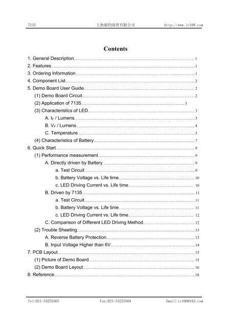
Contents<br />
1. General Description………………………………………………………………………………… 1<br />
2. Features……………………………………………………………………………………...…………. 1<br />
3. Ordering Information…………………..……………..……………..…………….. …..…..……….. 1<br />
4. Component List………………………………………………………………………………..……... 2<br />
5. Demo Board User Guide..……………..…………………………... …………...…….…………. 2<br />
(1) Demo Board Circuit…………………………………………………………………………… 2<br />
(2) Application of <strong>7135</strong>……………………………………………..…………….………... 3<br />
(3) Characteristics of <strong>LED</strong>.…….…….………………….……….……….…….…...…………… 3<br />
A. IF / Lumens……………………………………………………….………….….…………. 3<br />
B. VF / Lumens……………………………………………….………….….………………... 4<br />
C. Temperature………………………………………………….………….….…………….. 5<br />
(4) Characteristics of Battery……………………………………….. .…….…………………... 7<br />
6. Quick Start…………………………………………………………………….……….…..………..…. 9<br />
(1) Performance measurement……………………………………………..………..………… 9<br />
A. Directly driven by Battery……………………………….………….….……………… 9<br />
a. Test Circuit………………………………………………………….……….…….... 9<br />
b. Battery Voltage vs. Life time…………………………………….……….…… 10<br />
c. <strong>LED</strong> Driving Current vs. Life time…………..……………………..…..……. 10<br />
B. Driven by <strong>7135</strong>………………………………………………………..……...……........... 11<br />
a. Test Circuit………………………………………………………….……….……… 11<br />
b. Battery Voltage vs. Life time…………………………………….……….…… 11<br />
c. <strong>LED</strong> Driving Current vs. Life time……………………..………….…..…….. 12<br />
C. Comparison of Different <strong>LED</strong> Driving Method…………………………...…….. 12<br />
(2) Trouble Sheeting……………………………….……………….………………..……………. 13<br />
A. Reverse Battery Protection…………………………………………………………... 13<br />
B. Input Voltage Higher than 6V……………………………………………….……….. 14<br />
7. PCB Layout……………………………………………………….……….…..………………………. 15<br />
(1) Picture of Demo Board………………….……………….……………..……..……………... 15<br />
(2) Demo Board Layout……………………….……………….………………..………………... 16<br />
8. Reference……………………………………………………….……….…..………..…………….….. 18<br />
Tel:021-54253565 Fax:021-54253569 Email:ic108@163.com