tps3824-33dbvrg4
tps3824-33dbvrg4
tps3824-33dbvrg4

You also want an ePaper? Increase the reach of your titles
YUMPU automatically turns print PDFs into web optimized ePapers that Google loves.
www.ti.com<br />
FEATURES<br />
Power-On Reset Generator With Fixed Delay<br />
Time of 200 ms (TPS3823/4/5/8)<br />
or 25 ms (TPS3820)<br />
Manual Reset Input (TPS3820/3/5/8)<br />
Reset Output Available in Active-Low<br />
(TPS3820/3/4/5), Active-High (TPS3824/5) and<br />
Open-Drain (TPS3828)<br />
Supply Voltage Supervision Range:<br />
2.5 V, 3 V, 3.3 V, 5 V<br />
Watchdog Timer (TPS3820/3/4/8)<br />
Supply Current of 15 µA (Typ)<br />
SOT23-5 Package<br />
Temperature Range: −40°C to +85°C<br />
APPLICATIONS<br />
Applications Using DSPs, Microcontrollers, or<br />
Microprocessors<br />
Industrial Equipment<br />
Programmable Controls<br />
Automotive Systems<br />
Portable/Battery-Powered Equipment<br />
Intelligent Instruments<br />
Wireless Communications Systems<br />
Notebook/Desktop Computers<br />
DESCRIPTION<br />
The TPS382x family of supervisors provide circuit<br />
initialization and timing supervision, primarily for DSP<br />
and processor-based systems. During power-on,<br />
RESET asserts when the supply voltage V DD becomes<br />
higher than 1.1 V. Thereafter, the supply voltage<br />
supervisor monitors V DD and keeps RESET active as<br />
long as V DD remains below the threshold voltage, V IT−.<br />
An internal timer delays the return of the output to the<br />
inactive state (high) to ensure proper system reset. The<br />
delay time, t d, starts after V DD has risen above the<br />
threshold voltage, V IT−. When the supply voltage drops<br />
below the threshold voltage V IT−, the output becomes<br />
<br />
<br />
<br />
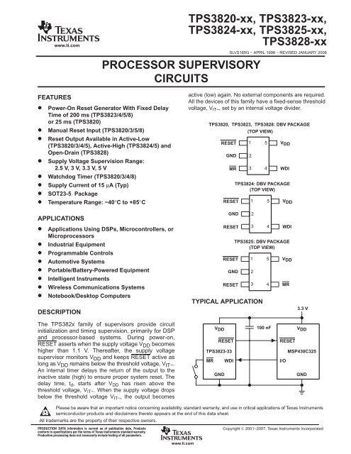
TPS3820-xx, TPS3823-xx,<br />
TPS3824-xx, TPS3825-xx,<br />
TPS3828-xx<br />
SLVS165G − APRIL 1998 − REVISED JANUARY 2008<br />
PROCESSOR SUPERVISORY<br />
CIRCUITS<br />
www.ti.com<br />
active (low) again. No external components are required.<br />
All the devices of this family have a fixed-sense threshold<br />
voltage, V IT−, set by an internal voltage divider.<br />
TPS3820, TPS3823, TPS3828: DBV PACKAGE<br />
(TOP VIEW)<br />
RESET<br />
GND<br />
MR<br />
RESET<br />
GND<br />
RESET<br />
RESET<br />
GND<br />
RESET<br />
RESET<br />
MR WDI<br />
1<br />
2<br />
3<br />
2<br />
3<br />
2<br />
3<br />
5<br />
4<br />
5<br />
4<br />
VDD<br />
WDI<br />
TPS3824: DBV PACKAGE<br />
(TOP VIEW)<br />
1<br />
TPS3825: DBV PACKAGE<br />
(TOP VIEW)<br />
TYPICAL APPLICATION<br />
VDD<br />
TPS3823-33<br />
GND<br />
1<br />
5<br />
4<br />
100 nF<br />
VDD<br />
WDI<br />
VDD<br />
MR<br />
RESET<br />
3.3 V<br />
VDD<br />
MSP430C325<br />
I/O<br />
Please be aware that an important notice concerning availability, standard warranty, and use in critical applications of Texas Instruments<br />
semiconductor products and disclaimers thereto appears at the end of this data sheet.<br />
All trademarks are the property of their respective owners.<br />
GND<br />
Copyright © 2001−2007, Texas Instruments Incorporated
SLVS165G − APRIL 1998 − REVISED JANUARY 2008<br />
DESCRIPTION (Continued)<br />
2<br />
www.ti.com<br />
The TPS3820/3/5/8 devices incorporate a manual reset input, MR. A low level at MR causes RESET to become active.<br />
The TPS3824/5 devices include a high-level output RESET. TPS3820/3/4/8 have a watchdog timer that is periodically<br />
triggered by a positive or negative transition at WDI. When the supervising system fails to retrigger the watchdog circuit<br />
within the time-out interval, t tout, RESET becomes active for the time period t d. This event also reinitializes the watchdog<br />
timer. Leaving WDI unconnected disables the watchdog. In applications where the input to the WDI pin may be active<br />
(transitioning high and low) when the TPS3820/3/4/8 is asserting RESET, the TPS3820/3/4/8 does not return to a non-reset<br />
state when the input voltage is above V T. If the application requires that input to WDI is active when RESET is asserted,<br />
WDI must be decoupled from the active signal. This decoupling can be accomplished by using an N-channel FET in series<br />
with the WDI pin, with the gate of the FET connected to the RESET output as shown in Figure 1.<br />
TPS3824<br />
Figure 1<br />
WDI<br />
RESET<br />
WDI External<br />
The product spectrum is designed for supply voltages of 2.5 V, 3 V, 3.3 V, and 5 V. The circuits are available in an SOT23-5<br />
package. The TPS382x devices are characterized for operation over a temperature range of −40°C to +85°C.<br />
PACKAGE INFORMATION (1)<br />
DEVICE NAME DEVICE NAME THRESHOLD VOLTAGE (2) MARKING<br />
TPS3820-33DBVT (3) TPS3820-33DBVR (4) 2.93 V PDEI<br />
TPS3820-50DBVT (3) TPS3820-50DBVR (4) 4.55 V PDDI<br />
TPS3823-25DBVT (3) TPS3823-25DBVR (4) 2.25 V PAPI<br />
TPS3823-30DBVT (3) TPS3823-30DBVR (4) 2.63 V PAQI<br />
TPS3823-33DBVT (3) TPS3823-33DBVR (4) 2.93 V PARI<br />
TPS3823-50DBVT (3) TPS3823-50DBVR (4) 4.55 V PASI<br />
TPS3824-25DBVT (3) TPS3824-25DBVR (4) 2.25 V PATI<br />
TPS3824-30DBVT (3) TPS3824-30DBVR (4) 2.63 V PAUI<br />
TPS3824-33DBVT (3) TPS3824-33DBVR (4) 2.93 V PAVI<br />
TPS3824-50DBVT (3) TPS3824-50DBVR (4) 4.55 V PAWI<br />
TPS3825-33DBVT (3) TPS3825-33DBVR (4) 2.93 V PDGI<br />
TPS3825-50DBVT (3) TPS3825-50DBVR (4) 4.55 V PDFI<br />
TPS3828-33DBVT (3) TPS3828-33DBVR (4) 2.93 V PDII<br />
TPS3828-50DBVT (3) TPS3828-50DBVR (4) 4.55 V PDHI<br />
(1) For the most current package and ordering information see the Package Option Addendum at<br />
the end of this document, or see the TI web site at www.ti.com.<br />
(2) For other threshold voltage versions, please contact the local TI sales office.<br />
(3) The DBVT package indicates tape and reel of 250 parts.<br />
(4) The DBVR package indicates tape and reel of 3000 parts.
www.ti.com<br />
FUNCTION/TRUTH TABLE<br />
INPUTS OUTPUTS<br />
MR (1) VDD > VIT RESET RESET (2)<br />
L 0 L H<br />
L 1 L H<br />
H 0 L H<br />
H 1 H L<br />
(1) TPS3820/3/5/8<br />
(2) TPS3824/5<br />
FUNCTIONAL BLOCK DIAGRAM<br />
MR (2)<br />
WDI<br />
TIMING DIAGRAM<br />
VIT<br />
VDD<br />
1.1 V<br />
RESET<br />
WDI<br />
undefined<br />
V DD<br />
52 kΩ<br />
Auto−Reset<br />
Oscillator<br />
NOTES: (1) TPS3824/5<br />
(2) TPS3820/3/5/8<br />
+<br />
_<br />
V REF<br />
40 kΩ<br />
RESET<br />
Logic<br />
Transition<br />
Detector<br />
<br />
<br />
<br />
SLVS165G − APRIL 1998 − REVISED JANUARY 2008<br />
Watchdog<br />
Timer Logic<br />
td td tt(out) td<br />
RESET (1)<br />
RESET<br />
undefined<br />
3
SLVS165G − APRIL 1998 − REVISED JANUARY 2008<br />
4<br />
www.ti.com<br />
This integrated circuit can be damaged by ESD. Texas Instruments recommends that all integrated circuits be handled with<br />
appropriate precautions. Failure to observe proper handling and installation procedures can cause damage.<br />
ESD damage can range from subtle performance degradation to complete device failure. Precision integrated circuits may be more susceptible<br />
to damage because very small parametric changes could cause the device not to meet its published specifications.<br />
ABSOLUTE MAXIMUM RATINGS (1)<br />
Over operating free-air temperature range, unless otherwise noted.<br />
Supply voltage, V (1)<br />
DD . . . . . . . . . . . . . . . . . . . . . . . . . . . . . . . . . . . . . . . . . . . . . . . . . . . . . . . . . . . . . . . . . . . . . . +6 V<br />
RESET, RESET, MR, WDI (1) . . . . . . . . . . . . . . . . . . . . . . . . . . . . . . . . . . . . . . . . . . . . . . . −0.3 V to (VDD + 0.3 V)<br />
Maximum low output current, IOL . . . . . . . . . . . . . . . . . . . . . . . . . . . . . . . . . . . . . . . . . . . . . . . . . . . . . . . . . . +5 mA<br />
Maximum high output current, IOH . . . . . . . . . . . . . . . . . . . . . . . . . . . . . . . . . . . . . . . . . . . . . . . . . . . . . . . . . −5 mA<br />
Input clamp current range, IIK (VI < 0 or VI > VDD) . . . . . . . . . . . . . . . . . . . . . . . . . . . . . . . . . . . . . . . . . . ±10 mA<br />
Output clamp current range, IOK (VO < 0 or VO > VDD) . . . . . . . . . . . . . . . . . . . . . . . . . . . . . . . . . . . . . . ±10 mA<br />
Continuous total power dissipation . . . . . . . . . . . . . . . . . . . . . . . . . . . . . . . . . . . . . See Dissipation Rating Table<br />
Operating free-air temperature range, TA . . . . . . . . . . . . . . . . . . . . . . . . . . . . . . . . . . . . . . . . . . . −40°C to +85°C<br />
Storage temperature range, Tstg . . . . . . . . . . . . . . . . . . . . . . . . . . . . . . . . . . . . . . . . . . . . . . . . . . −65°C to +150°C<br />
Soldering temperature . . . . . . . . . . . . . . . . . . . . . . . . . . . . . . . . . . . . . . . . . . . . . . . . . . . . . . . . . . . . . . . . . . . +260°C<br />
(1) Stresses beyond those listed under absolute maximum ratings may cause permanent damage to the device. These are stress ratings only, and<br />
functional operation of the device at these or any other conditions beyond those indicated under recommended operating conditions is not<br />
implied. Exposure to absolute-maximum-rated conditions for extended periods may affect device reliability.<br />
(2) All voltage values are with respect to GND.<br />
DISSIPATION RATING TABLE<br />
PACKAGE<br />
TA ≤ +25°C<br />
POWER RATING<br />
OPERATING FACTOR<br />
ABOVE TA = +25°C<br />
TA = +70°C<br />
POWER RATING<br />
TA = +85°C<br />
POWER RATING<br />
DBV 437 mW 3.5 mW/°C 280 mW 227 mW<br />
RECOMMENDED OPERATING CONDITIONS<br />
MIN MAX UNIT<br />
Supply voltage, VDD 1.1 5.5 V<br />
Input voltage, VI 0 VDD + 0.3 V<br />
High-level input voltage at MR and WDI, VIH 0.7 × VDD V<br />
Low-level input voltage, VIL 0.3 × VDD V<br />
Input transition rise and fall rate at MR or WDI, ∆t/∆V 100 ns/V<br />
Operating free-air temperature range, TA −40 +85 °C
www.ti.com<br />
<br />
<br />
<br />
SLVS165G − APRIL 1998 − REVISED JANUARY 2008<br />
ELECTRICAL CHARACTERISTICS<br />
Over operating free-air temperature range, unless otherwise noted.<br />
PARAMETER TEST CONDITIONS MIN TYP MAX UNIT<br />
TPS382x-25<br />
VDD = VIT− + 0.2 V<br />
IOH = −20 µA<br />
VOH<br />
VOL<br />
VIT− VIT−<br />
Vhys Vhys<br />
High-level output voltage<br />
Low-level output voltage<br />
RESET TPS382x-30<br />
TPS382x-33<br />
TPS382x-50<br />
TPS3824-25<br />
TPS3825-25<br />
TPS3824-30<br />
TPS3825-30<br />
RESET<br />
TPS3824-33<br />
TPS3825-33<br />
TPS3824-50<br />
TPS3825-50<br />
TPS3824-25<br />
TPS3825-25<br />
VDD = VIT− + 0.2 V<br />
IOH = −30 µA<br />
VDD = VIT− + 0.2 V<br />
IOH = −120 µA<br />
VDD ≥ 1.8 V, IOH = −100 µA<br />
VDD ≥ 1.8 V, IOH = −150 µA<br />
VDD = VIT− + 0.2 V<br />
IOL = 1 mA<br />
RESET<br />
TPS3824-30<br />
TPS3825-30<br />
TPS3824-33<br />
TPS3825-33<br />
VDD VDD = VIT− VIT− + 0.2 V<br />
IOL = 1.2 mA<br />
TPS3824-50 VDD = VIT− + 0.2 V<br />
TPS3825-50 IOL = 3 mA<br />
TPS382x-25<br />
VDD = VIT− − 0.2 V<br />
IOL = 1 mA<br />
RESET TPS382x-30 VDD VDD = VIT− VIT− −0.2 V<br />
RESET<br />
TPS382x-33 IOL = 1.2 mA<br />
TPS382x-50<br />
VDD = VIT− − 0.2 V<br />
IOL = 3 mA<br />
0.8 0.8 × VDD VDD<br />
VDD − 1.5 V<br />
0.8 0.8 × VDD VDD<br />
V<br />
V<br />
0.4 V<br />
0.4 V<br />
Power-up reset voltage (1) VDD ≥ 1.1 V, IOL = 20 µA 0.4 V<br />
TPS382x-25 2.21 2.25 2.30<br />
TPS382x-30<br />
TPS382x-33<br />
TA TA = 0°C to +85°C<br />
2.59 2.63 2.69<br />
2.88 2.93 3<br />
Negative-going input threshold TPS382x-50 4.49 4.55 4.64<br />
voltage (2) voltage<br />
TPS382x-25 2.20 2.25 2.30<br />
Hysteresis at VDD VDD input<br />
TPS382x-30<br />
TPS382x-33<br />
TA TA = −40°C to +85°C<br />
2.57 2.63 2.69<br />
2.86 2.93 3<br />
TPS382x-50 4.46 4.55 4.64<br />
TPS382x-25<br />
TPS382x-30 30<br />
TPS382x-33<br />
TPS382x-50 50<br />
(1) The lowest supply voltage at which RESET becomes active. tr, VDD ≥ 15 µs/V.<br />
(2) To ensure best stability of the threshold voltage, a bypass capacitor (ceramic, 0.1 µF) should be placed near the supply terminals.<br />
V<br />
V<br />
mV<br />
5
SLVS165G − APRIL 1998 − REVISED JANUARY 2008<br />
6<br />
www.ti.com<br />
ELECTRICAL CHARACTERISTICS (continued)<br />
Over operating free-air temperature range, unless otherwise noted.<br />
PARAMETER TEST CONDITIONS MIN TYP MAX UNIT<br />
IIH(AV) Average high-level input current<br />
IIL(AV)<br />
IIH<br />
IIL IIL<br />
IOS IOS<br />
IDD<br />
Average low-level input current<br />
High-level input current<br />
Low-level input current current<br />
Output short-circuit<br />
current(1) current<br />
Supply current<br />
WDI<br />
WDI = VDD,<br />
time average (dc = 88%)<br />
WDI = 0.3 V, VDD = 5.5 V<br />
time average (dc = 12%)<br />
−15<br />
WDI WDI = VDD 140 190 µA<br />
MR<br />
MR = VDD × 0.7,<br />
VDD = 5.5 V<br />
−40 −60<br />
WDI WDI = 0.3 V, VDD = 5.5 V 140 190<br />
MR MR = 0.3 V, VDD = 5.5 V −110 −160<br />
TPS382x-25<br />
RESET TPS382x-30 VDD VDD = VIT, VIT, max + 0.2 V, −400<br />
RESET<br />
max + 0.2 V,<br />
−400<br />
TPS382x-33 VO VO = 0 V<br />
TPS382x-50<br />
WDI and MR unconnected,<br />
Outputs unconnected<br />
120<br />
−800<br />
µAA<br />
15 25 µA<br />
Internal pullup resistor at MR 52 kΩ<br />
Ci Input capacitance at MR, WDI VI = 0 V to 5.5 V 5 pF<br />
(1) The RESET short-circuit current is the maximum pullup current when RESET is driven low by a µP bidirectional reset pin.<br />
TIMING REQUIREMENTS AT RL = 1 MΩ, CL = 50 PF, TA = 25°C<br />
At RL = 1 MΩ, CL = 50 pF, TA = +25°C.<br />
PARAMETER TEST CONDITIONS MIN MAX UNIT<br />
at VDD VDD = VIT− + 0.2 V, VDD = VIT- − 0.2 V 6 µs<br />
tw tw Pulse width at MR VDD ≥ VIT− + 0.2 V, VIL = 0.3 x VDD, VIH = 0.7 x VDD 1 µs<br />
at WDI VDD ≥ VIT− + 0.2 V, VIL = 0.3 x VDD, VIH = 0.7 x VDD 100 ns<br />
SWITCHING CHARACTERISTICS<br />
At RL = 1 MΩ, CL = 50 pF, TA = +25°C.<br />
PARAMETER TEST CONDITIONS MIN TYP MAX UNIT<br />
ttout ttout Watchdog time out<br />
TPS3820<br />
TPS3823/4/8<br />
VDD VDD ≥ VIT− VIT− + 0.2 V,<br />
See timing diagram<br />
112<br />
0.9<br />
200<br />
1.6<br />
310<br />
2.5<br />
ms<br />
s<br />
td td<br />
tPHL tPHL<br />
tPLH tPLH<br />
Delay time<br />
Propagation (delay) time,<br />
high-to-low-level output<br />
Propagation (delay) time,<br />
low-to-high-level output<br />
TPS3820 VDD VDD ≥ VIT− VIT− +0.2 V, 15 25 37<br />
TPS3823/4/5/8<br />
See timing diagram 120 200 300<br />
MR to RESET delay<br />
(TPS3820/3/5/8)<br />
VDD to RESET delay<br />
MR to RESET delay (TPS3824/5)<br />
VDD ≥ VIT− +0.2 V,<br />
VIL = 0.3 x VDD,<br />
VIH = 0.7 x VDD<br />
VIL = VIT- - 0.2 V,<br />
VIH = VIT- + 0.2 V<br />
VDD ≥ VIT− +0.2 V,<br />
VIL = 0.3 x VDD,<br />
VIH = 0.7 x VDD<br />
VDD to RESET delay (TPS3824/5) VIL = VIT- - 0.2 V,<br />
VIH = VIT- + 0.2 V<br />
0.1<br />
25<br />
0.1<br />
25<br />
ms<br />
µs<br />
µs
Normalized Input Threshold Voltage − V IT (T A ), V IT (25°C)<br />
A<br />
µ<br />
− Input Current −<br />
I I<br />
www.ti.com<br />
1.001<br />
1<br />
0.999<br />
0.998<br />
0.997<br />
0.996<br />
0.995<br />
−40<br />
50<br />
0<br />
−50<br />
−100<br />
−150<br />
NORMALIZED INPUT THRESHOLD VOLTAGE<br />
vs<br />
FREE-AIR TEMPERATURE AT V DD<br />
−15 10 35 60 85<br />
TA − Free-Air Temperature − °C<br />
VDD = 5.5 V<br />
WDI = Open<br />
−40°C<br />
Figure 2<br />
INPUT CURRENT<br />
vs<br />
INPUT VOLTAGE AT MR<br />
85°C<br />
−200<br />
−1 0 1 2 3 4 5 6<br />
VI − Input Voltage at MR − V<br />
Figure 4<br />
TYPICAL CHARACTERISTICS<br />
A<br />
IDD− Supply Current − µ<br />
VOL− Low-Level Output Voltage − V<br />
19<br />
17<br />
15<br />
13<br />
11<br />
9<br />
7<br />
5<br />
3<br />
1<br />
−1<br />
−0.5<br />
3<br />
2.5<br />
2<br />
1.5<br />
1<br />
0.5<br />
0<br />
0<br />
MR = Open<br />
WDI = Open<br />
TA = 25°C<br />
<br />
<br />
<br />
SLVS165G − APRIL 1998 − REVISED JANUARY 2008<br />
SUPPLY CURRENT<br />
vs<br />
SUPPLY VOLTAGE<br />
0.5 1.5 2.5 3.5 4.5 5.5 6.5<br />
VDD − Supply Voltage − V<br />
Figure 3<br />
Figure 5<br />
TPS382x-33<br />
LOW-LEVEL OUTPUT VOLTAGE<br />
vs<br />
LOW-LEVEL OUTPUT CURRENT<br />
VDD = 2.66 V<br />
WDI = Open<br />
MR = Open<br />
85°C<br />
−40°C<br />
1 2 3 4 5 6 7 8 9 10<br />
IOL − Low-Level Output Current − mA<br />
7
SLVS165G − APRIL 1998 − REVISED JANUARY 2008<br />
8<br />
VOH − High-Level Output Voltage − V<br />
3.5<br />
3<br />
2.5<br />
2<br />
1.5<br />
1<br />
0.5<br />
HIGH-LEVEL OUTPUT VOLTAGE<br />
vs<br />
HIGH-LEVEL OUTPUT CURRENT<br />
85°C<br />
0<br />
0 −50 −100 −150 −200 −250<br />
IOH − High-Level Output Current − µA<br />
Figure 6<br />
s<br />
µ<br />
− Minimum Pulse Duration at VDD−<br />
t w<br />
10<br />
8<br />
6<br />
4<br />
2<br />
0<br />
0<br />
TYPICAL CHARACTERISTICS<br />
VDD = 3.2 V<br />
WDI = Open<br />
MR = Open<br />
−40°C<br />
VOH − High-Level Output Voltage − V<br />
Figure 8<br />
6<br />
5<br />
4<br />
3<br />
2<br />
1<br />
0<br />
0<br />
MINIMUM PULSE DURATION AT V DD<br />
vs<br />
V DD THRESHOLD OVERDRIVE<br />
200 400 600 800<br />
VDD − Threshold Overdrive − mV<br />
HIGH-LEVEL OUTPUT VOLTAGE<br />
vs<br />
HIGH-LEVEL OUTPUT CURRENT<br />
85°C<br />
Figure 7<br />
www.ti.com<br />
VDD = 5.5 V<br />
WDI = Open<br />
MR = Open<br />
−40°C<br />
−100 −200 −300 −400 −500 −600 −700<br />
IOH − High-Level Output Current − µA<br />
WDI = Open<br />
MR = Open<br />
1000
Revision History<br />
DATE REV PAGE SECTION DESCRIPTION<br />
1/08 G<br />
6/07 F<br />
2 Description Deleted last paragraph.<br />
3 Functional Block Diagram Replaced diagram.<br />
Front Page — Updated front page.<br />
3 Function/Truth Table Corrected Note (2) from PS3820/3/5/8 to TPS3824/5.<br />
NOTE: Page numbers for previous revisions may differ from page numbers in the current version.
PACKAGING INFORMATION<br />
Orderable Device Status (1)<br />
Package<br />
Type<br />
Package<br />
Drawing<br />
Pins Package<br />
Qty<br />
TPS3820-33DBVR ACTIVE SOT-23 DBV 5 3000 Green (RoHS &<br />
no Sb/Br)<br />
TPS3820-33DBVRG4 ACTIVE SOT-23 DBV 5 3000 Green (RoHS &<br />
no Sb/Br)<br />
TPS3820-33DBVT ACTIVE SOT-23 DBV 5 250 Green (RoHS &<br />
no Sb/Br)<br />
TPS3820-33DBVTG4 ACTIVE SOT-23 DBV 5 250 Green (RoHS &<br />
no Sb/Br)<br />
TPS3820-50DBVR ACTIVE SOT-23 DBV 5 3000 Green (RoHS &<br />
no Sb/Br)<br />
TPS3820-50DBVRG4 ACTIVE SOT-23 DBV 5 3000 Green (RoHS &<br />
no Sb/Br)<br />
TPS3820-50DBVT ACTIVE SOT-23 DBV 5 250 Green (RoHS &<br />
no Sb/Br)<br />
TPS3820-50DBVTG4 ACTIVE SOT-23 DBV 5 250 Green (RoHS &<br />
no Sb/Br)<br />
TPS3823-25DBVR ACTIVE SOT-23 DBV 5 3000 Green (RoHS &<br />
no Sb/Br)<br />
TPS3823-25DBVRG4 ACTIVE SOT-23 DBV 5 3000 Green (RoHS &<br />
no Sb/Br)<br />
TPS3823-25DBVT ACTIVE SOT-23 DBV 5 250 Green (RoHS &<br />
no Sb/Br)<br />
TPS3823-25DBVTG4 ACTIVE SOT-23 DBV 5 250 Green (RoHS &<br />
no Sb/Br)<br />
TPS3823-30DBVR ACTIVE SOT-23 DBV 5 3000 Green (RoHS &<br />
no Sb/Br)<br />
TPS3823-30DBVRG4 ACTIVE SOT-23 DBV 5 3000 Green (RoHS &<br />
no Sb/Br)<br />
TPS3823-30DBVT ACTIVE SOT-23 DBV 5 250 Green (RoHS &<br />
no Sb/Br)<br />
TPS3823-30DBVTG4 ACTIVE SOT-23 DBV 5 250 Green (RoHS &<br />
no Sb/Br)<br />
TPS3823-33DBVR ACTIVE SOT-23 DBV 5 3000 Green (RoHS &<br />
no Sb/Br)<br />
TPS3823-33DBVRG4 ACTIVE SOT-23 DBV 5 3000 Green (RoHS &<br />
no Sb/Br)<br />
TPS3823-33DBVT ACTIVE SOT-23 DBV 5 250 Green (RoHS &<br />
no Sb/Br)<br />
TPS3823-33DBVTG4 ACTIVE SOT-23 DBV 5 250 Green (RoHS &<br />
no Sb/Br)<br />
TPS3823-50DBVR ACTIVE SOT-23 DBV 5 3000 Green (RoHS &<br />
no Sb/Br)<br />
TPS3823-50DBVRG4 ACTIVE SOT-23 DBV 5 3000 Green (RoHS &<br />
no Sb/Br)<br />
TPS3823-50DBVT ACTIVE SOT-23 DBV 5 250 Green (RoHS &<br />
no Sb/Br)<br />
TPS3823-50DBVTG4 ACTIVE SOT-23 DBV 5 250 Green (RoHS &<br />
no Sb/Br)<br />
TPS3824-25DBVR ACTIVE SOT-23 DBV 5 3000 Green (RoHS &<br />
no Sb/Br)<br />
PACKAGE OPTION ADDENDUM<br />
www.ti.com 17-Jan-2008<br />
Addendum-Page 1<br />
Eco Plan (2) Lead/Ball Finish MSL Peak Temp (3)<br />
CU NIPDAU Level-1-260C-UNLIM<br />
CU NIPDAU Level-1-260C-UNLIM<br />
CU NIPDAU Level-1-260C-UNLIM<br />
CU NIPDAU Level-1-260C-UNLIM<br />
CU NIPDAU Level-1-260C-UNLIM<br />
CU NIPDAU Level-1-260C-UNLIM<br />
CU NIPDAU Level-1-260C-UNLIM<br />
CU NIPDAU Level-1-260C-UNLIM<br />
CU NIPDAU Level-1-260C-UNLIM<br />
CU NIPDAU Level-1-260C-UNLIM<br />
CU NIPDAU Level-1-260C-UNLIM<br />
CU NIPDAU Level-1-260C-UNLIM<br />
CU NIPDAU Level-1-260C-UNLIM<br />
CU NIPDAU Level-1-260C-UNLIM<br />
CU NIPDAU Level-1-260C-UNLIM<br />
CU NIPDAU Level-1-260C-UNLIM<br />
CU NIPDAU Level-1-260C-UNLIM<br />
CU NIPDAU Level-1-260C-UNLIM<br />
CU NIPDAU Level-1-260C-UNLIM<br />
CU NIPDAU Level-1-260C-UNLIM<br />
CU NIPDAU Level-1-260C-UNLIM<br />
CU NIPDAU Level-1-260C-UNLIM<br />
CU NIPDAU Level-1-260C-UNLIM<br />
CU NIPDAU Level-1-260C-UNLIM<br />
CU NIPDAU Level-1-260C-UNLIM
Orderable Device Status (1)<br />
Package<br />
Type<br />
Package<br />
Drawing<br />
Pins Package<br />
Qty<br />
TPS3824-25DBVRG4 ACTIVE SOT-23 DBV 5 3000 Green (RoHS &<br />
no Sb/Br)<br />
TPS3824-25DBVT ACTIVE SOT-23 DBV 5 250 Green (RoHS &<br />
no Sb/Br)<br />
TPS3824-25DBVTG4 ACTIVE SOT-23 DBV 5 250 Green (RoHS &<br />
no Sb/Br)<br />
TPS3824-30DBVR ACTIVE SOT-23 DBV 5 3000 Green (RoHS &<br />
no Sb/Br)<br />
TPS3824-30DBVRG4 ACTIVE SOT-23 DBV 5 3000 Green (RoHS &<br />
no Sb/Br)<br />
TPS3824-30DBVT ACTIVE SOT-23 DBV 5 250 Green (RoHS &<br />
no Sb/Br)<br />
TPS3824-30DBVTG4 ACTIVE SOT-23 DBV 5 250 Green (RoHS &<br />
no Sb/Br)<br />
TPS3824-33DBVR ACTIVE SOT-23 DBV 5 3000 Green (RoHS &<br />
no Sb/Br)<br />
TPS3824-33DBVRG4 ACTIVE SOT-23 DBV 5 3000 Green (RoHS &<br />
no Sb/Br)<br />
TPS3824-33DBVT ACTIVE SOT-23 DBV 5 250 Green (RoHS &<br />
no Sb/Br)<br />
TPS3824-33DBVTG4 ACTIVE SOT-23 DBV 5 250 Green (RoHS &<br />
no Sb/Br)<br />
TPS3824-50DBVR ACTIVE SOT-23 DBV 5 3000 Green (RoHS &<br />
no Sb/Br)<br />
TPS3824-50DBVRG4 ACTIVE SOT-23 DBV 5 3000 Green (RoHS &<br />
no Sb/Br)<br />
TPS3824-50DBVT ACTIVE SOT-23 DBV 5 250 Green (RoHS &<br />
no Sb/Br)<br />
TPS3824-50DBVTG4 ACTIVE SOT-23 DBV 5 250 Green (RoHS &<br />
no Sb/Br)<br />
TPS3825-33DBVR ACTIVE SOT-23 DBV 5 3000 Green (RoHS &<br />
no Sb/Br)<br />
TPS3825-33DBVRG4 ACTIVE SOT-23 DBV 5 3000 Green (RoHS &<br />
no Sb/Br)<br />
TPS3825-33DBVT ACTIVE SOT-23 DBV 5 250 Green (RoHS &<br />
no Sb/Br)<br />
TPS3825-33DBVTG4 ACTIVE SOT-23 DBV 5 250 Green (RoHS &<br />
no Sb/Br)<br />
TPS3825-50DBVR ACTIVE SOT-23 DBV 5 3000 Green (RoHS &<br />
no Sb/Br)<br />
TPS3825-50DBVRG4 ACTIVE SOT-23 DBV 5 3000 Green (RoHS &<br />
no Sb/Br)<br />
TPS3825-50DBVT ACTIVE SOT-23 DBV 5 250 Green (RoHS &<br />
no Sb/Br)<br />
TPS3825-50DBVTG4 ACTIVE SOT-23 DBV 5 250 Green (RoHS &<br />
no Sb/Br)<br />
TPS3828-33DBVR ACTIVE SOT-23 DBV 5 3000 Green (RoHS &<br />
no Sb/Br)<br />
TPS3828-33DBVRG4 ACTIVE SOT-23 DBV 5 3000 Green (RoHS &<br />
no Sb/Br)<br />
TPS3828-33DBVT ACTIVE SOT-23 DBV 5 250 Green (RoHS &<br />
no Sb/Br)<br />
PACKAGE OPTION ADDENDUM<br />
www.ti.com 17-Jan-2008<br />
Addendum-Page 2<br />
Eco Plan (2) Lead/Ball Finish MSL Peak Temp (3)<br />
CU NIPDAU Level-1-260C-UNLIM<br />
CU NIPDAU Level-1-260C-UNLIM<br />
CU NIPDAU Level-1-260C-UNLIM<br />
CU NIPDAU Level-1-260C-UNLIM<br />
CU NIPDAU Level-1-260C-UNLIM<br />
CU NIPDAU Level-1-260C-UNLIM<br />
CU NIPDAU Level-1-260C-UNLIM<br />
CU NIPDAU Level-1-260C-UNLIM<br />
CU NIPDAU Level-1-260C-UNLIM<br />
CU NIPDAU Level-1-260C-UNLIM<br />
CU NIPDAU Level-1-260C-UNLIM<br />
CU NIPDAU Level-1-260C-UNLIM<br />
CU NIPDAU Level-1-260C-UNLIM<br />
CU NIPDAU Level-1-260C-UNLIM<br />
CU NIPDAU Level-1-260C-UNLIM<br />
CU NIPDAU Level-1-260C-UNLIM<br />
CU NIPDAU Level-1-260C-UNLIM<br />
CU NIPDAU Level-1-260C-UNLIM<br />
CU NIPDAU Level-1-260C-UNLIM<br />
CU NIPDAU Level-1-260C-UNLIM<br />
CU NIPDAU Level-1-260C-UNLIM<br />
CU NIPDAU Level-1-260C-UNLIM<br />
CU NIPDAU Level-1-260C-UNLIM<br />
CU NIPDAU Level-1-260C-UNLIM<br />
CU NIPDAU Level-1-260C-UNLIM<br />
CU NIPDAU Level-1-260C-UNLIM
Orderable Device Status (1)<br />
Package<br />
Type<br />
Package<br />
Drawing<br />
Pins Package<br />
Qty<br />
TPS3828-33DBVTG4 ACTIVE SOT-23 DBV 5 250 Green (RoHS &<br />
no Sb/Br)<br />
TPS3828-50DBVR ACTIVE SOT-23 DBV 5 3000 Green (RoHS &<br />
no Sb/Br)<br />
TPS3828-50DBVRG4 ACTIVE SOT-23 DBV 5 3000 Green (RoHS &<br />
no Sb/Br)<br />
TPS3828-50DBVT ACTIVE SOT-23 DBV 5 250 Green (RoHS &<br />
no Sb/Br)<br />
TPS3828-50DBVTG4 ACTIVE SOT-23 DBV 5 250 Green (RoHS &<br />
no Sb/Br)<br />
Eco Plan (2) Lead/Ball Finish MSL Peak Temp (3)<br />
CU NIPDAU Level-1-260C-UNLIM<br />
CU NIPDAU Level-1-260C-UNLIM<br />
CU NIPDAU Level-1-260C-UNLIM<br />
CU NIPDAU Level-1-260C-UNLIM<br />
CU NIPDAU Level-1-260C-UNLIM<br />
(1) The marketing status values are defined as follows:<br />
ACTIVE: Product device recommended for new designs.<br />
LIFEBUY: TI has announced that the device will be discontinued, and a lifetime-buy period is in effect.<br />
NRND: Not recommended for new designs. Device is in production to support existing customers, but TI does not recommend using this part in<br />
a new design.<br />
PREVIEW: Device has been announced but is not in production. Samples may or may not be available.<br />
OBSOLETE: TI has discontinued the production of the device.<br />
(2) Eco Plan - The planned eco-friendly classification: Pb-Free (RoHS), Pb-Free (RoHS Exempt), or Green (RoHS & no Sb/Br) - please check<br />
http://www.ti.com/productcontent for the latest availability information and additional product content details.<br />
TBD: The Pb-Free/Green conversion plan has not been defined.<br />
Pb-Free (RoHS): TI's terms "Lead-Free" or "Pb-Free" mean semiconductor products that are compatible with the current RoHS requirements<br />
for all 6 substances, including the requirement that lead not exceed 0.1% by weight in homogeneous materials. Where designed to be soldered<br />
at high temperatures, TI Pb-Free products are suitable for use in specified lead-free processes.<br />
Pb-Free (RoHS Exempt): This component has a RoHS exemption for either 1) lead-based flip-chip solder bumps used between the die and<br />
package, or 2) lead-based die adhesive used between the die and leadframe. The component is otherwise considered Pb-Free (RoHS<br />
compatible) as defined above.<br />
Green (RoHS & no Sb/Br): TI defines "Green" to mean Pb-Free (RoHS compatible), and free of Bromine (Br) and Antimony (Sb) based flame<br />
retardants (Br or Sb do not exceed 0.1% by weight in homogeneous material)<br />
(3) MSL, Peak Temp. -- The Moisture Sensitivity Level rating according to the JEDEC industry standard classifications, and peak solder<br />
temperature.<br />
PACKAGE OPTION ADDENDUM<br />
www.ti.com 17-Jan-2008<br />
Important Information and Disclaimer:The information provided on this page represents TI's knowledge and belief as of the date that it is<br />
provided. TI bases its knowledge and belief on information provided by third parties, and makes no representation or warranty as to the<br />
accuracy of such information. Efforts are underway to better integrate information from third parties. TI has taken and continues to take<br />
reasonable steps to provide representative and accurate information but may not have conducted destructive testing or chemical analysis on<br />
incoming materials and chemicals. TI and TI suppliers consider certain information to be proprietary, and thus CAS numbers and other limited<br />
information may not be available for release.<br />
In no event shall TI's liability arising out of such information exceed the total purchase price of the TI part(s) at issue in this document sold by TI<br />
to Customer on an annual basis.<br />
Addendum-Page 3
TAPE AND REEL BOX INFORMATION<br />
Device Package Pins Site Reel<br />
Diameter<br />
(mm)<br />
PACKAGE MATERIALS INFORMATION<br />
www.ti.com 17-Jan-2008<br />
Reel<br />
Width<br />
(mm)<br />
A0 (mm) B0 (mm) K0 (mm) P1<br />
(mm)<br />
W<br />
(mm)<br />
Pin1<br />
Quadrant<br />
TPS3820-33DBVR DBV 5 SITE 48 179 8 3.2 3.2 1.4 4 8 Q3<br />
TPS3820-33DBVR DBV 5 SITE 40 180 9 3.15 3.2 1.4 4 8 Q3<br />
TPS3820-33DBVT DBV 5 SITE 48 179 8 3.2 3.2 1.4 4 8 Q3<br />
TPS3820-50DBVR DBV 5 SITE 48 179 8 3.2 3.2 1.4 4 8 Q3<br />
TPS3820-50DBVT DBV 5 SITE 48 179 8 3.2 3.2 1.4 4 8 Q3<br />
TPS3823-25DBVR DBV 5 SITE 48 179 8 3.2 3.2 1.4 4 8 Q3<br />
TPS3823-25DBVT DBV 5 SITE 48 179 8 3.2 3.2 1.4 4 8 Q3<br />
TPS3823-30DBVR DBV 5 SITE 48 179 8 3.2 3.2 1.4 4 8 Q3<br />
TPS3823-30DBVT DBV 5 SITE 48 179 8 3.2 3.2 1.4 4 8 Q3<br />
TPS3823-33DBVR DBV 5 SITE 48 179 8 3.2 3.2 1.4 4 8 Q3<br />
TPS3823-33DBVT DBV 5 SITE 48 179 8 3.2 3.2 1.4 4 8 Q3<br />
TPS3823-50DBVR DBV 5 SITE 48 179 8 3.2 3.2 1.4 4 8 Q3<br />
TPS3823-50DBVT DBV 5 SITE 48 179 8 3.2 3.2 1.4 4 8 Q3<br />
TPS3824-25DBVR DBV 5 SITE 48 179 8 3.2 3.2 1.4 4 8 Q3<br />
TPS3824-25DBVT DBV 5 SITE 48 179 8 3.2 3.2 1.4 4 8 Q3<br />
TPS3824-30DBVR DBV 5 SITE 48 179 8 3.2 3.2 1.4 4 8 Q3<br />
TPS3824-30DBVT DBV 5 SITE 48 179 8 3.2 3.2 1.4 4 8 Q3<br />
TPS3824-33DBVR DBV 5 SITE 48 179 8 3.2 3.2 1.4 4 8 Q3<br />
TPS3824-33DBVT DBV 5 SITE 48 179 8 3.2 3.2 1.4 4 8 Q3<br />
Pack Materials-Page 1
Device Package Pins Site Reel<br />
Diameter<br />
(mm)<br />
Reel<br />
Width<br />
(mm)<br />
A0 (mm) B0 (mm) K0 (mm) P1<br />
(mm)<br />
W<br />
(mm)<br />
Pin1<br />
Quadrant<br />
TPS3824-50DBVR DBV 5 SITE 48 179 8 3.2 3.2 1.4 4 8 Q3<br />
TPS3824-50DBVT DBV 5 SITE 48 179 8 3.2 3.2 1.4 4 8 Q3<br />
TPS3825-33DBVR DBV 5 SITE 48 179 8 3.2 3.2 1.4 4 8 Q3<br />
TPS3825-33DBVT DBV 5 SITE 48 179 8 3.2 3.2 1.4 4 8 Q3<br />
TPS3825-50DBVR DBV 5 SITE 48 179 8 3.2 3.2 1.4 4 8 Q3<br />
TPS3825-50DBVT DBV 5 SITE 48 179 8 3.2 3.2 1.4 4 8 Q3<br />
TPS3828-33DBVR DBV 5 SITE 48 179 8 3.2 3.2 1.4 4 8 Q3<br />
TPS3828-33DBVT DBV 5 SITE 48 179 8 3.2 3.2 1.4 4 8 Q3<br />
TPS3828-50DBVR DBV 5 SITE 48 179 8 3.2 3.2 1.4 4 8 Q3<br />
TPS3828-50DBVT DBV 5 SITE 48 179 8 3.2 3.2 1.4 4 8 Q3<br />
Device Package Pins Site Length (mm) Width (mm) Height (mm)<br />
TPS3820-33DBVR DBV 5 SITE 48 195.0 200.0 45.0<br />
TPS3820-33DBVR DBV 5 SITE 40 182.0 182.0 20.0<br />
TPS3820-33DBVT DBV 5 SITE 48 195.0 200.0 45.0<br />
TPS3820-50DBVR DBV 5 SITE 48 195.0 200.0 45.0<br />
TPS3820-50DBVT DBV 5 SITE 48 195.0 200.0 45.0<br />
TPS3823-25DBVR DBV 5 SITE 48 195.0 200.0 45.0<br />
TPS3823-25DBVT DBV 5 SITE 48 195.0 200.0 45.0<br />
PACKAGE MATERIALS INFORMATION<br />
www.ti.com 17-Jan-2008<br />
Pack Materials-Page 2
Device Package Pins Site Length (mm) Width (mm) Height (mm)<br />
TPS3823-30DBVR DBV 5 SITE 48 195.0 200.0 45.0<br />
TPS3823-30DBVT DBV 5 SITE 48 195.0 200.0 45.0<br />
TPS3823-33DBVR DBV 5 SITE 48 195.0 200.0 45.0<br />
TPS3823-33DBVT DBV 5 SITE 48 195.0 200.0 45.0<br />
TPS3823-50DBVR DBV 5 SITE 48 195.0 200.0 45.0<br />
TPS3823-50DBVT DBV 5 SITE 48 195.0 200.0 45.0<br />
TPS3824-25DBVR DBV 5 SITE 48 195.0 200.0 45.0<br />
TPS3824-25DBVT DBV 5 SITE 48 195.0 200.0 45.0<br />
TPS3824-30DBVR DBV 5 SITE 48 195.0 200.0 45.0<br />
TPS3824-30DBVT DBV 5 SITE 48 195.0 200.0 45.0<br />
TPS3824-33DBVR DBV 5 SITE 48 195.0 200.0 45.0<br />
TPS3824-33DBVT DBV 5 SITE 48 195.0 200.0 45.0<br />
TPS3824-50DBVR DBV 5 SITE 48 195.0 200.0 45.0<br />
TPS3824-50DBVT DBV 5 SITE 48 195.0 200.0 45.0<br />
TPS3825-33DBVR DBV 5 SITE 48 195.0 200.0 45.0<br />
TPS3825-33DBVT DBV 5 SITE 48 195.0 200.0 45.0<br />
TPS3825-50DBVR DBV 5 SITE 48 195.0 200.0 45.0<br />
TPS3825-50DBVT DBV 5 SITE 48 195.0 200.0 45.0<br />
TPS3828-33DBVR DBV 5 SITE 48 195.0 200.0 45.0<br />
TPS3828-33DBVT DBV 5 SITE 48 195.0 200.0 45.0<br />
TPS3828-50DBVR DBV 5 SITE 48 195.0 200.0 45.0<br />
TPS3828-50DBVT DBV 5 SITE 48 195.0 200.0 45.0<br />
PACKAGE MATERIALS INFORMATION<br />
www.ti.com 17-Jan-2008<br />
Pack Materials-Page 3
IMPORTANT NOTICE<br />
Texas Instruments Incorporated and its subsidiaries (TI) reserve the right to make corrections, modifications, enhancements, improvements,<br />
and other changes to its products and services at any time and to discontinue any product or service without notice. Customers should<br />
obtain the latest relevant information before placing orders and should verify that such information is current and complete. All products are<br />
sold subject to TI’s terms and conditions of sale supplied at the time of order acknowledgment.<br />
TI warrants performance of its hardware products to the specifications applicable at the time of sale in accordance with TI’s standard<br />
warranty. Testing and other quality control techniques are used to the extent TI deems necessary to support this warranty. Except where<br />
mandated by government requirements, testing of all parameters of each product is not necessarily performed.<br />
TI assumes no liability for applications assistance or customer product design. Customers are responsible for their products and<br />
applications using TI components. To minimize the risks associated with customer products and applications, customers should provide<br />
adequate design and operating safeguards.<br />
TI does not warrant or represent that any license, either express or implied, is granted under any TI patent right, copyright, mask work right,<br />
or other TI intellectual property right relating to any combination, machine, or process in which TI products or services are used. Information<br />
published by TI regarding third-party products or services does not constitute a license from TI to use such products or services or a<br />
warranty or endorsement thereof. Use of such information may require a license from a third party under the patents or other intellectual<br />
property of the third party, or a license from TI under the patents or other intellectual property of TI.<br />
Reproduction of TI information in TI data books or data sheets is permissible only if reproduction is without alteration and is accompanied<br />
by all associated warranties, conditions, limitations, and notices. Reproduction of this information with alteration is an unfair and deceptive<br />
business practice. TI is not responsible or liable for such altered documentation. Information of third parties may be subject to additional<br />
restrictions.<br />
Resale of TI products or services with statements different from or beyond the parameters stated by TI for that product or service voids all<br />
express and any implied warranties for the associated TI product or service and is an unfair and deceptive business practice. TI is not<br />
responsible or liable for any such statements.<br />
TI products are not authorized for use in safety-critical applications (such as life support) where a failure of the TI product would reasonably<br />
be expected to cause severe personal injury or death, unless officers of the parties have executed an agreement specifically governing<br />
such use. Buyers represent that they have all necessary expertise in the safety and regulatory ramifications of their applications, and<br />
acknowledge and agree that they are solely responsible for all legal, regulatory and safety-related requirements concerning their products<br />
and any use of TI products in such safety-critical applications, notwithstanding any applications-related information or support that may be<br />
provided by TI. Further, Buyers must fully indemnify TI and its representatives against any damages arising out of the use of TI products in<br />
such safety-critical applications.<br />
TI products are neither designed nor intended for use in military/aerospace applications or environments unless the TI products are<br />
specifically designated by TI as military-grade or "enhanced plastic." Only products designated by TI as military-grade meet military<br />
specifications. Buyers acknowledge and agree that any such use of TI products which TI has not designated as military-grade is solely at<br />
the Buyer's risk, and that they are solely responsible for compliance with all legal and regulatory requirements in connection with such use.<br />
TI products are neither designed nor intended for use in automotive applications or environments unless the specific TI products are<br />
designated by TI as compliant with ISO/TS 16949 requirements. Buyers acknowledge and agree that, if they use any non-designated<br />
products in automotive applications, TI will not be responsible for any failure to meet such requirements.<br />
Following are URLs where you can obtain information on other Texas Instruments products and application solutions:<br />
Products Applications<br />
Amplifiers amplifier.ti.com Audio www.ti.com/audio<br />
Data Converters dataconverter.ti.com Automotive www.ti.com/automotive<br />
DSP dsp.ti.com Broadband www.ti.com/broadband<br />
Clocks and Timers www.ti.com/clocks Digital Control www.ti.com/digitalcontrol<br />
Interface interface.ti.com Medical www.ti.com/medical<br />
Logic logic.ti.com Military www.ti.com/military<br />
Power Mgmt power.ti.com Optical Networking www.ti.com/opticalnetwork<br />
Microcontrollers microcontroller.ti.com Security www.ti.com/security<br />
RFID www.ti-rfid.com Telephony www.ti.com/telephony<br />
RF/IF and ZigBee® Solutions www.ti.com/lprf Video & Imaging www.ti.com/video<br />
Wireless www.ti.com/wireless<br />
Mailing Address: Texas Instruments, Post Office Box 655303, Dallas, Texas 75265<br />
Copyright 2008, Texas Instruments Incorporated