tps3824-33dbvrg4
tps3824-33dbvrg4
tps3824-33dbvrg4

Create successful ePaper yourself
Turn your PDF publications into a flip-book with our unique Google optimized e-Paper software.
SLVS165G − APRIL 1998 − REVISED JANUARY 2008<br />
4<br />
www.ti.com<br />
This integrated circuit can be damaged by ESD. Texas Instruments recommends that all integrated circuits be handled with<br />
appropriate precautions. Failure to observe proper handling and installation procedures can cause damage.<br />
ESD damage can range from subtle performance degradation to complete device failure. Precision integrated circuits may be more susceptible<br />
to damage because very small parametric changes could cause the device not to meet its published specifications.<br />
ABSOLUTE MAXIMUM RATINGS (1)<br />
Over operating free-air temperature range, unless otherwise noted.<br />
Supply voltage, V (1)<br />
DD . . . . . . . . . . . . . . . . . . . . . . . . . . . . . . . . . . . . . . . . . . . . . . . . . . . . . . . . . . . . . . . . . . . . . . +6 V<br />
RESET, RESET, MR, WDI (1) . . . . . . . . . . . . . . . . . . . . . . . . . . . . . . . . . . . . . . . . . . . . . . . −0.3 V to (VDD + 0.3 V)<br />
Maximum low output current, IOL . . . . . . . . . . . . . . . . . . . . . . . . . . . . . . . . . . . . . . . . . . . . . . . . . . . . . . . . . . +5 mA<br />
Maximum high output current, IOH . . . . . . . . . . . . . . . . . . . . . . . . . . . . . . . . . . . . . . . . . . . . . . . . . . . . . . . . . −5 mA<br />
Input clamp current range, IIK (VI < 0 or VI > VDD) . . . . . . . . . . . . . . . . . . . . . . . . . . . . . . . . . . . . . . . . . . ±10 mA<br />
Output clamp current range, IOK (VO < 0 or VO > VDD) . . . . . . . . . . . . . . . . . . . . . . . . . . . . . . . . . . . . . . ±10 mA<br />
Continuous total power dissipation . . . . . . . . . . . . . . . . . . . . . . . . . . . . . . . . . . . . . See Dissipation Rating Table<br />
Operating free-air temperature range, TA . . . . . . . . . . . . . . . . . . . . . . . . . . . . . . . . . . . . . . . . . . . −40°C to +85°C<br />
Storage temperature range, Tstg . . . . . . . . . . . . . . . . . . . . . . . . . . . . . . . . . . . . . . . . . . . . . . . . . . −65°C to +150°C<br />
Soldering temperature . . . . . . . . . . . . . . . . . . . . . . . . . . . . . . . . . . . . . . . . . . . . . . . . . . . . . . . . . . . . . . . . . . . +260°C<br />
(1) Stresses beyond those listed under absolute maximum ratings may cause permanent damage to the device. These are stress ratings only, and<br />
functional operation of the device at these or any other conditions beyond those indicated under recommended operating conditions is not<br />
implied. Exposure to absolute-maximum-rated conditions for extended periods may affect device reliability.<br />
(2) All voltage values are with respect to GND.<br />
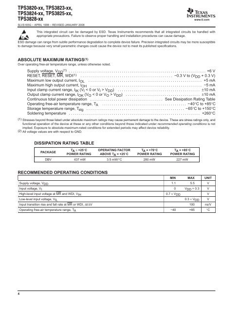
DISSIPATION RATING TABLE<br />
PACKAGE<br />
TA ≤ +25°C<br />
POWER RATING<br />
OPERATING FACTOR<br />
ABOVE TA = +25°C<br />
TA = +70°C<br />
POWER RATING<br />
TA = +85°C<br />
POWER RATING<br />
DBV 437 mW 3.5 mW/°C 280 mW 227 mW<br />
RECOMMENDED OPERATING CONDITIONS<br />
MIN MAX UNIT<br />
Supply voltage, VDD 1.1 5.5 V<br />
Input voltage, VI 0 VDD + 0.3 V<br />
High-level input voltage at MR and WDI, VIH 0.7 × VDD V<br />
Low-level input voltage, VIL 0.3 × VDD V<br />
Input transition rise and fall rate at MR or WDI, ∆t/∆V 100 ns/V<br />
Operating free-air temperature range, TA −40 +85 °C