Digital Image File Format and Storage - Video Preservation Website
Digital Image File Format and Storage - Video Preservation Website
Digital Image File Format and Storage - Video Preservation Website

Create successful ePaper yourself
Turn your PDF publications into a flip-book with our unique Google optimized e-Paper software.
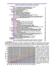
Film Grain, Resolution <strong>and</strong> Fundamental Film Particles<br />
Version 24 – August 2010<br />
Tim Vitale © 2010 use by permission only<br />
1 - Introduction<br />
Table 1: : Film Property vs Scale<br />
1<br />
2<br />
2 - Fundamental Film Particles – Silver-Halide 0.2 - 2.0 um<br />
Table 2: Feature ure Size <strong>and</strong> <strong>Digital</strong> Resolution<br />
Dye Clouds are the Fundamental <strong>Image</strong> Elements in Color Film<br />
3<br />
4<br />
6<br />
3 - Film Grain<br />
Dye Clouds in Color Film<br />
Film Grain in Black Black-<strong>and</strong>-White Film<br />
6<br />
6<br />
8<br />
Cross-Section Section of Film<br />
Grain Size Variability<br />
RMS Granularity – Film <strong>Image</strong> Noise not Film Grain Size<br />
9<br />
10<br />
10<br />
Table 3: RMS Granularit Granularity of Several Films<br />
Film Resolution – Sharpness<br />
System Resolving Power Equation<br />
111<br />
111<br />
113<br />
Lens Issues AAffecting<br />
Resolution<br />
Film Issues AAffecting<br />
Resolution<br />
Evaluating a Sy System: Camera, Lens <strong>and</strong> Film<br />
113<br />
113<br />
114<br />
Table 4: Selected Film & Lens Resolution Data<br />
Table 5: System em Resolving Power Data<br />
Measuring Film Grain<br />
114<br />
116<br />
117<br />
Print Grain Index<br />
Size of Film Grain: Example<br />
Table 6: Size Domains for Enlargement & Magnification<br />
117<br />
118<br />
118<br />
Table 7: Maximum Resolution of a Microscope<br />
4 - Eliminating ting Film Grain from an <strong>Image</strong><br />
Drum Scan Aperture<br />
118<br />
20<br />
221<br />
Art of Drum Scanning -- No Film Grain with Higher Resolution<br />
Table 8: Feature Size vs <strong>Digital</strong> Resolution vs Film<br />
Scan Resolution in Flatbed Scanning<br />
21<br />
222<br />
22<br />
Lens is the Limiting Factor for Flatbed Scanners<br />
Art of Flatbed Scanning<br />
Wet Mounting for Film Scanning<br />
223<br />
223<br />
223<br />
New Generation of Flatbed Scanners<br />
Next Generation of Scanners – Epson Perfection V750-M<br />
Software for Diminishing Film Grain<br />
224<br />
226<br />
227<br />
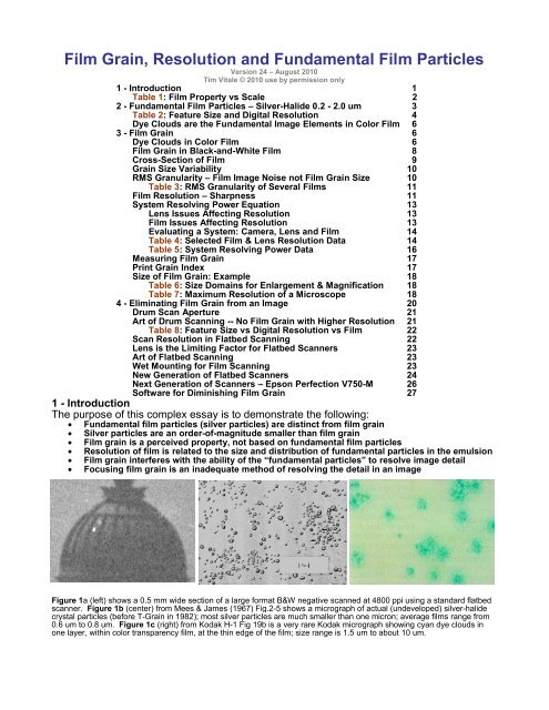
1 - Introduction<br />
The purpose of this complex essay is to demonstrate the following:<br />
<br />
<br />
Fundamental film particles (silver particles) are distinct from film grain<br />
Silver particles are an order-of of-magnitude smaller than film grain<br />
<br />
<br />
<br />
Film grain is a perceived property property, not based on fundamental film particles<br />
Resolution of film is related to the size <strong>and</strong> distribution of fundamental particles in the emulsion<br />
Film grain interferes with the ability of the “fundamen<br />
“fundamental tal particles” to resolve image detail<br />
Focusing film grain is an inadequate method of resolving the detail in an image<br />
Figure 1a (left) shows a 0.5 mm wide section of a large format B&W negative scanned at 4800 ppi using a st<strong>and</strong>ard flatbed<br />
scanner. Figure 1b (center) from Mees & James (1967) Fig.2 Fig.2-5 shows a micrograph of actual (undeveloped) silver-halide<br />
crystal particles (before T-Grain in 1982); ; mmost<br />
silver particles are much smaller than one micron; ; average films range from<br />
0.6 um to 0.8 um. Figure 1c (right) from Kodak HH-1<br />
Fig 19b is a very rare Kodak micrograph showing ing cyan dye clouds in<br />
one layer, within color transparency film, , at the thin edge of the film film; size range is 1.5 um to about 10 um.
tjvitale@ix.netcom.com 510-594-8277 8277 Tim Vitale © 2009 Use with permission only page 2<br />
The term “film grain” is often incorrectl incorrectly y used to describe the “fundamental” particles in a<br />
chemical-based based photographic image. Fundamental image particles are the smallest particles<br />
that form an image: (a) silver particles or (b) color dye clouds. It t can be seen in Figure 1a that<br />
detail is defined by the dark line of the dome rib against the gray panel; the film grain detracts<br />
from smoothness of the rib. In Fig Figure 24 (p24), , a wet <strong>and</strong> dry scan comparison of the sme<br />
image, , the effect is greater in the dry scan where the film grain is more pronou pronounced.<br />
Film grain rain is a repeating noise pattern that is an order of magnitude larger than the<br />
fundamental image particles. Film resolution is directly related to the size <strong>and</strong> distribution of<br />
silver particles in an emulsion. The noise pattern tends to obscure ure detail rather than define<br />
detail. The pattern is superimposed over the image image, , not the source of the image image.<br />
A common mistake is to think that film grain is the image-forming element. Many Kodak <strong>and</strong><br />
Fuji publications, including much of the popular pho photographic tographic literature (magazines),<br />
commonly make the mistake of referring to fundamental film particles as film grain. This<br />
further propagates the imprecise usage of the term.<br />
In the table below it can be seen that the size of film grain is often larger r than the ability of<br />
film to resolve detail of a specific ssize:<br />
10-30 microns (um) vs. 8 um. This strongly suggests<br />
that (a) film grain <strong>and</strong> (b) the ability to resolving detail are different properties.<br />
Table 1: Film Property vs Scale<br />
Size Domain I-------------------<br />
-------------------SCALE---------------------I Tool for<br />
What is<br />
Property Microns lp/mm ppi Evaluating Property Measured?<br />
Fundamental Particles 0.2-2.0 5000 5000-500 254,000-127,000 Microscopy Silver Particles<br />
Film Resolution* 8* 80* 4064* MTF Curve Resolving Power<br />
Film Grain 10-30 50-10 2540-1690 <strong>Image</strong> Enlargement Film Grain<br />
RMS Granularity 48** 10** 528** Microdensitometer Noise at 1.0D<br />
Graininess NA NA NA Print Grain Index R<strong>and</strong>om Film Noise<br />
Human Visual Acuity 85*** 6*** 300*** Human Vision Details<br />
* Applicable to Fuji Velvia RVP capable of 80 lp/mm native resolution.<br />
** Diameter of area used in the RMS Granularity measurement<br />
measurement; ; no units, a measure of image noise noise.<br />
*** Based on human not being able to resolve greater than 300 ppi.<br />
Film grain is a – perceived – visual phenomenon resulting from the visual accumulation of<br />
smaller particles through the thickness of the emulsion layer; see Film Grain, Section 3. The<br />
Kodak H1 publication says about film grain:<br />
“Although Although the viewer sees a granul granular pattern, , the eye is not necessarily seeing the individual<br />
silver particles, which range from about 0.002 mm down to about a tenth of that size size.”<br />
Experienced workers explain that different techniques such as (a) magnification (through a<br />
microscope or loupe), (b) enlargement (photographic print) <strong>and</strong> (c) scanning, yield different<br />
results for film grain size. These findings, in themselves, are highly suggestive that film grain<br />
is a perceived property that depend depends on the conditions of examination.<br />
Working with Film Grain<br />
In an era of 4800-6400 00 ppi flatbeds, one of the remaining claims to superiority of the drum<br />
scanner is its ability to “tune” the capture system to the physical image structure of specific<br />
films using two parameters: aperture <strong>and</strong> pitch. Many activities of the drum scan operator<br />
are geared towards eliminating film grain while maintaining resolution. The resulting drum drumscanned<br />
image is prized when it looks like a digital image free of film grain.<br />
On the other h<strong>and</strong>, when creating a print with film using an enlarger (analog<br />
technique), operators often use a grain-magnifying tool to assure the<br />
sharp focus of film. Figure 2 shows a Micro-Sight 12x grain focusing tool.<br />
From this action, some operators have assumed that creating sharp “film<br />
grain” is the key to achieving image sharpness. However, film grain is not<br />
actually tually sharp because it is made up of numerous smaller particles that are<br />
an order-of-magnitude magnitude smaller than the film grain, composited through the<br />
thickness of the emulsion.<br />
Figure 2
tjvitale@ix.netcom.com 510-594-8277 Tim Vitale © 2009 Use with permission only page 3<br />
The problems of (1) locating a well-focused region of a small piece of film in a 35 mm film<br />
frame (24 x 36 mm), (2) evaluating its degree of focus <strong>and</strong> then (3) focusing that region of the<br />
film, explains why “focusing the grain” has become a common default for determining<br />
image sharpness. Focusing on the perceived film grain is a misapplication of imaging<br />
resources, because film grain has indistinct edges. It is image noise not “grain.”<br />
Achieving fine detail with crisp contrast differences should be the goal of the imaging<br />
process, be it on a flatbed or drum scanner. Based on the generic information in an MTF<br />
Curve, focus is a function maximizing contrast between lights <strong>and</strong> darks.<br />
Good focus is achieved by finding the highest degree of contrast difference between light <strong>and</strong><br />
dark, in a bit of blurry detail, while avoiding the use of film grain. In the original scene, the<br />
detail could have been black <strong>and</strong> white before they were transformed to lower-contrast grays<br />
by the lens <strong>and</strong> then diffused by the silver particles or dye clouds in the film.<br />
2 - Fundamental Film Particles – Silver-Halide Crystals<br />
The fundamental image particles in chemical-based images are:<br />
Silver particles in B&W images<br />
Color dye clouds in color film images (clouds develop around silver particle centers)<br />
Silver-halide particles (in undeveloped film) average about 0.2 - 2.0 microns (one micron<br />
equals one millionth of a meter or, a thous<strong>and</strong>th of a millimeter). Color dye clouds range<br />
from 1.0 um to 10 um.<br />
Silver-halide crystals are 0.2- 2.0 um<br />
Color dye clouds are 1.0 to 6-10 um<br />
Human vision is orders-of-magnitude less acute than the size of the silver particles. Even<br />
corrected, human vision ranges from 75-100 microns, with an average of 84 um, or 300 dpi.<br />
Using a common 10x loupe, humans can image 7.5 to 10 um, which is still too coarse to see<br />
individual silver particles, even at a thin edge of an image.<br />
The fundamental image particles (silver), when rescaled into dimensions commonly used for<br />
the wavelengths of visible light, range from 200 to 2000 nm (nanometers).<br />
1" = 25.4 mm (millimeters)<br />
1" = 25,400 um (microns)<br />
1” = 25,400,000 nm (nanometers)<br />
1000 microns (um) = 1 mm<br />
1000000 microns = 1 meter<br />
1000 nm = 1 micron (um)<br />
1000000 nm = 1 mm<br />
1000000000 nanometers (nm) = 1 meter<br />
The size domain of visible light is 400-750nm; blue light ranges from 380-450 nm; green light<br />
ranges 450-550 nm; <strong>and</strong> red light ranges 550-750 nm. Ultra-violet light ranges 205-380 nm,<br />
while infrared radiation ranges 750-5000 nm. Note that the smallest silver particles (0.2-0.8<br />
microns) are not visible unless clumped into larger agglomerates, because most are smaller<br />
than the wavelengths of light.<br />
The light microscope has a theoretical maximum resolution of 1000X when using an oil<br />
immersion objective <strong>and</strong> condenser. With a 100x oil immersion lens <strong>and</strong> a 1.25 NA oil<br />
immersion Abbe-type condenser, a microscope can resolve particles at 250nm, or 0.25 um.<br />
They can be used to see fundamental film particles; see details on p 18. A microscope<br />
cannot be used to see film grain because the closer one gets, the more indistinct the<br />
apparent edges of the perceived particles become because film grain is noise not particles.
tjvitale@ix.netcom.com 510-594-8277 Tim Vitale © 2009 Use with permission only page 4<br />
Figure 3: KODAK T-GRAIN emulsion Figure 4: Conventional silver-halide<br />
crystals 1982-present, H-1 crystals, 1860-1982, H-1<br />
Quoted directly from the Kodak Motion Picture Publication H-1 (1999):<br />
“Incorporating T-GRAIN Emulsions into films improves film speed without sacrificing fine grain. The<br />
uniquely shaped grains align better than conventional silver crystals, absorbing <strong>and</strong> transmitting light more<br />
effectively. In recent years, [first in Kodacolor VR, 1982] a new type of emulsion KODAK T-GRAIN® was<br />
incorporated into some Kodak films. The amount of exposure, which determines the densities of various<br />
areas, also affects the graininess of all films. Other factors that affect graininess are different developers<br />
<strong>and</strong> different amounts of development time of black-<strong>and</strong>-white films. Because the development processes<br />
of color films are rigidly fixed, the effect of development [on them] is rarely a factor in their graininess<br />
(however, forced processing does cause an increase in graininess). Because many color films are made<br />
with emulsion layers of varying graininess levels, increasing the exposure (up to a point) places more of the<br />
density in the finer-grained layers, which actually reduces the overall graininess of the observed images.”<br />
Table 2: Feature Size versus <strong>Digital</strong> Resolution<br />
Size <strong>Digital</strong> Resolution Imaging Device<br />
0.1 um 254,000 ppi SEM/XRD<br />
0.2 um 127,000 ppi SEM/XRD<br />
0.5 um 50,800 ppi SEM/XRD<br />
0.8 um 31,750 ppi SEM/XRD<br />
1.0 um 25,400 ppi Light Microscope<br />
2.0 um 12,700 ppi Light Microscope<br />
3.0 um 8,467 ppi Light Microscope<br />
4.0 um 6,350 ppi Light Microscope<br />
5.0 um 5,080 ppi Light Microscope & Scanners<br />
5.3 um 4,800 ppi Drum or Flatbed Scanners<br />
5.5 um 4,618 ppi Drum or Flatbed Scanners<br />
6.0 um 4,233 ppi Drum or Flatbed Scanners<br />
6.34 um 4,000 ppi Drum or Flatbed Scanners<br />
7.0 um 3,629 ppi Drum or Flatbed Scanners<br />
8.0 um 3,175 ppi Drum or Flatbed Scanners<br />
8.5 um 3,000 ppi Drum or Flatbed Scanners<br />
9.0 um 2,822 ppi Drum or Flatbed Scanners<br />
10.0 um 2,540 ppi Drum or Flatbed Scanners<br />
10.5 um 2,400 ppi Drum or Flatbed Scanners<br />
12.0 um 2,117 ppi Drum or Flatbed Scanners<br />
13.0 um 1,954 ppi Drum or Flatbed Scanners<br />
15.0 um 1,693 ppi Drum or Flatbed Scanners<br />
20.0 um 1,270 ppi Drum or Flatbed Scanners<br />
21.2 um 1,200 ppi Drum or Flatbed Scanners<br />
25.0 um 1,016 ppi Drum or Flatbed Scanners<br />
50.0 um 508 ppi Drum or Flatbed Scanners<br />
60.0 um 423 ppi Young Human Eyes<br />
75.0 um 340 ppi Above Average Human Eyes<br />
85.0 um 300 ppi Average Human Eyes<br />
100 um 254 ppi Most Human Eyes<br />
1000 um 25.4 ppi One Millimeter<br />
1000000 um NA One Meter<br />
In The Theory of the Photographic Process, eds: C.E.K. Mees <strong>and</strong> J.T. James (1967, 3rd),<br />
Chapter 2 by C.R. Berry <strong>and</strong> R.P. Lovel<strong>and</strong>, pp 38-40 they list the average silver-halide<br />
particle sizes for film emulsions such as: high-resolution film, motion picture film, portrait film
tjvitale@ix.netcom.com 510-594-8277 8277 Tim Vitale © 2009 Use with permission only page 5<br />
<strong>and</strong> high-speed speed film. The size range is from 0.30 to 1.71 um (microns), about the size of<br />
those listed in the Kodak H-1 publication, 0.2 to 2.0 um.<br />
Figure 5: Figure labeled 2.7 was taken from Mees <strong>and</strong> James (1967) p 39.<br />
Figures 6-9: : <strong>Image</strong>s labeled “Figures 2.4, 2.5 <strong>and</strong> 2.6” are from Mees & James (1967) pp 35-39 39, all have 1um<br />
markers. The image labeled “Figure re 1” is from Baines (1976) The Science of Photography, , p112.
tjvitale@ix.netcom.com 510-594-8277 8277 Tim Vitale © 2009 Use with permission only page 6<br />
Dye Clouds are the Fundamental <strong>Image</strong> Elements in Color Film<br />
Color films have dye clouds (1.0 1.0 - 10 microns [um] across) that start from silver particle, or<br />
clumps, core(s). The dye clouds devel develop around the silver particle’s or clumps of particles:<br />
see below. Color films have lower resolution than B&W films, because the fundamental<br />
particle size is larger than in B&W film.<br />
Figure 10: From Kodak Publication H-1: 1: The image on the le left ft in a representation of the mix silver particle sizes<br />
found in B&W films, before T-Grain. Grain. The center image shows cyan dye clouds with silver particle clump(s)<br />
centers. On the right, the dye clouds are shown after full development, including a competing dye coupler,<br />
which reduces dye cloud size. In actual film, the ddye<br />
clouds overlap within layers. In modern color films there<br />
are up to 9 layers of dye clouds; three sub sub-layers in each of the 3 colors of dye.<br />
The Kodak H-1 Publication shows discretely developed dye clouds to be about 1.0 um to 6-<br />
10 um (microns) across. This assumes that the core silver particle is either a clump of<br />
particles about 0.4 to 2.0 um across, or an individual silver particle about 0.4 - 0.8 um in<br />
width. The images above were e made from edges of areas of very faint color, <strong>and</strong> are<br />
probably from a slow speed film. . In areas of greater density individual dye clouds cannot be<br />
distinguished, , however there is the modulation of tone called “film grain grain.” Each color layer<br />
group can have three different light response speeds speeds: : (1) a fine grain “slow” layer, (2) a<br />
moderate grain “normal” speed layer <strong>and</strong> (3) a coarse grain “fast” layer.<br />
3 - Film Grain<br />
Film grain is the product of the human eye a<strong>and</strong><br />
nd brain working in combination when viewing<br />
very large numbers fundamental image particles, seen through the full thickness of the<br />
emulsion layer, often composed of numerous sub-layers. Film ilm grain is “perce “perceived” as “fuzzy”<br />
particles just beyond the ability of our human eyes to resolve, rather than an actual physical<br />
“particle.” Film Grain is a real visual phenomenon created by the interaction of the human<br />
eye <strong>and</strong> brain with the noise in film film. Film grain influences the sharpness of a film by acting<br />
as a regular noise pattern (unwanted image info information) that diminishes the ability to resolve<br />
image detail at the size domain of the “perceived” film grain.<br />
Seeing film grain requires the brain to cluster noise into the appearance of clumps clumps. Some<br />
magnification will help see grain in an image that aappears<br />
ppears to have a smooth tone, see Fig 11.<br />
However, applying greater magnification does not resolve grain because it is indistinct.<br />
Figure 11 (top half): : Film grain from Kodak HH-1,<br />
p28
tjvitale@ix.netcom.com 510-594-8277 Tim Vitale © 2009 Use with permission only page 7<br />
Figure 11 (bottom half): Film grain from Kodak H-1, p28<br />
Dye Clouds in Color Film<br />
Dye clouds are the source of film grain in color films. Dye clouds range in size from 1.0 um<br />
to 6 um, <strong>and</strong> up to 10 microns across when in small clumps. There are up to 9 layers of dye<br />
clouds in modern color film (see Fig.12), thus the perception film grain is made through the<br />
thickness of the 9 dye layers of the image emulsion. Color films have lower resolution than<br />
B&W films, because the smallest image components are larger than in B&W film.<br />
Transparency films are said to be grainless because there are no silver particles in the final<br />
emulsion, <strong>and</strong> the dye clouds have indistinct edges. While silver particle are present in color<br />
film before <strong>and</strong> during the many stages of the development process, they are bleached out<br />
near the end of processing. The complexity of the silver-to-dye transition during development<br />
<strong>and</strong> filamentation of dye cloud, through the multiple emulsion layers, means that only rare<br />
“single dye cloud” will ever be observed. Mostly, single dye clouds will be found at edges,<br />
<strong>and</strong> in thin image areas of a pure color that is equivalent to a dye (CMY), such as in the<br />
Kodak (H-1, Fig 13a-d) images below.<br />
Film Grain in a color film is the accumulation of tens, to hundreds, of dye clouds in each of<br />
the nine dye layers found in modern color film. Fuji film data sheets from 1986 show 6 layers<br />
in Fujichrome professional 400 D (RHP); <strong>and</strong> 7 layers in Fujichrome professional (sheet film)<br />
50D RFP, 64T RTP <strong>and</strong> 100D RDP.<br />
Figure 12: Nine layers of CMY color dyes found in Fuji Provia 400 (2007)<br />
. Similar color Fuji films from 1980-90 had 6, 7<br />
<strong>and</strong> 8 layers.
tjvitale@ix.netcom.com 510-594-8277 Tim Vitale © 2009 Use with permission only page 8<br />
Figure 13a-d: <strong>Image</strong>s from Kodak H-1 (1998) Fig. 19, p25. Photomicrographs at 1200x of a cyan dye layer made very<br />
thin to show structure. From upper left to lower right: (a) the film after color development showing clumps of metallic<br />
silver grains (0.4 to 1.0 um) surrounded by dye clouds (1-10 um); (b) the same film developed with a completing coupler<br />
that reduces the size of the dye clouds, reducing the grain size; (c) the same film developed without a competing dye<br />
coupler, after bleaching; <strong>and</strong> (d) developed with a competing dye coupler after silver bleaching; dye cloud size is as<br />
small as 1.0 um.<br />
Film Grain in Black-<strong>and</strong>-White Film<br />
B&W film is composed of numerous silver particles which are an order of magnitude (ten<br />
times) smaller than the size domain of film grain size. Silver particles range in size from 0.2<br />
um to 2.0 um, with an average size of 0.6 um, while film grain appears to ranges in size from<br />
6 um to 30 um. Film grain is so indistinct it is difficult to measure; a range of 8-12 um is<br />
thought to be average by many workers.<br />
Film grain size is not measured using RMS Granularity, which is a unitless evaluation of<br />
unevenness of a uniform tone. RMS Granularity has no units.<br />
From Kodak’s Kodak Professional Black-<strong>and</strong> White Films, Pub. F-5 (1984) on p 28:<br />
“Graininess: The densities in black-<strong>and</strong>-white negatives are composed of microscopic grains of<br />
black metallic silver. By their r<strong>and</strong>om placement in the gelatin of the emulsion, there is a statical<br />
clumping of the grains that form the familiar granular pattern that becomes visible when a<br />
negative is enlarged enough. ”<br />
Same, <strong>and</strong> on p 32:<br />
“While commonly called the emulsion, the light-sensitive layer of a film is actually a suspension<br />
of silver halide crystals in gelatin. The size <strong>and</strong> distribution of the crystals, the types of halides<br />
of which the crystal are made, their number, how they have been sensitized during manufacture,<br />
<strong>and</strong> the thickness of the emulsion layer, along with many controlling steps in the emulsion <strong>and</strong><br />
film manufacture, determine such film characteristics as speed, contrast, characteristic curve<br />
shape, graininess, resolving power, <strong>and</strong> optical sensitivity.”<br />
In Kodak publication on motion picture film Publication H-1 (1999) p 25:<br />
“One might expect a photographic image made up of cyan, magenta, <strong>and</strong> yellow dye clouds to<br />
appear more grainy than the corresponding silver image. In fact, close to its resolution limit [6<br />
lp/mm, 300 ppi], the eye sees only brightness differences <strong>and</strong> does not distinguish color in very<br />
small detail. When color films are projected, the “dye-cloud clusters” form groups similar to<br />
“silver-grain clusters” in black-<strong>and</strong>-white films. At high magnifications, these clusters cause the<br />
appearance of graininess in the projected screen image.”
tjvitale@ix.netcom.com 510-594-8277 Tim Vitale © 2009 Use with permission only page 9<br />
Figure 14: From Kodak Professional Black-<strong>and</strong> White Films (1998) p 33.<br />
On p 32: “The densities in black-<strong>and</strong>white<br />
negatives are composed of<br />
microscopic grains of metallic silver.<br />
Because the grains are placed<br />
r<strong>and</strong>omly in the gelatin emulsion,<br />
[visual] clumping occurs <strong>and</strong> forms the<br />
familiar granular [film grain] pattern that<br />
becomes increasingly visible as<br />
negatives are enlarged to greater<br />
degrees.<br />
As a rule, the faster the film, the<br />
greater the tendency towards<br />
graininess. Kodak T-Max Professional<br />
films, however, bend this rule.<br />
Because these films have Kodak T-<br />
Grain Emulsion, they have finer grain<br />
than conventional films of comparable<br />
speed.”<br />
On p 33: “The type of developer you<br />
use affects graininess. A fine grain<br />
developer decreases graininess,<br />
usually with some loss in speed.<br />
Overdevelopment, i.e., using <strong>and</strong><br />
extended development time, a high<br />
temperature, or a highly active<br />
developer, increases graininess.<br />
High density [produced] by<br />
overexposure of a negative also<br />
increases graininess. Proper<br />
exposure <strong>and</strong> development almost<br />
always produce an optimum level of<br />
graininess. (Large, even-toned areas<br />
in the mid-tones of a photograph will<br />
appear more grainy than dark- or lighttoned<br />
areas or areas that include fine<br />
detail.)”<br />
On p 32: “The ability of a film to<br />
record fine detail is called definition,<br />
which is a composite of granularity,<br />
resolving power, <strong>and</strong> sharpness. The<br />
measurement of this characteristic is<br />
called resolving power or resolution.<br />
The visual effect of unevenness in<br />
areas that should be uniform is called<br />
graininess. An objective measurement<br />
of graininess is call granularity.<br />
[Referred to as RMS Granularity <strong>and</strong><br />
Noise in this essay]<br />
On p 34: “The sharpness of a film is<br />
the subjective perception of good<br />
edge distinction between details in a<br />
photograph.<br />
Film manufacturers …measure this<br />
using a sine-wave test pattern<br />
…recorded on film…<strong>and</strong> scanned by<br />
sensitive measuring equipment.<br />
[Called an MTF Curve]
tjvitale@ix.netcom.com 510-594-8277 8277 Tim Vitale © 2009 Use with permission only page 10<br />
On the previous page are several images of the same subject shot oon<br />
different film films showing<br />
increasing “graininess” in the series from top to bottom. The images were taken from Kodak<br />
Professional Black-<strong>and</strong>-White White Films Films, Pub F-5 (1998) p 33. The quotes on the right were<br />
pulled from pp 32-34 in the same publication.<br />
Cross-Section of Film<br />
While microscopic images of discrete silver particles can be made under special<br />
circumstances, the thickness of silver silver-halide-gelatin gelatin emulsion has tens, to hundred hundreds, of silver<br />
particle stacked on one another in a small region. Even if human vision was more acute,<br />
individual particles could not be resolved because they are too close to each other when<br />
observed through the he thickness of the emulsion.<br />
Figure 15: On the left: Figure 46 from Kodak H1, is a cross-section section of a Kodak color negative film, the film is 0.075”<br />
thick, each dye layer is 0.003” thick. On the right: is a cross-section section diagram from Sams Publication, Film Basics for<br />
<strong>Digital</strong> Photographers by John Upton, Joseph Ciaglia, Peter Kuhns & Barbara London: Ch 4, June 2004 2004, it can be<br />
seen that individual silver particles would be difficult to resolve within the emulsion layer.<br />
Grain Size Variability<br />
Grain size is highly dependent on exposur exposure <strong>and</strong> development. In general, higher<br />
temperature favors larger grain; ; llonger<br />
onger development time favors larger film grain size size; <strong>and</strong><br />
specific developers produced larger or smaller grain depending on aggressiveness <strong>and</strong> pH.<br />
Short exposures use the larger more sensitive silver-halide halide particles in the film, creating an<br />
image with larger film grain for a quick exposure.<br />
Most films have low, medium <strong>and</strong> fast light sensitive layers, based mostly on silver-halide<br />
particle size. Film grain size, therefore therefore, will vary from image to image but will probably stay<br />
within a range based on the specific film emulsion being exposed.<br />
RMS Granularity – Measure of Film Noise not Film Grain Size<br />
RMS Granularity measures the noise in film film. The protocol measures the variation of tone in<br />
an area of uniform density (usually 1.0D) 1.0D). RMS Granularity is not a measure of “graininess,”<br />
even though several publications have made this mistake.<br />
RMS Granularity is s a measure of the variability of an area of uniform film density density, using a<br />
densitometer, through a 48 um aperture .<br />
The 48 um measurement ment aperture is much larger than actual silver particles or perceived film<br />
grain, so it can only measure the variability of film density. The variability of the measured<br />
region, which is ideally uniform, iis<br />
called noise. RMS Granularity is a measure of film noise.<br />
RMS Granularity numbers range from 55-50<br />
<strong>and</strong> they have no units. The lower the RMS<br />
Granularity number the lower the noise in a specific film. Measurements without units are<br />
relative to the measurement.
tjvitale@ix.netcom.com 510-594-8277 Tim Vitale © 2009 Use with permission only page 11<br />
Figure 16: Measuring a RMS Granularity using a 48-micron sample area. Root Mean Square is the St<strong>and</strong>ard<br />
Deviation of the Mean of the range of density measurements made on 1.0 D film. <strong>Image</strong> is from Kodak H-1(1999) p24.<br />
After about 1980, film manufactures began measuring film “granularity” using the RMS<br />
Granularity protocol. Kodak slide films have a RMS Granularity of between 8 <strong>and</strong> 13 <strong>and</strong> Fuji<br />
reversal films have values between 7 <strong>and</strong> 10. [Remember: no units, not a measure of grain<br />
size.] Some color negative films have RMS Granularity rating of 5, as noise free as film can<br />
achieve. However, negative film must be printed, therefore the overall RMS Granularity of<br />
the system is much higher because it is combined with the grain of the print.<br />
Table 3: RMS Granularity of Several Films with their Native Resolution<br />
Film Name RMS Native Resolution Native Resolution<br />
Granularity* lp/mm @ 30% ppi @ 30%<br />
Kodak PORTRA 160NC NA 73 3708<br />
Kodak ULTRA 100UC NA 60 3050<br />
Kodak EDUPE 8.7 60 3050<br />
Kodachrome 25 9 50 2540<br />
Kodachrome 64 10 50 2540<br />
Ektachrome 5071 (dup) 9 50 2540<br />
Ektachrome 50 13 40 2030<br />
Ektachrome 64 12 40 2030<br />
Ektachrome 100 11 45 2290<br />
Ektachrome 100GX 8 60 3050<br />
Ektachrome 100plus EPP 11 45 2290<br />
Ektachrome 160 13 35 1780<br />
Fuji Velvia 50 RVP 8 80 4064<br />
Fuji Velvia 100 RVP100F 8 80 3300<br />
Fuji Provia 100F RPD 9 55 2800<br />
Fuji Astra 100 RAP 10 45 2290<br />
Fuji Astra 100F RAP100F 7 65 3300<br />
Fujichrome EI 100 10 45 2290<br />
Average 9.8 64.3 3264<br />
Film Resolution - Sharpness<br />
Film Resolution defines the potential resolving power of a film; Kodak calls this sharpness.<br />
Herein, it is referred to the “native” resolution of film. Native resolution is determined from<br />
manufacture-published MTF Curves, which are found in the film data sheets. The MTF<br />
Curve is measured using a sine wave bar (see below) that is contact printed directly onto the<br />
film without using a lens; each measurement required about 2 weeks by manufacturer<br />
technicians. [Note: sharpness is determined herein at 30% contrast (% Response).]<br />
In reality the resolution of film involves using a camera lens. Thus, true evaluation of film<br />
resolution must use the Resolving Power Equation (p 13). Both Kodak <strong>and</strong> Fuji have their<br />
own versions of the equation. When a lens is in the system (camera), the resolution of the<br />
film is about 30% to 80% of native resolution. It can be said that the greater the "native"<br />
resolution of the film, the greater the loss of the resolution in the system due to the use of a<br />
lens. The loss of system resolution is due to image deterioration by (1) exposed through a<br />
lens, (2) variables in film transport <strong>and</strong> (3) film processing. This evaluation is covered in<br />
great detail in another essay by the author held in the AIC-EMG Library<br />
, see “<strong>Image</strong> <strong>File</strong> <strong>Format</strong>s: TIFF, JPEG & JPEG2000.”
tjvitale@ix.netcom.com 510-594-8277 8277 Tim Vitale © 2009 Use with permission only page 12<br />
Figure 17: : The images labeled “Figures 34 & 35” are from Kodak HH-1<br />
(1999) p 38. Fig. 34 4 shows an exam example of<br />
the decreasing sine wave object used for determining MTF data. In Fig. 35 plot line A shows edge edge-contrast<br />
sharpening while plot B shows no edge sharpening effect effect. In the lower two MTF Curves, taken from Kodak film<br />
data sheets, examples depict both A & B behavior behaviors. Lower row on the left, is the MFT Curve for Kodachrome 200<br />
(PKL); it shows edge enhancement ement with a direct direct-contact, the MTF value at 30% contrast difference (y axis) is 50lp/mm,<br />
or 2540 ppi digital equivalent. . OOn<br />
the right, the MTF Curve from Kodak PORTRA 160NC color negative film<br />
that has only slight edge enhancement ment with a native resolution at 30% contrast difference of 63-lp/mm lp/mm, or 3200 ppi<br />
digital equivalent. Note that both MTF Curves turn down (sharp decrease in resolution) at about 20 lp/mm (25 um),<br />
the possible influence of film grain on film resolution.<br />
The MTF Curve of Kodachrome 200 (PKL) transparency film shows a native resolution of 50 50lp/mm,<br />
(2540 ppi digital equivalent equivalent). . Using the Fuji Resolving Power Equati Equation [EQ2, below],<br />
PKL film shot through an excellent llent 35mm format lens (100 lp/mm lens) will have a final<br />
resolution of 33-lp/mm, with a digital equivalent resolution of 1962 ppi ppi; a loss of 34% from the<br />
native MTF data.
tjvitale@ix.netcom.com 510-594-8277 Tim Vitale © 2009 Use with permission only page 13<br />
Note the convention used herein: apply the “digital equivalent” units of ppi (pixels per inch)<br />
to analog film. Film is an analog media; the units of lp/mm (line pairs per millimeter) are best<br />
applied when describing its resolution. However, expediency when comparing between the<br />
analog <strong>and</strong> digital domains is enhanced by applying the same units to both.<br />
The Kodak PORTRA 160NC color negative film’s MTF Curve (lower right in Fig 17) shows a<br />
resolution of 73 lp/mm for the red dye at 30% contrast (% Response) or 3680 ppi digital<br />
equivalent. The blue <strong>and</strong> green dye layers have higher contrast at 73 lp/mm, but the red dye<br />
value is used here. When 160NC film is run through the Fuji Resolving Power Equation<br />
[EQ2, below], using an excellent 35mm format lens (100 lp/mm lens) the final resolution of<br />
the system is 42-lp/mm (2143 ppi digital equivalent) a loss of 42%, from the native MTF data<br />
at 30% contrast.<br />
System Resolving Power Equation<br />
There are many factors rolled onto the system resolving power equations. A "system" is the<br />
whole photographic unit, (a) camera [lens to film alignment], (b) lens [resolution <strong>and</strong> color<br />
shift], (c) film <strong>and</strong> (d) processing.<br />
In the following equations, one term (1/r) is for the film <strong>and</strong> other(s) are for the lens(es). The<br />
resolving power for a “print” system (EQ1) includes terms for an enlarging lens <strong>and</strong> the<br />
resolution of the paper the equation, lowering the overall image resolution profoundly.<br />
EQ1: 1/R = 1/r [film] + 1/r [camera lens] + 1/r [enlarging lens] + 1/r [printing paper]<br />
The FujiFilm Resolving Power for a simple camera <strong>and</strong> film system (EQ2) such as for<br />
creating transparencies (slides) can be found in the Fuji Data Guide (p102, 1998):<br />
EQ2: 1/R [system] = 1/r [film] + 1/r [lens]<br />
Where: (1) R = overall resolving power, <strong>and</strong> (2) r = resolving power of each component<br />
Kodak uses the following equation, EQ3, in its data sheets <strong>and</strong> h<strong>and</strong>books. It is more<br />
complicated, where each term is squared, but yields almost the same results. It is NOT<br />
used in Table 5 or other arguments in this essay.<br />
EQ3: 1/R 2 [system] = 1/r 2 [film] + 1/r 2 [lens]<br />
Lens Issues Affecting Resolution<br />
There are at least 7 different types of lens aberrations:<br />
Chromatic aberration<br />
Spherical aberration<br />
Coma (uneven magnification)<br />
Astigmatism (non-flat focus)<br />
Flare (external light scattering)<br />
Dispersion (internal light scattering)<br />
Misaligned lens elements<br />
The center of the lens is generally the sharpest. Resolution declines towards the edge of the<br />
image circle. Good modern lenses are not capable of more than 80-120 line-pairs per<br />
millimeter (lp/mm) at the center of the lens, <strong>and</strong> much less, towards the edges. Wide<br />
apertures compromise image quality dramatically because the light goes through most of the<br />
glass in the lens. Low f-stops (f3.5 to f5.6) in large format lenses are only capable of 10-20<br />
lp/mm at the edges wide open <strong>and</strong> chromatic aberrations can be extreme - producing a<br />
rainbow of colors on large high-contrast features (black line on white) near the edges, where<br />
the various colors in light focus in different locations.<br />
Film Issues Affecting Resolution<br />
The problems with film have been described in detail within many online publications.<br />
Achieving crisp focus is the principal problem. However, keeping the film flat in any camera,<br />
<strong>and</strong> perpendicular to the lens axis is the critical issue. This is especially critical in film holders<br />
with large format view cameras. The next most critical issues are the variants in temperature
tjvitale@ix.netcom.com 510-594-8277 Tim Vitale © 2009 Use with permission only page 14<br />
<strong>and</strong> humidity through the life of the film <strong>and</strong> time period between exposure <strong>and</strong> processing.<br />
The issues forming an image on film include:<br />
Goodness of focus<br />
Trueness of lens axis to film axis<br />
Warp of the film in the film holder or film path<br />
Aperture size (f-stop)<br />
Shutter Speed<br />
Vibration in all phases<br />
Dirt <strong>and</strong> haze on lens (light scatter)<br />
Film developing variables (exhaustion, impure water or impure chemicals)<br />
Heat <strong>and</strong> humidity in storage before <strong>and</strong> after exposure <strong>and</strong> processing<br />
Time since exposure <strong>and</strong> possible exposure to x-rays during airport screening<br />
The exposure parameters of shutter speed <strong>and</strong> f-stop effect sharpness markedly. The fstops<br />
above <strong>and</strong> below the optimal lens iris opening, of f5.6 to f8, degrade the image<br />
noticeably. Slow shutter speeds allow for h<strong>and</strong>-induced shake during exposure decreasing<br />
image sharpness. Fast shutter speeds require longer processing times which enlarges film<br />
silver particle size, decreasing film resolution. A short exposure self-selects the more<br />
sensitive silver particle, which happens to be the larger silver particles. Mirror travel followed<br />
by an abrupt stop in SLRs can have an affect on camera movement (even while on a tripod)<br />
when using faster shutter speeds where the early period of "shake" is a relatively large<br />
portion of the full exposure time.<br />
Evaluating a System: Camera, Lens <strong>and</strong> Film<br />
Using the photographic system “Resolving Power Equation” EQ2 (above) from FujiFilm<br />
Professional Data Guide AF3-141E (2002) p 129; <strong>and</strong> the film resolution data in Table 4<br />
below, the results are reported in Table 5, on the following page.<br />
Table 4: Selected Film <strong>and</strong> Lens Resolution Data<br />
Native Film Resolution in ppi<br />
Film Resolution 1/r [film] No Lens in Path at 30% Contrast<br />
Kodak Ektachrome 160 35 lp/mm 0.0286 1778<br />
Fuji Astia RAP 45 lp/mm 0.022 2286<br />
Fuji Provia 100F RDP 55 lp/mm 0.0182 2794<br />
Kodak Ektachrome 100GX 60 lp/mm 0.0167 3050<br />
Kodak Tri-X 400 (2004) 65 lp/mm 0.0154 3302<br />
Fuji Velvia RVP 80 lp/mm 0.0125 4064<br />
Kodak Portra 160NC Color Neg 80 lp/mm 0.0125 4064<br />
Kodak Plus-X 125 (2006) 80 lp/mm 0.0125 4064<br />
Kodak VR100 Color Neg 100 lp/mm 0.0100 5080<br />
Kodak Technical Pan (2004) 142 lp/mm 0.007 7214<br />
Kodak Panatomic-X 170 lp/mm 0.0059 8636<br />
Lens Resolution 1/r [lens] Lens Cost<br />
Old lens (1840-1930) & LF lens 20 lp/mm 0.05 $50-1500<br />
Average lens 40 lp/mm 0.025 $150-500<br />
Very Good LF lens 60 lp/mm 0.0167 $300-800*<br />
Excellent LF lens 80 lp/mm 0.0125 $1000-3000**<br />
Superior 35 mm format lens 100 lp/mm 0.01 $350-5000***<br />
Outst<strong>and</strong>ing 35 mm lens 120 lp/mm 0.0083 $350-1000§<br />
Exceptional 35mm lens 140 lp/mm 0.0071 $350-1000Δ<br />
Best Possible 35mm lens 200 lp/mm 0.005 you won’t find one<br />
Vapor-ware lens 600 lp/mm 0.00167 you’ll hear about it, but you can’t find one<br />
* Many 35 mm, medium format <strong>and</strong> large format lenses at f8; or better lenses at f11 or f16.<br />
** Schneider 150 APO Symmar f5.6 at f8.<br />
*** Many second-tier lenses at f8.<br />
§ Nikkor & Canon 50mm & 85mm lenses at f8, on a tripod, superior processing, film only, no prints.<br />
Δ Leica or Zeiss 35 mm or medium format lenses.<br />
In the film <strong>and</strong> lens systems described below, the image is dramatically degraded by all lens<br />
<strong>and</strong> film issues described above (p 13-14). Loss of image quality ranges from 23-90% of<br />
native MTF resolution. Fixed cameras, such as 35 mm rangefinders <strong>and</strong> SLR bodies, <strong>and</strong>,<br />
medium format (MF), 2¼ x 2¼, or 6 x 6 cm <strong>and</strong> 2¼ x 2¾, or 6 x 7 cm, have fairly flat film<br />
planes <strong>and</strong> rigidly fixed lens-to-film axis.
tjvitale@ix.netcom.com 510-594-8277 Tim Vitale © 2009 Use with permission only page 15<br />
Large format (LF) cameras use film holders that do not have flat film planes. Large film (8 x<br />
10) can sag <strong>and</strong> the center of all sizes can have a slight warp. The lens-to-film axis in a view<br />
camera is never fixed <strong>and</strong> needs to be aligned at each setup. The Zigalign tool is commonly<br />
used by view camera operators to assure perfect alignment between lens <strong>and</strong> image plane.<br />
In digital cameras the media is never warped or out of plane unless manufactured poorly.<br />
Figure 18 shows the effect of lens quality on specific films found in the Table 4. Selected<br />
modern films are processed through EQ2 using hypothetical lenses of various resolving<br />
capabilities:<br />
average (40 lp/mm)<br />
good (60 lp/mm)<br />
very good (80 lp/mm)<br />
excellent (100 lp/mm)<br />
superior (120 lp/mm)<br />
Figure 18: The graph shows the effects of lens quality on films with increasing native resolution (more acute curve).<br />
The data points on the curve are the System Resolution calculations for the combination of film <strong>and</strong> lens; see Table 5<br />
for details. The higher the native resolution of the film the more it is affected by the lens.<br />
Table 5 (next page) shows the incremental effects of (a) lens issues <strong>and</strong> (b) film issues on<br />
the final resolution of a system (camera) using the Fuji Resolving Power Equation [EQ 2].<br />
The modern films listed in Table 4 are processed through EQ2 using lens of increasing<br />
quality: (1) 40 lp/mm, (2) 60 lp/mm, (3) 80 lp/mm, (4) 100 lp/mm, (5) 120 lp/mm, (6) 140<br />
lp/mm), (7) 200 lp/mm <strong>and</strong> sometimes the mythical (8) 600 lp/mm lens.<br />
The best 35 mm camera lenses will have a resolution of 60-120 lp/mm. In most cases the<br />
lens quality will not be better than 80 lp/mm, <strong>and</strong> will likely be only about 40-60 lp/mm;<br />
especially if a zoom lens is being used. This is statement is based on MTF lens evaluations<br />
posted on the PhotoDo website , such as the 35 mm, 50<br />
mm <strong>and</strong> 85mm prime lenses made by Canon <strong>and</strong> Nikon. Zoom lenses have lower resolution,<br />
about 60-85% that of prime lenses because of their complexity <strong>and</strong> numerous compromises<br />
made to achieve a fast performance over the range of the zoom.<br />
Large format lens are not inferior in quality, but their overall resolution is lower because they<br />
use more glass to cover the larger film area. The image circle of a 35 mm lens is about 43<br />
mm, while a 4 x 5 view camera has an image area of 160 mm; almost 4 times larger. The<br />
best large format lenses will range from 40-80 lp/mm with the average about 40-60 lp/mm.<br />
Only the rare lens will reach 80 lp/mm; none will reach 100 lp/mm. View cameras have the<br />
very real problems of achieving focus <strong>and</strong> aligning the lens axis to the film plane.
tjvitale@ix.netcom.com 510-594-8277 Tim Vitale © 2009 Use with permission only page 16<br />
Table 5: System Resolving Power Data<br />
Kodak Ektachrome 160 has 1778 ppi (35-lp/mm) native resolution<br />
EKT 160 0.0286 + 0.05 = 0.0786 = 13 lp/mm = 646 ppi 64% loss thru 20 lp/mm lens<br />
EKT 160 0.0286 + 0.025 = 0.0536 = 19 lp/mm = 948 ppi 47% loss thru 40 lp/mm lens<br />
EKT 160 0.0286 + 0.0167 = 0.0453 = 22 lp/mm = 1121 ppi 37% loss thru 60 lp/mm lens<br />
EKT 160 0.0286 + 0.0125 = 0.041 = 24 lp/mm = 1236 ppi 30% loss thru 80 lp/mm lens<br />
EKT 160 0.0286 + 0.010 = 0.0386 = 26 lp/mm = 1316 ppi 26% loss thru 100 lp/mm lens<br />
EKT 160 0.0286 + 0.0083 = 0.0369 = 27 lp/mm = 1377 ppi 23% loss thru 120 lp/mm lens<br />
Fuji Astia RAP has 2286 ppi (45 lp/mm)native resolution<br />
Fuji RAP 0.022 + 0.025 = 0.045 = 22 lp/mm = 1121 ppi 51% loss thru 40 lp/mm lens<br />
Fuji RAP 0.022 + 0.0167 = 0.0387 = 26 lp/mm = 1316 ppi 42% loss thru 60 lp/mm lens<br />
Fuji RAP 0.022 + 0.0125 = 0.0345 = 29 lp/mm = 1473 ppi 36% loss thru 80 lp/mm lens<br />
Fuji RAP 0.022 + 0.010 = 0.032 = 31 lp/mm = 1575 ppi 31% loss thru 100 lp/mm lens<br />
Fuji RAP 0.022 + 0.0083 = 0.0303 = 33 lp/mm = 1575 ppi 27% loss thru 120 lp/mm lens<br />
Kodak Ektachrome 100GX has 3050 ppi (60 lp/mm) native resolution<br />
EKT 100GX 0.0167 + 0.025 = 0.0417 = 24 lp/mm = 1220 ppi 60% loss thru 40 lp/mm lens<br />
EKT 100GX 0.0167 + 0.0167 = 0.0334 = 30 lp/mm = 1524 ppi 50% loss thru 60 lp/mm lens<br />
EKT 100GX 0.0167 + 0.0125 = 0.0294 = 34 lp/mm = 1727 ppi 43% loss thru 80 lp/mm lens<br />
EKT 100GX 0.0167 + 0.010 = 0.0267 = 37 lp/mm = 1880 ppi 38% loss thru 100 lp/mm lens<br />
EKT 100GX 0.0167 + 0.0083 = 0.025 = 40 lp/mm = 2032 ppi 33% loss thru 120 lp/mm lens<br />
Kodak Tri-X 400 (2004) has 3302 ppi (65 lp/mm) native resolution<br />
Kodak Tri-X 0.0154 + 0.05 = 0.0654 = 25 lp/mm = 1257 ppi 58% loss thru 40 lp/mm lens<br />
Kodak Tri-X 0.0154 + 0.0167 = 0.0321 = 31 lp/mm = 1582 ppi 52% loss thru 60 lp/mm lens<br />
Kodak Tri-X 0.0154 + 0.0125 = 0.0275 = 36 lp/mm = 1847 ppi 44% loss thru 80 lp/mm lens<br />
Kodak Tri-X 0.0154 + 0.010 = 0.0254 = 39 lp/mm = 2000 ppi 39% loss thru 100 lp/mm lens<br />
Kodak Tri-X 0.0154 + 0.0083 = 0.0237 = 42 lp/mm = 2143 ppi 35% loss thru 120 lp/mm lens<br />
Kodak Tri-X 0.0154 + 0.0071 = 0.0225 = 44 lp/mm = 2258 ppi 32% loss thru 140 lp/mm lens<br />
Kodak Tri-X 0.0154 + 0.005 = 0.0204 = 49 lp/mm = 2490 ppi 25% loss thru 200 lp/mm lens<br />
Fuji Velvia RVP has 4064 (80 lp/mm) native resolution<br />
Kodak Portra 160NC color negative film has 4064 ppi (80 lp/mm) native resolution<br />
Kodak Plus-X 125 (2006) has 4064 ppi (80 lp/mm) native resolution<br />
Kodak Plus-X 0.0125 + 0.05 = 0.0625 = 16 lp/mm = 813 ppi 75% loss thru 20 lp/mm lens<br />
Kodak Plus-X 0.0125 + 0.025 = 0.0375 = 27 lp/mm = 1355 ppi 66% loss thru 40 lp/mm lens<br />
Kodak Plus-X 0.0125 + 0.0167 = 0.0292 = 34 lp/mm = 1740 ppi 57% loss thru 60 lp/mm lens<br />
Kodak Plus-X 0.0125 + 0.0125 = 0.025 = 40 lp/mm = 2032 ppi 50% loss thru 80 lp/mm lens<br />
Kodak Plus-X 0.0125 + 0.010 = 0.0225 = 44 lp/mm = 2235 ppi 45% loss thru 100 lp/mm lens<br />
Kodak Plus-X 0.0125 + 0.0083 = 0.0208 = 48 lp/mm = 2442 ppi 40% loss thru 120 lp/mm lens<br />
Kodak Plus-X 0.0125 + 0.0071 = 0.0196 = 51 lp/mm = 2592 ppi 36% loss thru 140 lp/mm lens<br />
Kodak Plus-X 0.0125 + 0.005 = 0.0175 = 57 lp/mm = 2896 ppi 29% loss thru 200 lp/mm lens<br />
Kodak VR100 color negative film has 5080 (100 lp/mm) ppi native resolution<br />
Kodak VR 100 0.010 + 0.05 = 0.06 = 17 lp/mm = 847 ppi 83% loss thru 20 lp/mm lens<br />
Kodak VR 100 0.010 + 0.025 = 0.035 = 29 lp/mm = 1473 ppi 75% loss thru 40 lp/mm lens<br />
Kodak VR 100 0.010 + 0.0167 = 0.0267 = 37 lp/mm = 1880 ppi 63% loss thru 60 lp/mm lens<br />
Kodak VR 100 0.010 + 0.0125 = 0.0225 = 44 lp/mm = 2235 ppi 56% loss thru 80 lp/mm lens<br />
Kodak VR 100 0.010 + 0.010 = 0.020 = 50 lp/mm = 2540 ppi 50% loss thru 100 lp/mm lens<br />
Kodak VR 100 0.010 + 0.0083 = 0.0183 = 54 lp/mm = 2776 ppi 45% loss thru 120 lp/mm lens<br />
Kodak VR 100 0.010 + 0.0071 = 0.0171 = 54 lp/mm = 2776 ppi 45% loss thru 140 lp/mm lens<br />
Kodak VR 100 0.010 + 0.005 = 0.015 = 67 lp/mm = 3387 ppi 33% loss thru 200 lp/mm lens<br />
Kodak Technical Pan (2004 & discontinued) has 7214 ppi (142 lp/mm) native resolution<br />
Technical Pan 0.007 + 0.05 = 0.057 = 18 lp/mm = 891 ppi 88%loss thru 20 lp/mm lens<br />
Technical Pan 0.007 + 0.025 = 0.032 = 31 lp/mm = 1587 ppi 78%loss thru 40 lp/mm lens<br />
Technical Pan 0.007 + 0.0167 = 0.0237 = 42 lp/mm = 2143 ppi 70% loss thru 60 lp/mm lens<br />
Technical Pan 0.007 + 0.0125 = 0.0195 = 51 lp/mm = 2605 ppi 64% loss thru 80 lp/mm lens<br />
Technical Pan 0.007 + 0.010 = 0.017 = 58 lp/mm = 2988 ppi 59% loss thru 100 lp/mm lens<br />
Technical Pan 0.007 + 0.0083 = 0.0153 = 65 lp/mm = 3320 ppi 54% loss thru 120 lp/mm lens<br />
Technical Pan 0.007 + 0.0071 = 0.0141 = 71 lp/mm = 3602 ppi 50% loss thru 140 lp/mm lens<br />
Technical Pan 0.007 + 0.005 = 0.012 = 83 lp/mm = 4216 ppi 42% loss thru 200 lp/mm lens<br />
Technical Pan 0.007 + 0.00167 = 0.00867 = 115 lp/mm = 5859 ppi 19% loss thru 600 lp/mm lens<br />
Kodak Panatomic-X (1976, probably high) has 8636 ppi (170 lp/mm) native resolution<br />
Panatomic-X 0.0059 + 0.05 = 0.0618 = 16 lp/mm = 822 ppi 90% loss thru 20 lp/mm lens<br />
Panatomic-X 0.0059 + 0.025 = 0.0321 = 32 lp/mm = 1628 ppi 81% loss thru 40 lp/mm lens<br />
Panatomic-X 0.0059 + 0.0167 = 0.0238 = 42 lp/mm = 2134 ppi 75% loss thru 60 lp/mm lens<br />
Panatomic-X 0.0059 + 0.0125 = 0.0184 = 54 lp/mm = 2755 ppi 68% loss thru 80 lp/mm lens<br />
Panatomic-X 0.0059 + 0.010 = 0.0159 = 63 lp/mm = 3195 ppi 63% loss thru 100 lp/mm lens<br />
Panatomic-X 0.0059 + 0.0083 = 0.0142 = 70 lp/mm = 3577 ppi 59% loss thru 120 lp/mm lens<br />
Panatomic-X 0.0059 + 0.0071 = 0.013 = 77 lp/mm = 3908 ppi 55% loss thru 140 lp/mm lens<br />
Panatomic-X 0.0059 + 0.005 = 0.0109 = 92 lp/mm = 4661 ppi 46% loss thru 200 lp/mm lens<br />
Panatomic-X 0.0059 + 0.00167 = 0.00867 = 115 lp/mm = 5860 ppi 32% loss thru 600 lp/mm lens
tjvitale@ix.netcom.com 510-594-8277 Tim Vitale © 2009 Use with permission only page 17<br />
Measuring Film Grain<br />
The most common method of evaluating film grain is to enlarge the image until the<br />
“modulation,” or unevenness, of an area of uniform density, becomes obvious (The Science of<br />
Photography, Baines, 1976, Ch 18, p 228). The modulation never has sharp edges because<br />
it is not made of discrete particles. In an area of 1.0D (dark gray film) the image is made of<br />
hundreds of unseen silver particles, side by side <strong>and</strong> one piled on another through the depth<br />
of the film emulsion layer. The “modulation” is film grain; it is image noise.<br />
In Mees & James (1967) they also say the only effective way to measure grain is to enlarge<br />
the film photographically until the film grain becomes evident. They warn that the results can<br />
be highly variable, based on the capabilities <strong>and</strong> skills of the people doing the evaluations<br />
<strong>and</strong> recommend using statistics. Training the observers also helps reduce variation in data.<br />
Magnification (by loupe or microscope) is uniformly discouraged as a method because the<br />
evaluation is perceptual rather than an objective evaluation of discrete particles of a specific<br />
size. All these problems explain why the film manufacturers moved towards using Print Grain<br />
Index as a tool for defining film grain.<br />
Print Grain Index<br />
Print Grain Index is a modern tool used to evaluate graininess in an enlargement of color film<br />
negatives. Kodak Portra 160NC shows just perceptible film grain at 4.3X enlargement.<br />
The terms Graininess <strong>and</strong> RMS Granularity are often confused or even used as synonyms in<br />
discussions of silver-halide or silver-to-dye-deposit distributions in photographic emulsions.<br />
The two terms refer to two distinctly different ways of evaluating film. When a photographic<br />
image is viewed with sufficient magnification, the viewer experiences the visual sensation of<br />
graininess, a subjective impression of a r<strong>and</strong>om round pattern in an image. This pattern can<br />
also be measured for its variability of film density (only) using a microdensitometer: this is<br />
known as RMS Granularity.<br />
B&W films consist of silver-halide crystals dispersed in gelatin (the emulsion) <strong>and</strong> coated in a<br />
thin layer on a plastic support (the film base). The exposure <strong>and</strong> development of these silver<br />
crystals forms the photographic image. Residual silver (unexposed <strong>and</strong> undeveloped) is<br />
removed by the fixer.<br />
In color processes the initial light sensitive silver particles are removed after development.<br />
The dye clouds are center on, <strong>and</strong> form around, the silver-halide crystals. The original silverhalide<br />
crystals, <strong>and</strong> clumps of crystals, vary in size, shape <strong>and</strong> sensitivity. Large particles are<br />
more sensitive while the smaller, are less sensitive to light.<br />
Silver particles are r<strong>and</strong>omly distributed within an emulsion. Within an area of uniform<br />
exposure, some of the silver crystals will be made developable by exposure to light while<br />
others will not. Development usually does not change the position of a silver particle.<br />
R<strong>and</strong>omness is a necessary condition for the perceptual phenomenon of film grain. If the<br />
particles were arranged in a regular pattern, such as a halftone dot pattern used in graphic<br />
arts, no sensation of graininess would be created. When a halftone is viewed at a<br />
magnification sufficient for the dots to be distinguished, the eye notices the regular dot<br />
pattern <strong>and</strong> does not group dots into r<strong>and</strong>om patterns, just the half-tone pattern. Even<br />
though the half-tone dot pattern can be seen, the eye does not perceive graininess because<br />
the pattern is regular <strong>and</strong> not r<strong>and</strong>om. At lower magnifications, where the half-tone dots can<br />
no longer be resolved, the awareness of half-tone pattern fades away <strong>and</strong> the image appears<br />
smooth, patternless <strong>and</strong> grainless.<br />
When a r<strong>and</strong>om pattern of small dots is viewed with magnification sufficient to resolve the<br />
individual dots no pattern can be recognized. When the magnification is decreased so the<br />
dots cannot be resolved, they appear to blend together to form a grainy pattern. Further<br />
explanations can be found in the Kodak Publication E-58 on graininess <strong>and</strong> granularity:
tjvitale@ix.netcom.com 510-594-8277 8277 Tim Vitale © 2009 Use with permission only page 18<br />
Technical Publication: Print Grain Index found at URL<br />
.<br />
Size of Film Grain: Example<br />
Film ilm grain will be examined using two methods: (1) magnification <strong>and</strong> (2) print enlargement.<br />
Table 6: Size Domains for Magnification <strong>and</strong> Enlargement Methods<br />
Sample Magnification<br />
agnification Method Estimated Film Grain Size<br />
Unknown B&W film, Fig. 21d 40 400x Light Microscope 0.5 um<br />
Unknown B&W film, Fig. 21c 60x Light Microscope 2.1 um<br />
Unknown B&W film, Fig. 21b 20x Light Microscope 11.2 um<br />
Portra 160NC<br />
4.3x Print Enlargement PGI 20.0 um<br />
Unknown B&W film, Fig. 21a 2.5x Light Microscope 34.0 um<br />
Average Human Visual Acuity 1x Human Eye 85.0 um<br />
Best Possible Human Acuity 1x Human Eye 60.0 um<br />
Figure 21c, below, is taken from Kodak H-1 . It shows one B&W image at (a) 2.5X, (b) 20X, (c) 60X, (d) 400X <strong>and</strong> (e) ≈800X in an<br />
SEM. The absolute limits of resolution for the various magnifications are listed in Data Table<br />
3, above. This is based on the average hum human an visual acuity of 85 um; the best reported<br />
visual acuity is 60 um (8 lp/mm) <strong>and</strong> the worst is 120 um (4 lp/mm).<br />
In the table above the rate of magnification was divided by the average limit o oof<br />
human visual<br />
acuity, 85 um, or 6-lp/mm, , to yield the smallest estimated particle tthat<br />
at could be resolved<br />
under ideal circumstances (high-NA<br />
objective using oil immersion of objective <strong>and</strong> Abbe<br />
condenser). The light microscope is capable of resolving 0.2 um (microns) using a (1) 1.25<br />
NA 100x objective <strong>and</strong> (2) a 1.25 NA Abbe Condenser both with oil immersion.<br />
Figure 19: <strong>Image</strong>s pulled from <br />
Since the silver metal particles after development, in average B&W film, are about 1-2 um,<br />
they are just visible in the light microscope at 400 400X.<br />
EQ4: d = 1.22•λ / NA (objective) + NA (condenser)<br />
Where d is the distance between two dark particles in microns, λ is the wavelength of light light,<br />
such as green light at 0.55 um (550 nm) <strong>and</strong> NA is the numerical aperture of the lens lenses being<br />
used (objective or condenser). . TThe<br />
condenser’s NA cannot be greater than the objective’s<br />
NA. Note that the objective lens is usually magnified by a 10x ocular (eyepiece), resulting in<br />
a 60x objective producing 600x magnification at the specimen.<br />
Table 7: Maximum Resolution of the Light Microscope using 550 nm light<br />
Objective<br />
2x<br />
Oil Immersion<br />
no<br />
NA<br />
0.06 06<br />
Abbe Condenser<br />
no<br />
NA<br />
0.00<br />
Oil Immersion<br />
no<br />
4x<br />
4x<br />
6x<br />
no<br />
no<br />
no<br />
0.1 0.10<br />
0.110<br />
0.16 16<br />
no<br />
yes<br />
yes<br />
0.00<br />
0.10<br />
0.16<br />
no<br />
no<br />
no<br />
10x<br />
20x<br />
40x<br />
no<br />
no<br />
no<br />
0.2 0.25<br />
0.40<br />
0.6 0.65<br />
yes<br />
yes<br />
yes<br />
0.25<br />
0.40<br />
0.65<br />
no<br />
no<br />
no<br />
Resolution (um)<br />
11.2<br />
6.7<br />
3.4<br />
2.1<br />
1.3<br />
0.83<br />
0.51
tjvitale@ix.netcom.com 510-594-8277 8277 Tim Vitale © 2009 Use with permission only page 19<br />
50x<br />
60x<br />
yes<br />
no<br />
0.90 90<br />
0.775<br />
yes<br />
yes<br />
0.90<br />
0.75<br />
no<br />
no<br />
100x<br />
100x<br />
no<br />
yes<br />
0.9 0.90<br />
1.25<br />
yes<br />
yes<br />
0.90<br />
1.25<br />
no<br />
yes<br />
Figure 20<br />
The image on the left (Fig 20) shows the<br />
effect of increasing lens resolution, or<br />
numerical aperture (NA) for microscope<br />
lenses, so that the scatter of light coming<br />
from the lighter bars, between the black<br />
bars, are diminished as the black bar<br />
features are resolved by the lens. The<br />
image is taken from Microscopy from the<br />
Very Beginning, Friedrich K Mollring, Carl<br />
Zeiss Publisher, West Germany (1971) p 40.<br />
Figure 21: from Kodak H-1, Fig. 15: (a) a 2.5X enlargement of a negative shows no apparent graininess; (b) at 20X some<br />
graininess shows; (c) when inspected at 60X the individual film grains become distinguishable; (d) at 400X magnification,<br />
the discrete particles can be seen, note that surface particles are in focus while those deeper in the emulsion are out of<br />
focus, the apparent "clumping" of silver grains is actually caused by the overlap of grains at different depths when viewed;<br />
(e) the makeup of individual grains takes different forms, this image shows filamentary silver enlarged in an electron<br />
microscope, when at low magnification filaments appear s a single parti particle.<br />
Kodak uses Print Grain Index (PGI) to define the degree of usable enlargement for some of<br />
its color negative films: PORTRA <strong>and</strong> ULTRA. The PGI data for Portra 160NC color negative<br />
film > is on page 7 in the PDF; see<br />
screen captures below.<br />
The data shows that a 4.2X to 4.4 4.4X enlargement has “just visible” film grain. This 4.4 4.4X<br />
enlargement has a 36 PGI rating (when 25 PGI is just visible). At that magnification,<br />
individual dye clouds can’t be distinguished within a region of normal density (0.3 -1.0 D), but<br />
only at the edges of very thin regions.<br />
0.37<br />
0.45<br />
0.37<br />
0.26
tjvitale@ix.netcom.com 510-594-8277 8277 Tim Vitale © 2009 Use with permission only page 20<br />
Figure 22: Taken from Kodak publication ation EE-58<br />
http://www.kodak.com/global/en/professional/support/techPubs/e190/e190.pdf<br />
http://www.kodak.com/global/en/professional/support/techPubs/e190/e190.pdf.<br />
4 - Eliminating Film Grain from an <strong>Image</strong><br />
Scanner operators have two procedur procedures that are used to approach the goal of eliminating film<br />
grain: (1) wet mounting, (2 - drum) ) scan aperture [on drum scanners only] <strong>and</strong> (2 - flatbed)<br />
image resolution [level of grain control in a flatbed scanner] scanner].<br />
Wet mounting can be used with equal eff effectiveness ectiveness by flatbed <strong>and</strong> drum scanner operators<br />
to diminish perceived film grain. However, the wet mounting procedure cannot be used on<br />
"film scanners" because of their physical configuration. The e Nikon Coolscan 9000 has been<br />
updated recently with the introduction ntroduction of wet mounting tray tray; see the web for sources of these<br />
aftermarket devices.<br />
The other method for drum scanners is to control the size of the aperture used to limit the<br />
area of the film being drum scanned for each pixel. If the drum scan aperture ture is large larger than<br />
the grain size, the edges of the film grain are not defined; they are lost. . The aperture must<br />
be about 2 times smaller than the grain to capture the soft edges of the grain with some<br />
degree of clarity. An aperture 2-3<br />
times smaller will ll produce very clear grain definition. The<br />
critical factor working against diminishing film grain is that resolution will ll be lowered by using<br />
a larger aperture size than pixel size size. Film resolution on is independent of film grain, but<br />
resolution is harmed by the presence of film grain because it is image noise noise.<br />
An operator that uses a flatbed scanner has only two options to diminish film grain, wet<br />
mounting <strong>and</strong> decreasing the resolution of the scan. A resolution that is about three-quarters<br />
of the perceived grain size allows a fair compromise between resolving image detail <strong>and</strong><br />
breaking up the regularity of image noise that is film grain. However, decreasing resolution<br />
below twice-the-system-resolution resolution, as calculated by the Resolving g Power Equation (p 13), will<br />
degrade image quality markedly; see Nyquist 2x 2x-oversampling rate on p 23. .<br />
Thus far, software that reduces film grain sacrifices image detail (see p 27).
tjvitale@ix.netcom.com 510-594-8277 Tim Vitale © 2009 Use with permission only page 21<br />
The image in Figure 23 was taken from the ICG website’s technical paper A Drum Scanner<br />
or a Flatbed at .<br />
Drum Scan Aperture<br />
Aperture is the opening at which the analog PMT<br />
(photo-multiplier tube) measures the intensity of light<br />
coming from the film. The analog light value measured<br />
by the PMT is converted into a digital RGB value in the<br />
analog-to-digital converter (A-D), commonly 12-bit<br />
native, for most drum scanners.<br />
If the scan aperture is approximately equal to the<br />
perceived grain size, (a value determined from the<br />
experience of the operator) the noise of the “variations”<br />
across perceived “film grains” is eliminated when the<br />
average density for that region (pixel) is measured by<br />
the PMT.<br />
The measured image density for the pixel -- minus the<br />
image noise introduced by the variations across the film<br />
grain -- is rendered as a uniform RGB value for each<br />
individual pixel. This eliminates film grain on the<br />
capture level. Note that each pixel has the same RGB<br />
value within that pixel, such as RGB = 128, 128, 128,<br />
representing 0.65 D for gray.<br />
Figure 23: Drum scanner schematic pulled<br />
from ICG website,<br />
Art of Drum Scanning -- No Film Grain with Higher <strong>Digital</strong> <strong>Image</strong> Resolution<br />
Often, a drum scanner operator will choose a pixel pitch (ppi) that is much smaller than the<br />
aperture. An example: the operator selects a 12 um aperture (113 um 2 round) because it is<br />
known to eliminated film grain for the film being scanned, <strong>and</strong> then scans the image at 4000<br />
ppi pixel pitch, which has an equivalent pixel size of 6.3 um, smaller than the aperture size.<br />
The aperture size is 12 um, but the pixel size is 6.3 um; all detail between 6.3 um <strong>and</strong> 12 um<br />
is lost, but the image file has a large number of pixels based on the 4000 ppi pixel pitch. The<br />
PMT sees uniformly mixed light through the 12 um aperture, from the region of the film<br />
corresponding to the pixel pitch selected (4000 ppi). The light is measured <strong>and</strong> converted to<br />
digital values, <strong>and</strong> then applied to each of the 6.3 um pixels (each pixel has 40 um 2 area).<br />
The large aperture size (12 um) corresponds to a resolution of 2117 ppi, but the pixel pitch is<br />
4000 ppi. Each of the 6.3- um pixel’s is seeing light from an area about 3 times larger (113 ÷<br />
40 = 2.8) than the pixels. The greater pixel population created by the denser pixel pitch has<br />
had the grain removed by the larger aperture size. This creates a digital image file that will<br />
make a large print with no grain. The downside is the image resolution is sacrificed in favor<br />
removing film grain. In the language of a flatbed scanner operator: the image has empty<br />
pixels. Not that there are clones of parent pixels, but that each pixel was made with an<br />
aperture that was 3 times larger than the size of the pixel; different process same concept.<br />
The image could have been captured using a 7 um aperture at 4000 ppi pitch, where each of<br />
the 6.3 x 6.3 pixels would have an equivalent area of the film measured for each pixel, rather<br />
than the large area (12 um) in the example above. If the image was a 35 mm transparency,<br />
each pixel would be measured from approximately the same sized area on the film, but at a<br />
pixel density about 3.6 times higher, twice the scanning resolution. In this procedure, if film<br />
grain was about 12 um, it would be resolved with more detail. However, if there was image<br />
detail smaller than 12 um, it would be captured rather than lost due to the use of the larger<br />
aperture size.
tjvitale@ix.netcom.com 510-594-8277 Tim Vitale © 2009 Use with permission only page 22<br />
Table 8: Feature Size versus <strong>Digital</strong> Resolution (ppi) versus Film Resolution (lp/mm)<br />
Feature Size <strong>Digital</strong> Resolution Film Resolution<br />
0.1 um 254,000 ppi NA<br />
0.2 um 127,000 ppi NA<br />
0.5 um 50,800 ppi NA<br />
0.8 um 31,750 ppi NA<br />
1.0 um 25,400 ppi 500 lp/mm<br />
2.0 um 12,700 ppi 250 lp/mm<br />
3.3 um 8,382 ppi 166 lp/mm<br />
4.0 um 6,350 ppi 125 lp/mm<br />
5.0 um 5,080 ppi 100 lp/mm<br />
5.3 um 4,800 ppi 94 lp/mm<br />
5.5 um 4,618 ppi 91 lp/mm<br />
6.0 um 4,233 ppi 83 lp/mm<br />
6.34 um 4,000 ppi 79 lp/mm<br />
7.0 um 3,629 ppi 71 lp/mm<br />
8.0 um 3,175 ppi 63 lp/mm<br />
8.47 um 3,000 ppi 59 lp/mm<br />
9.0 um 2,822 ppi 56 lp/mm<br />
10.0 um 2,540 ppi 50 lp/mm<br />
10.5 um 2,400 ppi 48 lp/mm<br />
12.0 um 2,117 ppi 42 lp/mm<br />
13.0 um 1,954 ppi 38 lp/mm<br />
15.0 um 1,693 ppi 33 lp/mm<br />
20.0 um 1,270 ppi 25 lp/mm<br />
21.2 um 1,200 ppi 24 lp/mm<br />
25.0 um 1,016 ppi 20 lp/mm<br />
50.0 um 508 ppi 10 lp/mm<br />
60.0 um 423 ppi 8 lp/mm<br />
75.0 um 340 ppi 7 lp/mm<br />
85.0 um 300 ppi 6 lp/mm<br />
100 um 254 ppi 5 lp/mm<br />
1000 um 25.4 ppi 1 lp/mm<br />
1000000 um One Meter 0.01 lp/mm<br />
A 35 mm image capture at 12 um (2117 ppi) would enlarge to a st<strong>and</strong>ard 7 x 10 print. The<br />
image with 2117 x 3176 pixels has the equivalent of 7 inches of 300 ppi of information (7 x<br />
300 = 2100 pixels). On the other h<strong>and</strong>, if the image was scanned at 4000 ppi, it could be<br />
enlarged to a 14” x 20” print, about 4 times larger, with individual pixels printed at 300 dpi (the<br />
limit of the average human’s visual capabilities).<br />
Balancing aperture <strong>and</strong> pixel pitch is the art of drum scanning. This sort of graceful lying is<br />
common in drum scans. Note that these procedures remain highly prized; based on the high<br />
monetary value these scans fetch in the marketplace. This is all the more interesting with the<br />
presence of flatbed scanners with equal or greater resolution, generally with greater bit depth<br />
in the A-D chip.<br />
Scan Resolution in Flatbed Scanning<br />
The same workflow (increasing number of pixels over the scan pitch) could be followed using<br />
a flatbed scanner. However, this is not commonly done because it is seen as padding the<br />
actual image resolution. However, it is essentially the same procedure, but done by the<br />
operator rather than the scanning device.<br />
In an analogous workflow, a 35mm transparence would be scanned at 2100 ppi, which would<br />
be equivalent to a 12 um aperture on a drum scanner. The file would have 2100 x 3150<br />
pixels, or 6.3 million pixels. In Photoshop, the total number of pixels would be increased four<br />
times (6.3 x 4 = 25.2 million pixels) using, ><strong>Image</strong>><strong>Image</strong> Size, to a 4200 x 6300 pixel image.<br />
The process is not exactly the same as drum scanning process described above as the “art<br />
of drum scanning” for many reasons, but the effect is the almost the same. It is clear that the<br />
flatbed scanned image was padded with cloned pixels. However, a conceptually equivalent<br />
operation was done by the drum scan operator that scanned at a higher pixel pitch than was<br />
equivalent to the aperture size.
tjvitale@ix.netcom.com 510-594-8277 Tim Vitale © 2009 Use with permission only page 23<br />
Lens is Limiting Factor for Flatbed Scanners<br />
The major difference between the lens used in a flatbed scanner <strong>and</strong> the one used in a drum<br />
scanner is that scanner must transmit the image, while the lens in the drum scanner<br />
transmits no image detail it just shapes the light intensity. Thus the lens in the flatbed<br />
scanner is the limiting factor in resolution of the system. This is the same phenomenon found<br />
in image capture using a film or digital camera.<br />
Art of Flatbed Scanning<br />
The “art” of this process would be to scan at a low enough resolution (2000 to 2400ppi) to<br />
eliminate the perceived film grain, <strong>and</strong> then enlarge the resulting pixel count in Photoshop,<br />
producing directly cloned pixels of smaller dimensions. If one wanted to print a grainless 13”<br />
x 20” image from the 35 mm negative at the st<strong>and</strong>ard 300 dpi, one would need an image file<br />
with about 4000 x 6000 pixels. [However, I prefer to live with the film grain <strong>and</strong> scan at twice<br />
(or 3 times) the system resolution of the film, capturing as much image resolution as<br />
possible.]<br />
The master pixels would be 13 um squares [169 um 2 ] made from the film, when scanned at<br />
the digital resolution of 2000 ppi. The four cloned pixels would be 6.3 x 6.3 um square [40<br />
um 2 ] with a digital resolution of 4000ppi. Each cloned pixel would be one-fourth the size of<br />
the master, <strong>and</strong> possess exactly the same RGB value as the master.<br />
Wet Mounting for Film Scanning<br />
The other method of diminishing film grain pioneered by drum scan operators is wet<br />
mounting the film in organic solvent. This is also known as wet gate scanning in the world of<br />
motion picture film digitization. In both digital capture realms it is known for eliminating<br />
scratches in the base <strong>and</strong> reducing grain by making it look more like it should, soft, because<br />
grain is soft due to its diffuse nature.<br />
Figure 24: Scanned by author using both dry (left) <strong>and</strong> wet mount (right) techniques, at 4800 ppi optical resolution, using 16bit<br />
B&W dynamic range, on an Epson 4870 flatbed. Film grain should look soft because it is perceived through the thickness<br />
of the emulsion layer <strong>and</strong> is soft in reality. Note how the wet-scanned image actually has better definition between the dark<br />
rib <strong>and</strong> the gray panel on the far left of the dome. Also note how the dry scanned grain detracts from resolving information in<br />
the 100 year old film; the image is much nosier. Some believe that the dry scanned image looks sharper because the film<br />
grain appears sharp, but comparing the images will show more image information in the wet scanned image.<br />
In the images above, both scans were made on the same scanner with the same settings,<br />
such as (a) no sharpening, (b) no automatic range or contrast adjustments, (c) no color
tjvitale@ix.netcom.com 510-594-8277 8277 Tim Vitale © 2009 Use with permission only page 24<br />
management <strong>and</strong> (d) raw to gamma 2.2 onboard, al all l at 4800 ppi resolution using 16 16-bits B&W<br />
capture (Epson 4870 flatbed, at its maximum optical resolution).<br />
The difference between the two images is that the image on the left was done in the st<strong>and</strong>ard<br />
manner (film sitting on the platen, dry) <strong>and</strong> the one on the right was mounted in Stoddard’s<br />
solvent on the glass platen, with another layer of Stoddard’s solvent <strong>and</strong> a Mylar sheet as a<br />
top layer. Thus, the wet-mounted mounted film was encapsulated in solvent, which eliminates light<br />
scattering from the (1) surfaces of the film, (2) any dust particles or scratches in/on the film<br />
<strong>and</strong> (3) minimize scattering from colloidal silver deposits caused by “silvered “silvered-out” image silver<br />
over time, while also (4) minimizing flare from, (5) the diffuse light passing through the fil film<br />
from the traveling light source. Diffuse light (from many directions) is known from film<br />
enlarging, to reducing the dominance of film grain.<br />
New Generation of Flatbed Scanners<br />
The Epson 4870 & 4990 uses two two-banks of RGB pixel rows (RRGGBB – see top of Figure<br />
22) on the CCD chip. . The native resolution of the CCD is 2400ppi. However, the upper row<br />
has of each color’s pixels is shifted one one-half half a pixel width. And, each pixel has Individual<br />
lenses in the 6-line chip. . This technology was pioneered in dig digital ital camera technology, where<br />
light was gathered from the full area of the pixel rather than the 30-70% 70% area used to gather<br />
light with the remaining area being used for localized electronics for the transfer of electrons<br />
to the analog to digital converter. The lenses focus light from half the pixel width (2400 ppi)<br />
on alternating row of the same colored pixels. In the images below pulled from the Epson<br />
website in Japan, a depiction of the process can be seen seen, note the half-pixel pixel offset seen in<br />
Figure 25. The following diagrams were harvested from the Epson Japanese website<br />
<strong>and</strong> . While largely in Japanese, there are enough English<br />
words for the diagrams to be understood after some study.<br />
Figure 25: From Epson Japanese F-3200 3200 webpage: (1) shows the new alpha-Hyper CCD II <strong>and</strong> its cross cross-section, (2) with<br />
the two rows of the same colored pixels offset by half half-a-pixel including (3) the microlenses over each individual pixel that<br />
collect light at half the pitch of the full array. . For the FF-3200<br />
the pitch is 1600 ppi; for the GT-X750 X750 (Japan) or 4870/4900<br />
(USA) the pitch is 2400 ppi. The lens makes an anamorphically compressed image that fits the width of the CCD chip. The<br />
information is captured at twice the density of a single row row, because they are offset by a half-pixel pixel width width. The center <strong>and</strong><br />
right diagrams of the top row show how the microlenses lenses collect light <strong>and</strong> focus it on the active area of the pixel (center) while<br />
the image on the right shows ws the st<strong>and</strong>ard CCD configuration where light is focused on the chip by the system's lens lens. The<br />
"active" area on a CCD chip ranges from 30 30-70% of the full pixel area (the remaining pixel area is reserved for circuitry) <strong>and</strong><br />
thus they gather light from a somewhat ewhat larger area than the pixel itself itself. The alpha-Hyper CCD has 6 lines of pixels with an<br />
"RRGGBB" configuration (top row left diagram) as opposed to the 3 lines of pixels in the normal "RGB RGB" configuration usually<br />
found in other (a) flatbed, (b) dedicated film scanners <strong>and</strong> (c) digital scanning backs used in view cameras (LF).<br />
The following image of a silicon-based based sensor <strong>and</strong> quote is from the ExtremeTech at<br />
. It shows microlenses over each pixel <strong>and</strong> a<br />
cross-section section diagram with microlenses over a silicon array array.
tjvitale@ix.netcom.com 510-594-8277 8277 Tim Vitale © 2009 Use with permission only page 25<br />
Figure 26: : ExtremeTech website, "How Color Is Created: All image sensors nsors are grayscale devices that record<br />
the intensity of light from full black to white, with the appropriate intervening gray. To add color to a digital camera<br />
image, a layer of color filters is bonded to the silicon using a photolithography process to ap apply ply color dyes. <strong>Image</strong><br />
sensors that have micro lenses will put the color between the micro lens <strong>and</strong> the photodetector. With scanners that<br />
use trilinear CCDs (three adjacent linear CCDs using different colors, typically red, green, <strong>and</strong> blue) or high high-end<br />
digital tal cameras that use three area array image sensors, it's a very simple issue of coating each of the three<br />
sensors with a separate color. (Note that some multi multi-sensor sensor digital cameras use combinations of colors in their<br />
filters, rather than the three separate te primaries). But for single sensor devices, such as the majority of consumer<br />
<strong>and</strong> prosumer digital still cameras used today, color filter arrays (CFAs) are used."<br />
Kodak sells trilinear arrays, the following CCD being used in BetterLight scanning backs is<br />
probably the Kodak KLI-8023 8023 which has 8002 pixels that are 9um x 9um square (no lenses)<br />
on a sensor that is 2.83" long without the enclosure, <strong>and</strong> 3.7" with; the URL for the sensor is<br />
. >.<br />
Figure 27: : Taken from the BetterLight website (see below) below), (1) left image shows the scanning-back back with the sensor parked<br />
mid-scan; (2) the center image shows an enlargement of the trilinear CCD array with "RGB" rows of pixels <strong>and</strong> (3) on the<br />
right, an end of the array is a further enlarge enlarged showing the actual red, green <strong>and</strong> blue b<strong>and</strong>s nds of pixels.<br />
The following is a quote from Mike Collette's " "Scanning backs…How How They Work" webpage<br />
on the BetterLight website :<br />
"The trilinear sensor is mounted in a ball bearing carriage that glides on a precision track cut into the<br />
metal body frame, <strong>and</strong> is accurately positioned by a matched polymer nut <strong>and</strong> stainless steel drive<br />
screw directly coupled to a high-torque torque step motor with up to 6400 mic micro-steps steps per revolution, for<br />
outst<strong>and</strong>ing smoothness at any motor speed. This motor is driven by a dedicated microcontroller that<br />
also controls the sensor’s exposure <strong>and</strong> timing, for crystal crystal-accurate accurate synchronization of these important<br />
functions."<br />
This design is more solid <strong>and</strong> accurate than most flatbed scanners, which are also 4-8 times<br />
the size but it is basically the same design. Further quoting from the BetterLight webpage:<br />
"Within Within the image sensor, three rows of light light-sensitive photodiodes are each covered ered by a rred,<br />
green, or<br />
blue color filter [no lens], making the entire row sensitive to only one primary color. While Kodak’s<br />
trilinear sensors use CCD (charge-coupled<br />
coupled device) technology like many other digital cameras, in these<br />
devices the CCD structures are “blind” (not sensitive to light), <strong>and</strong> serve only as charge transport<br />
“conveyor belts” to carry the individual pixel signals from the photodiodes to an output amplifier for each<br />
row. Because there is no need to have the three rows of photodiodes immedi immediately ately adjacent to each<br />
other, a wide CCD structure is positioned adjacent to each row of photodiodes, with the necessary<br />
electrical couplings between them. The CCD structure is wider than the photodiode structure so it can<br />
carry bigger charge packets (more electrons), which improves dynamic range.<br />
Because of this dual photodiode/CCD structure, these sensors can be reading out three previous rows<br />
of color pixel information via the CCD structures while the next three rows of color pixels are being<br />
collected in the photodiodes. This allows continuous exposure <strong>and</strong> readout of the sensor during a scan,<br />
without requiring any mechanical shutter. Better Light scanning backs do not stop <strong>and</strong> start the<br />
scanning mechanism to allow the data data-collection system to “catch up” – instead, the sensor is always<br />
moved smoothly <strong>and</strong> continuously throughout each capture capture."
tjvitale@ix.netcom.com 510-594-8277 8277 Tim Vitale © 2009 Use with permission only page 26<br />
Figure 28: From Epson<br />
japanese F-3200 & GT-X750 webpages: (1) notice that the full width of the "line" being scanned is shaped into an<br />
anamorphic image that is focused on the lens lens, (2) notice the location of the lens between the mirror <strong>and</strong> the CCD <strong>and</strong> on<br />
the right (3) a typical Epson scanner lens (GT (GT-X750) that has 6 elements in 4 groups, which is a very good optical<br />
configuration, especially when the elements aare<br />
multicoated.<br />
Next Generation of Scanners – Epson Perfection V750-M<br />
The next generation of Epson flatbed scanners began in n 2006, a quote from the Epson US<br />
website:<br />
“…the Epson Perfection V750-M M Pro [is] the first flatbed scanner with ground breaking 6400 dpi<br />
resolution <strong>and</strong> unique fluid mount capabilities for photo studio applications. With amazing 6400 dpi<br />
resolution, this powerful performer consistently delivers pr precision color <strong>and</strong> detail. An enhanced optical<br />
system (High-Pass Pass Optics) consisting of anti anti-reflective lens coatings <strong>and</strong> a high-reflection reflection mirror<br />
provides the highest level of image quality <strong>and</strong> helps you achieve faster scans. In addition, the Dual<br />
Lens System stem from Epson optimizes each scan, automatically selecting from two lenses for the desired<br />
scan resolution.”<br />
Figure 29: : Taken from the Epson Japanese webpage for the GT GT-X900 (6400 ppi) scanner. . The image on the left shows<br />
the Dual Lens holder <strong>and</strong> the images on the right show the individual lenses removed from the holder. There design is<br />
probably very similar to the lens schematic on the right in Figure 228.<br />
The improvements projected for the GT GT-X900 X900 (Japan) <strong>and</strong> the Perfection V750 V750-M seem to be<br />
(1) better lens coatings, which will reduce flare, (2) more efficient moving mirror, (3) better<br />
overall optics <strong>and</strong> (4) possible CCD improvements over the alpha-Hyper Hyper CCD II II. Optical<br />
components are critical in flatbed scanner scanners because the image being scanned passes<br />
through, <strong>and</strong> is thus modified by, , the lens system, which includes the moving mirror that<br />
horizontally compresses the image before it is sent to the CCD CCD. . The CCD is typically shorter<br />
in length than the width of the scan bed; it's usually a third the width. The CCD in th the new<br />
scanner, at a minimum, will use the alpha alpha-Hyper CCD II technology found in the Epson 4900<br />
& 4870 scanners shown in Figure 224<br />
above.<br />
In addition, the V750-M M will be shipped with a wet scanning tray. This suggests that the poi point<br />
of best focus will continue to be above the glass plat platen, on to the plane of the film in the film<br />
holders. A significant improvement would be a manual focus system as seen in part of the<br />
Epson's Expression line: the 1680 (8.5"x 11.7") <strong>and</strong> 1640XL (12.2" x 17.2", tabloid size size, now<br />
discontinued) <strong>and</strong> the 10000XL, their current tabloid sized scanner.
tjvitale@ix.netcom.com 510-594-8277 Tim Vitale © 2009 Use with permission only page 27<br />
Software for Diminishing Film Grain<br />
I have yet to find any software that reduced grain without affecting the image in the size<br />
domain of the grain. I’m still looking for better grain removal software, but I’m less hopeful<br />
because it seems that the problem is not well understood by the software engineers.<br />
Tim Vitale 510-594-8277<br />
Paper, Photographs Fx 510-594-8799<br />
Electronic Media Conservator mailto:tjvitale@ix.netcom.com<br />
<strong>Digital</strong> Imaging & Facsimiles<br />
Film [Still] Migration to <strong>Digital</strong> <strong>Format</strong><br />
<strong>Preservation</strong> & Imaging Consulting<br />
Vitale Art Conservation See: http://vitaleartconservation.com<br />
1500 Park Avenue Albumen Photography <strong>Website</strong> in 2000 http://albumen.conservation-us.org<br />
# 132 <strong>Video</strong><strong>Preservation</strong> <strong>Website</strong> in 2007 http://videopreservation.conservation-us.org<br />
Emeryville, CA 94608