OED Research Directions
OED Research Directions
OED Research Directions

Create successful ePaper yourself
Turn your PDF publications into a flip-book with our unique Google optimized e-Paper software.
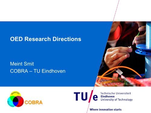
<strong>OED</strong> <strong>Research</strong> <strong>Directions</strong><br />
Meint Smit<br />
COBRA – TU Eindhoven
Outline<br />
• ECOC presentation about Generic Integration<br />
Technology<br />
• Short overview of running and new projects.<br />
Photonic Integration : Learning from CMOS ECOC’09, Wien 2/19
InP-based Photonic Integration:<br />
Learning from CMOS<br />
Meint Smit COBRA – TU Eindhoven<br />
Roel Baets IMEC – U Gent<br />
Mike Wale Oclaro
Transponder-based DWDM<br />
Receive Transmit<br />
FOE 2009, LS InP PIC in Dig Comm Networks, Nagarajan, Infinera, 169 Java Dr., Sunnyvale, CA 94089 | 4
Transmit<br />
Receive<br />
Infinera’s Photonic Integrated Circuit innovation<br />
100Gb/s Receive<br />
5mm<br />
100Gb/s Transmit<br />
Size, weight, power ↓ Reliability ↑<br />
FOE 2009, LS InP PIC in Dig Comm Networks, Nagarajan, Infinera, 169 Java Dr., Sunnyvale, CA 94089 | 5
Moore’s law for Photonic ICs<br />
Component count<br />
1000<br />
100<br />
10<br />
1<br />
1980 1990 2000 2010<br />
Photonic Integration : Learning from CMOS ECOC’09, Wien<br />
6/19<br />
Commercial<br />
COBRA/35P<br />
Philips/COBRA<br />
Alcatel/Opto+<br />
Lucent/Bell Labs<br />
NTT<br />
Infinera<br />
UCSB
What went wrong?<br />
• Since 1990 worldwide > 1 B$ invested in development of<br />
integration technologies<br />
• Almost all research was application driven<br />
• Therefore almost as many technologies as applications<br />
• For most of them: market too small for payback of<br />
investments<br />
• (By far too) many degrees of freedom<br />
• many different materials and technologies<br />
• many different component types<br />
• many different wavelength ranges and applications<br />
Photonic Integration : Learning from CMOS ECOC’09, Wien<br />
7/19
The (only?) way out<br />
• Develop a limited number of generic wafer-scale<br />
integration technologies, that can support a broad<br />
range of functionalities and applications<br />
• Move to a generic foundry model (as in CMOS)<br />
• Convergence of technologies<br />
• Decouple design (IP) from technology (IP)<br />
• Set up libraries and tools for ASPIC design<br />
• Organize training and design support for fabless<br />
companies<br />
• Work on market development<br />
(new applications)<br />
Photonic Integration : Learning from CMOS ECOC’09, Wien<br />
8/19
Generic Integration philosophy<br />
Electronic integration<br />
3 basic elements<br />
Photonic integration<br />
3 basic elements<br />
PWD<br />
PHM<br />
SOA<br />
Photonic Integration : Learning from CMOS ECOC’09, Wien<br />
ϕ<br />
Α<br />
9/19<br />
Waveguide<br />
Phase control<br />
Amplitude control<br />
SOA<br />
PWD<br />
PHM
Photonic Integration<br />
with 3 basic building blocks<br />
Passive<br />
Waveguide Devices<br />
waveguide<br />
curve<br />
MMI-coupler<br />
AWG-demux<br />
Photonic Integration : Learning from CMOS ECOC’09, Wien<br />
Devices with<br />
Phase Modulators<br />
phase modulator<br />
amplitude modulator<br />
2x2 switch<br />
WDM OXC<br />
10/19<br />
Devices with<br />
SOA<br />
Optical Amplifiers<br />
optical amplifier<br />
λ converter, ultrafast switch<br />
picosecond pulse laser<br />
multiwavelength laser
Examples<br />
optical crossconnect<br />
optical crossconnect<br />
WDM-TTD switch<br />
Cascaded WDM laser<br />
tunable multiwavelength laser<br />
multiwavelength laser<br />
wavelength converter picosecond pulse laser<br />
WDM ring laser<br />
Photonic Integration : Learning from CMOS ECOC’09, Wien<br />
11/19
Integrated Filtered Feedback – Tunable Laser<br />
Boudewijn Docter<br />
Wednesday 16:00, Hall E2<br />
Power in fiber [dBm]<br />
-25<br />
-35<br />
-45<br />
-55<br />
-65<br />
Gate 1<br />
Gate 2<br />
Gate 3<br />
Gate 4<br />
404 GHz<br />
1570 1575 1580 1585 1590 1595 1600<br />
Wavelength [nm]<br />
Photonic Integration : Learning from CMOS ECOC’09, Wien<br />
R<br />
ITU<br />
SOA<br />
Fabry-Perot Laser<br />
12/19<br />
R<br />
Feedback Filter<br />
SOA R<br />
Switching time: few ns<br />
Switching current ~ 10 mA
A Generic Integration Platform<br />
JePPIX:<br />
Joint European Platform for InP-based Photonic<br />
Integration of Components and Circuits<br />
Industrial partners: Oclaro, CIP, Philips,<br />
Alcatel-Thales III-V Lab,<br />
FhG-HHI, ASML, Aixtron, OPT<br />
Photonic CAD: Phoenix, Photon Design,<br />
Filarete<br />
Universities: COBRA –TU/e, Cambridge,<br />
Coordination: COBRA<br />
Step 1: Small-scale access to the COBRA process<br />
for research purposes (proof-of-concept)<br />
Step 2: Move to an industrial foundry (EuroPIC)<br />
Photonic Integration : Learning from CMOS ECOC’09, Wien<br />
13/19<br />
JePPIX
non-telecom applications<br />
Skin analysis equipment<br />
Readout units for fibre strain sensors<br />
Optical Coherence Tomography<br />
Skin Analysis<br />
Photonic Integration : Learning from CMOS ECOC’09, Wien<br />
14/19<br />
market<br />
Custom<br />
Technology<br />
2000 2010 2020<br />
Compact Frequency-comb<br />
generators for metrology<br />
Generic<br />
Technology
Component count<br />
Complexity of InP Photonic ICs?<br />
1000000<br />
100000<br />
10000<br />
1000<br />
100<br />
10<br />
1<br />
Nanophotonic<br />
Integration<br />
Technology<br />
1980 1990 2000 2010 2020 2030<br />
Photonic Integration : Learning from CMOS ECOC’09, Wien<br />
15/19<br />
Generic<br />
Integration<br />
Technology<br />
Digital<br />
Analog<br />
COBRA/35P<br />
Philips<br />
Opto+<br />
Lucent<br />
NTT<br />
Infinera<br />
UCSB
From analog to digital<br />
Martin Hill et al.,<br />
Nature, Vol. 432, 11 Nov. 2004, pp.206-209<br />
Photonic Integration : Learning from CMOS ECOC’09, Wien<br />
16/19<br />
Digital photonic flip-flop<br />
based on<br />
coupled micro-lasers<br />
Dimensions < 20 x 40 µm 2<br />
Switching time < 15 ps<br />
Switching energy < 6 fJ
IMOS: InP Membrane On Silicon<br />
Legend<br />
silicon<br />
silicon<br />
(a)<br />
(c)<br />
silicon<br />
IMOS (d)<br />
silicon<br />
(b)<br />
silicon<br />
silicon dioxide / BCB<br />
active InGaAsP/InP<br />
passive InP<br />
Photonic Integration : Learning from CMOS ECOC’09, Wien<br />
17/19<br />
Photonic Crystal Laser<br />
metal contacts<br />
active<br />
region<br />
Frederic Bordas<br />
Tuesday 16:30, Hall E2
Metallic and Plasmonic lasers<br />
A BREAKTHROUGH<br />
The world’s smallest electrically injected laser (diameter 250 nm)<br />
small active volume means low power and high speed<br />
Martin Hill et al., Nature Photonics, October 2007<br />
Gold<br />
InP<br />
Photonic Integration : Learning from CMOS ECOC’09, Wien<br />
18/19<br />
I th = 6 µA @ 77K
Latest Results for Plasmonic Lasers<br />
Room-temperature<br />
operation (pulsed)<br />
for 300 nm ridge<br />
width<br />
Plasmon laser<br />
operation for 80<br />
nm ridge width<br />
Photonic Integration : Learning from CMOS ECOC’09, Wien<br />
d ~80nm to<br />
340nm<br />
h=300nm<br />
19/19<br />
counts<br />
4.5<br />
4<br />
3.5<br />
3<br />
2.5<br />
2<br />
1.5<br />
1<br />
0.5<br />
x 104<br />
5<br />
Run 6, Row 1 dev #14, 298K<br />
3.7 V<br />
4.3 V<br />
5.8 V<br />
0<br />
1350 1400 1450 1500 1550 1600 1650<br />
wavelength (nm)
Potential<br />
100 nm<br />
silver<br />
InP<br />
• Integration of more than 100,000 lasers on a chip<br />
• Operating at speeds well beyond 1 THz<br />
Superior to high-speed transistors<br />
for ultrafast signal processing<br />
Photonic Integration : Learning from CMOS ECOC’09, Wien<br />
20/19
Component count<br />
Complexity of InP Photonic ICs?<br />
1000000<br />
100000<br />
10000<br />
1000<br />
100<br />
10<br />
1<br />
Nanophotonic<br />
Integration<br />
Technology<br />
1980 1990 2000 2010 2020 2030<br />
Photonic Integration : Learning from CMOS ECOC’09, Wien<br />
21/19<br />
IMOS<br />
Generic<br />
Integration<br />
Technology<br />
Digital<br />
Analog<br />
COBRA/35P<br />
Philips<br />
Opto+<br />
Lucent<br />
NTT<br />
Infinera<br />
UCSB
Acknowledgement: the COBRA – <strong>OED</strong> team<br />
EU-IST, NRC Photonics, IOP, STW
Generic Integration Technology<br />
Running projects<br />
• STW TWICE Chaotic encryption Jose Pozo Dec ‘10<br />
• STW EFFECT FF tunable lasers Boudewijn Docter, Jose Dec ‘10<br />
• MEMPHIS Plasmonic laser Milan Marell Dec ‘10<br />
MW-laser ASTRON Jing Zhao 2011<br />
• IOP PD OCT Bauke Tilma 2010<br />
• IOP PD FC-laser Saeed Tahvili 2011<br />
• EuroPIC MW-laser Flexpon Kate Lawnicuk 2012<br />
KM3 detector Stanislas Stopinski 2012<br />
Brillouin Sensor Manuela Felicetti 2012<br />
• KWR Baas Brillouin Sensor Klein Breteler Dec ‘10<br />
Sasbrink Dec ‘10<br />
• KWR ASML Scanner Adaptions Laurene Flannery Dec ‘10<br />
• KWR Philips Long λ platform 3 persons Dec ‘10<br />
Photonic Integration : Learning from CMOS ECOC’09, Wien 25/19
Generic Integration Technology<br />
New projects<br />
• JePPIX IP Passive component library 1 PhD<br />
Laser library (FP, DBR, Pulse) 1 PhD<br />
Pol handling + new modulation formats 1 PhD<br />
On-wafer test methodology 1 PhD<br />
Long wavelength QD’s 1 PD<br />
• JePPIX SA Coordinator + support for chip design & char<br />
• STW Perspectief Generic Photonic Integration Technologies 4 M€<br />
• IOP PD 2 Generic Fabrication Technology + Med. Appl. 10 M€<br />
• NWO Groot ASML wafer scanner<br />
• ePIXnet CA UPV / small role for TUE<br />
• IST STREP QD lasers / Univ Madrid<br />
• IST STREP 100 Gb ethernet TRX / UPV<br />
Photonic Integration : Learning from CMOS ECOC’09, Wien 26/19
Nanophotonic Integration Technology<br />
Running projects<br />
• Nanoned/NRC Pillar PhX Dima Dzibrou Mar ‘10<br />
• HISTORIC IMOS PhX laser Ray Zhang 2012<br />
• Phot for Comp IMOS Josselin Pello 2013<br />
New projects<br />
• FES NNI Plasmonic lasers 1 PhD<br />
• FET open Plasmonic lasers 1 PhD <strong>OED</strong>, 1 PhD PMP<br />
• IST Call 5 IMOS Active Cable WDM TX + RX TUE<br />
Polarisation MUX TUE<br />
Modulator Ugent<br />
Photonic Integration : Learning from CMOS ECOC’09, Wien 27/19
Nanophotonic Integration Technology<br />
Running Projects<br />
• JePPIX IP Passive component library 1 PhD<br />
Laser library (FP, DBR, Pulse) 1 PhD<br />
Pol handling + new modulation formats 1 PhD<br />
On-wafer test methodology 1 PhD<br />
Long wavelength QD’s 1 PD<br />
• JePPIX SA Coordinator + support for chip design & char<br />
• STW Perspectief Generic Photonic Integration Technologies 4 M€<br />
• IOP PD 2 Generic Fabrication Technology + Med. Appl. 10 M<br />
Photonic Integration : Learning from CMOS ECOC’09, Wien 28/19