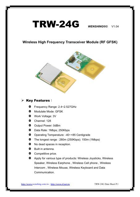
Wireless High Frequency Transceiver Module (RF GFSK)
Wireless High Frequency Transceiver Module (RF GFSK)
Wireless High Frequency Transceiver Module (RF GFSK)

You also want an ePaper? Increase the reach of your titles
YUMPU automatically turns print PDFs into web optimized ePapers that Google loves.
TRW-24G WENSHING®© V1.04<br />
<strong>Wireless</strong> <strong>High</strong> <strong>Frequency</strong> <strong>Transceiver</strong> <strong>Module</strong> (<strong>RF</strong> <strong>GFSK</strong>)<br />
Key Features:<br />
<strong>Frequency</strong> Range: 2.4~2.527GHz<br />
Modulate Mode: <strong>GFSK</strong><br />
Work Voltage: 3V<br />
Channel: 128<br />
Output Power: 0dBm<br />
Data Rate: 1Mbps; 250Kbps<br />
Operating Temperature: -40~+85 Centigrade<br />
The longest range : 280m (250Kbps); 150m (1Mbps)<br />
No dead spaces in reception.<br />
Built in antenna.<br />
Competitive price.<br />
Apply for various type of products: <strong>Wireless</strong> Joysticks, <strong>Wireless</strong><br />
Speaker, <strong>Wireless</strong> Earphone , <strong>Wireless</strong> Cell phone , <strong>Wireless</strong><br />
Intercom , <strong>Wireless</strong> Mouse, <strong>Wireless</strong> Keyboard and Data<br />
Communication.<br />
http://www.wenshing.com.tw ; http://www.rf.net.tw TRW-24G Data Sheet P.1
Graph:<br />
http://www.wenshing.com.tw ; http://www.rf.net.tw TRW-24G Data Sheet P.2
Specification :<br />
Conditions: VDD=+3V,VSS=0V,TA=-40 centigrade to +85 centigrade<br />
Symbol Parameter(condition) Min Typ Max Unit<br />
VDD Supply voltage 1.9 3.0 3.6 V<br />
TEMP Operating temperature -40 +27 +85 Centigrade<br />
fop Operating frequency 2400 2527 MHz<br />
R<strong>GFSK</strong> Data rate direct mode 250 1000 Kbps<br />
FCHANNEL Channel spacing 1 MHz<br />
IVDD<br />
IVDD<br />
IVDD<br />
IVDD<br />
RXSENS<br />
RXSENS<br />
Supply current one<br />
channel 250Kbps<br />
Supply current<br />
one channel 1000Kbps<br />
Supply current<br />
two channels 250Kbps<br />
Supply current<br />
two channels 1000Kbps<br />
Sensitivity<br />
at 0.1%BER(@250Kbps)<br />
Sensitivity<br />
at 0.1%BER(@1000Kbps)<br />
18 mA<br />
19 mA<br />
23 mA<br />
25 mA<br />
-90 dBm<br />
-80 dBm<br />
http://www.wenshing.com.tw ; http://www.rf.net.tw TRW-24G Data Sheet P.3
Demo Circuit Diagram :<br />
http://www.wenshing.com.tw ; http://www.rf.net.tw TRW-24G Data Sheet P.4
http://www.wenshing.com.tw ; http://www.rf.net.tw TRW-24G Data Sheet P.5
Circuit Description:<br />
ShockBurst TM<br />
The ShockBurst TM technology uses on-chip FIFO to clock in data at a low data<br />
rate and transmit at a very high rate thus enabling extremely power reduction.<br />
When operation the TRW-24G in ShockBurst TM ,you gain access to the high<br />
data rates(1 Mbps)offered by the 2.4GHz band without the need of a costly,<br />
high-speed micro controller (MCU) for data processing.<br />
By putting all high speed signal processing related to <strong>RF</strong> protocol on-chip, the<br />
TRW-24G offers the following benefits:<br />
<strong>High</strong>ly reduced current consumption.<br />
Lower system cost (facilitates use of less expensive micro controller).<br />
Greatly reduced risk of ‘on-air’ collisions due to short transmission time.<br />
The TRW-24G can be programmed using a simple 3-wire interface where the<br />
data rate is decided by the speed of the micro controller.<br />
By allowing the digital part of the application to run at low speed while<br />
maximizing the data rate on the <strong>RF</strong> link, the n<strong>RF</strong> ShockBurst TM mode reduces<br />
the average current consumption in applications considerably.<br />
http://www.wenshing.com.tw ; http://www.rf.net.tw TRW-24G Data Sheet P.6
ShockBurst TM principle:<br />
When the TRW-24G is configured in ShockBurst TM , TX or RX operation is<br />
conducted in the following way (10 kbps for the example only).<br />
Figure 4 Clocking in data with MCU and sending with ShockBurst TM<br />
technology<br />
Time mS<br />
Figure1 Current consumption with & without ShockBurst TM technology<br />
http://www.wenshing.com.tw ; http://www.rf.net.tw TRW-24G Data Sheet P.7
Figure 2 Flow Chart shockBurst TM Transmit of TRW-24G<br />
n<strong>RF</strong>2401 ShockBurst TM Transmit:<br />
MCU interface pins:CE,CLK1,DATA<br />
1. When the application MCU has data to send, set CE high. This<br />
activates TRW-24G on-board data processing.<br />
2. The address of the receiving node(RX address) and payload data<br />
is clocked into the TRW-24G. The application protocol or MCU<br />
sets the speed .<br />
3. MCU sets CE low, this activates a TRW-24G ShockBurst TM<br />
transmission.<br />
4. TRW-24G ShockBurst TM :<br />
http://www.wenshing.com.tw ; http://www.rf.net.tw TRW-24G Data Sheet P.8
<strong>RF</strong> front end is powered up.<br />
<strong>RF</strong> package is completed (preamble added, CRC calculated).<br />
Data is transmitted at high speed (250kbps or 1 Mbps<br />
configured by user).<br />
TRW-24G return to stand-by when finished.<br />
Figure 3 Flow Chart ShockBurst TM Receive of TRW-24G.<br />
http://www.wenshing.com.tw ; http://www.rf.net.tw TRW-24G Data Sheet P.9
TRW-24G ShockBurst TM Receive:<br />
MCU interface pins: CE, DR1, CLK1 and DATA (one RX channel<br />
receive)<br />
1. Correct address and size of payload of incoming <strong>RF</strong><br />
packages are set when TRW-24G is configured to<br />
ShockBurst TM RX.<br />
2. To activate RX , set CE high.<br />
3. After 200us settling, TRW-24G is monitoring the air for<br />
incoming communication.<br />
4. When a valid package has been received (correct<br />
address and CRC found), TRW-24G removes the<br />
preamble, address and CRC bits.<br />
5. TRW-24G then notifies (interrupts) the MCU by setting<br />
the DR1 pin high.<br />
6. MCU may (or may not) set the CE low to disable the <strong>RF</strong><br />
front end (low current mode).<br />
7. The MCU will clock out just the payload data at a suitable<br />
rate (ex,10 kbps).<br />
8. When all payload data is retrieved TRW-24G sets DR1<br />
low again, and is ready for new incoming data package if<br />
CE is kept high during data download. If the CE was set<br />
low, a new start up sequence can begin, see Figure 12.<br />
Duoceiver TM Simultaneous Two Channel Receive Mode:<br />
In both ShockBurst TM modes the TRW-24G can facilitate simultaneous<br />
reception of two parallel independent frequency channels at the maximum<br />
data rate.<br />
This means:<br />
TRW-24G can receive data from two 1Mbps transmitters (ex:<br />
TRW-24G or TRW-24G) 8MHz (8 frequency channels) apart<br />
through one antenna interface.<br />
The output from the two data channels is fed to two separate<br />
MCU interfaces.<br />
Data channel 1:CLK1,DATA,and DR1<br />
Data channel 2:CLK2,DOUT2,and DR2<br />
DR1 and DR2 are available only in ShockBurst TM .<br />
The TRW-24G DuoCeiver TM technology provides 2 separate dedicated data<br />
channels for RX and replaces the need for two, stand alone receiver systems.<br />
http://www.wenshing.com.tw ; http://www.rf.net.tw TRW-24G Data Sheet P.10
Figure 4 Simultaneous 2 channel receive on TRW-24G<br />
There is one absolute requirement for using the second data channel. For the<br />
TRW-24G to be able to receive at the second data channel the frequency<br />
channel must be 8MHz higher than the frequency of data channel 1. The<br />
TRW-24G must be programmed to receive at the frequency of data channel 1.<br />
No time multiplexing is used in TRW-24G to fulfil this function. In direct mode<br />
the MCU must be able to handle two simultaneously incoming data packets if it<br />
is not multiplexing between the two data channels. In ShockBurst TM it is<br />
possible for the MCU to clock out one data channel at a time while data on the<br />
other data channel waits for MCU availability, without any lost data packets,<br />
and by doing so reduce the needed performance of the MCU.<br />
Figure 5 DuoCeiver TM with two simultaneously independent receive<br />
channels<br />
Device Configuration:<br />
All configuration of theTRW-24G is done via 3-wire interface to a single<br />
configuration register. The configuration word can be up to 15 bytes long for<br />
ShockBurst TM .<br />
http://www.wenshing.com.tw ; http://www.rf.net.tw TRW-24G Data Sheet P.11
Configuration or ShockBurst TM operation:<br />
The configuration word in ShockBurst TM enables theTRW-24G to handle the<br />
<strong>RF</strong> protocol. Once the protocol is completed and loaded intoTRW-24G only<br />
one byte, bit [7:0], needs to be updated during actual operation.<br />
The configuration blocks dedicated to ShockBurst TM is as follows:<br />
Payload section width: Specifies the number of payload bits in a <strong>RF</strong><br />
package. This enables theTRW-24G to distinguish between payload data<br />
and the CRC bytes in a received package.<br />
Address width: Sets the number of bits used for address in the <strong>RF</strong> package,<br />
This enables theTRW-24G to distinguish between address and payload<br />
data.<br />
Address (RX Channel 1 and 2): Destination address for received data.<br />
CRC: Enables TRW-24G on-chip CRC generation and de-coding.<br />
NOTE:<br />
These configuration blocks, with the exception of the CRC, are dedicated for<br />
the packages that a TRW-24G is to receive.<br />
In TX mode, the MCU must generate an address and a payload section that<br />
fits the configuration of theTRW-24G that is to receive the data.<br />
When using theTRW-24G on-chip CRC feature ensure that CRC is enabled<br />
and uses the same length for both the TX and RX devices.<br />
Figure 10 Data packet set-up<br />
http://www.wenshing.com.tw ; http://www.rf.net.tw TRW-24G Data Sheet P.12
Configuration word overview:<br />
Table 1 Table of configuration words<br />
The configuration word is shifted in MSB first on positive CLK1 edges, New<br />
configuration is enabled on the falling edge of CS.<br />
NOTE:<br />
On the falling edge of CS, theTRW-24G updates the number of bits actually<br />
shifted in during the last configuration.<br />
Ex:<br />
If theTRW-24G is to be configured for 2 channel RX in ShockBurst TM , a total of<br />
120 bits must be shifted in during the first configuration after VDD is applied.<br />
Once the wanted protocol, modus and <strong>RF</strong> channel are set, only one bit (RXEN)<br />
is shifted in to switch between RX and TX.<br />
http://www.wenshing.com.tw ; http://www.rf.net.tw TRW-24G Data Sheet P.13
Configuration Word Detailed Description:<br />
The following describes the function of the 144 bits (bit 143=MSB) that is used<br />
to configure the TRW-24G<br />
General Device Configuration: bit [15:0]<br />
ShockBurst TM Configuration: bit [119:0]<br />
Test Configuration: bit [143:120]<br />
Table 2 Configuration data word<br />
http://www.wenshing.com.tw ; http://www.rf.net.tw TRW-24G Data Sheet P.14
The MSB bit should be loaded first into the configuration register.<br />
Default configuration word:<br />
h8E08.1C20.2000.0000.00E7.0000.0000.E721.0F04.<br />
ShockBurst TM configuration:<br />
The section B[119:16] contains the segments of the configuration register<br />
dedicated to ShockBurst TM operational protocol. After VDD is turned on<br />
ShockBurst TM configuration is done once and remains set whilst VDD is<br />
present, During operation only the first byte for frequency channel and RX/TX<br />
switching need to be changed.<br />
PLL_CTRL<br />
Table 10 PLL setting<br />
Bit 121-120:<br />
PLL_CTRL: Controls the setting of the PLL for test purposes. With closed PLL<br />
in TX no deviation will be present.<br />
DATAx_W<br />
Table 4 Number of bits in payload<br />
Bit 119-112:<br />
DATA2_W: Length of <strong>RF</strong> package payload section for receive-channel 2.<br />
Bit 111-104:<br />
DATA1_W: Length of <strong>RF</strong> package payload section for receive-channel 1.<br />
NOTE:<br />
The total number of bits in a ShockBurst TM <strong>RF</strong> package may not exceed 256!<br />
Maximum length of payload section is hence given by:<br />
DATAx_W(bits)=256-ADDR_W-CRC<br />
http://www.wenshing.com.tw ; http://www.rf.net.tw TRW-24G Data Sheet P.15
Where:<br />
ADDR_W: length of RX address set in configuration word B [23:18]<br />
CRC: check sum, 8 or 16 bits set in configuration word B [17]<br />
PRE: preamble, 4 or 8 bits are automatically included<br />
Shorter address and CRC leaves more room for payload data in each<br />
package.<br />
ADDRx<br />
Table 5 Address of receiver #2 and receiver #1<br />
Bit 103-64:<br />
ADDR2: Receiver address channel 2, up to 40 bit.<br />
Bit 63-24:<br />
ADDR1: Receiver address channel 1, up to 40 bit.<br />
NOTE:<br />
Bits in ADDRx exceeding the address width set in ADDR_W are redundant<br />
and can be set to logic 0.<br />
ADDR_W & CRC<br />
Table 6 Number of bits reserved for RX address + CRC setting<br />
Bit 23-18:<br />
ADDR_W: Number of bits reserved for RX address in ShockBurst TM packages.<br />
NOTE:<br />
Maximum number of address bits is 40 (5 bytes). Values over 40 in ADDR_W<br />
are not valid.<br />
Bit 17:<br />
CRC_L: CRC length to be calculated by TRW-24G in<br />
ShockBurst TM .<br />
Logic 0: 8 bit CRC<br />
Logic 1: 16 bit CRC<br />
Bit 16:<br />
CRC_EN: Enables on-chip CRC generation (TX) and verification<br />
(RX).<br />
Logic 0: On-chip CRC generation/checking disabled<br />
Logic 1: On-chip CRC generation/checking enabled<br />
http://www.wenshing.com.tw ; http://www.rf.net.tw TRW-24G Data Sheet P.16
NOTE:<br />
An 8 bit CRC will increase the number of payload bits possible in each<br />
ShockBurst TM data packet, but will also reduce the system integrigy.<br />
General device configuration:<br />
This section of the configuration word handles <strong>RF</strong> and device related<br />
parameters.<br />
Modes:<br />
Bit 15:<br />
RX2_EN:<br />
Logic 0: One channel receive<br />
Logic 1: Two channels receive<br />
Table 7 <strong>RF</strong> operational settings<br />
NOTE:<br />
In two channels receive, the TRW-24G receives on two, separate frequency<br />
channels simultaneously. The frequency of receive channel 1 is set in the<br />
configuration word B[7-1], receive channel 2 is always 8 channels (8 MHz)<br />
above receive channel 1.<br />
Bit 14:<br />
Communication Mode:<br />
Logic 1: n<strong>RF</strong>2401 operates in ShockBurst TM mode<br />
Bit 13:<br />
<strong>RF</strong> Data Rate:<br />
Logic 0: 250 kbps<br />
Logic 1: 1 Mbps<br />
NOTE:<br />
Utilizing 250 kbps instead of 1 Mbps will improve the receiver sensitivity by 10<br />
dB. 1 Mbps requires 16MHz crystal.<br />
Bit 12-10:<br />
D12 D11 D10<br />
0 1 1<br />
Table 8<br />
http://www.wenshing.com.tw ; http://www.rf.net.tw TRW-24G Data Sheet P.17
Bit 9-8:<br />
<strong>RF</strong>_PWR: Sets TRW-24G <strong>RF</strong> output power in transmit mode:<br />
<strong>RF</strong> channel & direction:<br />
Table 9 <strong>RF</strong> output power setting<br />
Table 10 <strong>Frequency</strong> channel + RX/TX setting<br />
Bit 7-1:<br />
<strong>RF</strong>_CH#: Sets the frequency channel the n<strong>RF</strong>2401 operates on.<br />
The channel frequency in transmit is given by:<br />
Channel<strong>RF</strong> = 2400 MHz + <strong>RF</strong>_CH# ・1.0 MHz<br />
<strong>RF</strong>_CH # : between 2400MHz and 2527MHz may be set.<br />
The channel frequency in data channel 1 is given by:<br />
Channel<strong>RF</strong> = 2400 MHz + <strong>RF</strong>_CH#・1.0 MHz (Receive at PIN#8)<br />
<strong>RF</strong>_CH # : between 2400MHz and 2524MHz may be set.<br />
NOTE:<br />
The channels above 83 can only be utilized in certain territories (ex: Japan)<br />
The channel frequency in data channel 2 is given by:<br />
Channel<strong>RF</strong> = 2400 MHz + <strong>RF</strong>_CH#・1.0 MHz + 8MHz (Receive at PIN#4)<br />
<strong>RF</strong>_CH # : between 2408MHz and 2524MHz may be set.<br />
Bit 0:<br />
Set active mode:<br />
Logic 0: transmit mode<br />
Logic 1: receive mode<br />
http://www.wenshing.com.tw ; http://www.rf.net.tw TRW-24G Data Sheet P.18
The data packet for both ShockBurst TM mode and direct mode communication<br />
is divided into 4 sections. These are:<br />
1. PREAMBLE · The preamble field is required in ShockBurst.<br />
· The address field is required in ShockBurst. mode.<br />
2. ADDRESS · 8 to 40 bits length.<br />
· Address automatically removed from received packet in<br />
ShockBurst.mode<br />
· The data to be transmitted<br />
3. PAYLOAD · In Shock-Burst mode payload size is 256 bits minus the<br />
Following :(Address: 8 to 40 bits. + CRC 8 or 16 bits).<br />
4. CRC<br />
Data Package Description:<br />
· 8 or 16 bits length<br />
· The CRC is stripped from the received output data.<br />
Figure 7 Data Package Diagram<br />
http://www.wenshing.com.tw ; http://www.rf.net.tw TRW-24G Data Sheet P.19
TRW-24G configuration data is from a high level start.<br />
Example: In ShockBurth launching mode, it is to a passage in the<br />
2410MHz to 1Mbps Rate transmission<br />
Bit143 Bit142 Bit141 Bit140 Bit139 Bit138 Bit137 Bit136<br />
1 0 0 0 1 1 1 0<br />
Bit135 Bit134 Bit133 Bit132 Bit131 Bit130 Bit129 Bit128<br />
0 0 0 0 1 0 0 0<br />
Bit127 Bit126 Bit125 Bit124 Bit123 Bit122 Bit121 Bit120<br />
0 0 0 1 1 1 0 0<br />
Bit119 Bit118 Bit117 Bit116 Bit115 Bit114 Bit113 Bit112<br />
1 1 0 0 1 0 0 0<br />
Bit111 Bit110 Bit109 Bit108 Bit107 Bit106 Bit105 Bit104<br />
1 1 0 0 1 0 0 0<br />
Bit103 Bit102 Bit101 Bit100 Bit99 Bit98 Bit97 Bit96<br />
1 1 0 0 0 0 0 0<br />
Bit95 Bit94 Bit93 Bit92 Bit91 Bit90 Bit89 Bit88<br />
1 0 1 0 1 0 1 0<br />
Bit87 Bit86 Bit85 Bit84 Bit83 Bit82 Bit81 Bit80<br />
0 1 0 1 0 1 0 1<br />
Bit79 Bit78 Bit77 Bit76 Bit75 Bit74 Bit73 Bit72<br />
1 0 1 0 1 0 1 0<br />
Bit71 Bit70 Bit69 Bit68 Bit67 Bit66 Bit65 Bit64<br />
0 1 0 1 0 1 0 1<br />
Bit63 Bit62 Bit61 Bit60 Bit59 Bit58 Bit57 Bit56<br />
1 0 1 0 1 0 1 0<br />
Bit55 Bit54 Bit53 Bit52 Bit51 Bit50 Bit49 Bit48<br />
0 1 0 1 0 1 0 1<br />
Bit47 Bit46 Bit45 Bit44 Bit43 Bit42 Bit41 Bit40<br />
1 0 1 0 1 0 1 0<br />
Bit39 Bit38 Bit37 Bit36 Bit35 Bit34 Bit33 Bit32<br />
0 1 0 1 0 1 0 1<br />
Bit31 Bit30 Bit29 Bit28 Bit27 Bit26 Bit25 Bit24<br />
1 0 1 0 1 0 1 0<br />
Bit23 Bit22 Bit21 Bit20 Bit19 Bit18 Bit17 Bit16<br />
1 0 1 0 0 0 1 1<br />
Bit15 Bit14 Bit13 Bit12 Bit11 Bit10 Bit9 Bit8<br />
0 1 1 0 1 1 1 1<br />
Bit7 Bit6 Bit5 Bit4 Bit3 Bit2 Bit1 Bit0<br />
0 0 0 1 0 1 0 0<br />
http://www.wenshing.com.tw ; http://www.rf.net.tw TRW-24G Data Sheet P.20
Example: ShockBurth in the receive mode, it is to a passage in the<br />
2410MHz to 1Mbps Rate reception.<br />
Bit143 Bit142 Bit141 Bit140 Bit139 Bit138 Bit137 Bit136<br />
1 0 0 0 1 1 1 0<br />
Bit135 Bit134 Bit133 Bit132 Bit131 Bit130 Bit129 Bit128<br />
0 0 0 0 1 0 0 0<br />
Bit127 Bit126 Bit125 Bit124 Bit123 Bit122 Bit121 Bit120<br />
0 0 0 1 1 1 0 0<br />
Bit119 Bit118 Bit117 Bit116 Bit115 Bit114 Bit113 Bit112<br />
1 1 0 0 1 0 0 0<br />
Bit111 Bit110 Bit109 Bit108 Bit107 Bit106 Bit105 Bit104<br />
1 1 0 0 1 0 0 0<br />
Bit103 Bit102 Bit101 Bit100 Bit99 Bit98 Bit97 Bit96<br />
1 1 0 0 0 0 0 0<br />
Bit95 Bit94 Bit93 Bit92 Bit91 Bit90 Bit89 Bit88<br />
1 0 1 0 1 0 1 0<br />
Bit87 Bit86 Bit85 Bit84 Bit83 Bit82 Bit81 Bit80<br />
0 1 0 1 0 1 0 1<br />
Bit79 Bit78 Bit77 Bit76 Bit75 Bit74 Bit73 Bit72<br />
1 0 1 0 1 0 1 0<br />
Bit71 Bit70 Bit69 Bit68 Bit67 Bit66 Bit65 Bit64<br />
0 1 0 1 0 1 0 1<br />
Bit63 Bit62 Bit61 Bit60 Bit59 Bit58 Bit57 Bit56<br />
1 0 1 0 1 0 1 0<br />
Bit55 Bit54 Bit53 Bit52 Bit51 Bit50 Bit49 Bit48<br />
0 1 0 1 0 1 0 1<br />
Bit47 Bit46 Bit45 Bit44 Bit43 Bit42 Bit41 Bit40<br />
1 0 1 0 1 0 1 0<br />
Bit39 Bit38 Bit37 Bit36 Bit35 Bit34 Bit33 Bit32<br />
0 1 0 1 0 1 0 1<br />
Bit31 Bit30 Bit29 Bit28 Bit27 Bit26 Bit25 Bit24<br />
1 0 1 0 1 0 1 0<br />
Bit23 Bit22 Bit21 Bit20 Bit19 Bit18 Bit17 Bit16<br />
1 0 1 0 0 0 1 1<br />
Bit15 Bit14 Bit13 Bit12 Bit11 Bit10 Bit9 Bit8<br />
0 1 1 0 1 1 1 1<br />
Bit7 Bit6 Bit5 Bit4 Bit3 Bit2 Bit1 Bit0<br />
0 0 0 1 0 1 0 1<br />
http://www.wenshing.com.tw ; http://www.rf.net.tw TRW-24G Data Sheet P.21
Example: in ShockBurth launching mode, it is to a passage in the<br />
2410MHz to 250Kbps Rate fired.<br />
Bit143 Bit142 Bit141 Bit140 Bit139 Bit138 Bit137 Bit136<br />
1 0 0 0 1 1 1 0<br />
Bit135 Bit134 Bit133 Bit132 Bit131 Bit130 Bit129 Bit128<br />
0 0 0 0 1 0 0 0<br />
Bit127 Bit126 Bit125 Bit124 Bit123 Bit122 Bit121 Bit120<br />
0 0 0 1 1 1 0 0<br />
Bit119 Bit118 Bit117 Bit116 Bit115 Bit114 Bit113 Bit112<br />
1 1 0 0 1 0 0 0<br />
Bit111 Bit110 Bit109 Bit108 Bit107 Bit106 Bit105 Bit104<br />
1 1 0 0 1 0 0 0<br />
Bit103 Bit102 Bit101 Bit100 Bit99 Bit98 Bit97 Bit96<br />
1 1 0 0 0 0 0 0<br />
Bit95 Bit94 Bit93 Bit92 Bit91 Bit90 Bit89 Bit88<br />
1 0 1 0 1 0 1 0<br />
Bit87 Bit86 Bit85 Bit84 Bit83 Bit82 Bit81 Bit80<br />
0 1 0 1 0 1 0 1<br />
Bit79 Bit78 Bit77 Bit76 Bit75 Bit74 Bit73 Bit72<br />
1 0 1 0 1 0 1 0<br />
Bit71 Bit70 Bit69 Bit68 Bit67 Bit66 Bit65 Bit64<br />
0 1 0 1 0 1 0 1<br />
Bit63 Bit62 Bit61 Bit60 Bit59 Bit58 Bit57 Bit56<br />
1 0 1 0 1 0 1 0<br />
Bit55 Bit54 Bit53 Bit52 Bit51 Bit50 Bit49 Bit48<br />
0 1 0 1 0 1 0 1<br />
Bit47 Bit46 Bit45 Bit44 Bit43 Bit42 Bit41 Bit40<br />
1 0 1 0 1 0 1 0<br />
Bit39 Bit38 Bit37 Bit36 Bit35 Bit34 Bit33 Bit32<br />
0 1 0 1 0 1 0 1<br />
Bit31 Bit30 Bit29 Bit28 Bit27 Bit26 Bit25 Bit24<br />
1 0 1 0 1 0 1 0<br />
Bit23 Bit22 Bit21 Bit20 Bit19 Bit18 Bit17 Bit16<br />
1 0 1 0 0 0 1 1<br />
Bit15 Bit14 Bit13 Bit12 Bit11 Bit10 Bit9 Bit8<br />
0 1 0 0 1 1 1 1<br />
Bit7 Bit6 Bit5 Bit4 Bit3 Bit2 Bit1 Bit0<br />
0 0 0 1 0 1 0 0<br />
http://www.wenshing.com.tw ; http://www.rf.net.tw TRW-24G Data Sheet P.22
Example: ShockBurth in the receive mode, it is to a passage in the<br />
2410MHz to 250Kbps Rate reception.<br />
Bit143 Bit142 Bit141 Bit140 Bit139 Bit138 Bit137 Bit136<br />
1 0 0 0 1 1 1 0<br />
Bit135 Bit134 Bit133 Bit132 Bit131 Bit130 Bit129 Bit128<br />
0 0 0 0 1 0 0 0<br />
Bit127 Bit126 Bit125 Bit124 Bit123 Bit122 Bit121 Bit120<br />
0 0 0 1 1 1 0 0<br />
Bit119 Bit118 Bit117 Bit116 Bit115 Bit114 Bit113 Bit112<br />
1 1 0 0 1 0 0 0<br />
Bit111 Bit110 Bit109 Bit108 Bit107 Bit106 Bit105 Bit104<br />
1 1 0 0 1 0 0 0<br />
Bit103 Bit102 Bit101 Bit100 Bit99 Bit98 Bit97 Bit96<br />
1 1 0 0 0 0 0 0<br />
Bit95 Bit94 Bit93 Bit92 Bit91 Bit90 Bit89 Bit88<br />
1 0 1 0 1 0 1 0<br />
Bit87 Bit86 Bit85 Bit84 Bit83 Bit82 Bit81 Bit80<br />
0 1 0 1 0 1 0 1<br />
Bit79 Bit78 Bit77 Bit76 Bit75 Bit74 Bit73 Bit72<br />
1 0 1 0 1 0 1 0<br />
Bit71 Bit70 Bit69 Bit68 Bit67 Bit66 Bit65 Bit64<br />
0 1 0 1 0 1 0 1<br />
Bit63 Bit62 Bit61 Bit60 Bit59 Bit58 Bit57 Bit56<br />
1 0 1 0 1 0 1 0<br />
Bit55 Bit54 Bit53 Bit52 Bit51 Bit50 Bit49 Bit48<br />
0 1 0 1 0 1 0 1<br />
Bit47 Bit46 Bit45 Bit44 Bit43 Bit42 Bit41 Bit40<br />
1 0 1 0 1 0 1 0<br />
Bit39 Bit38 Bit37 Bit36 Bit35 Bit34 Bit33 Bit32<br />
0 1 0 1 0 1 0 1<br />
Bit31 Bit30 Bit29 Bit28 Bit27 Bit26 Bit25 Bit24<br />
1 0 1 0 1 0 1 0<br />
Bit23 Bit22 Bit21 Bit20 Bit19 Bit18 Bit17 Bit16<br />
1 0 1 0 0 0 1 1<br />
Bit15 Bit14 Bit13 Bit12 Bit11 Bit10 Bit9 Bit8<br />
0 1 0 0 1 1 1 1<br />
Bit7 Bit6 Bit5 Bit4 Bit3 Bit2 Bit1 Bit0<br />
0 0 0 1 0 1 0 1<br />
http://www.wenshing.com.tw ; http://www.rf.net.tw TRW-24G Data Sheet P.23
Example: ShockBurth in the receive mode, it is with two channels in the<br />
2410MHz to 1Mbps Rate reception.<br />
Bit143 Bit142 Bit141 Bit140 Bit139 Bit138 Bit137 Bit136<br />
1 0 0 0 1 1 1 0<br />
Bit135 Bit134 Bit133 Bit132 Bit131 Bit130 Bit129 Bit128<br />
0 0 0 0 1 0 0 0<br />
Bit127 Bit126 Bit125 Bit124 Bit123 Bit122 Bit121 Bit120<br />
0 0 0 1 1 1 0 0<br />
Bit119 Bit118 Bit117 Bit116 Bit115 Bit114 Bit113 Bit112<br />
1 1 0 0 1 0 0 0<br />
Bit111 Bit110 Bit109 Bit108 Bit107 Bit106 Bit105 Bit104<br />
1 1 0 0 1 0 0 0<br />
Bit103 Bit102 Bit101 Bit100 Bit99 Bit98 Bit97 Bit96<br />
1 1 0 0 0 0 0 0<br />
Bit95 Bit94 Bit93 Bit92 Bit91 Bit90 Bit89 Bit88<br />
1 0 1 0 1 0 1 0<br />
Bit87 Bit86 Bit85 Bit84 Bit83 Bit82 Bit81 Bit80<br />
0 1 0 1 0 1 0 1<br />
Bit79 Bit78 Bit77 Bit76 Bit75 Bit74 Bit73 Bit72<br />
1 0 1 0 1 0 1 0<br />
Bit71 Bit70 Bit69 Bit68 Bit67 Bit66 Bit65 Bit64<br />
0 1 0 1 0 1 0 1<br />
Bit63 Bit62 Bit61 Bit60 Bit59 Bit58 Bit57 Bit56<br />
1 0 1 0 1 0 1 0<br />
Bit55 Bit54 Bit53 Bit52 Bit51 Bit50 Bit49 Bit48<br />
0 1 0 1 0 1 0 1<br />
Bit47 Bit46 Bit45 Bit44 Bit43 Bit42 Bit41 Bit40<br />
1 0 1 0 1 0 1 0<br />
Bit39 Bit38 Bit37 Bit36 Bit35 Bit34 Bit33 Bit32<br />
0 1 0 1 0 1 0 1<br />
Bit31 Bit30 Bit29 Bit28 Bit27 Bit26 Bit25 Bit24<br />
1 0 1 0 1 0 1 0<br />
Bit23 Bit22 Bit21 Bit20 Bit19 Bit18 Bit17 Bit16<br />
1 0 1 0 0 0 1 1<br />
Bit15 Bit14 Bit13 Bit12 Bit11 Bit10 Bit9 Bit8<br />
1 1 1 0 1 1 1 1<br />
Bit7 Bit6 Bit5 Bit4 Bit3 Bit2 Bit1 Bit0<br />
0 0 0 1 0 1 0 1<br />
http://www.wenshing.com.tw ; http://www.rf.net.tw TRW-24G Data Sheet P.24
Example: ShockBurth in the receive mode, it is with two channels in the<br />
2410MHz to 250Kbps Rate reception.<br />
Bit143 Bit142 Bit141 Bit140 Bit139 Bit138 Bit137 Bit136<br />
1 0 0 0 1 1 1 0<br />
Bit135 Bit134 Bit133 Bit132 Bit131 Bit130 Bit129 Bit128<br />
0 0 0 0 1 0 0 0<br />
Bit127 Bit126 Bit125 Bit124 Bit123 Bit122 Bit121 Bit120<br />
0 0 0 1 1 1 0 0<br />
Bit119 Bit118 Bit117 Bit116 Bit115 Bit114 Bit113 Bit112<br />
1 1 0 0 1 0 0 0<br />
Bit111 Bit110 Bit109 Bit108 Bit107 Bit106 Bit105 Bit104<br />
1 1 0 0 1 0 0 0<br />
Bit103 Bit102 Bit101 Bit100 Bit99 Bit98 Bit97 Bit96<br />
1 1 0 0 0 0 0 0<br />
Bit95 Bit94 Bit93 Bit92 Bit91 Bit90 Bit89 Bit88<br />
1 0 1 0 1 0 1 0<br />
Bit87 Bit86 Bit85 Bit84 Bit83 Bit82 Bit81 Bit80<br />
0 1 0 1 0 1 0 1<br />
Bit79 Bit78 Bit77 Bit76 Bit75 Bit74 Bit73 Bit72<br />
1 0 1 0 1 0 1 0<br />
Bit71 Bit70 Bit69 Bit68 Bit67 Bit66 Bit65 Bit64<br />
0 1 0 1 0 1 0 1<br />
Bit63 Bit62 Bit61 Bit60 Bit59 Bit58 Bit57 Bit56<br />
1 0 1 0 1 0 1 0<br />
Bit55 Bit54 Bit53 Bit52 Bit51 Bit50 Bit49 Bit48<br />
0 1 0 1 0 1 0 1<br />
Bit47 Bit46 Bit45 Bit44 Bit43 Bit42 Bit41 Bit40<br />
1 0 1 0 1 0 1 0<br />
Bit39 Bit38 Bit37 Bit36 Bit35 Bit34 Bit33 Bit32<br />
0 1 0 1 0 1 0 1<br />
Bit31 Bit30 Bit29 Bit28 Bit27 Bit26 Bit25 Bit24<br />
1 0 1 0 1 0 1 0<br />
Bit23 Bit22 Bit21 Bit20 Bit19 Bit18 Bit17 Bit16<br />
1 0 1 0 0 0 1 1<br />
Bit15 Bit14 Bit13 Bit12 Bit11 Bit10 Bit9 Bit8<br />
1 1 0 0 1 1 1 1<br />
Bit7 Bit6 Bit5 Bit4 Bit3 Bit2 Bit1 Bit0<br />
0 0 0 1 0 1 0 1<br />
http://www.wenshing.com.tw ; http://www.rf.net.tw TRW-24G Data Sheet P.25
TRW-24G configuration data is from a high level began.<br />
Example: In the direct launch mode, it is to a passage in the 2410MHz<br />
channel to 1Mbps Rate fired.<br />
Bit143 Bit142 Bit141 Bit140 Bit139 Bit138 Bit137 Bit136<br />
1 0 0 0 1 1 1 0<br />
Bit135 Bit134 Bit133 Bit132 Bit131 Bit130 Bit129 Bit128<br />
0 0 0 0 1 0 0 0<br />
Bit127 Bit126 Bit125 Bit124 Bit123 Bit122 Bit121 Bit120<br />
0 0 0 1 1 1 0 0<br />
Bit119 Bit118 Bit117 Bit116 Bit115 Bit114 Bit113 Bit112<br />
1 1 0 0 1 0 0 0<br />
Bit111 Bit110 Bit109 Bit108 Bit107 Bit106 Bit105 Bit104<br />
1 1 0 0 1 0 0 0<br />
Bit103 Bit102 Bit101 Bit100 Bit99 Bit98 Bit97 Bit96<br />
1 1 0 0 0 0 0 0<br />
Bit95 Bit94 Bit93 Bit92 Bit91 Bit90 Bit89 Bit88<br />
1 0 1 0 1 0 1 0<br />
Bit87 Bit86 Bit85 Bit84 Bit83 Bit82 Bit81 Bit80<br />
0 1 0 1 0 1 0 1<br />
Bit79 Bit78 Bit77 Bit76 Bit75 Bit74 Bit73 Bit72<br />
1 0 1 0 1 0 1 0<br />
Bit71 Bit70 Bit69 Bit68 Bit67 Bit66 Bit65 Bit64<br />
0 1 0 1 0 1 0 1<br />
Bit63 Bit62 Bit61 Bit60 Bit59 Bit58 Bit57 Bit56<br />
1 0 1 0 1 0 1 0<br />
Bit55 Bit54 Bit53 Bit52 Bit51 Bit50 Bit49 Bit48<br />
0 1 0 1 0 1 0 1<br />
Bit47 Bit46 Bit45 Bit44 Bit43 Bit42 Bit41 Bit40<br />
1 0 1 0 1 0 1 0<br />
Bit39 Bit38 Bit37 Bit36 Bit35 Bit34 Bit33 Bit32<br />
0 1 0 1 0 1 0 1<br />
Bit31 Bit30 Bit29 Bit28 Bit27 Bit26 Bit25 Bit24<br />
1 0 1 0 1 0 1 0<br />
Bit23 Bit22 Bit21 Bit20 Bit19 Bit18 Bit17 Bit16<br />
1 0 1 0 0 0 1 1<br />
Bit15 Bit14 Bit13 Bit12 Bit11 Bit10 Bit9 Bit8<br />
0 0 1 0 1 1 1 1<br />
Bit7 Bit6 Bit5 Bit4 Bit3 Bit2 Bit1 Bit0<br />
http://www.wenshing.com.tw ; http://www.rf.net.tw TRW-24G Data Sheet P.26
0 0 0 1 0 1 0 0<br />
Example: In direct receive mode, it is to a passage in the 2410MHz<br />
channel to 1Mbps Rate reception.<br />
Bit143 Bit142 Bit141 Bit140 Bit139 Bit138 Bit137 Bit136<br />
1 0 0 0 1 1 1 0<br />
Bit135 Bit134 Bit133 Bit132 Bit131 Bit130 Bit129 Bit128<br />
0 0 0 0 1 0 0 0<br />
Bit127 Bit126 Bit125 Bit124 Bit123 Bit122 Bit121 Bit120<br />
0 0 0 1 1 1 0 0<br />
Bit119 Bit118 Bit117 Bit116 Bit115 Bit114 Bit113 Bit112<br />
1 1 0 0 1 0 0 0<br />
Bit111 Bit110 Bit109 Bit108 Bit107 Bit106 Bit105 Bit104<br />
1 1 0 0 1 0 0 0<br />
Bit103 Bit102 Bit101 Bit100 Bit99 Bit98 Bit97 Bit96<br />
1 1 0 0 0 0 0 0<br />
Bit95 Bit94 Bit93 Bit92 Bit91 Bit90 Bit89 Bit88<br />
1 0 1 0 1 0 1 0<br />
Bit87 Bit86 Bit85 Bit84 Bit83 Bit82 Bit81 Bit80<br />
0 1 0 1 0 1 0 1<br />
Bit79 Bit78 Bit77 Bit76 Bit75 Bit74 Bit73 Bit72<br />
1 0 1 0 1 0 1 0<br />
Bit71 Bit70 Bit69 Bit68 Bit67 Bit66 Bit65 Bit64<br />
0 1 0 1 0 1 0 1<br />
Bit63 Bit62 Bit61 Bit60 Bit59 Bit58 Bit57 Bit56<br />
1 0 1 0 1 0 1 0<br />
Bit55 Bit54 Bit53 Bit52 Bit51 Bit50 Bit49 Bit48<br />
0 1 0 1 0 1 0 1<br />
Bit47 Bit46 Bit45 Bit44 Bit43 Bit42 Bit41 Bit40<br />
1 0 1 0 1 0 1 0<br />
Bit39 Bit38 Bit37 Bit36 Bit35 Bit34 Bit33 Bit32<br />
0 1 0 1 0 1 0 1<br />
Bit31 Bit30 Bit29 Bit28 Bit27 Bit26 Bit25 Bit24<br />
1 0 1 0 1 0 1 0<br />
Bit23 Bit22 Bit21 Bit20 Bit19 Bit18 Bit17 Bit16<br />
1 0 1 0 0 0 1 1<br />
Bit15 Bit14 Bit13 Bit12 Bit11 Bit10 Bit9 Bit8<br />
0 0 1 0 1 1 1 1<br />
Bit7 Bit6 Bit5 Bit4 Bit3 Bit2 Bit1 Bit0<br />
0 0 0 1 0 1 0 1<br />
http://www.wenshing.com.tw ; http://www.rf.net.tw TRW-24G Data Sheet P.27
Example: In the direct launch mode, it is to a passage in the 2410MHz<br />
channel to 250Kbps Rate fired.<br />
Bit143 Bit142 Bit141 Bit140 Bit139 Bit138 Bit137 Bit136<br />
1 0 0 0 1 1 1 0<br />
Bit135 Bit134 Bit133 Bit132 Bit131 Bit130 Bit129 Bit128<br />
0 0 0 0 1 0 0 0<br />
Bit127 Bit126 Bit125 Bit124 Bit123 Bit122 Bit121 Bit120<br />
0 0 0 1 1 1 0 0<br />
Bit119 Bit118 Bit117 Bit116 Bit115 Bit114 Bit113 Bit112<br />
1 1 0 0 1 0 0 0<br />
Bit111 Bit110 Bit109 Bit108 Bit107 Bit106 Bit105 Bit104<br />
1 1 0 0 1 0 0 0<br />
Bit103 Bit102 Bit101 Bit100 Bit99 Bit98 Bit97 Bit96<br />
1 1 0 0 0 0 0 0<br />
Bit95 Bit94 Bit93 Bit92 Bit91 Bit90 Bit89 Bit88<br />
1 0 1 0 1 0 1 0<br />
Bit87 Bit86 Bit85 Bit84 Bit83 Bit82 Bit81 Bit80<br />
0 1 0 1 0 1 0 1<br />
Bit79 Bit78 Bit77 Bit76 Bit75 Bit74 Bit73 Bit72<br />
1 0 1 0 1 0 1 0<br />
Bit71 Bit70 Bit69 Bit68 Bit67 Bit66 Bit65 Bit64<br />
0 1 0 1 0 1 0 1<br />
Bit63 Bit62 Bit61 Bit60 Bit59 Bit58 Bit57 Bit56<br />
1 0 1 0 1 0 1 0<br />
Bit55 Bit54 Bit53 Bit52 Bit51 Bit50 Bit49 Bit48<br />
0 1 0 1 0 1 0 1<br />
Bit47 Bit46 Bit45 Bit44 Bit43 Bit42 Bit41 Bit40<br />
1 0 1 0 1 0 1 0<br />
Bit39 Bit38 Bit37 Bit36 Bit35 Bit34 Bit33 Bit32<br />
0 1 0 1 0 1 0 1<br />
Bit31 Bit30 Bit29 Bit28 Bit27 Bit26 Bit25 Bit24<br />
1 0 1 0 1 0 1 0<br />
Bit23 Bit22 Bit21 Bit20 Bit19 Bit18 Bit17 Bit16<br />
1 0 1 0 0 0 1 1<br />
Bit15 Bit14 Bit13 Bit12 Bit11 Bit10 Bit9 Bit8<br />
0 0 0 0 1 1 1 1<br />
Bit7 Bit6 Bit5 Bit4 Bit3 Bit2 Bit1 Bit0<br />
0 0 0 1 0 1 0 0<br />
http://www.wenshing.com.tw ; http://www.rf.net.tw TRW-24G Data Sheet P.28
Example: In direct receive mode, it is to a passage in the 2410MHz<br />
channel to 250Kbps Rate reception.<br />
Bit143 Bit142 Bit141 Bit140 Bit139 Bit138 Bit137 Bit136<br />
1 0 0 0 1 1 1 0<br />
Bit135 Bit134 Bit133 Bit132 Bit131 Bit130 Bit129 Bit128<br />
0 0 0 0 1 0 0 0<br />
Bit127 Bit126 Bit125 Bit124 Bit123 Bit122 Bit121 Bit120<br />
0 0 0 1 1 1 0 0<br />
Bit119 Bit118 Bit117 Bit116 Bit115 Bit114 Bit113 Bit112<br />
1 1 0 0 1 0 0 0<br />
Bit111 Bit110 Bit109 Bit108 Bit107 Bit106 Bit105 Bit104<br />
1 1 0 0 1 0 0 0<br />
Bit103 Bit102 Bit101 Bit100 Bit99 Bit98 Bit97 Bit96<br />
1 1 0 0 0 0 0 0<br />
Bit95 Bit94 Bit93 Bit92 Bit91 Bit90 Bit89 Bit88<br />
1 0 1 0 1 0 1 0<br />
Bit87 Bit86 Bit85 Bit84 Bit83 Bit82 Bit81 Bit80<br />
0 1 0 1 0 1 0 1<br />
Bit79 Bit78 Bit77 Bit76 Bit75 Bit74 Bit73 Bit72<br />
1 0 1 0 1 0 1 0<br />
Bit71 Bit70 Bit69 Bit68 Bit67 Bit66 Bit65 Bit64<br />
0 1 0 1 0 1 0 1<br />
Bit63 Bit62 Bit61 Bit60 Bit59 Bit58 Bit57 Bit56<br />
1 0 1 0 1 0 1 0<br />
Bit55 Bit54 Bit53 Bit52 Bit51 Bit50 Bit49 Bit48<br />
0 1 0 1 0 1 0 1<br />
Bit47 Bit46 Bit45 Bit44 Bit43 Bit42 Bit41 Bit40<br />
1 0 1 0 1 0 1 0<br />
Bit39 Bit38 Bit37 Bit36 Bit35 Bit34 Bit33 Bit32<br />
0 1 0 1 0 1 0 1<br />
Bit31 Bit30 Bit29 Bit28 Bit27 Bit26 Bit25 Bit24<br />
1 0 1 0 1 0 1 0<br />
Bit23 Bit22 Bit21 Bit20 Bit19 Bit18 Bit17 Bit16<br />
1 0 1 0 0 0 1 1<br />
Bit15 Bit14 Bit13 Bit12 Bit11 Bit10 Bit9 Bit8<br />
0 0 0 0 1 1 1 1<br />
Bit7 Bit6 Bit5 Bit4 Bit3 Bit2 Bit1 Bit0<br />
0 0 0 1 0 1 0 1<br />
http://www.wenshing.com.tw ; http://www.rf.net.tw TRW-24G Data Sheet P.29
Example: In direct receive mode, it is access to two channels in the<br />
2410MHz to 250Kbps Rate under the reception.<br />
Bit143 Bit142 Bit141 Bit140 Bit139 Bit138 Bit137 Bit136<br />
1 0 0 0 1 1 1 0<br />
Bit135 Bit134 Bit133 Bit132 Bit131 Bit130 Bit129 Bit128<br />
0 0 0 0 1 0 0 0<br />
Bit127 Bit126 Bit125 Bit124 Bit123 Bit122 Bit121 Bit120<br />
0 0 0 1 1 1 0 0<br />
Bit119 Bit118 Bit117 Bit116 Bit115 Bit114 Bit113 Bit112<br />
1 1 0 0 1 0 0 0<br />
Bit111 Bit110 Bit109 Bit108 Bit107 Bit106 Bit105 Bit104<br />
1 1 0 0 1 0 0 0<br />
Bit103 Bit102 Bit101 Bit100 Bit99 Bit98 Bit97 Bit96<br />
1 1 0 0 0 0 0 0<br />
Bit95 Bit94 Bit93 Bit92 Bit91 Bit90 Bit89 Bit88<br />
1 0 1 0 1 0 1 0<br />
Bit87 Bit86 Bit85 Bit84 Bit83 Bit82 Bit81 Bit80<br />
0 1 0 1 0 1 0 1<br />
Bit79 Bit78 Bit77 Bit76 Bit75 Bit74 Bit73 Bit72<br />
1 0 1 0 1 0 1 0<br />
Bit71 Bit70 Bit69 Bit68 Bit67 Bit66 Bit65 Bit64<br />
0 1 0 1 0 1 0 1<br />
Bit63 Bit62 Bit61 Bit60 Bit59 Bit58 Bit57 Bit56<br />
1 0 1 0 1 0 1 0<br />
Bit55 Bit54 Bit53 Bit52 Bit51 Bit50 Bit49 Bit48<br />
0 1 0 1 0 1 0 1<br />
Bit47 Bit46 Bit45 Bit44 Bit43 Bit42 Bit41 Bit40<br />
1 0 1 0 1 0 1 0<br />
Bit39 Bit38 Bit37 Bit36 Bit35 Bit34 Bit33 Bit32<br />
0 1 0 1 0 1 0 1<br />
Bit31 Bit30 Bit29 Bit28 Bit27 Bit26 Bit25 Bit24<br />
1 0 1 0 1 0 1 0<br />
Bit23 Bit22 Bit21 Bit20 Bit19 Bit18 Bit17 Bit16<br />
1 0 1 0 0 0 1 1<br />
Bit15 Bit14 Bit13 Bit12 Bit11 Bit10 Bit9 Bit8<br />
1 0 0 0 1 1 1 1<br />
Bit7 Bit6 Bit5 Bit4 Bit3 Bit2 Bit1 Bit0<br />
0 0 0 1 0 1 0 1<br />
http://www.wenshing.com.tw ; http://www.rf.net.tw TRW-24G Data Sheet P.30
Example: In direct receive mode, it is to access to two channels in the<br />
2410MHz to 1Mbps Rate under the reception.<br />
Bit143 Bit142 Bit141 Bit140 Bit139 Bit138 Bit137 Bit136<br />
1 0 0 0 1 1 1 0<br />
Bit135 Bit134 Bit133 Bit132 Bit131 Bit130 Bit129 Bit128<br />
0 0 0 0 1 0 0 0<br />
Bit127 Bit126 Bit125 Bit124 Bit123 Bit122 Bit121 Bit120<br />
0 0 0 1 1 1 0 0<br />
Bit119 Bit118 Bit117 Bit116 Bit115 Bit114 Bit113 Bit112<br />
1 1 0 0 1 0 0 0<br />
Bit111 Bit110 Bit109 Bit108 Bit107 Bit106 Bit105 Bit104<br />
1 1 0 0 1 0 0 0<br />
Bit103 Bit102 Bit101 Bit100 Bit99 Bit98 Bit97 Bit96<br />
1 1 0 0 0 0 0 0<br />
Bit95 Bit94 Bit93 Bit92 Bit91 Bit90 Bit89 Bit88<br />
1 0 1 0 1 0 1 0<br />
Bit87 Bit86 Bit85 Bit84 Bit83 Bit82 Bit81 Bit80<br />
0 1 0 1 0 1 0 1<br />
Bit79 Bit78 Bit77 Bit76 Bit75 Bit74 Bit73 Bit72<br />
1 0 1 0 1 0 1 0<br />
Bit71 Bit70 Bit69 Bit68 Bit67 Bit66 Bit65 Bit64<br />
0 1 0 1 0 1 0 1<br />
Bit63 Bit62 Bit61 Bit60 Bit59 Bit58 Bit57 Bit56<br />
1 0 1 0 1 0 1 0<br />
Bit55 Bit54 Bit53 Bit52 Bit51 Bit50 Bit49 Bit48<br />
0 1 0 1 0 1 0 1<br />
Bit47 Bit46 Bit45 Bit44 Bit43 Bit42 Bit41 Bit40<br />
1 0 1 0 1 0 1 0<br />
Bit39 Bit38 Bit37 Bit36 Bit35 Bit34 Bit33 Bit32<br />
0 1 0 1 0 1 0 1<br />
Bit31 Bit30 Bit29 Bit28 Bit27 Bit26 Bit25 Bit24<br />
1 0 1 0 1 0 1 0<br />
Bit23 Bit22 Bit21 Bit20 Bit19 Bit18 Bit17 Bit16<br />
1 0 1 0 0 0 1 1<br />
Bit15 Bit14 Bit13 Bit12 Bit11 Bit10 Bit9 Bit8<br />
1 0 1 0 1 1 1 1<br />
Bit7 Bit6 Bit5 Bit4 Bit3 Bit2 Bit1 Bit0<br />
0 0 0 1 0 1 0 1<br />
http://www.wenshing.com.tw ; http://www.rf.net.tw TRW-24G Data Sheet P.31
Important Timing Data:<br />
The following timing applies for operation TRW-24G.<br />
TRW-24G Timing Information:<br />
Table 11 Switching times for TRW-24G<br />
When the TRW-24G is in power down it must always settle in<br />
stand-by(Tpd2sby) before it can enter configuration or one of the active<br />
modes.<br />
Figure 8 Timing diagram for TRW-24G (or VDD off) to stand by mode.<br />
http://www.wenshing.com.tw ; http://www.rf.net.tw TRW-24G Data Sheet P.32
Figure 9 VDD off to active mode<br />
Note that the configuration word will be lost when VDD is turned off and that<br />
the device then must be configured before going to one of the active modes. If<br />
the device is configured one can go directly from power down to the wanted<br />
active mode.<br />
NOTE:<br />
CE and CS may not be high at the same time. Setting one or the other<br />
decides whether configuration or active mode is entered.<br />
Configuration mode timing:<br />
When one or more of the bits in the configuration word needs to be<br />
changed the following timing apply.<br />
Figure 10 Timing diagram for configuration of TRW-24G<br />
http://www.wenshing.com.tw ; http://www.rf.net.tw TRW-24G Data Sheet P.33
If configuration mode is entered from power down, CS can be set high after<br />
Tpd2sby as shown in Figure 8<br />
ShockBurst TM Mode timing:<br />
ShockBurst TM TX:<br />
Figure 11 Timing of ShockBurst TM in TX<br />
The package length and the data rate give the delay Toa (time on air), as<br />
shown in the equation.<br />
TOA = 1/ datarate·(#databits + 1)<br />
http://www.wenshing.com.tw ; http://www.rf.net.tw TRW-24G Data Sheet P.34
ShockBurst TM RX:<br />
Figure 12 Timing of ShockBurst TM in RX<br />
The CE may be kept high during downloading of data, but the cost is<br />
higher current consumption (18mA) and the benefit is no start-up<br />
time(200μs) after the DR1 goes low.<br />
Output Power adjustment:<br />
Conditions: VDD= 3.0V, VSS= 0V, TA= 27℃, Load impedance =400Ω<br />
http://www.wenshing.com.tw ; http://www.rf.net.tw TRW-24G Data Sheet P.35
Demo Program (use EM78P156E MCU):<br />
;═════════════════════════<br />
;═════TRW-24G test program═════════<br />
;═════ MCU: EM78P156E═══════<br />
;═════MCU CRYSTALL:6MHZ═════<br />
;═════<strong>RF</strong> CRYSTALL:20MHZ══════<br />
;═════════════════════════<br />
;<br />
; ________________<br />
; PW --│P52 P51│-- T_LED1<br />
; --│P53 P50│-- R_LED1<br />
; --│TCC OSCI│--<br />
; --│/RST OSCO│--<br />
; --│VSS VCC│--<br />
; KEY_1--│P60 P67│--CS<br />
; KEY_2--│P61 P66│--DR1<br />
; --│P62 P65│--CLK1<br />
; CE --│P63 P64│--DATA<br />
; │ │<br />
; EM78P156E<br />
;<br />
; -------------------------------------------------------<br />
TCC EQU 0X1<br />
P5 EQU 0X5<br />
P6 EQU 0X6<br />
FLAG EQU 0X1F<br />
BYTE EQU 0X1E<br />
R0 EQU 0X1D<br />
http://www.wenshing.com.tw ; http://www.rf.net.tw TRW-24G Data Sheet P.36
DLY_REG EQU 0X1C<br />
KEY_REG EQU 0X1B<br />
TIMER_REG EQU 0X1A<br />
; -------------------------------------------------------<br />
ORG 0X0<br />
JMP RESET<br />
JMP INT_0<br />
ORG 0X8<br />
JMP INT_1<br />
<strong>RF</strong>_CONFIG_TABLE:<br />
MOV A, R0<br />
ADD 0X2, A<br />
RETL 0X8E ; TEST<br />
RETL 0X08<br />
RETL 0X1C<br />
RETL 0X20 ; DATA2_W<br />
RETL 0X0D0 ; DATA1_W<br />
RETL 0X0BB ; ADDR2<br />
RETL 0X0BB<br />
RETL 0X0BB<br />
RETL 0X0BB<br />
RETL 0X0BB<br />
http://www.wenshing.com.tw ; http://www.rf.net.tw TRW-24G Data Sheet P.37
RETL 0X12 ; ADDR1<br />
RETL 0X34<br />
RETL 0X56<br />
RETL 0X78<br />
RETL 0X9A<br />
RETL 0X0A1 ; ADDR_W/CRC<br />
RETL 0X53 ; <strong>RF</strong>-PROGRAMMING<br />
RETL 0X02<br />
;-----------------------------------------------<br />
ADDRESS_TABLE: MOV A, R0<br />
ADD 0X2, A<br />
RETL 0X12 ; ADDR1<br />
RETL 0X34<br />
RETL 0X56<br />
RETL 0X78<br />
RETL 0X9A<br />
;-----------------------------------------------<br />
RESET:<br />
MOV A, @0X0<br />
IOW 0XF<br />
IOW 0XE<br />
MOV A, @0X0FF<br />
IOW 0XB<br />
MOV A, @0X0F8<br />
http://www.wenshing.com.tw ; http://www.rf.net.tw TRW-24G Data Sheet P.38
IOW 0XD<br />
MOV A, @0X08 ; P5, 0- LED P5,1-LED P5,2-PW<br />
P5,3-CRYSTALL_SLECT<br />
IOW 0X5<br />
MOV A, @0X47 ; P6, 0- KEY P6,1-KEY P6,2-KEY<br />
P6,3-CE<br />
IOW 0X6 ; P6,4-DATA P6,5-CLK1 P6,6-DR1<br />
P6,7-CS<br />
BC P6, 3 ; CE<br />
BC P6, 7 ; CS<br />
MOV A, @0X0D ;WDT<br />
CONTW<br />
MOV A, @0X80<br />
IOW 0XE ; WATCHDOG ENABLE<br />
MOV A, @0X2F<br />
MOV 0X3F, A<br />
MOV A, @0X10<br />
MOV 0X4, A<br />
CLEAR_REG: CLR0X0<br />
INC 0X4<br />
DJZ 0X3F<br />
JMP CLEAR_REG<br />
MOV A, @0X3<br />
MOV 0X10, A<br />
http://www.wenshing.com.tw ; http://www.rf.net.tw TRW-24G Data Sheet P.39
S_LED_TEST:<br />
MOV A, @0X0FF<br />
MOV 0X11, A<br />
S_LED_TEST1:<br />
CALL DELAY1MS<br />
CALL DELAY1MS<br />
WDTC<br />
S_LED_OFF:<br />
S_SKIP:<br />
; ENI<br />
JBS 0X11, 7<br />
JMP S_LED_OFF<br />
BS P5, 0 ; LED<br />
BS P5, 1 ; LED<br />
JMP S_SKIP<br />
BC P5, 0 ; LED<br />
BC P5, 1 ; LED<br />
DJZ 0X11<br />
JMP S_LED_TEST1<br />
DJZ 0X10<br />
JMP S_LED_TEST<br />
;========================================<br />
;========= MAIN PROGRAM ================<br />
;========================================<br />
MAIN_LOOP:<br />
BS P5, 2 ; PW<br />
BC P5, 0 ; R_LED<br />
BC P5, 1 ; T_LED<br />
BC P6, 3 ; CE<br />
http://www.wenshing.com.tw ; http://www.rf.net.tw TRW-24G Data Sheet P.40
CALL DELAY1MS<br />
MOV A, P6<br />
AND A, @0X07<br />
MOV KEY_REG, A<br />
JBC P5, 3 ; CRYSTALL SELECT< 0-16M 1-20M><br />
BS KEY_REG, 3<br />
MOV A, KEY_REG<br />
AND A, @0X03<br />
XOR A, @0X0<br />
JBC 0X3, 2 ; Z<br />
JMP T_MODEL<br />
MOV A, KEY_REG<br />
AND A, @0X03<br />
XOR A, @0X1<br />
JBC 0X3, 2 ; Z<br />
JMP R_MODEL<br />
MOV A, KEY_REG<br />
AND A, @0X03<br />
XOR A, @0X03<br />
JBC 0X3, 2 ; Z<br />
JMP SLEEP_MODEL<br />
JMP MAIN_LOOP<br />
;========================================<br />
T_MODEL:<br />
http://www.wenshing.com.tw ; http://www.rf.net.tw TRW-24G Data Sheet P.41
T_LOOP:<br />
BC P5, 0 ; R_LED<br />
BC P5, 1 ; T_LED<br />
CALL DATA_PRO<br />
MOV A, @0X1C ; TX_ON RX_OFF<br />
MOV 0X22, A<br />
MOV A, @0X4F ; 250K 0db<br />
JBC P6, 2 ; <br />
MOV A, @0X6F<br />
MOV 0X30, A<br />
MOV A, @0X14 ; 2410<br />
MOV 0X31, A<br />
CALL <strong>RF</strong>_CONFIG<br />
CALL DELAY200US<br />
CALL <strong>RF</strong>_CONFIG<br />
CALL DELAY200US<br />
BS P5, 1 ; T_LED<br />
CALL <strong>RF</strong>_SEND<br />
CALL DELAY1MS<br />
CALL DELAY1MS<br />
CALL DELAY1MS<br />
CALL DELAY1MS<br />
CALL DELAY1MS<br />
CALL DELAY1MS<br />
CALL DELAY1MS<br />
CALL DELAY1MS<br />
WDTC<br />
MOV A, P6<br />
http://www.wenshing.com.tw ; http://www.rf.net.tw TRW-24G Data Sheet P.42
AND A, @0X07<br />
MOV BYTE, A<br />
JBC P5, 3 ; KEY<br />
BS BYTE, 3<br />
MOV A, BYTE<br />
XOR A, KEY_REG<br />
JBC 0X3, 2 ; Z<br />
JMP T_LOOP<br />
BC P5, 1 ; T_LED<br />
JMP MAIN_LOOP<br />
;========================================<br />
R_MODEL:<br />
BC P5, 0 ; R_LED<br />
BC P5, 1 ; T_LED<br />
CALL DATA_PRO<br />
MOV A, @0X1F ; TX_OFF RX_ON<br />
MOV 0X22, A<br />
MOV A, @0X4F ; 250K 0db<br />
JBC P6, 2 ; <br />
MOV A, @0X6F<br />
MOV 0X30, A<br />
MOV A,@0X15 ; 2410<br />
MOV 0X31, A<br />
CALL <strong>RF</strong>_CONFIG<br />
MOV A, @0X10<br />
MOV 0X13, A<br />
BS P6, 3 ; CE<br />
http://www.wenshing.com.tw ; http://www.rf.net.tw TRW-24G Data Sheet P.43
R_SP1:<br />
R_LOOP1:<br />
R_LOOP:<br />
CLR TCC<br />
BC 0XF, 0 ; TIMER FLAG<br />
MOV A, @0X1<br />
IOW 0XF ; TIMER INTERRUPT ENABLE<br />
BC P5, 0 ; R_LED<br />
MOV A, @0X060<br />
MOV TIMER_REG, A<br />
BC FLAG, 0 ; INTERRUPT FLAG<br />
DJZ 0X13<br />
JMP R_LOOP<br />
JMP R_MODEL<br />
WDTC<br />
JBC FLAG, 0 ;INTERRUPT FLAG<br />
JMP R_SP1<br />
MOV A, P6<br />
AND A, @0X7<br />
MOV BYTE, A<br />
JBC P5, 3 ; KEY<br />
BS BYTE, 3<br />
MOV A, BYTE<br />
XOR A, KEY_REG<br />
JBS 0X3, 2 ; Z<br />
JMP R_RET<br />
JBS P6, 6 ; DR1<br />
JMP R_LOOP<br />
BS P5, 0 ; R_LED<br />
http://www.wenshing.com.tw ; http://www.rf.net.tw TRW-24G Data Sheet P.44
R_RET:<br />
MOV A, @0X10<br />
MOV 0X13, A<br />
CALL <strong>RF</strong>_RECEIVE<br />
CALL DELAY1MS<br />
JMP R_LOOP1<br />
BC P6, 3 ; CE<br />
BC P5, 0<br />
MOV A, @0X0<br />
IOW 0XF<br />
JMP MAIN_LOOP<br />
;========================================<br />
SLEEP_MODEL:<br />
S_LOOP:<br />
CALL DATA_PRO<br />
BC P5, 0 ; R_LED<br />
BC P5, 1 ;T_LED<br />
CALL DATA_PRO<br />
MOV A,@0X1E ;TX_OFF RX_OFF<br />
MOV 0X22, A<br />
MOV A, @0X4C ;250K 0db<br />
JBC P6, 2 ;<br />
MOV A, @0X6C<br />
MOV 0X30, A<br />
MOV A, @0X15 ;2410<br />
MOV 0X31, A<br />
CALL <strong>RF</strong>_CONFIG<br />
BC P5, 2 ; PW<br />
http://www.wenshing.com.tw ; http://www.rf.net.tw TRW-24G Data Sheet P.45
CALL DELAY1MS<br />
WDTC<br />
MOV A, P6<br />
AND A, @0X07<br />
MOV BYTE, A<br />
JBC P5, 3 ; KEY<br />
BS BYTE, 3<br />
MOV A, BYTE<br />
XOR A, KEY_REG<br />
JBC 0X3, 2 ;Z<br />
JMP S_LOOP<br />
JMP MAIN_LOOP<br />
;========================================<br />
DATA_PRO:<br />
MOV A, @0X20<br />
MOV 0X4, A<br />
CLR R0<br />
DATA_LOOP:<br />
MOV A, @0X12 ;18<br />
MOV 0X10, A<br />
CALL <strong>RF</strong>_CONFIG_TABLE<br />
MOV 0X0, A<br />
INC R0<br />
INC 0X4<br />
DJZ 0X10<br />
JMP DATA_LOOP<br />
RET<br />
;=================================<br />
http://www.wenshing.com.tw ; http://www.rf.net.tw TRW-24G Data Sheet P.46
;===== <strong>RF</strong> CONFIG SUBROUTINE ======<br />
;=================================<br />
<strong>RF</strong>_CONFIG:<br />
BC P6, 3 ;CE<br />
BS P6,7 ;CS<br />
CALL DELAY200US<br />
MOV A, @0X12 ;18<br />
MOV 0X10, A<br />
MOV A, @0X20<br />
MOV 0X4, A<br />
<strong>RF</strong>_CONF_BYTE_LP:<br />
MOV A, @0X8<br />
MOV 0X11, A<br />
MOV A, 0X0<br />
MOV BYTE, A<br />
<strong>RF</strong>_CONF_BIT_LP:<br />
BC P6, 5 ; CLK1<br />
JBS BYTE, 7<br />
BC P6, 4 ; DATA<br />
JBC BYTE, 7<br />
BS P6, 4 ; DATA<br />
RLC BYTE<br />
BS P6, 5 ; CLK1<br />
DJZ 0X11<br />
JMP <strong>RF</strong>_CONF_BIT_LP<br />
INC 0X4<br />
DJZ 0X10<br />
JMP <strong>RF</strong>_CONF_BYTE_LP<br />
CALL DELAY5US<br />
BC P6, 5 ; CLK1<br />
http://www.wenshing.com.tw ; http://www.rf.net.tw TRW-24G Data Sheet P.47
RET<br />
BC P6, 7 ; CS<br />
;=================================<br />
;======= <strong>RF</strong> SEND SUBROUTINE ======<br />
;=================================<br />
<strong>RF</strong>_SEND:<br />
BC P6, 7 ; CS<br />
BS P6, 3 ; CE<br />
CALL DELAY5US<br />
CALL DELAY5US<br />
CLR R0<br />
MOV A, @0X5 ; ADDRESS BIT 5*8=40 BIT<br />
MOV 0X10, A<br />
<strong>RF</strong>_S_ADD_BYTE:<br />
CALL ADDRESS_TABLE<br />
MOV BYTE, A<br />
MOV A, @0X8<br />
MOV 0X11, A<br />
<strong>RF</strong>_S_ADD_BIT:<br />
BC P6, 5 ; CLK1<br />
JBS BYTE, 7<br />
BC P6, 4 ; DATA<br />
JBC BYTE, 7<br />
BS P6, 4 ; DATA<br />
RLC BYTE<br />
BS P6, 5 ; CLK1<br />
DJZ 0X11<br />
JMP <strong>RF</strong>_S_ADD_BIT<br />
INC R0<br />
http://www.wenshing.com.tw ; http://www.rf.net.tw TRW-24G Data Sheet P.48
DJZ 0X10<br />
JMP <strong>RF</strong>_S_ADD_BYTE<br />
MOV A, @0X1A ; 208 BIT DATA<br />
MOV 0X10, A<br />
<strong>RF</strong>_S_D_BYTE:<br />
<strong>RF</strong>_S_D_BIT:<br />
MOV A, @0X8<br />
MOV 0X11, A<br />
MOV A, @0X037<br />
MOV BYTE, A<br />
BC P6, 5 ; CLK1<br />
JBS BYTE, 7<br />
BC P6, 4 ; DATA<br />
JBC BYTE, 7<br />
BS P6, 4 ; DATA<br />
RLC BYTE<br />
BS P6, 5 ; CLK1<br />
DJZ 0X11<br />
JMP <strong>RF</strong>_S_D_BIT<br />
DJZ 0X10<br />
JMP <strong>RF</strong>_S_D_BYTE<br />
CALL DELAY5US<br />
BC P6, 5 ; CLK1<br />
BC P6, 3 ; CE<br />
RET<br />
;=====================================<br />
; ======= <strong>RF</strong> RECEIVE SUBROUTINE =======<br />
;=====================================<br />
http://www.wenshing.com.tw ; http://www.rf.net.tw TRW-24G Data Sheet P.49
<strong>RF</strong>_RECEIVE:<br />
BC P6, 7 ; CS<br />
BC P6, 3 ; CE<br />
CALL DELAY5US<br />
CALL DELAY5US<br />
MOV A, @0X20<br />
MOV 0X4, A<br />
MOV A, @0X1A ; 208 bit<br />
MOV 0X10, A<br />
CLR BYTE<br />
<strong>RF</strong>_BYTE_LP:<br />
<strong>RF</strong>_BIT_LP:<br />
MOV A, @0X8<br />
MOV 0X11, A<br />
RLC BYTE<br />
BS P6, 5 ; CLK1<br />
JBS P6, 4 ; DATA<br />
BC BYTE, 0<br />
JBC P6, 4 ; DATA<br />
BS BYTE, 0<br />
BC P6, 5 ; CLK1<br />
DJZ 0X11<br />
JMP <strong>RF</strong>_BIT_LP<br />
INC 0X4<br />
DJZ 0X10<br />
JMP <strong>RF</strong>_BYTE_LP<br />
CALL DELAY5US<br />
CALL DELAY5US<br />
BS P6, 3 ;CE<br />
RET<br />
http://www.wenshing.com.tw ; http://www.rf.net.tw TRW-24G Data Sheet P.50
;========================================<br />
; ========= DELAY1MS SUBROUTINE ==========<br />
;========================================<br />
DELAY1MS:<br />
MOV A, @0X0FF<br />
JMP DLY_SKIP<br />
DELAY200US:<br />
DELAY5US:<br />
DLY_SKIP:<br />
DLY_LOOP:<br />
MOV A, @0X32<br />
JMP DLY_SKIP<br />
MOV A, @0X1<br />
MOV DLY_REG,A<br />
NOP<br />
NOP<br />
NOP<br />
DJZ DLY_REG<br />
JMP DLY_LOOP<br />
RET<br />
;========================================<br />
;========= INTERRUPT SUBROUTINE =========<br />
;========================================<br />
INT_0:<br />
INT_1:<br />
http://www.wenshing.com.tw ; http://www.rf.net.tw TRW-24G Data Sheet P.51
INT_RET:<br />
BC 0XF, 0 ;TIMER FLAG<br />
DJZ TIMER_REG<br />
JMP INT_RET<br />
BS FLAG, 0 ;INTERRUPT FLAG<br />
RETI<br />
Demo Program (use C8051F330 MCU):<br />
/* --------------------------------------------------------------------<br />
Features: headers load area<br />
--------------------------------------------------------------------*/<br />
#include <br />
#include "Public_variable.h"<br />
/* --------------------------------------------------------------------<br />
Function: IO defined area<br />
-------------------------------------------------------------------- */<br />
sbit TRW_24G_CLK = P1^1;<br />
sbit TRW_24G_DATA = P1^6;<br />
sbit TRW_24G_CS = P1^2;<br />
sbit TRW_24G_CE = P1^3;<br />
sbit TRW_24G_DR1 = P1^4;<br />
/* --------------------------------------------------------------------<br />
Features: TRW-24G is written a BYTE (includes write the word with<br />
configuration information sent a BYTE)<br />
------------------------------------------------------------------ */<br />
void Write_TRW_24G_BYTE(x)<br />
{<br />
char i;<br />
for(i=0;i
}<br />
/* --------------------------------------------------------------------<br />
Features: Reading a BYTE information from TRW-24G<br />
----------------------------------------------------------------------*/<br />
char Read_TRW_24G_BYTE(void)<br />
{<br />
char i,x;<br />
for(i=0;i
TRW_24G_CS = 0;<br />
TRW_24G_CE = 1;<br />
Write_TRW_24G_BYTE(0xF0);<br />
Write_TRW_24G_BYTE(0xF0);<br />
for(i=0;i
= 1 , <strong>Module</strong>s work is in the ShockBurth model<br />
.<br />
----------------------------------------------------------------------<br />
Void Control_TRW_24G(void)<br />
{<br />
unsigned char i,Send_Value = 0x00,Receive_Time = 0,Receive_Value=0;<br />
unsigned int Freq_buffer;<br />
Freq_buffer = <strong>RF</strong>_Status[2]
case 0:<br />
<strong>RF</strong>_Buffer[16] &= 0xFC; break;<br />
case 1:<br />
<strong>RF</strong>_Buffer[16] |= 0x01; break;<br />
default:<br />
<strong>RF</strong>_Buffer[16] |= 0x03; break;<br />
}<br />
Config_TRW_24N();<br />
if(<strong>RF</strong>_Status[0]&&(<strong>RF</strong>_Status[6]==1))<br />
{<br />
LCD_write_String(0x02,0x11,0xB2,"Direct output <strong>RF</strong>",0);<br />
LCD_write_String(0x02,0x11,0xB3," DATA from TP5 8",0);<br />
}<br />
else<br />
{<br />
while((Key_Value&0x08)==0x00)<br />
Scan_Key();<br />
Freq_buffer >>= 1;<br />
Show_24G_Image(Freq_buffer);<br />
while((Key_Value&0x08)==0x00)<br />
{<br />
Scan_Key();<br />
if(<strong>RF</strong>_Status[0])<br />
{<br />
<strong>RF</strong>_Buffer[2] |= 0x1F;<br />
<strong>RF</strong>_Buffer[17] |= 0x01;<br />
Config_TRW_24G();<br />
for(Freq_buffer=0;Freq_bufferi)<br />
{<br />
Receive_Time = 1;<br />
Send_Value = 0;<br />
}<br />
Receive_Value = i;<br />
++Send_Value;<br />
<strong>RF</strong>_Buffer[2] &= 0x1C;<br />
http://www.wenshing.com.tw ; http://www.rf.net.tw TRW-24G Data Sheet P.56
}<br />
}<br />
}<br />
}<br />
<strong>RF</strong>_Buffer[17] &= 0xFE;<br />
Config_TRW_24G();<br />
for(Freq_buffer=0;Freq_buffer