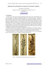
A STUDY ON THE THICKNESS HOMOGENEITY AND ...
A STUDY ON THE THICKNESS HOMOGENEITY AND ...
A STUDY ON THE THICKNESS HOMOGENEITY AND ...

Create successful ePaper yourself
Turn your PDF publications into a flip-book with our unique Google optimized e-Paper software.
Chem. Listy 99, 1234 – 2345 (2008) Titul akce.<br />
A <strong>STUDY</strong> <strong>ON</strong> <strong>THE</strong> <strong>THICKNESS</strong><br />
<strong>HOMOGENEITY</strong> <strong>AND</strong> REFRACTIVE<br />
INDEX OF THIN ORGANIC LAYERS<br />
OLDŘICH ZMEŠKAL, OTA SALYK, MICHAL VESELÝ,<br />
PETR DZIK<br />
Brno University of Technology<br />
Faculty of Chemistry, Purkynova 118, 612 00 Brno<br />
zmeskal@fch.vutbr.cz<br />
1 Introduction<br />
This paper deals with the utilization of optical and<br />
interference microscopy for the study of thin film layers. We<br />
present a new and very simple method for the determination of<br />
refractive indexes of transparent layers based on interference<br />
phenomena. Both thin layer thickness and refractive index can<br />
be determined by this method.<br />
We used this method for a complex analysis of sandwich<br />
and gap structures of organic semiconductor components (e.g.<br />
ITO/PEDOT/DPP/Alq3/Al) prepared by a combination of<br />
following procedures: vacuum vapour deposition and/or spin<br />
coating and/or inkjet printing. A series of photographs of one<br />
sample was recorded and analysed which gave us the<br />
thicknesses of individual layers, their homogeneity and their<br />
refractive indexes.<br />
Recorded images were processed by means of image<br />
analysis (correlative and fractal analysis). Image analysis was<br />
performed using application HarFA (Harmonic and Fractal<br />
Image Analyser), which has a wide potential of use not only for<br />
image analysis but for analysis of video clips, signals and<br />
numerical data as well.<br />
Results obtained by image analysis methods were<br />
confirmed and eventually further extended by ellipsometric<br />
measurements, which is unfortunately more time consuming<br />
and challenging.<br />
2 Experimental<br />
2.1 Sample preparing<br />
Within the context of development of new cheap organic<br />
materials suitable for optoelectronic applications (e.g.<br />
photovoltaic cells, light emitting diodes, etc.) new techniques<br />
of their cheap production are looked for. The preparation of<br />
thin films structures by means of various methods, e.g. spin<br />
coating, vacuum evaporation or inkjet printing seems to be<br />
very perspective techniques. Structures prepared for electronic<br />
applications are mostly multilayered with a complicated<br />
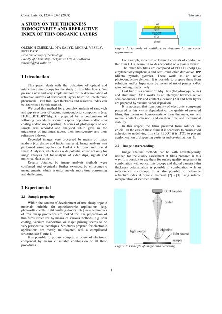
structure, see Figure 1.<br />
It is possible to prepare complex structure of electronic<br />
component by means of suitable combination of all three<br />
procedures.<br />
1<br />
Figure 1: Example of multilayered structure for electronic<br />
applications.<br />
For example, structure at Figure 1 consists of conductive<br />
thin film ITO (indium tin oxide) deposited on a glass substrate.<br />
The other two films are composed of PEDOT (poly(3,4ethylenedioxythiophene))<br />
and semi conductive derivative DPP<br />
(diketo pyrrolo pyrrole). These work as an active<br />
photoconductive element. It is possible to prepare these from<br />
solutions and/or dispersions by means of inkjet printer and/or<br />
spin coating, respectively.<br />
Last two films consist of Alq3 (tris (8-hydroxyquinoline)<br />
and aluminium. Alq3 works as an interlayer between active<br />
semiconductor DPP and contact electrode (Al) and both layers<br />
are prepared by vacuum vapor deposition.<br />
It is apparent that functionality of electronic component<br />
prepared in this way is dependent on the quality of prepared<br />
films, this means on homogeneity of their thickness, on their<br />
mutual contact (adhesion) and on their time and mechanical<br />
stability.<br />
In this respect the films prepared from solution are<br />
crucial. In the case of these films it is necessary to ensure good<br />
adhesion to underlying film (for PEDOT it is ITO), to prevent<br />
agglomeration of dispersing particles and crystallization [1].<br />
2.2 Image data recording<br />
Image analysis methods can be with advantageously<br />
utilized for the quality assessment of films prepared in this<br />
way. It is possible to use them for surface quality assessment in<br />
combination with optical microscope and digital camera. Film<br />
thickness determination is possible in combination with an<br />
interference microscope. It is also possible to determine<br />
refractive index of organic materials [2] - [3] using suitable<br />
interpretation of recorded results.<br />
Figure 2: Principle of image data recording
Chem. Listy 99, 1234 – 2345 (2008) Titul akce.<br />
For example, it is possible to use the software HarFA<br />
developed by authors of this contribution for image analysis. It<br />
is necessary to eliminate image errors caused by e.g. nonhomogeneity<br />
of the light, by non-linear transfer of brightness<br />
(gamma correction), and by thermal noise [4 - 6].<br />
Interference microscope Interphako (Carl Zeiss Jena) is<br />
used for the film thickness measurement. The principle of the<br />
measurement is based on the phase shift between beams<br />
reflected from the surface of the thin organic film and<br />
evaporated Al refractive layers. Film structure is demonstrated<br />
at Figure 3. This phase shift is in a good agreement with double<br />
thickness of the film, as demonstrated at Figure 3 (on the top).<br />
Figure 3: Principle of thickness layer measurements with using<br />
of interference microscope<br />
Using splitting and three-dimensional shift of two parts of<br />
the figure and their subsequent composition it is possible to get<br />
interferential images such as those at Figure 4.<br />
Figure 4: Interference microscope images (from the "air" side)<br />
for edge of ITO (on the left) and DPP (on the right)<br />
The details for two edges at aluminium contact are for<br />
ITO layer (on the left) and for DPP (on the right side). The<br />
shift of the interference line at the edge is in agreement with<br />
the Figure 3. A similar image can be observed from the bottom<br />
side of the sample - from the "glass" side. The results are<br />
presented at Figure 5. We can see that shift on the edge is<br />
greater than when it is observed from the "air" side of the<br />
sample (Figure 4).<br />
2<br />
Figure 5: Interference microscope images (from the "glass"<br />
side) for edge of ITO (on the left) and DPP (on the right)<br />
2.2 Data analysis<br />
The analysis performed by HarFA consists of the<br />
following steps:<br />
• Recording of image sequences (videos) of electrical<br />
contact from the side "air" and "glass (Open video, File<br />
types: Images). This step was set for more effective<br />
analysis.<br />
• Selection of interesting part of interference images, at the<br />
place of main interference maxima (the square 512 × 512<br />
pixels was selected).<br />
• Selection of proper colour space for analysis (the<br />
Brightness, not threshold - not BW settings was select).<br />
• Making of two videos (from "air" and from "glass" side)<br />
which was consist from interference image sequences<br />
(Save square video as ...)<br />
• Processing of correlation analysis for selected frames of<br />
videos. Selected part was vertical rectangle 256 × 512<br />
pixels at the frame middle (Correlation). The results were<br />
saved as images (see Figure 6) and as data files (see<br />
Figure 7).<br />
Figure 6: The results of correlation analysis - sharpen lines of<br />
the same phase on the image: the split of ITO edge from the<br />
"air" (on top) and from the "glass" (bottom) measuring.<br />
The saved data were further statistical processed by a very<br />
simple procedure. The average values of all lines were<br />
calculated and a rotation leading to horizontal zero reference<br />
line was performed. . The average shift of the split and average<br />
wavelength (in pixels) from the shift of lines was calculated.<br />
The results of these very simple calculations are at Figure 8 for<br />
ITO from "air" and "glass" side.
Chem. Listy 99, 1234 – 2345 (2008) Titul akce.<br />
Figure 7: The phase lines of the ITO edge split from the "air"<br />
side measuring.<br />
The thickness and refractive index of DPP and ITO can be<br />
immediately from these dependences determined. The results<br />
of calculations are summarized in Table I. The values were<br />
calculated as the average values of all pixels at the edge<br />
(Figure 7). The uncertainty of these values is very small; the<br />
errors are caused by the homogeneity of the measured surface.<br />
Figure 8: The corrected phase lines of the ITO edge split from<br />
the both "air" and "glass" side measuring.<br />
The thickness was calculated from the known wave length<br />
λ = 512 nm, refractive index from the simple equation<br />
n = Δs<br />
Δl<br />
, where Δs is so called optical line and Δl real line of<br />
the light. The profile of average phase line shift for the whole<br />
contact is presented on Figure 8.<br />
Figure 9: The profile of average phase line.<br />
3<br />
The imperfect groves created by cutting to DPP layer<br />
give in maxima the same shifts of phase as the second ege<br />
(DPP). The right changes of the phase are caused by<br />
inhomogeneties on the end of glass.<br />
3 Results<br />
We can see from the results at the Table 1 that the ITO<br />
layer is thinner and its homogeneity is lower than DPP layer.<br />
Also refractive index value is more accurately for ITO layer.<br />
Figure 10: The refractive index both ITO and DPP layer<br />
calculated from edge split reason.<br />
Figure 11: The thickness both ITO and DPP layer calculated<br />
from edge split reason.<br />
These results confirm the dependences of refractive<br />
indexes and thicknesses on the split position of layer edge on<br />
Figure 10 and Figure 11. We can see that the homogeneity of<br />
the ITO thickness is greater than the momogeneity of DPP and<br />
also the refractive index is more constant. The results are in<br />
agreement with data from literature [7].
Chem. Listy 99, 1234 – 2345 (2008) Titul akce.<br />
Table 1: The refractive index and thickness parameters of ITO<br />
and DPP layers (λ = 512 nm)<br />
parameter ITO layer DPP layer<br />
sample thickness (nm) 38 ± 1 80 ± 5<br />
optical thickness (nm) 66 ± 3 107 ± 18<br />
refractive index (-) 1.73 ± 0.05 1.34 ± 0.15<br />
4 Conclusions<br />
The new very simple and quick method for the<br />
determining of layer thickness and their refractive index was<br />
presented. The other advantages are that the calculation of<br />
refractive index is not dependent on the surrounding layers but<br />
only on the layer with edge. This fact is advantage in contrast<br />
to ellipsometry.<br />
5 References<br />
1. Zmeškal, O.; Veselý, M.; Vala, M.; Bednář, P.; BŽATEK,<br />
T. Image Analysis Used to Study Physical Properties of<br />
Printed Organic Thin Films. In VIII Seminar in Graphic<br />
Arts. Conference Proceedings. Pardubice, Universita<br />
Pardubice. 2007. p. 131 - 137. ISBN 978-807-1949-91-6.<br />
2. Zmeškal O., SEDLÁK O., Nežádal M.: Metody obrazové<br />
analýzy dat, Digital Imaging in Biology and Medicine, 1st<br />
ed. České Budějovice: Czech Academy of Science, 2002,<br />
p. 34–43<br />
3. Zmeškal O., Nežádal M., Sedlák O.: Využití fraktální<br />
analýzy při hodnocení kvality tisku, IV. Polygraphic<br />
Conference, University of Pardubice, September 12. – 13.,<br />
2001, p. 92 – 101<br />
4. Tomankova, K.; Jerabkova, P.; Zmeskal, O.; Vesela, M.;<br />
Haderka, J. Use of the Image Analysis to study growth and<br />
division of yeast cells. Journal of Imaging Science and<br />
Technology, 50(6), 2006. p. 583 - 589. ISSN 1062-3701,<br />
5. Jerabkova, P.; Zmeskal, O.; Haderka, J.: Fractal Analysis<br />
of Images Using Wavelet Transformation, in Complexus<br />
Mundi, WS. London, World Scientific. 2006. p. 305 - 312.<br />
ISBN 981-256-666-X<br />
6. Jerabkova P., Zmeskal O., Vesela M.: Application of<br />
Image Analysis Methods in Yeast Cell Study, Chemisrty &<br />
Life. 1st ed. FCH BUT Brno, 2005. p. s292 - s294, ISSN<br />
0009-2770 (English Version, PDF)<br />
7. Jong Kyu Kim Schubert, M.F. Xi, J.-Q. Mont, F.<br />
Schubert, E.F. Enhancement of Light Extraction in GaInN<br />
Light-Emitting Diodes with Graded-Index Indium Tin<br />
Oxide Layer. Lasers and Electro-Optics CLEO 2007,<br />
2007. ISBN 978-1-55752-834-6<br />
Acknowledgement (This work was supported by project<br />
KAN401770651 from The Academy of Sciences of the Czech<br />
4<br />
Republic and by project and by grant FT-TA/036 from the<br />
Ministry of Industry and Trade of the Czech Republic).