An Analysis Of Flash And HDD Technology Trends - Flash Memory ...
An Analysis Of Flash And HDD Technology Trends - Flash Memory ...
An Analysis Of Flash And HDD Technology Trends - Flash Memory ...

Create successful ePaper yourself
Turn your PDF publications into a flip-book with our unique Google optimized e-Paper software.
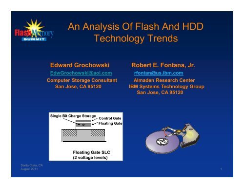
<strong>An</strong> <strong>An</strong>alysis <strong>Of</strong> <strong>Flash</strong> <strong>An</strong>d <strong>HDD</strong><br />
<strong>Technology</strong> <strong>Trends</strong><br />
Edward Grochowski Robert E. Fontana, Jr.<br />
EdwGrochowski@aol.com rfontan@us.ibm.com<br />
Computer Storage Consultant Almaden Research Center<br />
San Jose, CA 95120 IBM Systems <strong>Technology</strong> Group<br />
San Jose, CA 95120<br />
Single Bit Charge Storage<br />
e -<br />
Floating Gate SLC<br />
(2 voltage levels)<br />
Control Gate<br />
Floating Gate<br />
Santa Clara, CA<br />
August 2011 1
Introduction and Topics<br />
1. <strong>An</strong>alyze Storage<strong>Technology</strong> <strong>Trends</strong> For <strong>Flash</strong> and <strong>HDD</strong><br />
2. Project To Where These Principal Storage Technologies Will Evolve<br />
3. Discuss Concerns With These Evolutions<br />
4. Project Data Densities<br />
5. Project Costs per Gbyte<br />
6. <strong>An</strong>alyze Lithography Challenges<br />
7. Future Designs for <strong>Flash</strong>/<strong>HDD</strong><br />
Santa Clara, CA<br />
August 2011 2
Free-format slide title<br />
Exabytes Shipped/Year<br />
4000.00<br />
3500.00<br />
3000.00<br />
2500.00<br />
2000.00<br />
1500.00<br />
1000.00<br />
500.00<br />
<strong>HDD</strong><br />
NAND <strong>Flash</strong><br />
0.00<br />
2000 02 04 06 08 10 12 14<br />
100 102 104 106 108 110 112 114<br />
Ed Grochowski/Tom Coughlin<br />
TB2010Y.PRZ<br />
<strong>HDD</strong> (Ref. Coughlin/Grochowski 2010 Report)<br />
NAND <strong>Flash</strong> (Ref. John Monroe, Gartner)<br />
Production Year<br />
Santa Clara, CA<br />
August 2011 3<br />
30X
2.5 inch<br />
<strong>HDD</strong> Capacity, GBytes<br />
<strong>HDD</strong> roadmap2010B.prz<br />
10000<br />
1000<br />
100<br />
10<br />
3.5 inch form factor<br />
2.5 inch<br />
8.1 GB<br />
4 GB<br />
20 GB<br />
750GB Server 10K RPM<br />
2000 GB Desktop 7200 RPM<br />
1.8 inch<br />
1.0 inch<br />
36GB Server<br />
15K RPM<br />
1 GB<br />
1<br />
98 2000 100 102 02 104 04 106 06 108 08 2010 110 112 12 114 14<br />
Availability Year<br />
<strong>HDD</strong> CapacityRoadmap<br />
Ed Grochowski/Tom Coughlin<br />
Santa Clara, CA<br />
August 2011 4<br />
12 GB<br />
1-2TB Server<br />
10K-15K RPM<br />
10TB Desktop<br />
7200 RPM<br />
300 GB Server<br />
15K RPM 1 TB<br />
5TB<br />
Desktop/Laptop<br />
300 GB 750 GB 7200 RPM<br />
250 GB
NAND Roadmap 2011X.prz<br />
Circuit Capacity Mbits<br />
Projected NAND <strong>Flash</strong> <strong>Memory</strong> Circuit Density Roadmap<br />
1000000<br />
100000<br />
10000<br />
1000<br />
100<br />
SLC<br />
MLC<br />
Floating Gate<br />
128 Gb 15 nm est.<br />
80 Gb 24 nm<br />
64 Gb 24 nm<br />
16 Gb 45 nm<br />
8 Gb 65 nm<br />
4 Gb 90 nm<br />
2 Gb 90 nm<br />
1 Gb 130 nm<br />
512 Mb 180 nm<br />
256 Mb 250 nm<br />
64 Mb 250 nm<br />
32 Mb 400 nm<br />
16 Mb 600 nm<br />
10<br />
1990 1995 2000 2005 2010 2015 2020<br />
Production Year<br />
Charge Trap<br />
Advanced<br />
<strong>Technology</strong><br />
Santa Clara, CA<br />
August 2011 5
Free-format slide title<br />
areal2011egA.prz<br />
Areal Density GIgabits/in2<br />
10 1E+7 104 4<br />
1E+6 103<br />
10 3<br />
1E+5 102 10 2<br />
1E+4 10<br />
10 1<br />
1E+3 1<br />
1<br />
1E+2<br />
10 -1<br />
10-1<br />
10 1E+1<br />
-2<br />
10-2<br />
<strong>HDD</strong>/<strong>Flash</strong> Areal Density Perspective<br />
1st MR Head<br />
<strong>HDD</strong><br />
Products<br />
<strong>Flash</strong><br />
Products<br />
1st GMR Head<br />
60% CGR<br />
16MB<br />
1st AFC Media<br />
100% CGR<br />
64MB<br />
Perpendicular<br />
Recording<br />
90 95 100 2000 2005 105 110 2010 115 2015<br />
Production Year<br />
TMR Head<br />
40% CGR<br />
4K Sector<br />
Region<br />
Copyright Ed Grochowski<br />
Santa Clara, CA<br />
August 2011 6<br />
256MB<br />
512MB<br />
1 GB<br />
2 GB<br />
4 GB<br />
8 GB<br />
8 GB 20nm<br />
64 GB (3 MLC ?)<br />
32 GB (2 MLC)<br />
16 GB (2 MLC)
Price/GByte, Dollars<br />
oemprc2009a.prz<br />
100000<br />
Price $/GB<br />
oemprc2011B.prz<br />
10000<br />
1000<br />
100<br />
10<br />
1<br />
0.1<br />
0.01<br />
Ed Grochowski<br />
DRAM/<strong>Flash</strong><br />
Enterprise <strong>HDD</strong><br />
Desktop <strong>HDD</strong><br />
Average Retail Prices of Storage<br />
Mobile <strong>HDD</strong><br />
1990 1995 2000 2005 2010 2015<br />
Year<br />
DRAM<br />
<strong>Flash</strong><br />
Desktop<br />
Mobile<br />
Enterprise<br />
1"<br />
32 GB <strong>Flash</strong><br />
Santa Clara, CA<br />
August 2011 7<br />
1 " <strong>HDD</strong><br />
750 GB Desktop<br />
1.5TB Desktop<br />
2TB Desktop<br />
3 TB Desktop<br />
300 GB/15K Server<br />
500 GB Mobile Drive
Magnetic Recording Cell<br />
• The unique attribute of the magnetic bit cell in a hard disk drive<br />
(<strong>HDD</strong>) is that the bits are unpatterned tremendous cost<br />
advantage<br />
• The bit length is “sub lithographic”<br />
• Bits are “magnetically” templated into the media using a single photo<br />
lithographically defined magnetic transducer<br />
• Bit width is determined by the lithography used to form the write<br />
transducer. The smallest lithographically defined feature in the<br />
magnetic head is the read transducer ~ ½ Track Pitch = F<br />
• Bit length is determined without lithography! It is sub lithographic! It<br />
is defined by the distance the disk rotates during the time interval<br />
that alternating current pulses are applied to the write yoke.<br />
• Bit length is limited by the resolution of the sensor, i.e. the read gap<br />
with dimensions G determined by depositions, not lithography<br />
• <strong>An</strong> <strong>HDD</strong> Product Example (635 Gbit/in² Areal Density)<br />
– Minimum Lithography 37 nm = F<br />
Santa Clara, CA<br />
August 2011 – Bit Cell 74 nm x 13 nm<br />
8<br />
– Smallest Bit Feature 13 nm ~ 33% F, ~ 50% IC F
Three Major <strong>HDD</strong> Innovations<br />
Santa Clara, CA<br />
August 2011 9
<strong>HDD</strong> Shingled Write<br />
1. Is A Band <strong>Technology</strong>, Not A Sector Or Track (Marginally)<br />
2. Ideally Suited For Streaming Applications (>>Gbyte<br />
Movies)<br />
3. Many Potential Ideas For Writing Tracks<br />
4. Requirement For Correct Choices On Buffer Tracks <strong>An</strong>d<br />
Band Sizes<br />
5. Involves Rewriting On Disk Or Buffer electronics Within<br />
Drive<br />
6. If Changes To OS Or System Electronics, Delays Are<br />
Probable, If Drop-in <strong>Technology</strong>, Applications Will Arrive<br />
Soon<br />
Santa Clara, CA<br />
August 2011 10
Surface Dimensions<br />
(Chip or Disk)<br />
Cell Size Comparison<br />
8GB NAND <strong>Flash</strong> 8GB NAND <strong>Flash</strong> 375 GB 1 surface <strong>HDD</strong><br />
16.5 mm x 10.1 mm 12.5 mm x 9.5 mm 87.0 mm disk diameter<br />
24.0 mm hub diameter<br />
1.5 mm edge exclusions<br />
<strong>Memory</strong> Surface Area 167 mm² 118 mm² 5491 mm²<br />
Active <strong>Memory</strong> Area ~ 122 mm² (73%) ~ 71 mm² (65%) ~ 4969 mm² (90%)<br />
Minimum Lithography F = 25 nm F = 20 nm F = 37 nm<br />
Active Bit Cell Area 1906 nm² = 3.0 F² 1109 nm² = 2.8 F² 981 nm² = 0.7 F²<br />
Bit Cell Dimension 44 nm x 44 nm 33 nm x 33 nm 74 nm x 13 nm<br />
Maximum Areal Density 330 Gb/in² 560 Gb/in² 635 Gb/in²<br />
Santa Clara, CA<br />
August 2011 11
Lithography and NAND <strong>Flash</strong><br />
• Typical NAND cells formed with sub 30 nm lithography with Intel-<br />
Micron providing leading edge devices at 25 nm to 20 nm<br />
• Bit cell area approaches 2.5 F² (F is the minimum lithographic feature)<br />
for Self Aligned STI multi level (2 bit per cell) designs<br />
• <strong>HDD</strong> cells formed with minimum features close to DRAM<br />
requirements<br />
• Patterned Media cells will require substantial “invention” in lithography<br />
to meet density goals<br />
Multi Level NAND Cell<br />
Santa Clara, CA<br />
August 2011 12
MTBF2011B.prz<br />
MTBF Specifications<br />
Enterprisebased<br />
<strong>Flash</strong><br />
As specified MTBF, khrs.<br />
2200<br />
2000<br />
1800<br />
1600<br />
1400<br />
1200<br />
1000<br />
800<br />
600<br />
400<br />
200<br />
Ed Grochowski<br />
Industry <strong>HDD</strong> MTBF Specifications<br />
0<br />
1985 1990 1995 2000 2005 2010 2015 2020<br />
Product Ship Date<br />
Consumer-based <strong>Flash</strong><br />
Santa Clara, CA<br />
August 2011 13<br />
<strong>HDD</strong>
<strong>Flash</strong> Scaling<br />
<strong>Flash</strong>chal2011B.prz<br />
No. Electrons per Vt Shift<br />
10000<br />
1000<br />
100<br />
10<br />
1<br />
Lithography nm<br />
130 90 64 51 40 32 20 18 16 14 12<br />
FG <strong>Flash</strong> Electrical Scaling Challenges<br />
<strong>Flash</strong> Chip Capacity (GBytes)<br />
Based on Chung Lam (IBM Research)<br />
0.08 0.12 0.25 0.50 1.0 2.0 4.0 8.0 16.0 25.0 64.0 120.0<br />
2000 2005 2010 2015 2020<br />
Santa Clara, CA<br />
August 2011 14<br />
Year
New Transistor Designs<br />
Santa Clara, CA<br />
August 2011 15
<strong>Flash</strong> Scaling Challenges<br />
1. >15 nm Lithography (EUV <strong>Technology</strong> Too<br />
Expensive For <strong>Flash</strong>, Also <strong>HDD</strong>)<br />
2. Fewer Electrons >> 100 (Leakage >1 Electron<br />
Per Month)<br />
3. Electric Field Stress During Programming Too<br />
High<br />
4. Write Endurance Degrades<br />
Santa Clara, CA<br />
August 2011 16
Conclusion<br />
1. Expect Significantly Reduced Scaling <strong>An</strong>d Capacity<br />
Progress- <strong>Flash</strong> <strong>An</strong>d <strong>HDD</strong>-In Future<br />
2. New Processing <strong>An</strong>d Structural Techniques Limited<br />
By Implementation Costs<br />
3. Storage Requirements Will Continue Vigorous<br />
Demands For Both <strong>Flash</strong> <strong>An</strong>d <strong>HDD</strong> Products<br />
4. Door Is Open For Alternative Technologies (FeRam,<br />
MRAM Are Imbedded Technologies; PCM Is<br />
Crosspoint)<br />
Santa Clara, CA<br />
August 2011 17