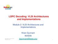
LDPC Decoding: VLSI Architectures and Implementations
LDPC Decoding: VLSI Architectures and Implementations
LDPC Decoding: VLSI Architectures and Implementations

Create successful ePaper yourself
Turn your PDF publications into a flip-book with our unique Google optimized e-Paper software.
<strong>LDPC</strong> <strong>Decoding</strong>: <strong>VLSI</strong> <strong>Architectures</strong><br />
<strong>and</strong> <strong>Implementations</strong><br />
Module 2: <strong>VLSI</strong> <strong>Architectures</strong> <strong>and</strong><br />
<strong>Implementations</strong><br />
Kiran Gunnam<br />
NVIDIA<br />
kgunnam@ieee.org<br />
Flash Memory Summit 2013<br />
Santa Clara, CA 1
Outline<br />
• Check Node Unit Design<br />
• Non-layered Decoder Architecture<br />
- Block Serial Processing<br />
- From Throughput requirements to design specifications<br />
• Layered Decoder Architecture<br />
- Block Serial Processing<br />
- Block Serial Processing <strong>and</strong> scheduling for Irregular H<br />
matrices<br />
- Block Parallel Processing<br />
- From Throughput requirements to design specifications<br />
• Case Study of Decoders for 802.11n <strong>and</strong> Flash<br />
Channel<br />
Flash Memory Summit 2013<br />
Santa Clara, CA 2
<strong>LDPC</strong> <strong>Decoding</strong>, Quick Recap 1/5<br />
Bit nodes (also called variable nodes) correspond to received bits.<br />
Check nodes describe the parity equations of the transmitted bits.<br />
eg. v1+v4+v7= 0; v2+v5+v8 =0 <strong>and</strong> so on.<br />
The decoding is successful when all the parity checks are satisfied (i.e. zero).<br />
Flash Memory Summit 2013<br />
Santa Clara, CA 3
<strong>LDPC</strong> <strong>Decoding</strong>, Quick Recap 2/5<br />
• There are four types of LLR messages<br />
• Message from the channel to the n-th bit node,<br />
( i )<br />
Q − ><br />
( )<br />
• Message from n-th bit node to the m-th check node n m or simply<br />
L n<br />
( i )<br />
Q nm<br />
i<br />
R − ><br />
• Message from the m-th check node to the n-th bit node m n or simply<br />
• Overall reliability information for n-th bit-node<br />
m = 0<br />
m = 1<br />
m = 2<br />
P n<br />
( i )<br />
R m n<br />
(i)<br />
R0 −>3<br />
R<br />
(i)<br />
2 −>3<br />
( i)<br />
Q<br />
3 > 1<br />
−<br />
6<br />
n = 0 n = 1 n = 2 n = 3 n = 4 n = 5 n = 6<br />
P<br />
L 3<br />
Channel Detector<br />
4
<strong>LDPC</strong> <strong>Decoding</strong>, Quick Recap 3/5<br />
Notation used in the equations<br />
x is the transmitted bit n ,<br />
n<br />
L is the initial LLR message for a bit node (also called as variable node) n ,<br />
n<br />
n<br />
received from channel/detector<br />
P is the overall LLR message for a bit node n ,<br />
x ) n<br />
is the decoded bit n (hard decision based on P n<br />
) ,<br />
[Frequency of P <strong>and</strong> hard decision update depends on decoding schedule]<br />
Μ (n) is the set of the neighboring check nodes for variable node n ,<br />
Ν(m)<br />
is the set of the neighboring bit nodes for check node m .<br />
For the i th iteration,<br />
( i)<br />
Q<br />
nm<br />
is the LLR message from bit node n to check node m ,<br />
( i )<br />
R<br />
mn<br />
is the LLR message from check node m to bit node n .<br />
Flash Memory Summit 2013<br />
Santa Clara, CA 5<br />
5
<strong>LDPC</strong> <strong>Decoding</strong>, Quick Recap 4/5<br />
(A) check node processing: for each m <strong>and</strong> n Ν(m)<br />
R<br />
κ<br />
( i)<br />
mn<br />
∈ ,<br />
( i) ( i) ( i)<br />
= δ κ<br />
(1)<br />
mn<br />
mn<br />
= R =<br />
mn<br />
( )<br />
( i − )<br />
min Q<br />
n′∈ Ν m \ n n ′ m<br />
( i) 1<br />
mn<br />
The sign of check node message<br />
(2)<br />
( i )<br />
R is defined as<br />
mn<br />
( )<br />
⎛<br />
( )<br />
⎞<br />
i<br />
i−1<br />
δmn<br />
= ⎜<br />
⎟<br />
⎝ n′∈Ν<br />
( m)<br />
\ n ⎠<br />
( i)<br />
whereδ takes value of + 1 or − 1<br />
sgn ( Q )<br />
(3)<br />
∏ n′<br />
m<br />
mn<br />
Flash Memory Summit 2013<br />
Santa Clara, CA 6
<strong>LDPC</strong> <strong>Decoding</strong>, Quick Recap 5/5<br />
(B) Variable-node processing: for each n <strong>and</strong> m M ( n)<br />
( i) ( i)<br />
Q = L + ∑ R ′<br />
(4)<br />
nm n m n<br />
m′∈Μ<br />
( n)\<br />
m<br />
(C) P Update <strong>and</strong> Hard Decision<br />
( i)<br />
P = L + ∑ R<br />
(5)<br />
n n mn<br />
m∈M ( n)<br />
∈ :<br />
A hard decision is taken where x ˆn<br />
= 0 if Pn<br />
≥ 0 , <strong>and</strong> x ˆn<br />
= 1 if P<br />
n<br />
< 0 .<br />
T<br />
If xˆ nH = 0 , the decoding process is finished with x ˆn<br />
as the decoder output;<br />
otherwise, repeat steps (A) to (C).<br />
If the decoding process doesn’t end within some maximum iteration, stop <strong>and</strong><br />
output error message.<br />
Scaling or offset can be applied on R messages <strong>and</strong>/or Q messages for better<br />
performance.<br />
Flash Memory Summit 2013<br />
Santa Clara, CA 7
On-the-fly Computation<br />
Our previous research introduced the following concepts to <strong>LDPC</strong> decoder implementation<br />
[1-10] presented at various IEEE conferences. ICASSP’04,Asilomar’06,<strong>VLSI</strong>’07,ISWPC’07,<br />
ISCAS’07, ICC’07, Asilomar’08. References P1 <strong>and</strong> P2 are more comprehensive <strong>and</strong> are<br />
the basis for this presentation.<br />
1. Block serial scheduling<br />
2. Value-reuse,<br />
3. Scheduling of layered processing,<br />
4. Out-of-order block processing,<br />
5. Master-slave router,<br />
6. Dynamic state,<br />
7. Speculative Computation<br />
8. Run-time Application Compiler [support for different <strong>LDPC</strong> codes with in a class of codes.<br />
Class:802.11n,802.16e,Array, etc. Off-line re-configurable for several regular <strong>and</strong> irregular<br />
<strong>LDPC</strong> codes]<br />
All these concepts are termed as On-the-fly computation as the core of these<br />
concepts are based on minimizing memory <strong>and</strong> re-computations by employing just<br />
in-time scheduling. For this presentation, we will focus on concepts 1-4.<br />
Flash Memory Summit 2013<br />
Santa Clara, CA 8
Check Node Unit (CNU) Design<br />
( i)<br />
i<br />
i −<br />
κ →<br />
= →<br />
= min<br />
( )<br />
( )<br />
R Q<br />
l′∈ Ν m \ l l ′ → m<br />
( ) 1<br />
m l m l<br />
bits to checks<br />
m<br />
checks to bits<br />
m<br />
i<br />
Q n1 −> m<br />
= −10<br />
i<br />
i<br />
Q −> m<br />
13<br />
Q n<br />
n 2−><br />
=<br />
m<br />
−5<br />
L 1 L 2 L 3<br />
3<br />
=<br />
i<br />
i<br />
R −> -5<br />
= i<br />
−> n2 -10 R m −> n 5<br />
m<br />
= n1 R m<br />
L 1 L 2 L 3<br />
3 =<br />
Flash Memory Summit 2013<br />
Santa Clara, CA 9<br />
9
κ<br />
Check Node Unit (CNU) Design<br />
( i)<br />
mn<br />
The above equation (2) can be reformulated as the following set of<br />
equations.<br />
( i)<br />
M1m<br />
= min<br />
n′∈ Ν<br />
( i)<br />
( m)<br />
( m)<br />
( i −1)<br />
Q mn ′<br />
( i −1)<br />
M 2m<br />
= 2nd min Q<br />
n′∈ Ν mn ′<br />
• Simplifies the number of comparisons required as well as the memory<br />
needed to store CNU outputs.<br />
• Additional possible improvements: The correction has to be applied to only two<br />
values instead of distinct values. Need to apply 2’s complement to only 1 or 2 values<br />
instead of values at the output of CNU.<br />
Flash Memory Summit 2013<br />
Santa Clara, CA 10<br />
10<br />
(6)<br />
(7)<br />
k = Min1Index<br />
(8)<br />
( i) ( i)<br />
mn<br />
M1<br />
κ = , ∀ n ∈ Ν( m) \ k<br />
m<br />
( )<br />
( i − )<br />
= R = min Q<br />
n′∈ Ν m \ n n ′ m<br />
( i) 1<br />
mn<br />
( )<br />
= M 2 i m<br />
, n = k<br />
(9)<br />
(2)
CNU Micro Architecture for minsum<br />
Flash Memory Summit 2013<br />
Santa Clara, CA 11
VNU Micro Architecture<br />
Flash Memory Summit 2013<br />
Santa Clara, CA 12
Example QC-<strong>LDPC</strong> Matrix<br />
H<br />
=<br />
⎡I<br />
⎢<br />
⎢<br />
I<br />
⎢I<br />
⎢<br />
⎢:<br />
⎢<br />
⎣I<br />
I<br />
σ<br />
2<br />
σ<br />
σ<br />
c−1<br />
σ<br />
I<br />
2<br />
σ<br />
4<br />
σ<br />
( c−1)2<br />
...<br />
...<br />
...<br />
...<br />
σ<br />
σ<br />
σ<br />
I<br />
r−1<br />
2( r−1)<br />
( c−1)(<br />
r−1)<br />
⎤<br />
⎥<br />
⎥<br />
⎥<br />
⎥<br />
⎥<br />
⎥<br />
⎦<br />
⎡0<br />
⎢<br />
⎢<br />
1<br />
σ = ⎢0<br />
⎢<br />
⎢:<br />
⎢<br />
⎣0<br />
0<br />
0<br />
1<br />
0<br />
...<br />
...<br />
...<br />
...<br />
0<br />
0<br />
.0<br />
.1<br />
1⎤<br />
0<br />
⎥<br />
⎥<br />
0⎥<br />
⎥<br />
⎥<br />
0⎥<br />
⎦<br />
Example H Matrix, Array<br />
<strong>LDPC</strong><br />
r row/ check node degree=5<br />
c columns/variable node degree=3<br />
Sc circulant size=7<br />
N=Sc*r=35<br />
Flash Memory Summit 2013<br />
Santa Clara, CA 13
Example QC-<strong>LDPC</strong> Matrix<br />
S 3 × 5<br />
⎡2<br />
3 110 142 165⎤<br />
=<br />
⎢<br />
⎥<br />
⎢<br />
5 64 96 113 144<br />
⎥<br />
⎢⎣<br />
7 50 75 116 174⎥⎦<br />
Example H Matrix<br />
r row degree=5<br />
c column degree =3<br />
Sc circulant size=211<br />
N=Sc*r=1055
Non-Layered Decoder Architecture<br />
Supported H matrix<br />
parameters<br />
r row degree=36<br />
c column degree =4<br />
L Memory=> Depth 36, Width=128*5<br />
HD Memory=> Depth 36, Width=128<br />
Possible to remove the shifters (light-blue) by rearranging<br />
H matrix’s first layer to have zero shift<br />
Sc ciruclant size=128<br />
coefficients.<br />
Flash Memory Summit 2013<br />
N=Sc*r=4608<br />
Santa Clara, CA 15
Pipeline for NLD
Non-Layered Decoder Architecture<br />
for Array <strong>LDPC</strong> codes<br />
PS out12<br />
FS out1<br />
Q initial<br />
Q<br />
CNU1<br />
CNU2<br />
R<br />
CNU61<br />
Q 1,1<br />
R 1,1<br />
CNU<br />
Array<br />
Block<br />
Row 1<br />
Q 61,1<br />
Q 1,2<br />
CNU<br />
Array<br />
Block<br />
Q 61,2 Row 2<br />
Q 61,1<br />
Q 1,3<br />
CNU<br />
Array Q 61,2<br />
Block<br />
Q 61,3<br />
Row 3<br />
R 2,1<br />
R 61,1<br />
Q<br />
PS out92<br />
2<br />
22<br />
PS<br />
PS in<br />
in FS in<br />
2<br />
Q CNU62 R<br />
Q CNU63 R<br />
PS ou FS<br />
R ou<br />
t t FS out6<br />
PS ou FS ou<br />
t t<br />
PS out62<br />
FS<br />
PS out6<br />
out93<br />
2<br />
PS<br />
PS in<br />
in FS in<br />
2<br />
PS out63<br />
3<br />
PS out12<br />
PS<br />
FS out1<br />
out91<br />
1<br />
21<br />
PS<br />
PS in<br />
in FS in<br />
2<br />
Q CNU122 R<br />
PS ou FS ou<br />
t t<br />
PS out12<br />
FS out122<br />
2<br />
VNU 1<br />
VNU 2<br />
VNU 61<br />
Q 1,1<br />
Q 1,2Q1,3<br />
Q<br />
Q 61,1Q61,2<br />
PS out18 PS out18<br />
FS<br />
2<br />
out182<br />
3<br />
PS<br />
PS in<br />
in FS in<br />
2<br />
Q CNU123 R<br />
PS ou FS ou<br />
PS out18 PS out12 FS out1<br />
PS<br />
t t<br />
out12<br />
FS out1 3 3 83<br />
3<br />
23<br />
PS<br />
PS in<br />
in FS in<br />
2<br />
Q CNU124<br />
PS ou FS<br />
R<br />
ou<br />
PS out12<br />
PS out12 t t<br />
4<br />
FS out124<br />
3<br />
PS<br />
PS in<br />
in FS in<br />
2<br />
Q CNU125<br />
PS ou<br />
FS ou<br />
R<br />
PS out12<br />
t<br />
t<br />
5 FS out125<br />
Q 61,3<br />
PS out18<br />
PS out18<br />
FS out183<br />
3 2<br />
PS<br />
PS in<br />
in FS in<br />
2<br />
Q CNU183 R<br />
PS ou FS ou<br />
t t<br />
PS out18<br />
FS out18<br />
3<br />
3<br />
R<br />
Supported H matrix<br />
parameters<br />
r row degree=32<br />
c column degree =3<br />
Sc ciruclant size=61<br />
N=Sc*r=1952<br />
Flash Memory Summit 2013<br />
Santa Clara, CA 17
From Throughput Requirements to<br />
Design Specification<br />
• Requirements<br />
- Throughput in bits per sec.<br />
- BER<br />
- Latency<br />
• BER would dictiate Number of Iterations <strong>and</strong> degree profile(check node<br />
degrees <strong>and</strong> variable node degrees).<br />
• Circulant Size (Sc)<br />
• Number of Columns processed in one clock (Nc)<br />
• Number of bits processed per clock=Throughput/clock frequency<br />
• Sc*Nc=Nb*Iterations<br />
• Sc is usually set to less than 128 for smaller router.<br />
Flash Memory Summit 2013<br />
Santa Clara, CA 18
Layered Decoder Architecture<br />
Optimized Layered <strong>Decoding</strong> with algorithm transformations for reduced memory <strong>and</strong> computations<br />
r<br />
R<br />
r<br />
r<br />
(0)<br />
(0)<br />
l, n<br />
0,<br />
Pn<br />
= Ln<br />
= [Initialization for each new received data frame], (9)<br />
∀ i = 1,2,<br />
L,<br />
it [Iteration loop],<br />
max<br />
∀ l = 1,2, L , j [Sub-iteration loop],<br />
∀ n = 1,2,<br />
L,k<br />
[Block column loop],<br />
r<br />
( )<br />
S ( l,<br />
n)<br />
r S ( l,<br />
n)<br />
r<br />
i<br />
i−1<br />
Q = P − R<br />
( )<br />
[<br />
l,<br />
n<br />
] [<br />
n<br />
]<br />
l,<br />
n<br />
r r S<br />
R ([ ] ( l,<br />
n′<br />
)<br />
l , n<br />
l,<br />
n<br />
L,<br />
)<br />
, (10)<br />
( i) ( i)<br />
= f Q ′ , ∀n′<br />
= 1,2, k , (11)<br />
r S ( l,<br />
n)<br />
r<br />
( i)<br />
S ( l,<br />
n)<br />
r<br />
( i)<br />
[ ] [ Q ] + R<br />
P<br />
n<br />
l,<br />
n<br />
l,<br />
n<br />
where the vectors<br />
= , (12)<br />
r<br />
( i )<br />
<strong>and</strong><br />
R<br />
l , n<br />
r<br />
( i)<br />
Q<br />
l , n<br />
represent all the R <strong>and</strong> Q messages in each<br />
p × p block of the H matrix,<br />
s( l, n ) denotes the shift coefficient for the block in l th block row <strong>and</strong> n th block column of the H matrix.<br />
( i)<br />
S ( l,<br />
n<br />
Q r r<br />
denotes that the vector<br />
( i)<br />
is cyclically shifted up by the amount s( l, n )<br />
[ ]<br />
)<br />
l,<br />
n<br />
Q<br />
l , n<br />
k is the check-node degree of the block row.<br />
A negative sign on s( l, n ) indicates that it is a cyclic down shift (equivalent cyclic left shift).<br />
(⋅)<br />
f denotes the check-node processing, which embodiments implement using, for example, a Bahl-Cocke-<br />
Jelinek-Raviv algorithm (“BCJR”) or sum-of-products (“SP”) or Min-Sum with scaling/offset.<br />
Flash Memory Summit 2013<br />
Santa Clara, CA 19
Layered Decoder Architecture<br />
Our work proposed this for H matrices with regular<br />
mother matrices.<br />
Compared to other work, this work has several advantages<br />
1) No need of separate memory for P.<br />
2) Only one shifter instead of 2 shifters<br />
3) Value-reuse is effectively used for both Rnew <strong>and</strong> Rold<br />
4) Low complexity data path design-with no redundant data<br />
Path operations.<br />
5) Low complexity CNU design.<br />
r<br />
R<br />
( i)<br />
l,<br />
n<br />
=<br />
⎛<br />
f ⎜<br />
⎜<br />
⎝<br />
r<br />
[<br />
( )<br />
] ( ′<br />
i<br />
S l,<br />
n<br />
Q<br />
) ⎟ ⎟ ⎞<br />
l,<br />
n′<br />
,<br />
∀ n′<br />
= 1,2, L,<br />
k⎠<br />
r<br />
[<br />
( )] [ ]<br />
i<br />
S ( l,<br />
n)<br />
S ( l,<br />
n)<br />
( i−1)<br />
Q = P − R<br />
l,<br />
n<br />
r<br />
n<br />
r<br />
l,<br />
n<br />
r<br />
r ( r<br />
P<br />
n<br />
l,<br />
n<br />
l,<br />
n<br />
[ ]<br />
S l,<br />
n)<br />
[<br />
( )] i<br />
S ( l,<br />
n)<br />
( i)<br />
= Q + R<br />
Q=P-Rold<br />
Flash Memory Summit 2013<br />
Santa Clara, CA 20
Data Flow Diagram<br />
Flash Memory Summit 2013<br />
Santa Clara, CA 21
Data Flow<br />
Flash Memory Summit 2013<br />
Santa Clara, CA 22<br />
Parameters used here: r row degree=25, c column degree =3
Irregular QC-<strong>LDPC</strong> H Matrices<br />
Different base matrices to support different rates.<br />
Different expansion factors (z) to support multiple lengths.<br />
All the shift coefficients for different codes for a given rate are obtained from the<br />
same base matrix using modulo arithmetic<br />
Flash Memory Summit 2013<br />
Santa Clara, CA 23
Irregular QC-<strong>LDPC</strong> H Matrices<br />
Flash Memory Summit 2013<br />
Santa Clara, CA 24
Irregular QC-<strong>LDPC</strong> H Matrices<br />
<br />
<br />
<br />
<br />
<br />
Existing implementations show that these are more complex to<br />
implement.<br />
These codes have the better BER performance <strong>and</strong> selected for IEEE<br />
802.16e <strong>and</strong> IEEE 802.11n.<br />
It is anticipated that these type of codes will be the default choice for<br />
most of the st<strong>and</strong>ards.<br />
We show that with out-of-order processing <strong>and</strong> scheduling of layered<br />
processing, it is possible to design very efficient architectures.<br />
The same type of codes can be used in storage applications<br />
(holographic, flash <strong>and</strong> magnetic recording) if variable node degrees of<br />
2 <strong>and</strong> 3 are avoided in the code construction for low error floor<br />
Hocevar, D.E., "A reduced complexity decoder architecture via layered decoding of <strong>LDPC</strong> codes,"<br />
IEEE Workshop on Signal Processing Systems, 2004. SIPS 2004. .pp. 107- 112, 13-15 Oct. 2004<br />
Flash Memory Summit 2013<br />
Santa Clara, CA 25
Layered Decoder Architecture<br />
Our work proposed this for H matrices with irregular mother matrices.<br />
Compared to other work, this work has several advantages<br />
1) Q memory (some times we call this as LPQ memory) can be used to store L/Q/P instead of 3 separate memoriesmemory<br />
is managed at circulant level as at any time for a given circulant we need only L or Q or P.<br />
2) Only one shifter instead of 2 shifters<br />
3) Value-reuse is effectively used for both Rnew <strong>and</strong> Rold<br />
4) Low complexity data path design-with no redundant data<br />
Path operations.<br />
5) Low complexity CNU design.<br />
6) Out-of-order processing at both layer <strong>and</strong> circulant level for all the processing steps such as Rnew <strong>and</strong> PS processing<br />
to eliminate the pipeline <strong>and</strong> memory access stall cycles.<br />
Flash Memory Summit 2013<br />
Santa Clara, CA 26
Data Flow Diagram<br />
Flash Memory Summit 2013<br />
Santa Clara, CA 27
Illustration for out-of-order processing<br />
Rate 2/3 code. 8 Layers, 24 block columns. dv, column weight varies from 2 to 6. dc, row weight is 10 for all the layers.<br />
The following are the parameters of the circulant 1508 marked with the circle (denote this as the specified circulant):<br />
The specified circulant 1508 belongs to 3rd layer.<br />
This is the first non-zero circulant in this layer. So, the block number bn for the specified circulant 1508 is 1.<br />
The circulant index ci for this specified circulant 1508 is 21.<br />
The block column bc for this specified circulant 1508 is 3.<br />
This specified circulant 1508 takes the updated P message from the circulant 1506 marked with the rectangle. So, circulant 1506 is the dependent<br />
circulant of the circulant 1508. The dependent circulant 1506 has a circulant index ci of 11. So, the dependent circulant index dci of the circulant<br />
1508 is 11.<br />
The layer of the dependent circulant 1506 is 2. So the dependent layer dl of the circulant 1508 marked with the circle is 2.<br />
The block number of the dependent circulant 1506 is 1. So, the dependent block number db of the specified circulant 1508 is 1<br />
The shift coefficient of the specified circulant 1508 is 12. Thus, the shift matrix coefficient sm of the specified circulant 1508 is 12. The H matrix<br />
has a circulant (i.e. identity matrix of size 96 x 96 that is cyclically shifted right by the amount 12) corresponding to 12 entry 1508 in the S matrix.<br />
Note that a non-zero circulant in the H matrix corresponds to 1 entry in the H b matrix.<br />
The shift coefficient of the dependent circulant 1506 is 1. So, the delta shift matrix coefficient dsm of the specified circulant 1508 is 12-1=11.<br />
The specified circulant 1508 is the second non-zero circulant in the 3rd block column. Since the specified circulant 1508 is NOT the first non-zero<br />
circulant in its block column, the specified circulant takes the updated P message from the dependent circulant 1506 in all the iterations. Therefore,<br />
the use channel value flag ucvf of the specified circulant 1508 is 0.<br />
Flash Memory Summit 2013<br />
Santa Clara, CA 28
Illustration for out-of-order processing<br />
Rate 2/3 code. 8 Layers, 24 block columns. dv, column weight varies from 2 to 6. dc, row weight is 10 for all the layers.<br />
Non-zero circulants are numbered from 1 to 80. No layer re-ordering in processing. Out-of-order processing for Rnew. Out-of-order processing for<br />
Partial state processing.<br />
Illustration for 2 nd iteration with focus on PS processing of 2 nd layer.<br />
Rold processing is based on the circulant order 11 16 17 18 20 12 13 14 15 19 <strong>and</strong> is indicated in green.<br />
Rnew is based on the circulant order 72 77 78 58 29 3 5 6 8 10 <strong>and</strong> is indicated in blue.<br />
Q memory, HD memory access addresses are based on the block column index to which the green circulants are connected to.<br />
Q sign memory access address is based on green circulant number.<br />
Superscript indicates the clock cycle number counted from 1 at the beginning of layer 2 processing.<br />
Flash Memory Summit 2013<br />
Santa Clara, CA 29
Out-of-order layer processing for R<br />
Selection<br />
Normal practice is to compute R new messages for each layer after CNU PS processing.<br />
However, here we decoupled the execution of R new messages of each layer with the execution of corresponding<br />
layer’s CNU PS processing. Rather than simply generating Rnew messages per layer, we compute them on basis<br />
of circulant dependencies.<br />
R selection is out-of-order so that it can feed the data required for the PS processing of the second layer. For<br />
instance Rnew messages for circulant 29 which belong to layer 3 are not generated immediately after layer 3<br />
CNU PS processing .<br />
Rather, Rnew for circulant 29 is computed when PS processing of circulant 20 is done as circulant 29 is a<br />
dependent circulant of circulant of 20.<br />
Similarly, Rnew for circulant 72 is computed when PS processing of circulant 11 is done as circulant 72 is a<br />
dependent circulant of circulant of 11.<br />
Here we execute the instruction/computation at precise moment when the result is needed!!!<br />
Flash Memory Summit 2013<br />
Santa Clara, CA 30
Out-of-order block processing for<br />
Partial State<br />
Re-ordering of block processing . While processing the layer 2,<br />
the blocks which depend on layer 1 will be processed last to allow for the pipeline latency.<br />
In the above example, the pipeline latency can be 5.<br />
The vector pipeline depth is 5.so no stall cycles are needed while processing the layer 2 due to the pipelining. [In<br />
other implementations, the stall cycles are introduced – which will effectively reduce the throughput by a huge<br />
margin.]<br />
Also we will sequence the operations in layer such that we process the block first that has dependent data<br />
available for the longest time.<br />
This naturally leads us to true out-of-order processing across several layers. In practice we wont do out-of-order<br />
partial state processing involving more than 2 layers.<br />
Flash Memory Summit 2013<br />
31<br />
Santa Clara, CA 31
Overview of Schedule Optimization<br />
• The decoder hardware architecture is proposed to support out-of-order processing to<br />
remove pipeline <strong>and</strong> memory accesses or to satisfy any other performance or hardware<br />
constraint. Remaining hardware architectures won't support out-of-order processing<br />
without further involving more logic <strong>and</strong> memory.<br />
For the above hardware decoder architecture, the optimization of decoder schedule<br />
belongs to the class of NP-complete problems. So there are several classic optimization<br />
algorithms such as dynamic programming that can be applied. We apply the following<br />
classic approach of optimal substructure.<br />
• Step 1: We will try different layer schedules(j! i.e j factorial of j if there are j layers).<br />
• Step 2:Given a layer schedule or a re-ordered H matrix, we will optimize the processing<br />
schedule of each layer. For this, we use the classic approach of optimal substructure i.e.<br />
the solution to a given optimization problem can be obtained by the combination of<br />
optimal solutions to its sub problems. So first we optimize the processing order to<br />
minimize the pipeline conflicts. Then we optimize the resulting processing order to<br />
minimize the memory conflicts. So for each layer schedule, we are measuring the<br />
number of stall cycles (our cost function).<br />
• Step 3: We choose a layer schedule which minimizes the cost function i.e. meets the<br />
requirements with less stall cycles due to pipeline conflicts <strong>and</strong> memory conflicts <strong>and</strong> also<br />
minimizes the memory accesses (such as FS memory accesses to minimize the number<br />
of ports needed <strong>and</strong> to save the access power <strong>and</strong> to minimize the more muxing<br />
requirement <strong>and</strong> any interface memory access requirements.<br />
Flash Memory Summit 2013<br />
Santa Clara, CA 32
Memory organization<br />
• Q memory width is equal to circulant size *8 bits <strong>and</strong> depth is number of block columns for<br />
1-circulant processing.<br />
• HD memory width is equal to circulant size *1 bits <strong>and</strong> depth is number of block columns for<br />
1-circulant processing.<br />
• Qsign memory width is equal to circulant size *1 bits <strong>and</strong> depth is number of non-zero<br />
circulants in H-matrix for 1-circulant processing.<br />
• FS memory width is equal to circulant size*(15 bits(=4 bits for Min1+4 bits for Min2 index+1<br />
bit+6 bits for Min1 index).<br />
• FS memory access is expensive <strong>and</strong> number of accesses can be reduced with scheduling.<br />
• For the case of decoder for regular mother matrices: FS access is needed one time for Rold<br />
for each layer; is needed one time for R new for each layer.<br />
• For the case of decoder for irregular mother matrices: FS access is needed one time for<br />
Rold for each layer; is needed one time for R new for each non-zero circulant in each layer.<br />
Flash Memory Summit 2013<br />
Santa Clara, CA 33
From Throughput Requirements to<br />
Design Specification<br />
• Requirements<br />
- Throughput in bits per sec.<br />
- BER<br />
- Latency<br />
• BER would dictiate Number of Iterations <strong>and</strong> degree profile(check node<br />
degrees <strong>and</strong> variable node degrees).<br />
• Circulant Size (Sc)<br />
• Number of Circulants processed in one clock (NSc)<br />
• Number of bits processed per clock=Throughput/clock frequency<br />
• Sc*NSc=Nb*Iterations*Average Variable Node degree<br />
• Sc is usually set to less than 128 for smaller router.<br />
Flash Memory Summit 2013<br />
Santa Clara, CA 34
Parallel CNU<br />
Flash Memory Summit 2013<br />
Santa Clara, CA 35
Parallel Min1-Min2 finder<br />
The inputs r,s,t,u form two bitonic sequences. r <strong>and</strong> s form a bitonic sequence<br />
of increasing order(i.e ru).<br />
Min1-Min2 finder using hierarchical approach of using PBM4+ to build PBM8+<br />
Flash Memory Summit 2013<br />
Santa Clara, CA 36
Block Parallel Layered Decoder<br />
Compared to other work, this work has several advantages<br />
1) Only one memory for holding the P values.<br />
2) Shifting is achieved through memory reads. Only one<br />
memory multiplexer network is needed instead of 2 to achieve<br />
delta shifts<br />
1) Value-reuse is effectively used for both Rnew <strong>and</strong> Rold<br />
2) Low complexity data path design-with no redundant data<br />
Path operations.<br />
5) Low complexity CNU design with high parallelism.<br />
6) Smaller pipeline depth<br />
Here M is the row parallelization (i.e. number of rows in H matrix<br />
Processed per clock).<br />
Flash Memory Summit 2013<br />
Santa Clara, CA 37
From Throughput Requirements to<br />
Design Specification<br />
• Requirements<br />
- Throughput in bits per sec.<br />
- BER<br />
- Latency<br />
• BER would dictate Number of Iterations <strong>and</strong> degree profile(check node<br />
degrees <strong>and</strong> variable node degrees).<br />
• Regular code is assumed(i.e. uniform check node <strong>and</strong> variable node<br />
degrees)<br />
• Circulant Size (Sc)=Code Length/Check Node Degree<br />
• Number of rows processed in one clock (Nr)<br />
• Number of bits processed per clock=Throughput/clock frequency<br />
• Nr=Nb*Iterations*Variable Node degree/Check Node degree<br />
Flash Memory Summit 2013<br />
Santa Clara, CA 38
Layered Decoder Throughput<br />
Results-FPGA, 802.11n<br />
Flash Memory Summit 2013<br />
Santa Clara, CA 39
Layered Decoder Throughput<br />
Results-ASIC, 802.11n<br />
Proposed decoder takes around 100K logic gates <strong>and</strong> 55344 memory bits.<br />
Flash Memory Summit 2013<br />
Santa Clara, CA 40
Layered Decoder for Flash<br />
Channel<br />
Decoder similar to that of Slide 26. One-circulant processing. Serves medium throughput applications.<br />
Modules highlighted in Lavender comprise layered update module (LUM).<br />
Flash Memory Summit 2013<br />
Santa Clara, CA 41
Layered Decoder for Flash<br />
Channel<br />
Two-circulant processing. Serves high-throughput applications while retaining the flexibility to support<br />
multiple codes.<br />
Note: We have used in some designs which needed limited flexibility, then block parallel architecture<br />
on Slide 37 will be a better c<strong>and</strong>idate for area <strong>and</strong> power.<br />
Flash Memory Summit 2013<br />
Santa Clara, CA 42
Design considerations<br />
• The design for the decoder based on 2-circulant processing is similar to 1-<br />
circulant processing explained in slides 26-33.<br />
• Q memory width is equal to circulant size *8 bits <strong>and</strong> depth is number of block<br />
columns for 1-circulant processing.<br />
• For 2-circulant processing, we divide Q memory into 3 banks. Each bank width<br />
is equal to circulant size *8 bits <strong>and</strong> depth is ceil(number of block columns/3).<br />
• HD memory width is equal to circulant size *1 bits <strong>and</strong> depth is number of block<br />
columns for 1-circulant processing.<br />
• For 2-circulant processing, we divide HD memory into 3 banks. Each bank width<br />
is equal to circulant size *1 bits <strong>and</strong> depth is ceil(number of block columns/3).<br />
• Qsign memory width is equal to circulant size *1 bits <strong>and</strong> depth is number of<br />
non-zero circulants in H-matrix for 1-circulant processing.<br />
• For 2-circulant processing, we divide HD memory into 3 banks. Each bank width<br />
is equal to circulant size *1 bits <strong>and</strong> depth is ceil(number of non-zero circulants<br />
in H-matrix/3).<br />
Flash Memory Summit 2013<br />
Santa Clara, CA 43
Summary <strong>and</strong> Key slides<br />
<br />
<br />
<br />
<br />
<br />
An area (logic <strong>and</strong> memory) <strong>and</strong> power efficient multi-rate architecture for st<strong>and</strong>ard<br />
message passing decoder (non-layered decoder) of <strong>LDPC</strong>- Slide 15<br />
An area (logic <strong>and</strong> memory) <strong>and</strong> power efficient multi-rate architecture for Layered<br />
decoding of regular QC- <strong>LDPC</strong> – Slide 20<br />
An area (logic <strong>and</strong> memory) <strong>and</strong> power efficient multi-rate architecture with efficient<br />
scheduling of computations to minimize idle cycles for Layered decoding of irregular QC-<br />
<strong>LDPC</strong> for IEEE 802.11n (Wi-Fi), IEEE 802.16e(Wimax) <strong>and</strong> storage (HDD read channel<br />
<strong>and</strong> Flash read channel)applications. – Slide 26, slide 41<br />
An area (logic <strong>and</strong> memory) efficient parallel layered decoder for regular <strong>LDPC</strong> for storage<br />
(HDD read channel <strong>and</strong> Flash read channel) <strong>and</strong> other applications (IEEE 802.3 10-GB<br />
Ethernet) – Slide 37<br />
FPGA prototyping <strong>and</strong> ASIC design clearly illustrates the advantages of the proposed<br />
decoder architectures. – Slides 39-40 <strong>and</strong> published results listed in the references.<br />
Several commercial high-volume designs are based on these architectures as part of<br />
speaker’s prior industrial work.<br />
Flash Memory Summit 2013<br />
Santa Clara, CA 44
Some of architecture variations,<br />
1/5, sub-circulant processing<br />
700<br />
FIG. 7<br />
FS REGISTERS<br />
SIGN FIFO<br />
728<br />
LAYER 1 R LAYER 1<br />
LAYER 2 SELECT LAYER 2<br />
CONTROL LAYER 3<br />
LAYER 3<br />
512<br />
LAYER 4 516 LAYER 4<br />
504<br />
R OLD<br />
510<br />
CHANNEL LLR<br />
Q-FIFO<br />
724<br />
Q SUBTRACTOR -<br />
DOUBLE<br />
SIGN BIT 730<br />
+<br />
ARRAY<br />
BUFFERED<br />
CURRENT<br />
+<br />
508 LAYER PS<br />
714<br />
MxM<br />
PERMUTER<br />
718<br />
Q SHIFT<br />
506<br />
P<br />
BUFFER<br />
P<br />
+<br />
+<br />
CNU<br />
1-M<br />
702<br />
R NEW<br />
+<br />
P SUM<br />
ADDER ARRAY<br />
720<br />
726<br />
Flash Memory Summit 2013<br />
Santa Clara, CA 45
Architecture Variations, 2/5<br />
Flash Memory Summit 2013<br />
Santa Clara, CA 46
Architecture Variations, 3/5<br />
FS MESSAGES<br />
...<br />
MUX<br />
Flash Memory Summit 2013<br />
Santa Clara, CA 47
Architecture Variations, 4/5<br />
1300<br />
FIG. 13<br />
1328<br />
CONTROL<br />
1304<br />
Q SUBTRACTOR<br />
ARRAY<br />
1314<br />
FS MEMORY<br />
LAYER 1<br />
LAYER 2<br />
LAYER m-1<br />
-<br />
+<br />
+<br />
CYCLIC<br />
SHIFTER<br />
MUX<br />
1330<br />
R<br />
SELECT<br />
1312<br />
1316<br />
R OLD 1310<br />
Q FIFO<br />
1324<br />
Q SHIFT<br />
1306<br />
1318<br />
P<br />
1320<br />
P MEMORY<br />
DOUBLE<br />
BUFFERED<br />
+<br />
Q SIGN BIT<br />
1308<br />
1302<br />
CNU<br />
ARRAY<br />
+<br />
SIGN MEMORY<br />
LAYER 1<br />
LAYER 2<br />
LAYER m-1<br />
1326<br />
R NEW<br />
+<br />
P SUM<br />
ADDER ARRAY<br />
CHANNEL LLR<br />
Flash Memory Summit 2013<br />
Santa Clara, CA 48
1428<br />
Architecture Variations, 5/5<br />
CONTROL<br />
1404<br />
Q SUBTRACTOR<br />
ARRAY<br />
1414<br />
1400<br />
FS MEMORY<br />
LAYER 1<br />
LAYER 2<br />
LAYER m-1<br />
-<br />
+<br />
+<br />
CYCLIC<br />
SHIFTER<br />
FIG. 14<br />
R<br />
SELECT<br />
1412<br />
1416<br />
R OLD<br />
1410<br />
Q SHIFT<br />
1406<br />
1418<br />
MUX<br />
P<br />
1430<br />
P MEMORY<br />
DOUBLE<br />
BUFFERED<br />
1420<br />
SIGN MEMORY<br />
LAYER 1<br />
LAYER 2<br />
LAYER m-1<br />
Q SIGN BIT<br />
1408<br />
1402<br />
CNU<br />
ARRAY<br />
CHANNEL<br />
LLR<br />
1424<br />
R NEW<br />
1426<br />
P OLD<br />
R OLD<br />
DELAYED<br />
-<br />
+<br />
+<br />
+ +<br />
+<br />
Flash Memory Summit 2013<br />
Santa Clara, CA 49
References<br />
• Check http://dropzone.tamu.edu for technical reports.<br />
• 1. Gunnam, KK; Choi, G. S.; Yeary, M. B.; Atiquzzaman, M.; “<strong>VLSI</strong> <strong>Architectures</strong> for Layered <strong>Decoding</strong> for Irregular <strong>LDPC</strong> Codes<br />
of WiMax,” Communications, 2007. ICC '07. IEEE International Conference on 24-28 June 2007 Page(s):4542 - 4547<br />
• 2. Gunnam, K.; Gwan Choi; Weihuang Wang; Yeary, M.; “Multi-Rate Layered Decoder Architecture for Block <strong>LDPC</strong> Codes of the<br />
IEEE 802.11n Wireless St<strong>and</strong>ard,” Circuits <strong>and</strong> Systems, 2007. ISCAS 2007. IEEE International Symposium on 27-30 May 2007<br />
Page(s):1645 – 1648<br />
• 3. Gunnam, K.; Weihuang Wang; Gwan Choi; Yeary, M.; “<strong>VLSI</strong> <strong>Architectures</strong> for Turbo <strong>Decoding</strong> Message Passing Using Min-<br />
Sum for Rate-Compatible Array <strong>LDPC</strong> Codes,” Wireless Pervasive Computing, 2007. ISWPC '07. 2nd International Symposium<br />
on 5-7 Feb. 2007<br />
• 4. Gunnam, Kiran K.; Choi, Gwan S.; Wang, Weihuang; Kim, Euncheol; Yeary, Mark B.; “<strong>Decoding</strong> of Quasi-cyclic <strong>LDPC</strong> Codes<br />
Using an On-the-Fly Computation,” Signals, Systems <strong>and</strong> Computers, 2006. ACSSC '06. Fortieth Asilomar Conference on Oct.-<br />
Nov. 2006 Page(s):1192 - 1199<br />
• 5. Gunnam, K.K.; Choi, G.S.; Yeary, M.B.; “A Parallel <strong>VLSI</strong> Architecture for Layered <strong>Decoding</strong> for Array <strong>LDPC</strong> Codes,” <strong>VLSI</strong><br />
Design, 2007. Held jointly with 6th International Conference on Embedded Systems., 20th International Conference on Jan. 2007<br />
Page(s):738 – 743<br />
• 6. Gunnam, K.; Gwan Choi; Yeary, M.; “An <strong>LDPC</strong> decoding schedule for memory access reduction,” Acoustics, Speech, <strong>and</strong><br />
Signal Processing, 2004. Proceedings. (ICASSP '04). IEEE International Conference on Volume 5, 17-21 May 2004 Page(s):V -<br />
173-6 vol.5<br />
• 7. GUNNAM, Kiran K., CHOI, Gwan S., <strong>and</strong> YEARY, Mark B., "Technical Note on Iterative <strong>LDPC</strong> Solutions for Turbo<br />
Equalization," Texas A&M Technical Note, Department of ECE, Texas A&M University, College Station, TX 77843, Report dated<br />
July 2006. Available online at http://dropzone.tamu.edu March 2010, Page(s): 1-5.<br />
• 8. K. Gunnam, G. Choi, W. Wang, <strong>and</strong> M. B. Yeary, “Parallel <strong>VLSI</strong> Architecture for Layered <strong>Decoding</strong> ,” Texas A&M Technical<br />
Report, May 2007. Available online at http://dropzone.tamu.edu<br />
• 9. Kiran K. Gunnam, Gwan S. Choi, Mark B. Yeary, Shaohua Yang <strong>and</strong> Yuanxing Lee , Next Generation Iterative <strong>LDPC</strong> Solutions<br />
for Magnetic Recording Storage", 42nd Asilomar Conference on Signals, Systems <strong>and</strong> Computers, 2008, pp. 1148-1152<br />
• 10.. E. LI, K. Gunnam, <strong>and</strong> D. Declercq, “Trellis based Extended Min-Sum for <strong>Decoding</strong> Nonbinary <strong>LDPC</strong> codes,” ISWCS’11,<br />
Nov. 2011.<br />
Flash Memory Summit 2013<br />
Santa Clara, CA 50
References [Contd]<br />
& Important Information<br />
• Several features presented in the Module 2 by Kiran Gunnam<br />
are covered by the following pending patent applications by<br />
Texas A&M University System (TAMUS).<br />
[P1] K. K. Gunnam <strong>and</strong> G. S. Choi, “Low Density Parity Check<br />
Decoder for Regular <strong>LDPC</strong> Codes,” U.S. Patent Application No.<br />
12/113,729, Publication No. US 2008/0276156 A1<br />
[P2] K. K. Gunnam <strong>and</strong> G. S. Choi, “Low Density Parity Check<br />
Decoder for Irregular <strong>LDPC</strong> Codes,” U.S. Patent Application No.<br />
12/113,755, Publication No. US 2008/0301521 A1<br />
Flash Memory Summit 2013<br />
Santa Clara, CA 51