2 - Forth Interest Group
2 - Forth Interest Group
2 - Forth Interest Group
Create successful ePaper yourself
Turn your PDF publications into a flip-book with our unique Google optimized e-Paper software.
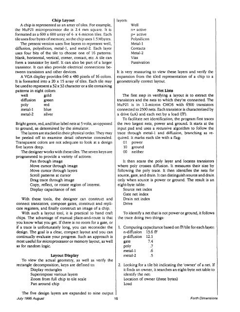
Chip Layout<br />
A chip is represented as an array of tiles. For example,<br />
the MuP21 microprocessor die is 2.4 mm square. It is<br />
formatted as a 600 x 600 array of 4- x 4-micron tiles. Each<br />
tile uses four bytes of memory, so the chip uses 1.5 Mbytes.<br />
The present version uses five layers to represent well,<br />
diffusion, polysilicon, metal-1, and metal-2. Each layer<br />
uses four bits of the tile to choose one of 16 patterns:<br />
blank, horizontal, vertical, corner, contact, etc. A tile can<br />
form a transistor by itself. It can also be part of a larger<br />
transistor. It can also provide electrical connections be-<br />
tween transistors and other devices.<br />
A VGA display provides 640 x 480 pixels of 16 colors.<br />
It is formatted into a 20 x 15 array of tiles. Each tile may<br />
be used to represent a 32 x 32 character or a tile containing<br />
patterns in eight colors:<br />
well gold<br />
diffusion green<br />
PO~Y red<br />
metal-1 blue<br />
metal-2 silver<br />
Bright green, red, and blue label nets at 5 volts, as opposed<br />
to ground, as determined by the simulator.<br />
The layers are stacked in their physical order. They may<br />
be peeled off to examine detail otherwise concealed.<br />
Transparent colors are not adequate to look at a design<br />
five layers deep.<br />
The designer works with these tiles. The seven keys are<br />
programmed to provide a variety of actions:<br />
Pan through image<br />
Move cursor through image<br />
Move cursor through layers<br />
Scroll patterns at cursor<br />
Drag trace through image<br />
Copy, reflect, or rotate region of interest.<br />
Display capacitance of net<br />
With these tools, the designer can construct and<br />
connect transistors, compose gates, construct and repli-<br />
cate registers, and finally construct an image of a chip.<br />
With such a layout tool, it is practical to hand craft<br />
chips. The advantage of manual place-and-route is that<br />
you know what you get. If there is no room for a gate, or<br />
if a trace is unfortunately long, you can reconsider the<br />
design. The goal is a clear, compact layout and you can<br />
continually evaluate your progress. Such an approach is<br />
most useful for microprocessor or memory layout, as well<br />
as for random logic.<br />
Layout Display<br />
To view the actual geometry, as well as verify the<br />
rectangle decomposition, keys are defined to:<br />
Display rectangles<br />
Superimpose various layers<br />
Zoom from full chip to tile scale<br />
Pan around chip<br />
The five design layers are expanded to nine output I<br />
July 1995 August 16<br />
layers:<br />
Well<br />
n+ active<br />
p+ active<br />
Polysilicon<br />
Metal-1<br />
Contacts<br />
Metal-2<br />
Vias<br />
Passivation<br />
It is very reassuring to view these layers and verify the<br />
expansion from the tiled representation of a chip to a<br />
geometrically correct layout.<br />
Net Lists<br />
The first step in verifying a layout is to extract the<br />
transistors and the nets to which they're connected. The<br />
MuP21 is in 1.2-micron CMOS with 6500 transistors<br />
connected to 2500 nets. Each transistor is characterized by<br />
a drive (uA) and each net by a load (P).<br />
To facilitate net identification, the program first traces<br />
the two largest nets, power and ground. It starts at the<br />
input pad and uses a recursive algorithm to follow the<br />
trace through metal-1 and diffusion, branching as re-<br />
quired. It marks each tile with a flag:<br />
01 power<br />
10 ground<br />
00 neither<br />
It then scans the poly layer and locates transistors<br />
where poly crosses diffusion. It measures their size by<br />
following the poly trace. It then identifies the nets for<br />
source, gate, and drain. It can distinguishsource and drain<br />
only when source is power or ground. The result is an<br />
eight-byte table:<br />
Source net index<br />
Gate net index<br />
Drain net index<br />
Drive<br />
To identify a net that is not power or ground, it follows<br />
the trace doing two things:<br />
1. Computing capacitance based on P/tile for each layer:<br />
n-diffusion 13.6 fF<br />
p-diffusion 12.1<br />
gate 7.4<br />
PO~Y .7<br />
metal-1 .6<br />
metal-2 .5<br />
2. Looking for a tile bit indicating the 'owner' of a net. If<br />
it finds an owner, it searches an eight-byte net table to<br />
identify the net:<br />
Location of owner (three bytes)<br />
Load<br />
I<br />
<strong>Forth</strong> Dimensions


