BUX98 BUX98A
BUX98 BUX98A
BUX98 BUX98A

Create successful ePaper yourself
Turn your PDF publications into a flip-book with our unique Google optimized e-Paper software.
<strong>BUX98</strong><br />
<strong>BUX98</strong>A<br />
HIGH POWER NPN SILICON TRANSISTORS<br />
■<br />
■<br />
■<br />
■<br />
■<br />
SGS-THOMSON PREFERRED SALESTYPES<br />
NPN TRANSISTOR<br />
HIGH VOLTAGE CAPABILITY<br />
HIGH CURRENT CAPABILITY<br />
FAST SWITCHING SPEED<br />
APPLICATIONS<br />
■ HIGH FREQUENCY AND EFFICENCY<br />
CONVERTERS<br />
■ LINEAR AND SWITCHING INDUSTRIAL<br />
EQUIPMENT<br />
1<br />
2<br />
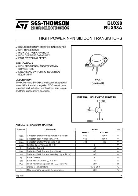
DESCRIPTION<br />
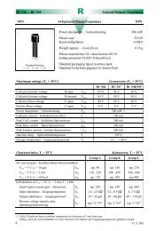
The <strong>BUX98</strong> and <strong>BUX98</strong>A are silicon multiepitaxial<br />
mesa NPN transistor in jedec TO-3 metal case,<br />
intended and industrial applications from single<br />
and three-phase mains operation.<br />
TO-3<br />
(version R)<br />
INTERNAL SCHEMATIC DIAGRAM<br />
ABSOLUTE MAXIMUM RATINGS<br />
Symbol Parameter Value Unit<br />
<strong>BUX98</strong><br />
<strong>BUX98</strong>A<br />
V CER Collector-Emitter Voltage (RBE = ≤ 10 Ω) 850 1000 V<br />
V CES Collector-Base Voltage (V BE = 0) 850 1000 V<br />
VCEO Collector-Emitter Voltage (IB = 0) 400 450 V<br />
V EBO Emitter-Base Voltage (IC = 0) 7 V<br />
I C Collector Current 30 A<br />
I CM Collector Peak Current (tp < 5 ms) 60 A<br />
I CP Collector Peak Current non Rep. (tp < 20 µs) 80 A<br />
I B Base Current 8 A<br />
IBM Base Peak Current (tp < 5 ms) 30 A<br />
Ptot Total Power Dissipation at Tcase < 25 o C 250 W<br />
T stg Storage Temperature -65 to 200<br />
T j Max Operating Junction Temperature 200<br />
o C<br />
o C<br />
July 1997<br />
1/4
<strong>BUX98</strong> / <strong>BUX98</strong>A<br />
THERMAL DATA<br />
R thj-case Thermal Resistance Junction-case Max 0.7<br />
o C/W<br />
ELECTRICAL CHARACTERISTICS (T case = 25 o C unless otherwise specified)<br />
Symbol Parameter Test Conditions Min. Typ. Max. Unit<br />
I CER<br />
I CES<br />
I CEO<br />
I EBO<br />
V CEO(sus)∗<br />
V CER(sus)∗<br />
VCE(sat)∗<br />
V BE(sat)∗<br />
Collector Cut-off<br />
Current (RBE = 10 Ω)<br />
Collector Cut-off<br />
Current (VBE = 0 )<br />
Collector Cut-off<br />
Current (I B = 0)<br />
Emitter Cut-off Current<br />
(IC = 0)<br />
Collector-Emitter<br />
Sustaining Voltage<br />
Collector-Emitter<br />
Sustaining Voltage<br />
Collector-Emitter<br />
Saturation Voltage<br />
V CE = V CES<br />
VCE = VCES<br />
V CE = V CES<br />
VCE = VCES<br />
TCASE = 125 o C<br />
TCASE = 125 o C<br />
1<br />
8<br />
400<br />
4<br />
µA<br />
mA<br />
µA<br />
mA<br />
V CE = V CEO 2 mA<br />
V EB = 5 V 2 mA<br />
I C = 200 mA<br />
for <strong>BUX98</strong><br />
for <strong>BUX98</strong>A<br />
L = 2mH<br />
for <strong>BUX98</strong><br />
for <strong>BUX98</strong>A<br />
for <strong>BUX98</strong><br />
I C = 20 A<br />
for <strong>BUX98</strong>A<br />
IC = 16 A<br />
I C = 24 A<br />
I C = 1 A<br />
I B = 4 A<br />
IB = 3.2 A<br />
I B = 5 A<br />
400<br />
450<br />
850<br />
1000<br />
Base-Emitter<br />
Saturation Voltage<br />
for <strong>BUX98</strong><br />
I C = 20 A<br />
I B = 4 A<br />
1.6 V<br />
for <strong>BUX98</strong>A<br />
I C = 16 A<br />
I B = 3.2 A<br />
1.6 V<br />
t on Turn-on Time for <strong>BUX98</strong> 1 µs<br />
ts Storage Time VCC = 150 V IC = 20 A 3 µs<br />
t f Fall Time I B1 = - I B2 = 4 A 0.8 µs<br />
t on Turn-on Time for <strong>BUX98</strong>A 1 µs<br />
t s Storage Time V CC = 150 V I C = 16 A 3 µs<br />
tf Fall Time IB1 = - IB2 = 3.2 A 0.8 µs<br />
∗ Pulsed: Pulse duration = 300 µs, duty cycle = 1.5 %<br />
1.5<br />
1.5<br />
5<br />
V<br />
V<br />
V<br />
V<br />
V<br />
V<br />
V<br />
2/4
<strong>BUX98</strong> / <strong>BUX98</strong>A<br />
TO-3 (version R) MECHANICAL DATA<br />
DIM.<br />
mm<br />
inch<br />
MIN. TYP. MAX. MIN. TYP. MAX.<br />
A 11.7 0.460<br />
B 0.96 1.10 0.037 0.043<br />
C 1.70 0.066<br />
D 8.7 0.342<br />
E 20.0 0.787<br />
G 10.9 0.429<br />
N 16.9 0.665<br />
P 26.2 1.031<br />
R 3.88 4.09 0.152 0.161<br />
U 39.50 1.555<br />
V 30.10 1.185<br />
P<br />
G<br />
A<br />
D<br />
C<br />
U<br />
V<br />
B<br />
E<br />
N<br />
O<br />
R<br />
P003N<br />
3/4
<strong>BUX98</strong> / <strong>BUX98</strong>A<br />
Information furnished is believed to be accurate and reliable. However, SGS-THOMSON Microelectronics assumes no responsability for the<br />
consequences of use of such information nor for any infringement of patents or other rights of third parties which may results from its use. No<br />
license is granted by implication or otherwise under any patent or patent rights of SGS-THOMSON Microelectronics. Specifications mentioned<br />
in this publication are subject to change without notice. This publication supersedes and replaces all information previously supplied.<br />
SGS-THOMSON Microelectronics products are not authorized for use as critical components in life support devices or systems without express<br />
written approval of SGS-THOMSON Microelectonics.<br />
© 1997 SGS-THOMSON Microelectronics - Printed in Italy - All Rights Reserved<br />
SGS-THOMSON Microelectronics GROUP OF COMPANIES<br />
Australia - Brazil - Canada - China - France - Germany - Hong Kong - Italy - Japan - Korea - Malaysia - Malta - Morocco - The Netherlands -<br />
Singapore - Spain - Sweden - Switzerland - Taiwan - Thailand - United Kingdom - U.S.A<br />
. . .<br />
4/4