Fundamental characteristics of thyristors - Educypedia
Fundamental characteristics of thyristors - Educypedia
Fundamental characteristics of thyristors - Educypedia

Create successful ePaper yourself
Turn your PDF publications into a flip-book with our unique Google optimized e-Paper software.
Teccor ® brand Thyristors<br />
AN1001<br />
<strong>Fundamental</strong> Characteristics <strong>of</strong> Thyristors<br />
Introduction<br />
The Thyristor family <strong>of</strong> semiconductors consists <strong>of</strong> several<br />
very useful devices. The most widely used <strong>of</strong> this family<br />
are silicon controlled rectifiers (SCRs), Triacs, SIDACs, and<br />
DIACs. In many applications these devices perform key<br />
functions and are real assets in meeting environmental,<br />
speed, and reliability specifications which their electromechanical<br />
counterparts cannot fulfill.<br />
This application note presents the basic fundamentals<br />
<strong>of</strong> SCR, Triac, SIDAC, and DIAC Thyristors so the user<br />
understands how they differ in <strong>characteristics</strong> and<br />
parameters from their electro-mechanical counterparts.<br />
Also, Thyristor terminology is defined.<br />
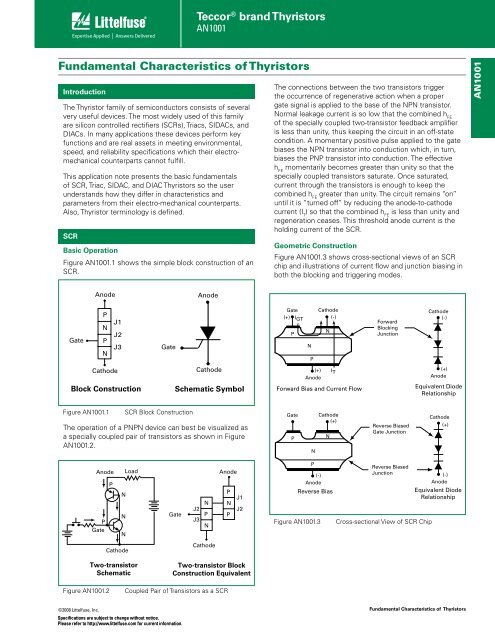
SCR<br />
Basic Operation<br />
Figure AN1001.1 shows the simple block construction <strong>of</strong> an<br />
SCR.<br />
The connections between the two transistors trigger<br />
the occurrence <strong>of</strong> regenerative action when a proper<br />
gate signal is applied to the base <strong>of</strong> the NPN transistor.<br />
Normal leakage current is so low that the combined h FE<br />
<strong>of</strong> the specially coupled two-transistor feedback amplifier<br />
is less than unity, thus keeping the circuit in an <strong>of</strong>f-state<br />
condition. A momentary positive pulse applied to the gate<br />
biases the NPN transistor into conduction which, in turn,<br />
biases the PNP transistor into conduction. The effective<br />
h FE<br />
momentarily becomes greater than unity so that the<br />
specially coupled transistors saturate. Once saturated,<br />
current through the transistors is enough to keep the<br />
combined h FE<br />
greater than unity. The circuit remains “on”<br />
until it is “turned <strong>of</strong>f” by reducing the anode-to-cathode<br />
current (I T<br />
) so that the combined h FE<br />
is less than unity and<br />
regeneration ceases. This threshold anode current is the<br />
holding current <strong>of</strong> the SCR.<br />
Geometric Construction<br />
Figure AN1001.3 shows cross-sectional views <strong>of</strong> an SCR<br />
chip and illustrations <strong>of</strong> current flow and junction biasing in<br />
both the blocking and triggering modes.<br />
AN1001<br />
Anode<br />
Anode<br />
Gate<br />
P<br />
N<br />
P<br />
N<br />
J1<br />
J2<br />
J3<br />
Gate<br />
Gate<br />
(+) I GT<br />
P<br />
N<br />
P<br />
Cathode<br />
(-)<br />
N<br />
Forward<br />
Blocking<br />
Junction<br />
Cathode<br />
(-)<br />
Cathode<br />
Block Construction<br />
Cathode<br />
Schematic Symbol<br />
(+)<br />
Anode<br />
I T<br />
Forward Bias and Current Flow<br />
(+)<br />
Anode<br />
Equivalent Diode<br />
Relationship<br />
Figure AN1001.1<br />
SCR Block Construction<br />
The operation <strong>of</strong> a PNPN device can best be visualized as<br />
a specially coupled pair <strong>of</strong> transistors as shown in Figure<br />
AN1001.2.<br />
Gate<br />
P<br />
N<br />
Cathode<br />
(+)<br />
N<br />
Reverse Biased<br />
Gate Junction<br />
Cathode<br />
(+)<br />
Anode<br />
P<br />
P<br />
Gate<br />
Load<br />
N<br />
N<br />
N<br />
Gate<br />
J2<br />
J3<br />
N<br />
P<br />
N<br />
Anode<br />
P<br />
J1<br />
N<br />
J2<br />
P<br />
P<br />
(-)<br />
Anode<br />
Reverse Bias<br />
Figure AN1001.3<br />
Reverse Biased<br />
Junction (-)<br />
Anode<br />
Equivalent Diode<br />
Relationship<br />
Cross-sectional View <strong>of</strong> SCR Chip<br />
Cathode<br />
Cathode<br />
Two-transistor<br />
Schematic<br />
Two-transistor Block<br />
Construction Equivalent<br />
Figure AN1001.2<br />
Coupled Pair <strong>of</strong> Transistors as a SCR<br />
©2008 Littelfuse, Inc.<br />
Specifications are subject to change without notice.<br />
Please refer to http://www.littelfuse.com for current information.<br />
<strong>Fundamental</strong> Characteristics <strong>of</strong> Thyristors
Teccor ® brand Thyristors<br />
AN1001<br />
Triac<br />
Basic Operation<br />
Figure AN1001.4 shows the simple block construction <strong>of</strong> a<br />
Triac. Its primary function is to control power bilaterally in<br />
an AC circuit.<br />
Geometric Construction<br />
Figure AN1001.6 show simplified cross-sectional views <strong>of</strong> a<br />
Triac chip in various gating quadrants and blocking modes.<br />
GATE(+)<br />
MT1(-)<br />
I GT<br />
N<br />
Main<br />
Terminal 2<br />
(MT2)<br />
N<br />
P N P<br />
N<br />
N<br />
Main<br />
Terminal 1<br />
(MT1)<br />
Gate<br />
P<br />
N<br />
N<br />
P<br />
N<br />
MT1(-)<br />
Block Construction<br />
MT2<br />
I T<br />
MT2(+)<br />
QUADRANT I<br />
Blocking<br />
Junction<br />
GATE(-)<br />
I GT<br />
MT1(-)<br />
Gate<br />
N<br />
P<br />
N<br />
N<br />
P<br />
N<br />
MT2(+)<br />
Equivalent Diode<br />
Relationship<br />
MT1<br />
Schematic Symbol<br />
MT2(+)<br />
QUADRANT II<br />
Figure AN1001.4<br />
Triac Block Construction<br />
Operation <strong>of</strong> a Triac can be related to two SCRs connected<br />
in parallel in opposite directions as shown in Figure<br />
AN1001.5.<br />
GATE(-)<br />
N<br />
MT1(+)<br />
N P<br />
I GT<br />
QUADRANT III<br />
N<br />
Although the gates are shown separately for each SCR,<br />
a Triac has a single gate and can be triggered by either<br />
polarity.<br />
MT1<br />
P<br />
MT2(-)<br />
N<br />
GATE(+) MT1(+)<br />
I GT<br />
N N P<br />
N<br />
P<br />
N<br />
MT2(-)<br />
I T<br />
I T<br />
QUADRANT IV<br />
Blocking<br />
Junction<br />
MT1(+)<br />
MT2(-)<br />
Equivalent Diode<br />
Relationship<br />
Figure AN1001.6<br />
Simplified Cross-sectional <strong>of</strong> Triac Chip<br />
MT2<br />
Figure AN1001.5<br />
SCRs Connected as a Triac<br />
Since a Triac operates in both directions, it behaves<br />
essentially the same in either direction as an SCR would<br />
behave in the forward direction (blocking or operating).<br />
<strong>Fundamental</strong> Characteristics <strong>of</strong> Thyristors<br />
©2008 Littelfuse, Inc.<br />
Specifications are subject to change without notice.<br />
Please refer to http://www.littelfuse.com for current information.
Teccor ® brand Thyristors<br />
AN1001<br />
SIDAC<br />
Basic Operation<br />
The SIDAC is a multi-layer silicon semiconductor switch.<br />
Figure AN1001.7 illustrates its equivalent block construction<br />
using two Shockley diodes connected inverse parallel.<br />
Figure AN1001.7 also shows the schematic symbol for the<br />
SIDAC.<br />
DIAC<br />
Basic Operation<br />
The construction <strong>of</strong> a DIAC is similar to an open base<br />
NPN transistor. Figure AN1001.9 shows a simple block<br />
construction <strong>of</strong> a DIAC and its schematic symbol.<br />
AN1001<br />
MT1<br />
MT1<br />
MT1<br />
N<br />
P<br />
N<br />
MT2<br />
MT1<br />
MT2<br />
N<br />
P<br />
N<br />
P<br />
2<br />
3<br />
4<br />
5<br />
Figure AN1001.7<br />
MT2<br />
P<br />
N<br />
P<br />
1<br />
N<br />
Equivalent Diode Relationship<br />
2<br />
3<br />
4<br />
SIDAC Block Construction<br />
MT1<br />
MT2<br />
Schematic Symbol<br />
The SIDAC operates as a bidirectional switch activated<br />
by voltage. In the <strong>of</strong>f state, the SIDAC exhibits leakage<br />
currents (I DRM<br />
) less than 5 μA. As applied voltage exceeds<br />
the SIDAC V BO<br />
, the device begins to enter a negative<br />
resistance switching mode with <strong>characteristics</strong> similar to<br />
an avalanche diode. When supplied with enough current<br />
(I S<br />
), the SIDAC switches to an on state, allowing high<br />
current to flow. When it switches to on state, the voltage<br />
across the device drops to less than 5 V, depending on<br />
magnitude <strong>of</strong> the current flow. When the SIDAC switches<br />
on and drops into regeneration, it remains on as long as<br />
holding current is less than maximum value (150 mA,<br />
typical value <strong>of</strong> 30 mA to 65 mA). The switching current (I S<br />
)<br />
is very near the holding current (I H<br />
) value. When the SIDAC<br />
switches, currents <strong>of</strong> 10 A to 100 A are easily developed by<br />
discharging small capacitor into primary or small, very highvoltage<br />
transformers for 10 μs to 20 μs.<br />
The main application for SIDACs is ignition circuits or<br />
inexpensive high voltage power supplies.<br />
Geometric Construction<br />
Block Construction<br />
Figure AN1001.9<br />
Load<br />
MT1<br />
N<br />
P<br />
N<br />
DIAC Block Construction<br />
Schematic Symbol<br />
The bidirectional transistor-like structure exhibits a highimpedance<br />
blocking state up to a voltage breakover point<br />
(V BO<br />
) above which the device enters a negative-resistance<br />
region. These basic DIAC <strong>characteristics</strong> produce a<br />
bidirectional pulsing oscillator in a resistor-capacitor AC<br />
circuit. Since the DIAC is a bidirectional device, it makes<br />
a good economical trigger for firing Triacs in phase control<br />
circuits such as light dimmers and motor speed controls.<br />
Figure AN1001.10 shows a simplified AC circuit using a<br />
DIAC and a Triac in a phase control application.<br />
Figure AN1001.10<br />
Geometric Construction<br />
AC Phase Control Circuit<br />
MT1<br />
MT2<br />
MT2<br />
P 1<br />
N 2<br />
P 3<br />
N 4<br />
Figure AN1001.11<br />
Cross-section <strong>of</strong> Chip<br />
Equivalent Diode<br />
Relationship<br />
Cross-sectional View <strong>of</strong> DIAC Chip<br />
P 5<br />
MT2<br />
Figure AN1001.8<br />
Cross-sectional View <strong>of</strong> a Bidirectional SIDAC<br />
Chip with Multi-layer Construction<br />
©2008 Littelfuse, Inc.<br />
Specifications are subject to change without notice.<br />
Please refer to http://www.littelfuse.com for current information.<br />
<strong>Fundamental</strong> Characteristics <strong>of</strong> Thyristors
Teccor ® brand Thyristors<br />
AN1001<br />
Electrical Characteristic Curves <strong>of</strong> Thyristors<br />
+I<br />
+I<br />
Voltage Drop (V T ) at<br />
Specified Current (i T )<br />
Latching Current (I L )<br />
I T<br />
I H<br />
R S<br />
Reverse Leakage<br />
Current - (I RRM ) at<br />
Specified V RRM<br />
-V<br />
Minimum Holding<br />
Current (I H )<br />
Specified Minimum<br />
Reverse Blocking<br />
Voltage (V RRM )<br />
Specified Minimum<br />
Off - State<br />
Blocking<br />
Voltage (V DRM )<br />
Off - State Leakage<br />
Current - (I DRM ) at<br />
Specified V DRM<br />
+V<br />
I S<br />
I BO<br />
I DRM<br />
-V<br />
(V BO - V S )<br />
R S =<br />
(I S - I BO )<br />
V T<br />
+V<br />
V BO<br />
V S<br />
V DRM<br />
Reverse<br />
Breakdown<br />
Voltage<br />
-I<br />
Forward<br />
Breakover<br />
Voltage<br />
-I<br />
Figure AN1001.12<br />
V-I Characteristics <strong>of</strong> SCR Device<br />
Figure AN1001.15<br />
V-I Characteristics <strong>of</strong> a SIDAC Chip<br />
-V<br />
Figure AN1001.13<br />
-V<br />
Voltage Drop (v T ) at<br />
Specified Current (i T )<br />
Minimum Holding<br />
Current (I H )<br />
10 mA<br />
Breakover<br />
Current<br />
I BO<br />
+I<br />
-I<br />
+I<br />
Specified Minimum<br />
Off-state<br />
Blocking<br />
Voltage (V DRM )<br />
Breakover<br />
Voltage<br />
Latching Current (I L )<br />
Off-state Leakage<br />
Current – (I DRM ) at<br />
Specified V DRM<br />
V-I Characteristics <strong>of</strong> Triac Device<br />
ΔV<br />
+V<br />
+V<br />
Methods <strong>of</strong> Switching on Thyristors<br />
Three general methods are available for switching<br />
Thyristors to on-state condition:<br />
<br />
<br />
<br />
Application Of Gate Signal<br />
Gate signal must exceed I GT<br />
and V GT<br />
requirements <strong>of</strong> the<br />
Thyristor used. For an SCR (unilateral device), this signal<br />
must be positive with respect to the cathode polarity. A<br />
Triac (bilateral device) can be turned on with gate signal <strong>of</strong><br />
either polarity; however, different polarities have different<br />
requirements <strong>of</strong> I GT<br />
and V GT<br />
which must be satisfied. Since<br />
DIACs and SIDACs do not have a gate, this method <strong>of</strong> turnon<br />
is not applicable. In fact, the single major application <strong>of</strong><br />
DIACs is to switch on Triacs.<br />
Static dv/dt Turn-on<br />
<br />
applied across the anode and cathode terminals <strong>of</strong> an<br />
SCR or the main terminals <strong>of</strong> a Triac. Due to the nature <strong>of</strong><br />
Thyristor construction, a small junction capacitor is formed<br />
across each PN junction. Figure AN1001.16 shows how<br />
typical internal capacitors are linked in gated Thyristors.<br />
Breakover<br />
Voltage<br />
V BO<br />
-I<br />
Figure AN1001.14<br />
V-I Characteristics <strong>of</strong> Bilateral Trigger DIAC<br />
Figure AN1001.16<br />
Internal Capacitors Linked in Gated Thyristors<br />
<strong>Fundamental</strong> Characteristics <strong>of</strong> Thyristors<br />
©2008 Littelfuse, Inc.<br />
Specifications are subject to change without notice.<br />
Please refer to http://www.littelfuse.com for current information.
Teccor ® brand Thyristors<br />
AN1001<br />
When voltage is impressed suddenly across a PN junction,<br />
a charging current flows, equal to:<br />
i = C (<br />
dv __<br />
dt )<br />
When C (<br />
dv __<br />
dt ) becomes greater or equal to Thyristor I GT<br />
,<br />
the Thyristor switches on. Normally, this type <strong>of</strong> turn-on<br />
does not damage the device, providing the surge current is<br />
limited.<br />
Generally, Thyristor application circuits are designed with<br />
<br />
anticipated.<br />
Voltage Breakover Turn-on<br />
This method is used to switch on SIDACs and DIACs.<br />
However, exceeding voltage breakover <strong>of</strong> SCRs and Triacs<br />
is definitely not recommended as a turn-on method.<br />
In the case <strong>of</strong> SCRs and Triacs, leakage current increases<br />
until it exceeds the gate current required to turn on these<br />
gated Thyristors in a small localized point. When turn-on<br />
occurs by this method, localized heating in a small area<br />
<br />
increasing current is not sufficiently limited.<br />
DIACs used in typical phase control circuits are basically<br />
protected against excessive current at breakover as long<br />
as the firing capacitor is not excessively large. When DIACs<br />
are used in a zener function, current limiting is necessary.<br />
SIDACs are typically pulse-firing, high-voltage transformers<br />
and are current limited by the transformer primary. The<br />
SIDAC should be operated so peak current amplitude,<br />
<br />
Triac Gating Modes Of Operation<br />
Triacs can be gated in four basic gating modes as shown in<br />
Figure AN1001.17.<br />
(-)<br />
I GT<br />
GATE<br />
ALL POLARITIES ARE REFERENCED TO MT1<br />
MT2 POSITIVE<br />
(Positive Half Cycle)<br />
MT2<br />
+<br />
(+) I GT<br />
GATE<br />
MT2<br />
most optimum in Quadrants I and III due to the inherent<br />
Thyristor chip construction. If Quadrants I and III cannot be<br />
used, the next best operating modes are Quadrants II and<br />
III where the gate has a negative polarity supply with an AC<br />
main terminal supply. Typically, Quadrant II is approximately<br />
equal in gate sensitivity to Quadrant I; however, latching<br />
current sensitivity in Quadrant II is lowest. Therefore, it is<br />
difficult for Triacs to latch on in Quadrant II when the main<br />
terminal current supply is very low in value.<br />
Special consideration should be given to gating circuit<br />
design when Quadrants I and IV are used in actual<br />
application, because Quadrant IV has the lowest gate<br />
sensitivity <strong>of</strong> all four operating quadrants.<br />
General Terminology<br />
The following definitions <strong>of</strong> the most widely-used Thyristor<br />
terms, symbols, and definitions conform to existing EIA-<br />
JEDEC standards:<br />
Breakover Point − Any point on the principal voltage-current<br />
characteristic for which the differential resistance is zero and<br />
where the principal voltage reaches a maximum value<br />
Principal Current − Generic term for the current through<br />
the collector junction (the current through main terminal 1<br />
and main terminal 2 <strong>of</strong> a Triac or anode and cathode <strong>of</strong> an<br />
SCR)<br />
Principal Voltage − Voltage between the main terminals:<br />
(1) In the case <strong>of</strong> reverse blocking Thyristors, the principal<br />
voltage is called positive when the anode potential is<br />
higher than the cathode potential and negative when<br />
the anode potential is lower than the cathode potential.<br />
(2) For bidirectional Thyristors, the principal voltage is called<br />
positive when the potential <strong>of</strong> main terminal 2 is higher<br />
than the potential <strong>of</strong> main terminal 1.<br />
Off State − Condition <strong>of</strong> the Thyristor corresponding to the<br />
high-resistance, low-current portion <strong>of</strong> the principal voltagecurrent<br />
characteristic between the origin and the breakover<br />
point(s) in the switching quadrant(s)<br />
AN1001<br />
I GT<br />
-<br />
REF<br />
MT2<br />
MT1<br />
QII<br />
QIII<br />
QI<br />
QIV<br />
MT1<br />
REF<br />
+ I GT<br />
MT2<br />
On State − Condition <strong>of</strong> the Thyristor corresponding to the<br />
low-resistance, low-voltage portion <strong>of</strong> the principal voltagecurrent<br />
characteristic in the switching quadrant(s).<br />
(-) I GT<br />
GATE<br />
(+) I GT<br />
GATE<br />
REF<br />
MT1<br />
-<br />
MT2 NEGATIVE<br />
(Negative Half Cycle)<br />
REF<br />
NOTE: Alternistors will not operate in Q IV<br />
MT1<br />
Figure AN1001.17<br />
Gating Modes<br />
The most common quadrants for Triac gating-on are<br />
Quadrants I and III, where the gate supply is synchronized<br />
with the main terminal supply (gate positive -- MT2 positive,<br />
gate negative -- MT2 negative). Gate sensitivity <strong>of</strong> Triacs is<br />
©2008 Littelfuse, Inc.<br />
Specifications are subject to change without notice.<br />
Please refer to http://www.littelfuse.com for current information.<br />
<strong>Fundamental</strong> Characteristics <strong>of</strong> Thyristors
Teccor ® brand Thyristors<br />
AN1001<br />
Specific Terminology<br />
Average Gate Power Dissipation [P G(AV)<br />
] − Value <strong>of</strong> gate<br />
power which may be dissipated between the gate and main<br />
terminal 1 (or cathode) averaged over a full cycle<br />
Breakover Current (I BO<br />
) − Principal current at the breakover<br />
point<br />
Breakover Voltage (V BO<br />
) − Principal voltage at the<br />
breakover point<br />
Circuit-commutated Turn-<strong>of</strong>f Time (t q<br />
) − Time interval<br />
between the instant when the principal current has<br />
decreased to zero after external switching <strong>of</strong> the principal<br />
voltage circuit and the instant when the Thyristor is capable<br />
<strong>of</strong> supporting a specified principal voltage without turning on<br />
Critical Rate-<strong>of</strong>-rise <strong>of</strong> Commutation Voltage <strong>of</strong> a Triac<br />
(Commutating dv/dt) − Minimum value <strong>of</strong> the rate-<strong>of</strong>-rise<br />
<strong>of</strong> principal voltage which will cause switching from the <strong>of</strong>f<br />
state to the on state immediately following on-state current<br />
conduction in the opposite quadrant<br />
Critical Rate-<strong>of</strong>-rise <strong>of</strong> Off-state Voltage or Static dv/<br />
dt (dv/dt) − Minimum value <strong>of</strong> the rate-<strong>of</strong>-rise <strong>of</strong> principal<br />
voltage which will cause switching from the <strong>of</strong>f state to the<br />
on state<br />
Critical Rate-<strong>of</strong>-rise <strong>of</strong> On-state Current (di/dt) −<br />
Maximum value <strong>of</strong> the rate-<strong>of</strong>-rise <strong>of</strong> on-state current that a<br />
Thyristor can withstand without harmful effect<br />
Gate-controlled Turn-on Time (t gt<br />
) − Time interval<br />
between a specified point at the beginning <strong>of</strong> the gate pulse<br />
and the instant when the principal voltage (current) has<br />
dropped to a specified low value (or risen to a specified high<br />
value) during switching <strong>of</strong> a Thyristor from <strong>of</strong>f state to the on<br />
state by a gate pulse.<br />
Gate Trigger Current (I GT<br />
) − Minimum gate current required<br />
to maintain the Thyristor in the on state<br />
Gate Trigger Voltage (V GT<br />
) − Gate voltage required to<br />
produce the gate trigger current<br />
Holding Current (I H<br />
) − Minimum principal current required<br />
to maintain the Thyristor in the on state<br />
Latching Current (I L<br />
) − Minimum principal current required<br />
to maintain the Thyristor in the on state immediately after<br />
the switching from <strong>of</strong>f state to on state has occurred and the<br />
triggering signal has been removed<br />
On-state Current (I T<br />
) − Principal current when the Thyristor<br />
is in the on state<br />
On-state Voltage (V T<br />
) − Principal voltage when the Thyristor<br />
is in the on state<br />
Peak Gate Power Dissipation (P GM<br />
) − Maximum power<br />
which may be dissipated between the gate and main<br />
terminal 1 (or cathode) for a specified time duration<br />
Repetitive Peak Off-state Current (I DRM<br />
) − Maximum<br />
instantaneous value <strong>of</strong> the <strong>of</strong>f-state current that results from<br />
the application <strong>of</strong> repetitive peak <strong>of</strong>f-state voltage<br />
Repetitive Peak Off-state Voltage (V DRM<br />
) − Maximum<br />
instantaneous value <strong>of</strong> the <strong>of</strong>f-state voltage which occurs<br />
across a Thyristor, including all repetitive transient voltages<br />
and excluding all non-repetitive transient voltages<br />
Repetitive Peak Reverse Current <strong>of</strong> an SCR (I RRM<br />
)<br />
− Maximum instantaneous value <strong>of</strong> the reverse current<br />
resulting from the application <strong>of</strong> repetitive peak reverse<br />
voltage<br />
Repetitive Peak Reverse Voltage <strong>of</strong> an SCR (V RRM<br />
)−<br />
Maximum instantaneous value <strong>of</strong> the reverse voltage which<br />
occurs across the Thyristor, including all repetitive transient<br />
voltages and excluding all non-repetitive transient voltages<br />
Surge (Non-repetitive) On-state Current (I TSM<br />
) − On-state<br />
current <strong>of</strong> short-time duration and specified waveshape<br />
Thermal Resistance, Junction to Ambient (R JA<br />
)−<br />
Temperature difference between the Thyristor junction<br />
and ambient divided by the power dissipation causing<br />
the temperature difference under conditions <strong>of</strong> thermal<br />
equilibrium<br />
Note: Ambient is the point at which temperature does not<br />
change as the result <strong>of</strong> dissipation.<br />
Thermal Resistance, Junction to Case (R JC<br />
) −<br />
Temperature difference between the Thyristor junction and<br />
the Thyristor case divided by the power dissipation causing<br />
the temperature difference under conditions <strong>of</strong> thermal<br />
equilibrium<br />
<strong>Fundamental</strong> Characteristics <strong>of</strong> Thyristors<br />
©2008 Littelfuse, Inc.<br />
Specifications are subject to change without notice.<br />
Please refer to http://www.littelfuse.com for current information.