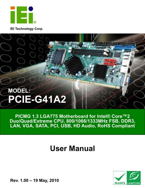
PCIE-G41A2 PICMG 1.3 CPU card - iEi
PCIE-G41A2 PICMG 1.3 CPU card - iEi
PCIE-G41A2 PICMG 1.3 CPU card - iEi

You also want an ePaper? Increase the reach of your titles
YUMPU automatically turns print PDFs into web optimized ePapers that Google loves.
<strong>PCIE</strong>-<strong>G41A2</strong> <strong>PICMG</strong> <strong>1.3</strong> <strong>CPU</strong> <strong>card</strong><br />
IEI Technology Corp.<br />
MODEL:<br />
<strong>PCIE</strong>-<strong>G41A2</strong><br />
<strong>PICMG</strong> <strong>1.3</strong> LGA775 Motherboard for Intel® Core2<br />
Duo/Quad/Extreme <strong>CPU</strong>, 800/1066/1333MHz FSB, DDR3,<br />
LAN, VGA, SATA, PCI, USB, HD Audio, RoHS Compliant<br />
User Manual<br />
Rev. 1.00 – 19 May, 2010<br />
Page i
<strong>PCIE</strong>-<strong>G41A2</strong> <strong>PICMG</strong> <strong>1.3</strong> <strong>CPU</strong> <strong>card</strong><br />
Revision<br />
Date Version Changes<br />
19 May, 2010 1.00 Initial release<br />
Page ii
<strong>PCIE</strong>-<strong>G41A2</strong> <strong>PICMG</strong> <strong>1.3</strong> <strong>CPU</strong> <strong>card</strong><br />
Copyright<br />
COPYRIGHT NOTICE<br />
The information in this document is subject to change without prior notice in order to<br />
improve reliability, design and function and does not represent a commitment on the part<br />
of the manufacturer.<br />
In no event will the manufacturer be liable for direct, indirect, special, incidental, or<br />
consequential damages arising out of the use or inability to use the product or<br />
documentation, even if advised of the possibility of such damages.<br />
This document contains proprietary information protected by copyright. All rights are<br />
reserved. No part of this manual may be reproduced by any mechanical, electronic, or<br />
other means in any form without prior written permission of the manufacturer.<br />
TRADEMARKS<br />
All registered trademarks and product names mentioned herein are used for identification<br />
purposes only and may be trademarks and/or registered trademarks of their respective<br />
owners.<br />
Page iii
<strong>PCIE</strong>-<strong>G41A2</strong> <strong>PICMG</strong> <strong>1.3</strong> <strong>CPU</strong> <strong>card</strong><br />
Table of Contents<br />
1 INTRODUCTION.......................................................................................................... 1<br />
1.1 INTRODUCTION........................................................................................................... 2<br />
1.2 BENEFITS ................................................................................................................... 2<br />
<strong>1.3</strong> FEATURES................................................................................................................... 2<br />
1.4 CONNECTORS ............................................................................................................. 3<br />
1.5 DIMENSIONS............................................................................................................... 4<br />
1.6 DATA FLOW................................................................................................................ 5<br />
1.7 TECHNICAL SPECIFICATIONS ...................................................................................... 6<br />
2 PACKING LIST............................................................................................................. 8<br />
2.1 ANTI-STATIC PRECAUTIONS........................................................................................ 9<br />
2.2 UNPACKING PRECAUTIONS......................................................................................... 9<br />
2.3 PACKING LIST........................................................................................................... 10<br />
2.4 OPTIONAL ITEMS.......................................................................................................11<br />
3 CONNECTORS ........................................................................................................... 13<br />
3.1 PERIPHERAL INTERFACE CONNECTORS..................................................................... 14<br />
3.1.1 <strong>PCIE</strong>-<strong>G41A2</strong> Layout........................................................................................ 14<br />
3.1.2 Peripheral Interface Connectors ..................................................................... 14<br />
3.<strong>1.3</strong> External Interface Panel Connectors............................................................... 15<br />
3.2 INTERNAL PERIPHERAL CONNECTORS ...................................................................... 16<br />
3.2.1 Audio Kit Connector ........................................................................................ 16<br />
3.2.2 Battery Connector............................................................................................ 17<br />
3.2.3 <strong>CPU</strong> Fan Connector ........................................................................................ 17<br />
3.2.4 <strong>CPU</strong> Power Input Connector........................................................................... 18<br />
3.2.5 Digital I/O Connector...................................................................................... 19<br />
3.2.6 Floppy Disk Connector.................................................................................... 20<br />
3.2.7 Front Panel Connector .................................................................................... 22<br />
3.2.8 Infrared Interface Connector ........................................................................... 23<br />
3.2.9 Keyboard/Mouse Connector ............................................................................ 23<br />
3.2.10 Memory Card Slot.......................................................................................... 24<br />
Page iv
<strong>PCIE</strong>-<strong>G41A2</strong> <strong>PICMG</strong> <strong>1.3</strong> <strong>CPU</strong> <strong>card</strong><br />
3.2.11 Parallel ATA (IDE) Connector....................................................................... 25<br />
3.2.12 Parallel Port Connector ................................................................................ 26<br />
3.2.13 SATA Drive Connectors ................................................................................. 27<br />
3.2.14 Serial Port Connector.................................................................................... 28<br />
3.2.15 SPI Flash Connector...................................................................................... 29<br />
3.2.16 SDVO Control Connector .............................................................................. 29<br />
3.2.17 USB Connector .............................................................................................. 30<br />
3.3 EXTERNAL PERIPHERAL INTERFACE CONNECTOR PANEL ......................................... 31<br />
3.3.1 LAN Connector ................................................................................................ 32<br />
3.3.2 USB Connector ................................................................................................ 32<br />
3.3.3 VGA Connector ................................................................................................ 33<br />
4 INSTALLATION ......................................................................................................... 34<br />
4.1 ANTI-STATIC PRECAUTIONS...................................................................................... 35<br />
4.2 INSTALLATION CONSIDERATIONS.............................................................................. 35<br />
4.2.1 Socket LGA775 <strong>CPU</strong> Installation .................................................................... 37<br />
4.2.2 Socket LGA775 Cooling Kit Installation ......................................................... 40<br />
4.2.3 DIMM Installation ........................................................................................... 42<br />
4.2.4 Backplane Installation ..................................................................................... 42<br />
4.2.5 <strong>CPU</strong> Card Installation..................................................................................... 43<br />
4.3 JUMPER SETTINGS .................................................................................................... 43<br />
4.3.1 Clear CMOS Jumper........................................................................................ 44<br />
4.4 INTERNAL PERIPHERAL DEVICE CONNECTIONS........................................................ 44<br />
4.4.1 Dual RS-232 Cable with Slot Bracket.............................................................. 44<br />
4.4.2 SATA Drive Connection ................................................................................... 45<br />
4.4.3 USB Cable (Dual Port) with Slot Bracket ....................................................... 47<br />
4.5 EXTERNAL PERIPHERAL INTERFACE CONNECTION ................................................... 48<br />
4.5.1 LAN Connection............................................................................................... 48<br />
4.5.2 USB Connection (Dual Connector) ................................................................. 49<br />
4.5.3 VGA Monitor Connection ................................................................................ 50<br />
4.6 SOFTWARE INSTALLATION ........................................................................................ 51<br />
5 BIOS.............................................................................................................................. 53<br />
5.1 INTRODUCTION......................................................................................................... 54<br />
5.1.1 Starting Setup................................................................................................... 54<br />
Page v
<strong>PCIE</strong>-<strong>G41A2</strong> <strong>PICMG</strong> <strong>1.3</strong> <strong>CPU</strong> <strong>card</strong><br />
5.1.2 Using Setup ...................................................................................................... 54<br />
5.<strong>1.3</strong> Getting Help..................................................................................................... 55<br />
5.1.4 Unable to Reboot after Configuration Changes .............................................. 55<br />
5.1.5 BIOS Menu Bar................................................................................................ 55<br />
5.2 MAIN........................................................................................................................ 56<br />
5.3 ADVANCED............................................................................................................... 57<br />
5.3.1 <strong>CPU</strong> Configuration.......................................................................................... 58<br />
5.3.2 IDE Configuration ........................................................................................... 59<br />
5.3.2.1 IDE Master, IDE Slave ............................................................................. 61<br />
5.3.3 Floppy Configuration....................................................................................... 65<br />
5.3.4 Super IO Configuration ................................................................................... 66<br />
5.3.5 Hardware Health Configuration...................................................................... 69<br />
5.3.6 Power Configuration ....................................................................................... 72<br />
5.3.6.1 ACPI Settings............................................................................................ 72<br />
5.3.6.2 APM Configuration................................................................................... 74<br />
5.3.7 Remote Access Configuration .......................................................................... 76<br />
5.3.8 USB Configuration........................................................................................... 79<br />
5.4 PCI/PNP................................................................................................................... 81<br />
5.5 BOOT........................................................................................................................ 83<br />
5.5.1 Boot Settings Configuration............................................................................. 84<br />
5.5.2 Boot Device Priority ........................................................................................ 86<br />
5.5.3 Hard Disk Drives ............................................................................................. 87<br />
5.5.4 Removable Drives ............................................................................................ 88<br />
5.5.5 CD/DVD Drives............................................................................................... 88<br />
5.6 SECURITY................................................................................................................. 89<br />
5.7 CHIPSET ................................................................................................................... 90<br />
5.7.1 Northbridge Configuration .............................................................................. 91<br />
5.7.2 Southbridge Configuration .............................................................................. 93<br />
5.8 EXIT ......................................................................................................................... 94<br />
A BIOS OPTIONS .......................................................................................................... 96<br />
B ONE KEY RECOVERY........................................................................................... 101<br />
B.1 ONE KEY RECOVERY INTRODUCTION .................................................................... 102<br />
B.1.1 System Requirement....................................................................................... 102<br />
B.1.2 Supported Operating System ......................................................................... 102<br />
Page vi
<strong>PCIE</strong>-<strong>G41A2</strong> <strong>PICMG</strong> <strong>1.3</strong> <strong>CPU</strong> <strong>card</strong><br />
B.2 SETUP PROCEDURE FOR WINDOWS........................................................................ 104<br />
B.2.1 Hardware and BIOS Setup ............................................................................ 105<br />
B.2.2 Create Partitions ........................................................................................... 105<br />
B.2.3 Install Operating System, Drivers and Applications..................................... 108<br />
B.2.4 Build-up Recovery Partition.......................................................................... 108<br />
B.2.5 Create Factory Default Image........................................................................ 111<br />
B.3 SETUP PROCEDURE FOR LINUX...............................................................................116<br />
B.4 RECOVERY TOOL FUNCTIONS .................................................................................119<br />
B.4.1 Factory Restore ............................................................................................. 121<br />
B.4.2 Backup System............................................................................................... 122<br />
B.4.3 Restore Your Last Backup.............................................................................. 123<br />
B.4.4 Manual........................................................................................................... 124<br />
C TERMINOLOGY ..................................................................................................... 125<br />
D DIGITAL I/O INTERFACE..................................................................................... 129<br />
D.1 INTRODUCTION...................................................................................................... 130<br />
D.2 DIO CONNECTOR PINOUTS ................................................................................... 130<br />
D.3 ASSEMBLY LANGUAGE EXAMPLE.......................................................................... 130<br />
E WATCHDOG TIMER............................................................................................... 131<br />
F COMPATIBILITY..................................................................................................... 134<br />
F.1 COMPATIBLE OPERATING SYSTEMS ........................................................................ 135<br />
F.2 COMPATIBLE PROCESSORS...................................................................................... 135<br />
G HAZARDOUS MATERIALS DISCLOSURE ....................................................... 136<br />
G.1 HAZARDOUS MATERIALS DISCLOSURE TABLE FOR IPB PRODUCTS CERTIFIED AS<br />
ROHS COMPLIANT UNDER 2002/95/EC WITHOUT MERCURY ..................................... 137<br />
Page vii
<strong>PCIE</strong>-<strong>G41A2</strong> <strong>PICMG</strong> <strong>1.3</strong> <strong>CPU</strong> <strong>card</strong><br />
List of Figures<br />
Figure 1-1: <strong>PCIE</strong>-<strong>G41A2</strong> .................................................................................................................2<br />
Figure 1-2: Connectors ..................................................................................................................3<br />
Figure 1-3: <strong>PCIE</strong>-<strong>G41A2</strong> Dimensions (mm)..................................................................................4<br />
Figure 1-4: Data Flow Diagram......................................................................................................5<br />
Figure 3-1: Connectors and Jumpers.........................................................................................14<br />
Figure 3-2: Audio Kit Connector Location .................................................................................16<br />
Figure 3-3: Battery Connector Location.....................................................................................17<br />
Figure 3-4: <strong>CPU</strong> Fan Connector Location ..................................................................................18<br />
Figure 3-5: <strong>CPU</strong> Power Input Connector Location....................................................................19<br />
Figure 3-6: Digital I/O Connector Locations ..............................................................................20<br />
Figure 3-7: Floppy Drive Connector Location ...........................................................................21<br />
Figure 3-8: Front Panel Connector Location .............................................................................22<br />
Figure 3-9: Infrared Connector Location....................................................................................23<br />
Figure 3-10: Keyboard/Mouse Connector Location ..................................................................24<br />
Figure 3-11: Memory Card Slot Location ...................................................................................25<br />
Figure 3-12: Parallel ATA (IDE) Connector Location ................................................................25<br />
Figure 3-13: Parallel Port Connector Location ..........................................................................27<br />
Figure 3-14: SATA Drive Connector Location ...........................................................................28<br />
Figure 3-15: Serial Port Connector Location .............................................................................28<br />
Figure 3-16: SPI Flash Connector...............................................................................................29<br />
Figure 3-17:SDVO Connector Pinout Locations........................................................................30<br />
Figure 3-18: USB Connector Pinout Locations .........................................................................31<br />
Figure 3-19: External Peripheral Interface Connector ..............................................................31<br />
Figure 3-20: VGA Connector .......................................................................................................33<br />
Figure 4-1: Intel LGA775 Socket .................................................................................................37<br />
Figure 4-2: Remove Protective Cover.........................................................................................38<br />
Figure 4-3: <strong>CPU</strong> Socket Load Plate.............................................................................................38<br />
Figure 4-4: Insert the Socket LGA775 <strong>CPU</strong>................................................................................39<br />
Figure 4-5: Cooling Kits (CF-520 and CF-775A) ........................................................................40<br />
Figure 4-6: Securing the Heat sink to the <strong>PCIE</strong>-<strong>G41A2</strong> ............................................................41<br />
Page viii
<strong>PCIE</strong>-<strong>G41A2</strong> <strong>PICMG</strong> <strong>1.3</strong> <strong>CPU</strong> <strong>card</strong><br />
Figure 4-7: DIMM Installation.......................................................................................................42<br />
Figure 4-8: Clear BIOS Jumper Location ...................................................................................44<br />
Figure 4-9: Dual RS-232 Cable Installation ................................................................................45<br />
Figure 4-10: SATA Drive Cable Connection...............................................................................46<br />
Figure 4-11: SATA Power Drive Connection..............................................................................47<br />
Figure 4-12: Dual USB Cable Connection ..................................................................................48<br />
Figure 4-13: LAN Connection ......................................................................................................49<br />
Figure 4-14: USB Connector........................................................................................................50<br />
Figure 4-15: VGA Connector .......................................................................................................51<br />
Figure 4-16: Introduction Screen ................................................................................................52<br />
Figure 4-17: Available Drivers .....................................................................................................52<br />
Figure B-1: Recovery Tool Setup Menu .................................................................................. 106<br />
Figure B-2: Command Mode..................................................................................................... 106<br />
Figure B-3: Partition Creation Commands.............................................................................. 107<br />
Figure B-4: System Configuration for Windows .................................................................... 109<br />
Figure B-5: Build-up Recovery Partition ................................................................................. 110<br />
Figure B-6: Press any key to continue .................................................................................... 110<br />
Figure B-7: Press F3 to Boot into Recovery Mode................................................................. 111<br />
Figure B-8: Recovery Tool Menu ............................................................................................. 111<br />
Figure B-9: About Symantec Ghost Window.......................................................................... 112<br />
Figure B-10: Symantec Ghost Path ......................................................................................... 112<br />
Figure B-11: Select a Local Source Drive ............................................................................... 113<br />
Figure B-12: Select a Source Partition from Basic Drive ...................................................... 113<br />
Figure B-13: File Name to Copy Image to ............................................................................... 114<br />
Figure B-14: Compress Image.................................................................................................. 114<br />
Figure B-15: Image Creation Confirmation ............................................................................. 115<br />
Figure B-16: Image Creation Complete ................................................................................... 115<br />
Figure B-17: Image Creation Complete ................................................................................... 115<br />
Figure B-18: Press Any Key to Continue ................................................................................ 116<br />
Figure B-19: Partitions for Linux.............................................................................................. 117<br />
Figure B-20: System Configuration for Linux......................................................................... 118<br />
Figure B-21: Access menu.lst in Linux (Text Mode).............................................................. 118<br />
Figure B-22: Recovery Tool Menu ........................................................................................... 119<br />
Figure B-23: Recovery Tool Main Menu .................................................................................. 120<br />
Figure B-24: Restore Factory Default...................................................................................... 121<br />
Page ix
<strong>PCIE</strong>-<strong>G41A2</strong> <strong>PICMG</strong> <strong>1.3</strong> <strong>CPU</strong> <strong>card</strong><br />
Figure B-25: Recovery Complete Window .............................................................................. 121<br />
Figure B-26: Backup System.................................................................................................... 122<br />
Figure B-27: System Backup Complete Window ................................................................... 122<br />
Figure B-28: Restore Backup ................................................................................................... 123<br />
Figure B-29: Restore System Backup Complete Window..................................................... 123<br />
Figure B-30: Symantec Ghost Window ................................................................................... 124<br />
Page x
<strong>PCIE</strong>-<strong>G41A2</strong> <strong>PICMG</strong> <strong>1.3</strong> <strong>CPU</strong> <strong>card</strong><br />
List of Tables<br />
Table 1-1: <strong>PCIE</strong>-<strong>G41A2</strong> Specifications .........................................................................................7<br />
Table 2-1: Packing List.................................................................................................................11<br />
Table 2-2: Optional Items.............................................................................................................12<br />
Table 3-1: Peripheral Interface Connectors ...............................................................................15<br />
Table 3-2: Rear Panel Connectors ..............................................................................................15<br />
Table 3-3: Audio Kit Connector Pinouts.....................................................................................16<br />
Table 3-4: Battery Connector Pinouts ........................................................................................17<br />
Table 3-5: <strong>CPU</strong> Fan Connector Pinouts......................................................................................18<br />
Table 3-6: <strong>CPU</strong> Power Input Connector Pinouts .......................................................................19<br />
Table 3-7: Digital I/O Connector Pinouts....................................................................................20<br />
Table 3-8: Floppy Drive Connector Pinouts...............................................................................21<br />
Table 3-9: Front Panel Connector Pinouts.................................................................................22<br />
Table 3-10: Infrared Connector Pinouts .....................................................................................23<br />
Table 3-11: Keyboard/Mouse Connector Pinouts .....................................................................24<br />
Table 3-12: Parallel ATA (IDE) Connector Pinouts....................................................................26<br />
Table 3-13: Parallel Port Connector Pinouts .............................................................................27<br />
Table 3-14: Serial Port Connector Pinouts ................................................................................28<br />
Table 3-15: SPI Flash Connector.................................................................................................29<br />
Table 3-16: SDVO Connector Pinouts ........................................................................................30<br />
Table 3-17: USB Port Connector Pinouts...................................................................................31<br />
Table 3-18: LAN Pinouts ..............................................................................................................32<br />
Table 3-19: USB Port Pinouts......................................................................................................32<br />
Table 3-20: VGA Connector Pinouts...........................................................................................33<br />
Table 4-1: Jumpers.......................................................................................................................44<br />
Table 4-2: Clear BIOS Jumper Settings......................................................................................44<br />
Table 5-1: BIOS Navigation Keys ................................................................................................55<br />
Page xi
<strong>PCIE</strong>-<strong>G41A2</strong> <strong>PICMG</strong> <strong>1.3</strong> <strong>CPU</strong> <strong>card</strong><br />
BIOS Menus<br />
BIOS Menu 1: Main .......................................................................................................................56<br />
BIOS Menu 2: Advanced ..............................................................................................................58<br />
BIOS Menu 3: <strong>CPU</strong> Configuration ...............................................................................................58<br />
BIOS Menu 4: IDE Configuration.................................................................................................59<br />
BIOS Menu 5: IDE Master and IDE Slave Configuration...........................................................61<br />
BIOS Menu 6: IDE Master and IDE Slave Configuration...........................................................65<br />
BIOS Menu 7: Super IO Configuration........................................................................................66<br />
BIOS Menu 8: Hardware Health Configuration ..........................................................................69<br />
BIOS Menu 9: ACPI Configuration ..............................................................................................72<br />
BIOS Menu 10: ACPI Settings .....................................................................................................73<br />
BIOS Menu 11: APM Configuration.............................................................................................74<br />
BIOS Menu 12: Remote Access Configuration..........................................................................76<br />
BIOS Menu 13: USB Configuration .............................................................................................79<br />
BIOS Menu 14: PCI/PnP Configuration.......................................................................................81<br />
BIOS Menu 15: Boot .....................................................................................................................83<br />
BIOS Menu 16: Boot Settings Configuration .............................................................................84<br />
BIOS Menu 17: Boot Device Priority Settings ...........................................................................86<br />
BIOS Menu 18: Hard Disk Drives ................................................................................................87<br />
BIOS Menu 19: Removable Drives ..............................................................................................88<br />
BIOS Menu 20: CD/DVD Drives ...................................................................................................89<br />
BIOS Menu 21: Security ...............................................................................................................89<br />
BIOS Menu 22: Chipset ................................................................................................................91<br />
BIOS Menu 23:Northbridge Chipset Configuration...................................................................91<br />
BIOS Menu 24: Southbridge Chipset Configuration .................................................................93<br />
BIOS Menu 25: Exit.......................................................................................................................94<br />
Page xii
<strong>PCIE</strong>-<strong>G41A2</strong> <strong>PICMG</strong> <strong>1.3</strong> <strong>CPU</strong> <strong>card</strong><br />
Chapter<br />
1<br />
1 Introduction<br />
Page 1
<strong>PCIE</strong>-<strong>G41A2</strong> <strong>PICMG</strong> <strong>1.3</strong> <strong>CPU</strong> <strong>card</strong><br />
1.1 Introduction<br />
Figure 1-1: <strong>PCIE</strong>-<strong>G41A2</strong><br />
The <strong>PCIE</strong>-<strong>G41A2</strong> is a PCIMG <strong>1.3</strong> motherboard with an 800/1066/1333 MHz front side bus.<br />
It accepts a Socket LGA775 Intel® Core2 Duo/Quad/Extreme processor and supports<br />
two 2.0 GB (max.) 800/1066 MHz dual-channel DDR3 DIMM modules. The <strong>PCIE</strong>-<strong>G41A2</strong><br />
includes a VGA. Expansion and I/O include support for four PCI <strong>card</strong> slots, one PCIe x16<br />
slot and one PCIe x4 slot on the backplane, High Definition audio (via audio kit), eight USB<br />
2.0 ports, four SATA connectors (RAID 0, 1, 5), FDD, IDE, parallel port interface and serial<br />
port connectors, and two Gigabit Ethernet ports.<br />
1.2 Benefits<br />
Some of the <strong>PCIE</strong>-<strong>G41A2</strong> motherboard benefits include:<br />
<strong>1.3</strong> Features<br />
• Powerful graphics<br />
• Staying connected with both wired LAN connections<br />
• Speedy running of multiple programs and applications<br />
Some of the <strong>PCIE</strong>-<strong>G41A2</strong> motherboard features are listed below:<br />
• PCIMG <strong>1.3</strong><br />
Page 2
<strong>PCIE</strong>-<strong>G41A2</strong> <strong>PICMG</strong> <strong>1.3</strong> <strong>CPU</strong> <strong>card</strong><br />
Page 3<br />
1.4 Connectors<br />
• RoHS compliant<br />
• LGA 775 <strong>CPU</strong> socket<br />
• Supports four PCI <strong>card</strong> slots, one PCIe x16 slot and one PCIe x4 slot on the<br />
backplane<br />
• Supports two dual-channel DDR3 DIMMs<br />
• Two Gigabit Ethernet connectors<br />
• Four SATA connectors<br />
• High Definition audio with optional audio kit<br />
• Intel® GMA X4500 for DX10 and OpenGL 1.5 support<br />
The connectors on the <strong>PCIE</strong>-<strong>G41A2</strong> are shown in the figure below.<br />
Figure 1-2: Connectors
<strong>PCIE</strong>-<strong>G41A2</strong> <strong>PICMG</strong> <strong>1.3</strong> <strong>CPU</strong> <strong>card</strong><br />
1.5 Dimensions<br />
The main dimensions of the <strong>PCIE</strong>-<strong>G41A2</strong> are shown in the diagram below.<br />
Figure 1-3: <strong>PCIE</strong>-<strong>G41A2</strong> Dimensions (mm)<br />
Page 4
<strong>PCIE</strong>-<strong>G41A2</strong> <strong>PICMG</strong> <strong>1.3</strong> <strong>CPU</strong> <strong>card</strong><br />
1.6 Data Flow<br />
5Figure 1-4 shows the data flow between the system chipset, the <strong>CPU</strong> and other<br />
components installed on the motherboard.<br />
Page 5<br />
Figure 1-4: Data Flow Diagram
<strong>PCIE</strong>-<strong>G41A2</strong> <strong>PICMG</strong> <strong>1.3</strong> <strong>CPU</strong> <strong>card</strong><br />
1.7 Technical Specifications<br />
<strong>PCIE</strong>-<strong>G41A2</strong> technical specifications are listed in 5Table 1-1.<br />
Specification/Model<br />
<strong>PCIE</strong>-<strong>G41A2</strong><br />
Form Factor <strong>PICMG</strong> <strong>1.3</strong><br />
<strong>CPU</strong> Supported<br />
Front Side Bus (FSB)<br />
Northbridge Chipset<br />
Integrated Graphics<br />
Socket LGA775 Intel® Core2 Duo/Quad/Extreme,<br />
Socket LGA775 Intel® Celeron®<br />
800 MHz, 1066 MHz or 1333 MHz<br />
Intel® G41<br />
350 MHz Integrated 24-bit RAMDAC<br />
Up to 2048 x 1536 32-bit color @ 75 Hz refresh<br />
Unified Memory Architecture (UMA) Uses up to 352 MB of<br />
Dynamic Video Memory Technology (DVMT)<br />
Memory<br />
Southbridge Chipset<br />
BIOS<br />
Digital I/O<br />
Ethernet Controllers<br />
Super I/O Controller<br />
Watchdog Timer<br />
Two dual-channel 2.0 GB (max.) 800 MHz or 1066 MHz<br />
DDR3 SDRAM DIMMs (system max. 4.0 GB) supported<br />
Intel® ICH7R<br />
AMI BIOS<br />
8-bit, 4-bit input/4-bit output<br />
Dual Realtek RTL8111CP<br />
iTE IT8718F<br />
Software programmable supports 1~255 sec. system reset<br />
Expansion<br />
PCI<br />
PCIe<br />
Four PCI slots via Edge Connector<br />
One PCIe x4 slot via Edge Connector<br />
One PCIe x16 slot via Edge Connector<br />
I/O Interface Connectors<br />
Audio Connectors<br />
Display port<br />
Ethernet<br />
One internal audio connector for optional audio kit<br />
One VGA<br />
Two RJ-45 ports<br />
Page 6
<strong>PCIE</strong>-<strong>G41A2</strong> <strong>PICMG</strong> <strong>1.3</strong> <strong>CPU</strong> <strong>card</strong><br />
Page 7<br />
Specification/Model<br />
Keyboard/Mouse<br />
Parallel Port<br />
Serial Ports<br />
USB 2.0/1.1 ports<br />
<strong>PCIE</strong>-<strong>G41A2</strong><br />
One PS/2 KB/MS connector<br />
One internal IEEE 1284 parallel connector (supports<br />
normal, EPP and ECP modes)<br />
Two RS-232 serial port connectors<br />
Two external USB ports<br />
Two via internal 8-pin header<br />
Four via backplane<br />
Infrared<br />
Floppy Disk Drives<br />
Parallel ATA (IDE)<br />
Serial ATA<br />
One via 5-pin header<br />
One floppy disk drive (FDD) connector<br />
One Parallel ATA (IDE) connector<br />
Four independent serial ATA (SATA) channels with<br />
3.0 Gb/s data transfer rates<br />
Environmental and Power Specifications<br />
Power Supply<br />
Power Consumption<br />
ATX supported<br />
3.3V @ 0.53A, 5V @ 6.2A, 12V @ 0.11A, Vcore_12V @<br />
2.91A (Intel® Core2 Duo E8500 3.16GHz 1333MHz<br />
FSB <strong>CPU</strong> with two 2GB DDR3 1333MHz DIMMs)<br />
Operating temperature -20ºC ~ 60ºC<br />
Humidity<br />
5% ~ 95% (non-condensing)<br />
Physical Specifications<br />
Dimensions<br />
Weight GW/NW<br />
338 mm x 126 mm<br />
1100g<br />
Table 1-1: <strong>PCIE</strong>-<strong>G41A2</strong> Specifications
<strong>PCIE</strong>-<strong>G41A2</strong> <strong>PICMG</strong> <strong>1.3</strong> <strong>CPU</strong> <strong>card</strong><br />
Chapter<br />
2<br />
2 Packing List<br />
Page 8
2.1 Anti-static Precautions<br />
WARNING!<br />
Static electricity can destroy certain electronics. Make sure to follow the<br />
ESD precautions to prevent damage to the product, and injury to the<br />
user.<br />
Make sure to adhere to the following guidelines:<br />
<strong>PCIE</strong>-<strong>G41A2</strong> <strong>PICMG</strong> <strong>1.3</strong> <strong>CPU</strong> <strong>card</strong><br />
• Wear an anti-static wristband: Wearing an anti-static wristband can prevent<br />
electrostatic discharge.<br />
• Self-grounding: Touch a grounded conductor every few minutes to discharge<br />
any excess static buildup.<br />
• Use an anti-static pad: When configuring any circuit board, place it on an<br />
anti-static mat.<br />
• Only handle the edges of the PCB: Don't touch the surface of the<br />
motherboard. Hold the motherboard by the edges when handling.<br />
2.2 Unpacking Precautions<br />
When the <strong>PCIE</strong>-<strong>G41A2</strong> is unpacked, please do the following:<br />
Page 9<br />
• Follow the antistatic guidelines above.<br />
• Make sure the packing box is facing upwards when opening.<br />
• Make sure all the packing list items are present.
<strong>PCIE</strong>-<strong>G41A2</strong> <strong>PICMG</strong> <strong>1.3</strong> <strong>CPU</strong> <strong>card</strong><br />
2.3 Packing List<br />
NOTE:<br />
If any of the components listed in the checklist below are missing, do<br />
not proceed with the installation. Contact the IEI reseller or vendor the<br />
<strong>PCIE</strong>-<strong>G41A2</strong> was purchased from or contact an IEI sales<br />
representative directly by sending an email to 32sales@iei.com.tw.<br />
The <strong>PCIE</strong>-<strong>G41A2</strong> is shipped with the following components:<br />
Quantity Item and Part Number Image<br />
1 <strong>PCIE</strong>-<strong>G41A2</strong><br />
1 Dual RS-232 cable (with bracket)<br />
(P/N: 19800-000051-RS)<br />
4 SATA cable<br />
(P/N: 32000-062800-RS)<br />
1 USB cable<br />
(P/N: CB-USB02-RS<br />
1 Mini jumper pack (2.0mm)<br />
(P/N: 33100-000033-RS)<br />
1 Utility CD<br />
Page 10
<strong>PCIE</strong>-<strong>G41A2</strong> <strong>PICMG</strong> <strong>1.3</strong> <strong>CPU</strong> <strong>card</strong><br />
Page 11<br />
Quantity Item and Part Number Image<br />
1 Quick Installation Guide<br />
Table 2-1: Packing List<br />
2.4 Optional Items<br />
The following are optional components which may be separately purchased:<br />
Item and Part Number<br />
Image<br />
<strong>CPU</strong> cooler kit<br />
(P/N: CF-520-RS-R11)<br />
<strong>CPU</strong> cooler kit<br />
(P/N: CF-775A-RS)<br />
ATA66 IDE flat cable<br />
(P/N: 32200-000052-RS)<br />
FDD cable<br />
(P/N: 32200-000017-RS)<br />
LPT cable<br />
(P/N: 19800-000049-RS)
<strong>PCIE</strong>-<strong>G41A2</strong> <strong>PICMG</strong> <strong>1.3</strong> <strong>CPU</strong> <strong>card</strong><br />
Item and Part Number<br />
Image<br />
Audio kit_ 5.1 Channel<br />
(P/N: AC-KIT08R-R10)<br />
Audio kit_ 7.1 Channel<br />
(P/N: AC-KIT-883HD-R10)<br />
PS2 cable<br />
(P/N: 19800-000075-RS)<br />
4-port USB cable<br />
(P/N: CB-USB14-RS)<br />
SATA power cable<br />
(P/N: 32102-000100-100-RS<br />
P/N: 32102-000100-200-RS)<br />
Table 2-2: Optional Items<br />
Page 12
<strong>PCIE</strong>-<strong>G41A2</strong> <strong>PICMG</strong> <strong>1.3</strong> <strong>CPU</strong> <strong>card</strong><br />
Chapter<br />
3<br />
3 Connectors<br />
Page 13
3.1 Peripheral Interface Connectors<br />
This chapter details all the jumpers and connectors.<br />
<strong>PCIE</strong>-<strong>G41A2</strong> <strong>PICMG</strong> <strong>1.3</strong> <strong>CPU</strong> <strong>card</strong><br />
3.1.1 <strong>PCIE</strong>-<strong>G41A2</strong> Layout<br />
The figure below shows all the connectors and jumpers.<br />
Figure 3-1: Connectors and Jumpers<br />
3.1.2 Peripheral Interface Connectors<br />
The table below lists all the connectors on the board.<br />
Connector Type Label<br />
Audio connector 10-pin header J_AUDIO1<br />
Battery 2-pin wafer BAT1<br />
<strong>CPU</strong> fan 4-pin wafer <strong>CPU</strong>_FAN1<br />
<strong>CPU</strong> power 4-pin connector <strong>CPU</strong>12V1<br />
DDR3 DIMM slot DIMM slot DIMM1<br />
DDR3 DIMM slot DIMM slot DIMM2<br />
Digital I/O 8-pin header DIO1<br />
FDD connector 34-pin box header FDD1<br />
Front panel 14-pin header F_PANEL1<br />
Page 14
<strong>PCIE</strong>-<strong>G41A2</strong> <strong>PICMG</strong> <strong>1.3</strong> <strong>CPU</strong> <strong>card</strong><br />
Page 15<br />
Connector Type Label<br />
Infrared interface connector 5-pin header IR1<br />
Keyboard/Mouse connector 6-pin wafer MS/KB1<br />
Parallel ATA connector (IDE) 40-pin box header PIDE1<br />
Parallel port connector 26-pin box header LPT1<br />
Serial port connector 10-pin box header COM1<br />
Serial port connector 10-pin box header COM2<br />
SATA 7-pin SATA connector SATA1<br />
SATA 7-pin SATA connector SATA2<br />
SATA 7-pin SATA connector SATA3<br />
SATA 7-pin SATA connector SATA4<br />
SPI Flash ROM 8-pin header JSPI1<br />
SVDO control connector 3-pin header J_SDVO_SM_CTRL<br />
USB 8-pin header USB1<br />
Table 3-1: Peripheral Interface Connectors<br />
3.<strong>1.3</strong> External Interface Panel Connectors<br />
The table below lists the connectors on the external I/O panel.<br />
Connector Type Label<br />
Ethernet RJ-45 LAN1<br />
Ethernet RJ-45 LAN2<br />
USB USB port USB_C1<br />
USB USB port USB_C2<br />
VGA 15-pin female VGA1<br />
Table 3-2: Rear Panel Connectors
<strong>PCIE</strong>-<strong>G41A2</strong> <strong>PICMG</strong> <strong>1.3</strong> <strong>CPU</strong> <strong>card</strong><br />
3.2 Internal Peripheral Connectors<br />
The section describes all of the connectors on the <strong>PCIE</strong>-<strong>G41A2</strong>.<br />
3.2.1 Audio Kit Connector<br />
CN Label:<br />
CN Type:<br />
J_AUDIO1<br />
9-pin header<br />
CN Location: See Figure 3-2<br />
CN Pinouts: See Table 3-3<br />
This connector connects to an external audio kit.<br />
Figure 3-2: Audio Kit Connector Location<br />
Pin Description Pin Description<br />
1 SYNC 2 BITCLK<br />
3 SDOUT 4 PCBEEP<br />
5 SDIN 6 RST#<br />
7 VCC 8 GND<br />
9 +12 V<br />
Table 3-3: Audio Kit Connector Pinouts<br />
Page 16
<strong>PCIE</strong>-<strong>G41A2</strong> <strong>PICMG</strong> <strong>1.3</strong> <strong>CPU</strong> <strong>card</strong><br />
Page 17<br />
3.2.2 Battery Connector<br />
CN Label:<br />
CN Type:<br />
BAT1<br />
2-pin wafer<br />
CN Location: See Figure 3-3<br />
CN Pinouts: See Table 3-4<br />
This is connected to the system battery. The battery provides power to the system clock to<br />
retain the time when power is turned off.<br />
Figure 3-3: Battery Connector Location<br />
Pin<br />
Description<br />
1 Battery+<br />
2 Ground<br />
Table 3-4: Battery Connector Pinouts<br />
3.2.3 <strong>CPU</strong> Fan Connector<br />
CN Label:<br />
CN Type:<br />
<strong>CPU</strong>_FAN1<br />
4-pin header<br />
CN Location: See Figure 3-4<br />
CN Pinouts: See Table 3-5<br />
The fan connector attaches to a <strong>CPU</strong> cooling fan.
<strong>PCIE</strong>-<strong>G41A2</strong> <strong>PICMG</strong> <strong>1.3</strong> <strong>CPU</strong> <strong>card</strong><br />
Figure 3-4: <strong>CPU</strong> Fan Connector Location<br />
PIN NO.<br />
DESCRIPTION<br />
1 GND<br />
2 +12 V<br />
3 Rotation Signal<br />
4 Control<br />
Table 3-5: <strong>CPU</strong> Fan Connector Pinouts<br />
3.2.4 <strong>CPU</strong> Power Input Connector<br />
CN Label:<br />
CN Type:<br />
<strong>CPU</strong>12V1<br />
4-pin connector<br />
CN Location: See Figure 3-5<br />
CN Pinouts: See Table 3-6<br />
The <strong>CPU</strong> power input connector provides power to the <strong>CPU</strong>.<br />
Page 18
<strong>PCIE</strong>-<strong>G41A2</strong> <strong>PICMG</strong> <strong>1.3</strong> <strong>CPU</strong> <strong>card</strong><br />
Page 19<br />
Figure 3-5: <strong>CPU</strong> Power Input Connector Location<br />
PIN NO.<br />
DESCRIPTION<br />
1 GND<br />
2 GND<br />
3 +12 V<br />
4 +12 V<br />
Table 3-6: <strong>CPU</strong> Power Input Connector Pinouts<br />
3.2.5 Digital I/O Connector<br />
CN Label:<br />
CN Type:<br />
DIO1<br />
10-pin header<br />
CN Location: See Figure 3-6<br />
CN Pinouts: See Table 3-7<br />
The digital I/O connector provides programmable input and output for external devices.<br />
The digital I/O provides 4-bit output and 4-bit input.
<strong>PCIE</strong>-<strong>G41A2</strong> <strong>PICMG</strong> <strong>1.3</strong> <strong>CPU</strong> <strong>card</strong><br />
Figure 3-6: Digital I/O Connector Locations<br />
PIN NO. DESCRIPTION PIN NO. DESCRIPTION<br />
1 GND 2 5 V<br />
3 Output 3 4 Output 2<br />
5 Output 1 6 Output 0<br />
7 Input 3 8 Input 2<br />
9 Input 1 10 Input 0<br />
Table 3-7: Digital I/O Connector Pinouts<br />
3.2.6 Floppy Disk Connector<br />
CN Label:<br />
CN Type:<br />
FDD1<br />
34-pin box header<br />
CN Location: See Figure 3-7<br />
CN Pinouts: See Table 3-8<br />
The floppy disk connector is connected to a floppy disk drive.<br />
Page 20
<strong>PCIE</strong>-<strong>G41A2</strong> <strong>PICMG</strong> <strong>1.3</strong> <strong>CPU</strong> <strong>card</strong><br />
Page 21<br />
Figure 3-7: Floppy Drive Connector Location<br />
Pin Description Pin Description<br />
1 GND 2 REDUCE WRITE<br />
3 GND 4 N/C<br />
5 N/C 6 N/C<br />
7 GND 8 INDEX#<br />
9 GND 10 MOTOR ENABLE A#<br />
11 GND 12 DRIVE SELECT B#<br />
13 GND 14 DRIVE SELECT A#<br />
15 GND 16 MOTOR ENABLE B#<br />
17 GND 18 DIRECTION#<br />
19 GND 20 STEP#<br />
21 GND 22 WRITE DATA#<br />
23 GND 24 WRITE GATE#<br />
25 GND 26 TRACK 0#<br />
27 GND 28 WRITE PROTECT#<br />
29 GND 30 READ DATA#<br />
31 GND 32 SIDE 1 SELECT#<br />
33 GND 34 DISK CHANGE#<br />
Table 3-8: Floppy Drive Connector Pinouts
<strong>PCIE</strong>-<strong>G41A2</strong> <strong>PICMG</strong> <strong>1.3</strong> <strong>CPU</strong> <strong>card</strong><br />
3.2.7 Front Panel Connector<br />
CN Label:<br />
CN Type:<br />
F_PANEL1<br />
14-pin header<br />
CN Location: See Figure 3-8<br />
CN Pinouts: See Table 3-9<br />
The front panel connector connects to the indicator LEDs and buttons on the computer's<br />
front panel.<br />
Figure 3-8: Front Panel Connector Location<br />
FUNCTION PIN DESCRIPTION FUNCTION PIN DESCRIPTION<br />
Power LED 1 +5 V Speaker 2 +5 V<br />
3 N/C 4 N/C<br />
5 Ground 6 N/C<br />
Power Button 7 PWRBTN- 8 Speaker<br />
9 GND Reset 10 N/C<br />
HDD LED 11 +5 V 12 Reset-<br />
13 HDD LED- 14 GND<br />
Table 3-9: Front Panel Connector Pinouts<br />
Page 22
<strong>PCIE</strong>-<strong>G41A2</strong> <strong>PICMG</strong> <strong>1.3</strong> <strong>CPU</strong> <strong>card</strong><br />
Page 23<br />
3.2.8 Infrared Interface Connector<br />
CN Label:<br />
CN Type:<br />
IR1<br />
5-pin header<br />
CN Location: See Figure 3-9<br />
CN Pinouts: See Table 3-10<br />
The infrared connector attaches to an infrared receiver for use with remote controls.<br />
Figure 3-9: Infrared Connector Location<br />
Pin<br />
Description<br />
1 VCC<br />
2 NC<br />
3 IR-RX<br />
4 GND<br />
5 IR-TX<br />
Table 3-10: Infrared Connector Pinouts<br />
3.2.9 Keyboard/Mouse Connector<br />
CN Label:<br />
CN Type:<br />
MS/KB1<br />
6-pin header<br />
CN Location: See Figure 3-10<br />
CN Pinouts: See Table 3-11
<strong>PCIE</strong>-<strong>G41A2</strong> <strong>PICMG</strong> <strong>1.3</strong> <strong>CPU</strong> <strong>card</strong><br />
The keyboard/mouse connector connects to a PS/2 Y-cable that can be connected to a<br />
PS/2 keyboard and mouse.<br />
Figure 3-10: Keyboard/Mouse Connector Location<br />
Pin<br />
Description<br />
1 +5 V<br />
2 Mouse Data<br />
3 Mouse Clock<br />
4 Keyboard Data<br />
5 Keyboard Clock<br />
6 Ground<br />
Table 3-11: Keyboard/Mouse Connector Pinouts<br />
3.2.10 Memory Card Slot<br />
CN Label:<br />
CN Type:<br />
DIMM1 and DIMM2<br />
DIMM slot<br />
CN Location: See Figure 3-11<br />
The DIMM slots are for DIMM memory modules.<br />
Page 24
<strong>PCIE</strong>-<strong>G41A2</strong> <strong>PICMG</strong> <strong>1.3</strong> <strong>CPU</strong> <strong>card</strong><br />
Page 25<br />
Figure 3-11: Memory Card Slot Location<br />
3.2.11 Parallel ATA (IDE) Connector<br />
CN Label:<br />
CN Type:<br />
IDE1<br />
40-pin box header<br />
CN Location: See Figure 3-12<br />
CN Pinouts: See Table 3-12<br />
The Parallel ATA (IDE) connector can connect to a Parallel ATA (IDE) hard drive or optical<br />
device.<br />
Figure 3-12: Parallel ATA (IDE) Connector Location
<strong>PCIE</strong>-<strong>G41A2</strong> <strong>PICMG</strong> <strong>1.3</strong> <strong>CPU</strong> <strong>card</strong><br />
Pin Description Pin Description<br />
1 RESET# 2 GND<br />
3 DATA 7 4 DATA 8<br />
5 DATA 6 6 DATA 9<br />
7 DATA 5 8 DATA 10<br />
9 DATA 4 10 DATA 11<br />
11 DATA 3 12 DATA 12<br />
13 DATA 2 14 DATA 13<br />
15 DATA 1 16 DATA 14<br />
17 DATA 0 18 DATA 15<br />
19 GND 20 N/C<br />
21 IDE DRQ 22 GND<br />
23 IOW# 24 GND<br />
25 IOR# 26 GND<br />
27 IDE CHRDY 28 BALE – DEFAULT<br />
29 IDE DACK 30 GND<br />
31 INTERRUPT 32 N/C<br />
33 SA1 34 PDIAG#<br />
35 SA0 36 SA2<br />
37 HDC CS0# 38 HDC CS1#<br />
39 HDD ACTIVE# 40 GND<br />
Table 3-12: Parallel ATA (IDE) Connector Pinouts<br />
3.2.12 Parallel Port Connector<br />
CN Label:<br />
CN Type:<br />
LPT1<br />
26-pin box header<br />
CN Location: See Figure 3-13<br />
CN Pinouts: See Table 3-13<br />
The parallel port connector connects to a parallel port connector interface or some other<br />
parallel port device such as a printer.<br />
Page 26
<strong>PCIE</strong>-<strong>G41A2</strong> <strong>PICMG</strong> <strong>1.3</strong> <strong>CPU</strong> <strong>card</strong><br />
Page 27<br />
Figure 3-13: Parallel Port Connector Location<br />
Pin Description Pin Description<br />
1 STROBE# 2 DATA 0<br />
3 DATA 1 4 DATA 2<br />
5 DATA 3 6 DATA 4<br />
7 DATA 5 8 DATA 6<br />
9 DATA 7 10 ACKNOWLEDGE<br />
11 BUSY 12 PAPER EMPTY<br />
13 PRINTER SELECT 14 AUTO FORM FEED #<br />
15 ERROR# 16 INITIALIZE<br />
17 PRINTER SELECT LN# 18 GROUND<br />
19 GROUND 20 GROUND<br />
21 GROUND 22 GROUND<br />
23 GROUND 24 GROUND<br />
25 GROUND 26 NC<br />
Table 3-13: Parallel Port Connector Pinouts<br />
3.2.13 SATA Drive Connectors<br />
CN Label:<br />
CN Type:<br />
SATA1, SATA2, SATA3, SATA4<br />
7-pin SATA drive connectors<br />
CN Location: See Figure 3-14
<strong>PCIE</strong>-<strong>G41A2</strong> <strong>PICMG</strong> <strong>1.3</strong> <strong>CPU</strong> <strong>card</strong><br />
The SATA drive connectors can be connected to SATA drives.<br />
Figure 3-14: SATA Drive Connector Location<br />
3.2.14 Serial Port Connector<br />
CN Label:<br />
CN Type:<br />
COM1, COM2<br />
10-pin header (2x5)<br />
CN Location: See Figure 3-15<br />
CN Pinouts: See Table 3-14<br />
This connector provides RS-232 communications.<br />
Figure 3-15: Serial Port Connector Location<br />
PIN NO. DESCRIPTION PIN NO. DESCRIPTION<br />
1 Data Carrier Direct (DCD) 2 Data Set Ready (DSR)<br />
3 Receive Data (RXD) 4 Request To Send (RTS)<br />
5 Transmit Data (TXD) 6 Clear To Send (CTS)<br />
7 Data Terminal Ready (DTR) 8 Ring Indicator (RI)<br />
9 Ground (GND) 10 NC<br />
Table 3-14: Serial Port Connector Pinouts<br />
Page 28
<strong>PCIE</strong>-<strong>G41A2</strong> <strong>PICMG</strong> <strong>1.3</strong> <strong>CPU</strong> <strong>card</strong><br />
Page 29<br />
3.2.15 SPI Flash Connector<br />
CN Label:<br />
CN Type:<br />
JSPI1<br />
8-pin header (2x4)<br />
CN Location: See Figure 3-16<br />
CN Pinouts: See Table 3-15<br />
The 8-pin SPI Flash connector is used to flash the BIOS.<br />
Figure 3-16: SPI Flash Connector<br />
PIN DESCRIPTION PIN DESCRIPTION<br />
1 VCC 2 GND<br />
3 CS# 4 CLOCK<br />
5 SO 6 SI<br />
7 NC 8 NC<br />
Table 3-15: SPI Flash Connector<br />
3.2.16 SDVO Control Connector<br />
CN Label:<br />
CN Type:<br />
J_SDVO_SM_CTRL<br />
3-pin header (1x3)<br />
CN Location: See Figure 3-17<br />
CN Pinouts: See Table 3-16
<strong>PCIE</strong>-<strong>G41A2</strong> <strong>PICMG</strong> <strong>1.3</strong> <strong>CPU</strong> <strong>card</strong><br />
If an SDVO graphics <strong>card</strong> is installed on the PCIe x16 expansion slot on the backplane,<br />
the 1x3 pin Serial Digital Video Output (SDVO) control connector must be connected to a<br />
corresponding SDVO control connector on a compatible IEI backplane.<br />
Figure 3-17:SDVO Connector Pinout Locations<br />
PIN NO. DESCRIPTION<br />
1 EXP_EN<br />
2 SDVO_CLOCK<br />
3 SDVO_DATA<br />
Table 3-16: SDVO Connector Pinouts<br />
3.2.17 USB Connector<br />
CN Label:<br />
CN Type:<br />
USB1<br />
8-pin header<br />
CN Location: See Figure 3-18<br />
CN Pinouts: See Table 3-17<br />
The USB connectors connect to USB devices. Each pin header provides two USB ports.<br />
Page 30
<strong>PCIE</strong>-<strong>G41A2</strong> <strong>PICMG</strong> <strong>1.3</strong> <strong>CPU</strong> <strong>card</strong><br />
Page 31<br />
Figure 3-18: USB Connector Pinout Locations<br />
PIN NO. DESCRIPTION PIN NO. DESCRIPTION<br />
1 VCC 2 GND<br />
3 DATA- 4 DATA+<br />
5 DATA+ 6 DATA-<br />
7 GND 8 VCC<br />
Table 3-17: USB Port Connector Pinouts<br />
3.3 External Peripheral Interface Connector Panel<br />
The figure below shows the external peripheral interface connector (EPIC) panel. The<br />
EPIC panel consists of the following:<br />
Figure 3-19: External Peripheral Interface Connector
<strong>PCIE</strong>-<strong>G41A2</strong> <strong>PICMG</strong> <strong>1.3</strong> <strong>CPU</strong> <strong>card</strong><br />
3.3.1 LAN Connector<br />
CN Label:<br />
CN Type:<br />
LAN1, LAN2<br />
RJ-45<br />
CN Location: See Figure 3-19<br />
CN Pinouts: See Table 3-18<br />
The LAN connector connects to a local network.<br />
PIN DESCRIPTION PIN DESCRIPTION<br />
1 MDIA3- 5 MDIA1+<br />
2 MDIA3+ 6 MDIA2+-<br />
3. MDIA2- 7 MDIA0-<br />
4. MDIA1- 8 MDIA0+<br />
Table 3-18: LAN Pinouts<br />
3.3.2 USB Connector<br />
CN Label:<br />
CN Type:<br />
USB_C1, USB_C2<br />
USB port<br />
CN Location: See Figure 3-19<br />
CN Pinouts: See Table 3-19<br />
The USB connector can be connected to a USB device.<br />
PIN NO.<br />
DESCRIPTION<br />
1 5 V<br />
2 DATA-<br />
3 DATA+<br />
4 GND<br />
Table 3-19: USB Port Pinouts<br />
Page 32
<strong>PCIE</strong>-<strong>G41A2</strong> <strong>PICMG</strong> <strong>1.3</strong> <strong>CPU</strong> <strong>card</strong><br />
Page 33<br />
3.3.3 VGA Connector<br />
CN Label:<br />
CN Type:<br />
VGA1<br />
15-pin Female<br />
CN Location: See Figure 3-19<br />
CN Pinouts: See Figure 3-20 and Table 3-20<br />
The VGA connector connects to a monitor that accepts a standard VGA input.<br />
Figure 3-20: VGA Connector<br />
PIN DESCRIPTION PIN DESCRIPTION<br />
1 RED 2 GREEN<br />
3 BLUE 4 NC<br />
5 GND 6 GND<br />
7 GND 8 GND<br />
9 VCC / NC 10 GND<br />
11 NC 12 DDC DAT<br />
13 HSYNC 14 VSYNC<br />
15 DDCCLK<br />
Table 3-20: VGA Connector Pinouts
<strong>PCIE</strong>-<strong>G41A2</strong> <strong>PICMG</strong> <strong>1.3</strong> <strong>CPU</strong> <strong>card</strong><br />
Chapter<br />
4<br />
4 Installation<br />
Page 34
4.1 Anti-static Precautions<br />
WARNING:<br />
Failure to take ESD precautions during the installation of the<br />
<strong>PCIE</strong>-<strong>G41A2</strong> may result in permanent damage to the <strong>PCIE</strong>-<strong>G41A2</strong> and<br />
severe injury to the user.<br />
Electrostatic discharge (ESD) can cause serious damage to electronic components,<br />
including the <strong>PCIE</strong>-<strong>G41A2</strong>. Dry climates are especially susceptible to ESD. It is therefore<br />
critical that whenever the <strong>PCIE</strong>-<strong>G41A2</strong> or any other electrical component is handled, the<br />
following anti-static precautions are strictly adhered to.<br />
<strong>PCIE</strong>-<strong>G41A2</strong> <strong>PICMG</strong> <strong>1.3</strong> <strong>CPU</strong> <strong>card</strong><br />
• Wear an anti-static wristband: Wearing a simple anti-static wristband can<br />
help to prevent ESD from damaging the board.<br />
• Self-grounding: Before handling the board, touch any grounded conducting<br />
material. During the time the board is handled, frequently touch any<br />
conducting materials that are connected to the ground.<br />
• Use an anti-static pad: When configuring the <strong>PCIE</strong>-<strong>G41A2</strong>, place it on an<br />
antic-static pad. This reduces the possibility of ESD damaging the<br />
<strong>PCIE</strong>-<strong>G41A2</strong>.<br />
• Only handle the edges of the PCB: When handling the PCB, hold the PCB<br />
by the edges.<br />
Page 35<br />
4.2 Installation Considerations<br />
NOTE:<br />
The following installation notices and installation considerations should<br />
be read and understood before installation. All installation notices must<br />
be strictly adhered to. Failing to adhere to these precautions may lead<br />
to severe damage and injury to the person performing the installation.
<strong>PCIE</strong>-<strong>G41A2</strong> <strong>PICMG</strong> <strong>1.3</strong> <strong>CPU</strong> <strong>card</strong><br />
WARNING:<br />
The installation instructions described in this manual should be<br />
carefully followed in order to prevent damage to the components and<br />
injury to the user.<br />
Before and during the installation please DO the following:<br />
• Read the user manual:<br />
o The user manual provides a complete description of the <strong>PCIE</strong>-<strong>G41A2</strong><br />
installation instructions and configuration options.<br />
• Wear an electrostatic discharge cuff (ESD):<br />
o Electronic components are easily damaged by ESD. Wearing an ESD cuff<br />
removes ESD from the body and helps prevent ESD damage.<br />
• Place the <strong>PCIE</strong>-<strong>G41A2</strong> on an antistatic pad:<br />
o When installing or configuring the motherboard, place it on an antistatic<br />
pad. This helps to prevent potential ESD damage.<br />
• Turn all power to the <strong>PCIE</strong>-<strong>G41A2</strong> off:<br />
o When working with the <strong>PCIE</strong>-<strong>G41A2</strong>, make sure that it is disconnected<br />
from all power supplies and that no electricity is being fed into the system.<br />
Before and during the installation of the <strong>PCIE</strong>-<strong>G41A2</strong> DO NOT:<br />
• Remove any of the stickers on the PCB board. These stickers are required for<br />
warranty validation.<br />
• Use the product before verifying all the cables and power connectors are<br />
properly connected.<br />
• Allow screws to come in contact with the PCB circuit, connector pins, or its<br />
components.<br />
Page 36
<strong>PCIE</strong>-<strong>G41A2</strong> <strong>PICMG</strong> <strong>1.3</strong> <strong>CPU</strong> <strong>card</strong><br />
Page 37<br />
4.2.1 Socket LGA775 <strong>CPU</strong> Installation<br />
NOTE:<br />
To enable Hyper-Threading, the <strong>CPU</strong> and chipset must both support it.<br />
WARNING:<br />
<strong>CPU</strong>s are expensive and sensitive components. When installing the<br />
<strong>CPU</strong> please be careful not to damage it in anyway. Make sure the <strong>CPU</strong><br />
is installed properly and ensure the correct cooling kit is properly<br />
installed.<br />
The LGA775 socket is shown in Figure 4-1.<br />
Figure 4-1: Intel LGA775 Socket<br />
To install the <strong>CPU</strong>, follow the steps below.<br />
WARNING:<br />
DO NOT touch the pins at the bottom of the <strong>CPU</strong>. When handling the<br />
<strong>CPU</strong>, only hold it on the sides.
<strong>PCIE</strong>-<strong>G41A2</strong> <strong>PICMG</strong> <strong>1.3</strong> <strong>CPU</strong> <strong>card</strong><br />
Step 1: Remove the protective cover. The black protective cover can be removed by<br />
pulling up on the tab labeled "Remove". See Figure 4-2.<br />
Figure 4-2: Remove Protective Cover<br />
Step 2: Open the socket. Disengage the load lever by pressing the lever down and<br />
slightly outward to clear the retention tab. Fully open the lever, then open the<br />
load plate. See Figure 4-3.<br />
Figure 4-3: <strong>CPU</strong> Socket Load Plate<br />
Step 3: Inspect the <strong>CPU</strong> socket. Make sure there are no bent pins and make sure the<br />
socket contacts are free of foreign material. If any debris is found, remove it with<br />
compressed air.<br />
Page 38
<strong>PCIE</strong>-<strong>G41A2</strong> <strong>PICMG</strong> <strong>1.3</strong> <strong>CPU</strong> <strong>card</strong><br />
Page 39<br />
Step 4: Orientate the <strong>CPU</strong> properly. The contact array should be facing the <strong>CPU</strong><br />
socket.<br />
Step 5: Correctly position the <strong>CPU</strong>. Match the Pin 1 mark with the cut edge on the<br />
<strong>CPU</strong> socket.<br />
Step 6: Align the <strong>CPU</strong> pins. Locate pin 1 and the two orientation notches on the <strong>CPU</strong>.<br />
Carefully match the two orientation notches on the <strong>CPU</strong> with the socket<br />
alignment keys.<br />
Step 7: Insert the <strong>CPU</strong>. Gently insert the <strong>CPU</strong> into the socket. If the <strong>CPU</strong> pins are<br />
properly aligned, the <strong>CPU</strong> should slide into the <strong>CPU</strong> socket smoothly. See<br />
Figure 4-4.<br />
Figure 4-4: Insert the Socket LGA775 <strong>CPU</strong><br />
Step 8: Close the <strong>CPU</strong> socket. Close the load plate and engage the load lever by<br />
pushing it back to its original position. There will be some resistance, but will not<br />
require extreme pressure.<br />
Step 9: Connect the 12 V power to the board. Connect the 12 V power from the power<br />
supply to the board. Step 0:
<strong>PCIE</strong>-<strong>G41A2</strong> <strong>PICMG</strong> <strong>1.3</strong> <strong>CPU</strong> <strong>card</strong><br />
4.2.2 Socket LGA775 Cooling Kit Installation<br />
WARNING:<br />
DO NOT use the original Intel® heat sink and fan. A proprietary one is<br />
recommended.<br />
Figure 4-5: Cooling Kits (CF-520 and CF-775A)<br />
The cooling kit can be bought from IEI. The cooling kit has a heatsink and fan.<br />
WARNING:<br />
Do not wipe off (accidentally or otherwise) the pre-sprayed layer of<br />
thermal paste on the bottom of the heat sink. The thermal paste<br />
between the <strong>CPU</strong> and the heat sink is important for optimum heat<br />
dissipation.<br />
To install the cooling kit, follow the instructions below.<br />
Step 1: Place the cooling kit onto the socket LGA775 <strong>CPU</strong>. Make sure the <strong>CPU</strong><br />
cable can be properly routed when the cooling kit is installed.<br />
Step 2: Properly align the cooling kit. Make sure the four spring screw fasteners can<br />
pass through the pre-drilled holes on the PCB.<br />
Page 40
<strong>PCIE</strong>-<strong>G41A2</strong> <strong>PICMG</strong> <strong>1.3</strong> <strong>CPU</strong> <strong>card</strong><br />
Page 41<br />
Step 3: Mount the cooling kit. Gently place the cooling kit on top of the <strong>CPU</strong>. Make<br />
sure the four threaded screws on the corners of the cooling kit properly pass<br />
through the predrilled holes on the bottom of the PCB.<br />
Step 4: Secure the cooling kit. From the solder side of the PCB, align the support<br />
bracket to the screw threads on heat sink that were inserted through the PCB<br />
holes. (See Figure 4-6)<br />
Figure 4-6: Securing the Heat sink to the <strong>PCIE</strong>-<strong>G41A2</strong><br />
Step 5: Tighten the screws. Use a screwdriver to tighten the four screws. Tighten each<br />
nut a few turns at a time and do not over-tighten the screws.<br />
Step 6: Connect the fan cable. Connect the cooling kit fan cable to the fan connector<br />
on the <strong>PCIE</strong>-<strong>G41A2</strong>. Carefully route the cable and avoid heat generating chips<br />
and fan blades. Step 0:
<strong>PCIE</strong>-<strong>G41A2</strong> <strong>PICMG</strong> <strong>1.3</strong> <strong>CPU</strong> <strong>card</strong><br />
4.2.3 DIMM Installation<br />
To install a DIMM, please follow the steps below and refer to Figure 4-7.<br />
Figure 4-7: DIMM Installation<br />
Step 1: Open the DIMM socket handles. Open the two handles outwards as far as<br />
they can. See Figure 4-7.<br />
Step 2: Align the DIMM with the socket. Align the DIMM so the notch on the memory<br />
lines up with the notch on the memory socket. See Figure 4-7.<br />
Step 3: Insert the DIMM. Once aligned, press down until the DIMM is properly seated.<br />
Clip the two handles into place. See Figure 4-7.<br />
Step 4: Removing a DIMM. To remove a DIMM, push both handles outward. The<br />
memory module is ejected by a mechanism in the socket.Step 0:<br />
4.2.4 Backplane Installation<br />
Before the <strong>PCIE</strong>-<strong>G41A2</strong> can be installed into the chassis, a backplane must first be<br />
installed. Please refer to the installation instructions that came with the backplane and the<br />
chassis to see how to install the backplane into the chassis.<br />
Page 42
<strong>PCIE</strong>-<strong>G41A2</strong> <strong>PICMG</strong> <strong>1.3</strong> <strong>CPU</strong> <strong>card</strong><br />
Page 43<br />
NOTE:<br />
IEI has a wide range of backplanes available. Please contact your<br />
<strong>PCIE</strong>-<strong>G41A2</strong> vendor, reseller or and IEI sales representative at<br />
sales@iei.com.tw or visit the IEI website at http://www.ieiworld.com to<br />
find out more about the available chassis.<br />
4.2.5 <strong>CPU</strong> Card Installation<br />
To install the <strong>PCIE</strong>-<strong>G41A2</strong> <strong>CPU</strong> <strong>card</strong> onto the backplane, carefully align the <strong>CPU</strong> <strong>card</strong><br />
interface connectors with the corresponding socket on the backplane. To do this, please<br />
refer to the reference material that came with the backplane. Next, secure the <strong>CPU</strong> <strong>card</strong> to<br />
the chassis. To do this, please refer to the reference material that came with the chassis.<br />
4.3 Jumper Settings<br />
NOTE:<br />
A jumper is a metal bridge used to close<br />
an electrical circuit. It consists of two or<br />
three metal pins and a small metal clip<br />
(often protected by a plastic cover) that<br />
slides over the pins to connect them. To<br />
CLOSE/SHORT a jumper means<br />
connecting the pins of the jumper with<br />
the plastic clip and to OPEN a jumper means removing the plastic clip<br />
from a jumper.<br />
The <strong>PCIE</strong>-<strong>G41A2</strong> includes one jumper shown in Table 4-1.
<strong>PCIE</strong>-<strong>G41A2</strong> <strong>PICMG</strong> <strong>1.3</strong> <strong>CPU</strong> <strong>card</strong><br />
Description Label Type<br />
Clear CMOS jumper J_CMOS1 3-pin header<br />
Table 4-1: Jumpers<br />
4.3.1 Clear CMOS Jumper<br />
Jumper Label:<br />
Jumper Type:<br />
J_CMOS1<br />
3-pin header<br />
Jumper Settings: See Table 4-2<br />
Jumper Location: See Figure 4-8<br />
To reset the BIOS, move the jumper to the "Clear BIOS" position for 3 seconds or more,<br />
and then move back to the default position.<br />
Setting<br />
Description<br />
1-2 Normal (Default)<br />
2-3 Clear BIOS<br />
Table 4-2: Clear BIOS Jumper Settings<br />
Figure 4-8: Clear BIOS Jumper Location<br />
4.4 Internal Peripheral Device Connections<br />
This section outlines the installation of peripheral devices to the onboard connectors.<br />
4.4.1 Dual RS-232 Cable with Slot Bracket<br />
The dual RS-232 cable slot connector consists of two connectors attached to two<br />
independent cables. Each cable is then attached to a D-sub 9 male connector that is<br />
mounted onto a slot. To install the dual RS-232 cable, please follow the steps below.<br />
Page 44
<strong>PCIE</strong>-<strong>G41A2</strong> <strong>PICMG</strong> <strong>1.3</strong> <strong>CPU</strong> <strong>card</strong><br />
Page 45<br />
Step 1: Locate the connectors. The locations of the RS-232 connectors are shown in<br />
Chapter 3.<br />
Step 2: Insert the cable connectors. Insert one connector into each serial port box<br />
headers. See Figure 4-9. A key on the front of the cable connectors ensures the<br />
connector can only be installed in one direction.<br />
Figure 4-9: Dual RS-232 Cable Installation<br />
Step 3: Secure the bracket. The dual RS-232 connector has two D-sub 9 male<br />
connectors secured on a bracket. To secure the bracket to the chassis please<br />
refer to the reference material that came with the chassis. Step 0:<br />
4.4.2 SATA Drive Connection<br />
The <strong>PCIE</strong>-<strong>G41A2</strong> is shipped with two SATA drive cables and one SATA drive power cable.<br />
To connect the SATA drives to the connectors, please follow the steps below.
<strong>PCIE</strong>-<strong>G41A2</strong> <strong>PICMG</strong> <strong>1.3</strong> <strong>CPU</strong> <strong>card</strong><br />
Step 1: Locate the connectors. The locations of the SATA drive connectors are shown<br />
in Chapter 3.<br />
Step 2: Insert the cable connector. Press the clip on the connector at the end of the<br />
SATA cable and insert the cable connector into the on-board SATA drive<br />
connector. See Figure 4-10.<br />
Figure 4-10: SATA Drive Cable Connection<br />
Step 3: Connect the cable to the SATA disk. Connect the connector on the other end<br />
of the cable to the connector at the back of the SATA drive. See Figure 4-11.<br />
Step 4: Connect the SATA power cable. Connect the SATA power connector to the<br />
back of the SATA drive. See Figure 4-11. Step 0:<br />
Page 46
<strong>PCIE</strong>-<strong>G41A2</strong> <strong>PICMG</strong> <strong>1.3</strong> <strong>CPU</strong> <strong>card</strong><br />
Page 47<br />
Figure 4-11: SATA Power Drive Connection<br />
4.4.3 USB Cable (Dual Port) with Slot Bracket<br />
The <strong>PCIE</strong>-<strong>G41A2</strong> is shipped with a dual port USB 2.0 cable. To connect the USB cable<br />
connector, please follow the steps below.<br />
Step 1: Locate the connectors. The locations of the USB connectors are shown in<br />
Chapter 3.<br />
WARNING:<br />
If the USB pins are not properly aligned, the USB device can burn out.<br />
Step 2: Align the connectors. The cable has two connectors. Correctly align pin 1on<br />
each cable connector with pin 1 on the <strong>PCIE</strong>-<strong>G41A2</strong> USB connector.
<strong>PCIE</strong>-<strong>G41A2</strong> <strong>PICMG</strong> <strong>1.3</strong> <strong>CPU</strong> <strong>card</strong><br />
Step 3: Insert the cable connectors. Once the cable connectors are properly aligned<br />
with the USB connectors on the <strong>PCIE</strong>-<strong>G41A2</strong>, connect the cable connectors to<br />
the on-board connectors. See Figure 4-12.<br />
Figure 4-12: Dual USB Cable Connection<br />
Step 4: Attach the bracket to the chassis. The USB 2.0 connectors are attached to a<br />
bracket. To secure the bracket to the chassis please refer to the installation<br />
instructions that came with the chassis.Step 0:<br />
4.5 External Peripheral Interface Connection<br />
This section describes connecting devices to the external connectors on the <strong>PCIE</strong>-<strong>G41A2</strong>.<br />
4.5.1 LAN Connection<br />
There are two external RJ-45 LAN connectors. The RJ-45 connectors enable connection<br />
to an external network. To connect a LAN cable with an RJ-45 connector, please follow<br />
the instructions below.<br />
Step 1: Locate the RJ-45 connectors. The locations of the USB connectors are shown<br />
in Chapter 4.<br />
Page 48
<strong>PCIE</strong>-<strong>G41A2</strong> <strong>PICMG</strong> <strong>1.3</strong> <strong>CPU</strong> <strong>card</strong><br />
Page 49<br />
Step 2: Align the connectors. Align the RJ-45 connector on the LAN cable with one of<br />
the RJ-45 connectors on the <strong>PCIE</strong>-<strong>G41A2</strong>. See Figure 4-13.<br />
Figure 4-13: LAN Connection<br />
Step 3: Insert the LAN cable RJ-45 connector. Once aligned, gently insert the LAN<br />
cable RJ-45 connector into the on-board RJ-45 connector. Step 0:<br />
4.5.2 USB Connection (Dual Connector)<br />
The external USB Series "A" receptacle connectors provide easier and quicker access to<br />
external USB devices. Follow the steps below to connect USB devices to the<br />
<strong>PCIE</strong>-<strong>G41A2</strong>.<br />
Step 1: Locate the USB Series "A" receptacle connectors. The location of the USB<br />
Series "A" receptacle connectors are shown in Chapter 3.<br />
Step 2: Insert a USB Series "A" plug. Insert the USB Series "A" plug of a device into<br />
the USB Series "A" receptacle on the external peripheral interface. See<br />
Figure 4-14. Step 0:
<strong>PCIE</strong>-<strong>G41A2</strong> <strong>PICMG</strong> <strong>1.3</strong> <strong>CPU</strong> <strong>card</strong><br />
Figure 4-14: USB Connector<br />
4.5.3 VGA Monitor Connection<br />
The <strong>PCIE</strong>-<strong>G41A2</strong> has a single female DB-15 connector on the external peripheral<br />
interface panel. The DB-15 connector is connected to a CRT or VGA monitor. To connect<br />
a monitor to the <strong>PCIE</strong>-<strong>G41A2</strong>, please follow the instructions below.<br />
Step 1: Locate the female DB-15 connector. The location of the female DB-15<br />
connector is shown in Chapter 3.<br />
Step 2: Align the VGA connector. Align the male DB-15 connector on the VGA screen<br />
cable with the female DB-15 connector on the external peripheral interface.<br />
Step 3: Insert the VGA connector. Once the connectors are properly aligned with the<br />
insert the male connector from the VGA screen into the female connector on the<br />
<strong>PCIE</strong>-<strong>G41A2</strong>. See Figure 4-15.<br />
Page 50
<strong>PCIE</strong>-<strong>G41A2</strong> <strong>PICMG</strong> <strong>1.3</strong> <strong>CPU</strong> <strong>card</strong><br />
Page 51<br />
Figure 4-15: VGA Connector<br />
Step 4: Secure the connector. Secure the DB-15 VGA connector from the VGA<br />
monitor to the external interface by tightening the two retention screws on either<br />
side of the connector. Step 0:<br />
4.6 Software Installation<br />
All the drivers for the <strong>PCIE</strong>-<strong>G41A2</strong> are on the CD that came with the system. To install the<br />
drivers, please follow the steps below.<br />
Step 1: Insert the CD into a CD drive connected to the system.<br />
NOTE:<br />
If the installation program doesn't start automatically:<br />
Click "Start->My Computer->CD Drive->autorun.exe"<br />
Step 2: The driver main menu appears (Figure 4-16).
<strong>PCIE</strong>-<strong>G41A2</strong> <strong>PICMG</strong> <strong>1.3</strong> <strong>CPU</strong> <strong>card</strong><br />
Figure 4-16: Introduction Screen<br />
Step 3: Click <strong>PCIE</strong>-<strong>G41A2</strong>.<br />
Step 4: A new screen with a list of available drivers appears (Figure 4-17).<br />
Figure 4-17: Available Drivers<br />
Step 5: Install all of the necessary drivers in this menu. Step0:<br />
Page 52
<strong>PCIE</strong>-<strong>G41A2</strong> <strong>PICMG</strong> <strong>1.3</strong> <strong>CPU</strong> <strong>card</strong><br />
Chapter<br />
5<br />
5 BIOS<br />
Page 53
<strong>PCIE</strong>-<strong>G41A2</strong> <strong>PICMG</strong> <strong>1.3</strong> <strong>CPU</strong> <strong>card</strong><br />
5.1 Introduction<br />
The BIOS is programmed onto the BIOS chip. The BIOS setup program allows changes to<br />
certain system settings. This chapter outlines the options that can be changed.<br />
5.1.1 Starting Setup<br />
The AMI BIOS is activated when the computer is turned on. The setup program can be<br />
activated in one of two ways.<br />
1. Press the DELETE key as soon as the system is turned on or<br />
2. Press the DELETE key when the “Press Del to enter SETUP” message<br />
appears on the screen. 0.<br />
If the message disappears before the DELETE key is pressed, restart the computer and try<br />
again.<br />
5.1.2 Using Setup<br />
Use the arrow keys to highlight items, press ENTER to select, use the PageUp and<br />
PageDown keys to change entries, press F1 for help and press ESC to quit. Navigation<br />
keys are shown in.<br />
Key<br />
Up arrow<br />
Down arrow<br />
Left arrow<br />
Right arrow<br />
Esc key<br />
Function<br />
Move to previous item<br />
Move to next item<br />
Move to the item on the left hand side<br />
Move to the item on the right hand side<br />
Main Menu – Quit and not save changes into CMOS<br />
Status Page Setup Menu and Option Page Setup Menu --<br />
Exit current page and return to Main Menu<br />
Page Up key<br />
Page Dn key<br />
F1 key<br />
Increase the numeric value or make changes<br />
Decrease the numeric value or make changes<br />
General help, only for Status Page Setup Menu and Option<br />
Page Setup Menu<br />
Page 54
<strong>PCIE</strong>-<strong>G41A2</strong> <strong>PICMG</strong> <strong>1.3</strong> <strong>CPU</strong> <strong>card</strong><br />
Page 55<br />
Key<br />
F2 /F3 key<br />
F10 key<br />
Function<br />
Change color from total 16 colors. F2 to select color<br />
forward.<br />
Save all the CMOS changes, only for Main Menu<br />
Table 5-1: BIOS Navigation Keys<br />
5.<strong>1.3</strong> Getting Help<br />
When F1 is pressed a small help window describing the appropriate keys to use and the<br />
possible selections for the highlighted item appears. To exit the Help Window press ESC or<br />
the F1 key again.<br />
5.1.4 Unable to Reboot after Configuration Changes<br />
If the computer cannot boot after changes to the system configuration is made, CMOS<br />
defaults. Use the jumper described in Chapter 5.<br />
5.1.5 BIOS Menu Bar<br />
The menu bar on top of the BIOS screen has the following main items:<br />
• Main – Changes the basic system configuration.<br />
• Advanced – Changes the advanced system settings.<br />
• PCIPnP – Changes the advanced PCI/PnP Settings<br />
• Boot – Changes the system boot configuration.<br />
• Security – Sets User and Supervisor Passwords.<br />
• Chipset – Changes the chipset settings.<br />
• Power – Changes power management settings.<br />
• Exit – Selects exit options and loads default settings<br />
The following sections completely describe the configuration options found in the menu<br />
items at the top of the BIOS screen and listed above.
<strong>PCIE</strong>-<strong>G41A2</strong> <strong>PICMG</strong> <strong>1.3</strong> <strong>CPU</strong> <strong>card</strong><br />
5.2 Main<br />
The Main BIOS menu (BIOS Menu 1) appears when the BIOS Setup program is entered.<br />
The Main menu gives an overview of the basic system information.<br />
BIOS SETUP UTILITY<br />
Main Advanced PCIPNP Boot Security Chipset Exit<br />
System Overview<br />
⎯⎯⎯⎯⎯⎯⎯⎯⎯⎯⎯⎯⎯⎯⎯⎯⎯⎯⎯⎯⎯⎯⎯⎯⎯⎯⎯⎯⎯⎯⎯<br />
AMIBIOS<br />
Version :08.00.15<br />
Build Date :03/03/10<br />
ID: :B176MA01<br />
Processor<br />
Type :Intel® Core2 <strong>CPU</strong> E6400 @ 2.13GHz<br />
Speed :2133MHz<br />
Count :1<br />
System Memory<br />
Size :2014MB<br />
System Time [14:20:27]<br />
System Time [Tue 010/08/2009]<br />
Use [ENTER], [TAB] or<br />
[SHIFT-TAB] to select a<br />
field.<br />
Use [+] or [-] to<br />
configure system time.<br />
Select Screen<br />
↑ ↓ Select Item<br />
Enter Go to SubScreen<br />
F1 General Help<br />
F10 Save and Exit<br />
ESC Exit<br />
v02.61 ©Copyright 1985-2006, American Megatrends, Inc.<br />
BIOS Menu 1: Main<br />
<br />
System Overview<br />
The System Overview lists a brief summary of different system components. The fields in<br />
System Overview cannot be changed. The items shown in the system overview include:<br />
• AMI BIOS: Displays auto-detected BIOS information<br />
o Version: Current BIOS version<br />
o Build Date: Date the current BIOS version was made<br />
o ID: Installed BIOS ID<br />
• Processor: Displays auto-detected <strong>CPU</strong> specifications<br />
o Type: Names the currently installed processor<br />
o Speed: Lists the processor speed<br />
o Count: The number of <strong>CPU</strong>s on the motherboard<br />
• System Memory: Displays the auto-detected system memory.<br />
o Size: Lists memory size<br />
Page 56
<strong>PCIE</strong>-<strong>G41A2</strong> <strong>PICMG</strong> <strong>1.3</strong> <strong>CPU</strong> <strong>card</strong><br />
Page 57<br />
The System Overview field also has two user configurable fields:<br />
<br />
System Time [xx:xx:xx]<br />
Use the System Time option to set the system time. Manually enter the hours, minutes<br />
and seconds.<br />
<br />
System Date [xx/xx/xx]<br />
Use the System Date option to set the system date. Manually enter the day, month and<br />
year.<br />
5.3 Advanced<br />
Use the Advanced menu (BIOS Menu 2) to configure the <strong>CPU</strong> and peripheral devices<br />
through the following sub-menus:<br />
WARNING!<br />
Setting the wrong values in the sections below may cause the system<br />
to malfunction. Make sure that the settings made are compatible with<br />
the hardware.<br />
• <strong>CPU</strong> Configuration (see Section 5.3.1)<br />
• IDE Configuration (see Section 5.3.2)<br />
• Floppy Configuration (see Section 5.3.3)<br />
• Super IO Configuration (see Section 5.3.3)<br />
• Hardware Health Configuration (see Section 5.3.5)<br />
• Power Configuration (see Section )<br />
• Remote Access Configuration (see Section 5.3.7)<br />
• USB Configuration (see Section 5.3.8)
<strong>PCIE</strong>-<strong>G41A2</strong> <strong>PICMG</strong> <strong>1.3</strong> <strong>CPU</strong> <strong>card</strong><br />
BIOS SETUP UTILITY<br />
Main Advanced PCIPNP Boot Security Chipset Exit<br />
Advanced Settings<br />
⎯⎯⎯⎯⎯⎯⎯⎯⎯⎯⎯⎯⎯⎯⎯⎯⎯⎯⎯⎯⎯⎯⎯⎯⎯⎯⎯⎯⎯⎯⎯<br />
WARNING: Setting wrong values in below sections may cause<br />
system to malfunction<br />
Configure <strong>CPU</strong><br />
> <strong>CPU</strong> Configuration<br />
> IDE Configuration<br />
> Floppy Configuration<br />
> SuperIO Configuration<br />
Select Screen<br />
> Hardware Health Configuration<br />
↑ ↓ Select Item<br />
> Power Configuration<br />
Enter Go to SubScreen<br />
> Remote Access Configuration<br />
F1 General Help<br />
> USB Configuration<br />
F10 Save and Exit<br />
ESC Exit<br />
v02.61 ©Copyright 1985-2006, American Megatrends, Inc.<br />
BIOS Menu 2: Advanced<br />
5.3.1 <strong>CPU</strong> Configuration<br />
Use the <strong>CPU</strong> Configuration menu (BIOS Menu 3) to view detailed <strong>CPU</strong> specifications<br />
and configure the <strong>CPU</strong>.<br />
BIOS SETUP UTILITY<br />
Main Advanced PCIPNP Boot Security Chipset Exit<br />
Configure Advanced <strong>CPU</strong> Settings<br />
Module Version:3F.15<br />
⎯⎯⎯⎯⎯⎯⎯⎯⎯⎯⎯⎯⎯⎯⎯⎯⎯⎯⎯⎯⎯⎯⎯⎯⎯⎯⎯⎯⎯⎯⎯<br />
Manufacturer :Intel®<br />
Brand String :Intel® Core2 <strong>CPU</strong> E6400 @ 2.13GHz<br />
Frequency :2.13GHz<br />
FSB Speed :1066MHz<br />
Cache L1<br />
Cache L2<br />
:64KB<br />
:2048KB<br />
Ratio Actual Value:8<br />
Select Screen<br />
↑ ↓ Select Item<br />
Enter Go to SubScreen<br />
F1 General Help<br />
F10 Save and Exit<br />
ESC Exit<br />
v02.61 ©Copyright 1985-2006, American Megatrends, Inc.<br />
BIOS Menu 3: <strong>CPU</strong> Configuration<br />
The <strong>CPU</strong> Configuration menu (BIOS Menu 3) lists the following <strong>CPU</strong> details:<br />
• Manufacturer: Lists the name of the <strong>CPU</strong> manufacturer<br />
Page 58
<strong>PCIE</strong>-<strong>G41A2</strong> <strong>PICMG</strong> <strong>1.3</strong> <strong>CPU</strong> <strong>card</strong><br />
Page 59<br />
• Brand String: Lists the brand name of the <strong>CPU</strong> being used<br />
• Frequency: Lists the <strong>CPU</strong> processing speed<br />
• FSB Speed: Lists the FSB speed<br />
• Cache L1: Lists the <strong>CPU</strong> L1 cache size<br />
• Cache L2: Lists the <strong>CPU</strong> L2 cache size<br />
5.3.2 IDE Configuration<br />
Use the IDE Configuration menu (BIOS Menu 4) to change and/or set the configuration<br />
of the IDE devices installed in the system.<br />
BIOS SETUP UTILITY<br />
Main Advanced PCIPNP Boot Security Chipset Exit<br />
IDE Configuration<br />
⎯⎯⎯⎯⎯⎯⎯⎯⎯⎯⎯⎯⎯⎯⎯⎯⎯⎯⎯⎯⎯⎯⎯⎯⎯⎯⎯⎯⎯⎯⎯<br />
ATA/IDE Configuration<br />
[Enhanced]<br />
Configure SATA as<br />
[IDE]<br />
Configure SATA Channels [Before PATA]<br />
> Primary IDE Master : [Not Detected]<br />
> Primary IDE Slave : [Not Detected]<br />
> Secondary IDE Master : [Not Detected]<br />
> Secondary IDE Slave : [Not Detected]<br />
> Third IDE Master : [Not Detected]<br />
> Third IDE Slave : [Not Detected]<br />
DISABLED: disable the<br />
integrated IDE<br />
controller.<br />
PRIMARY: enables only<br />
the Primary IDE<br />
controller<br />
SECONDARY: enables only<br />
the Secondary IDE<br />
controller.<br />
BOTH: enables both IDE<br />
controllers<br />
Select Screen<br />
↑ ↓ Select Item<br />
Enter Go to SubScreen<br />
F1 General Help<br />
F10 Save and Exit<br />
ESC Exit<br />
v02.61 ©Copyright 1985-2006, American Megatrends, Inc.<br />
BIOS Menu 4: IDE Configuration<br />
<br />
ATA/IDE Configurations [Compatible]<br />
Use the ATA/IDE Configurations option to configure the ATA/IDE controller.<br />
Disabled Disables the on-board ATA/IDE controller.
<strong>PCIE</strong>-<strong>G41A2</strong> <strong>PICMG</strong> <strong>1.3</strong> <strong>CPU</strong> <strong>card</strong><br />
Compatible Configures the on-board ATA/IDE controller to be in<br />
compatible mode. In this mode, a SATA channel will<br />
replace one of the IDE channels. This mode supports<br />
up to 4 storage devices.<br />
Enhanced DEFAULT Configures the on-board ATA/IDE controller to be in<br />
Enhanced mode. In this mode, IDE channels and SATA<br />
channels are separated. This mode supports up to 6<br />
storage devices. Some legacy OS do not support this<br />
mode.<br />
<br />
Configure SATA as [IDE]<br />
Use the Configure SATA as option to configure SATA devices as normal IDE devices.<br />
IDE DEFAULT Configures SATA devices as normal IDE device.<br />
RAID Configures SATA devices as normal RAID device.<br />
AHCI Configures SATA devices as normal AHCI device.<br />
<br />
Configure SATA Channels [Before PATA]<br />
Use the Configure SATA Channels option to determine how SATA channels and PATA<br />
channels are ordered.<br />
Before PATA DEFAULT Puts SATA channels before PATA channels.<br />
Behind PATA Puts SATA channels behind PATA channels.<br />
<br />
IDE Master and IDE Slave<br />
When entering setup, BIOS automatically detects the presence of IDE devices. BIOS<br />
displays the status of the automatically detected IDE devices. The following IDE devices<br />
are detected and are shown in the IDE Configuration menu:<br />
• Primary IDE Master<br />
• Primary IDE Slave<br />
• Secondary IDE Master<br />
Page 60
<strong>PCIE</strong>-<strong>G41A2</strong> <strong>PICMG</strong> <strong>1.3</strong> <strong>CPU</strong> <strong>card</strong><br />
Page 61<br />
• Secondary IDE Slave<br />
• Third IDE Master<br />
• Third IDE Slave<br />
The IDE Configuration menu (BIOS Menu 4) allows changes to the configurations for the<br />
IDE devices installed in the system. If an IDE device is detected and one of the above<br />
listed four BIOS configuration options are selected, the IDE configuration options shown in<br />
Section 5.3.2.1 appear.<br />
5.3.2.1 IDE Master, IDE Slave<br />
Use the IDE Master and IDE Slave configuration menu to view both primary and<br />
secondary IDE device details and configure the IDE devices connected to the system.<br />
BIOS SETUP UTILITY<br />
Main Advanced PCIPNP Boot Security Chipset Exit<br />
Primary IDE Master<br />
⎯⎯⎯⎯⎯⎯⎯⎯⎯⎯⎯⎯⎯⎯⎯⎯⎯⎯⎯⎯⎯⎯⎯⎯⎯⎯⎯⎯⎯⎯⎯<br />
Device :Not Detected<br />
Select the type of device<br />
connected to the system<br />
Type<br />
LBA/Large Mode<br />
Block (Multi-Sector Transfer)<br />
PIO Mode<br />
DMA Mode<br />
S.M.A.R.T.<br />
32Bit Data Transfer<br />
[Auto]<br />
[Auto]<br />
[Auto]<br />
[Auto]<br />
[Auto]<br />
[Auto]<br />
[Enabled]<br />
Select Screen<br />
↑ ↓ Select Item<br />
Enter Go to SubScreen<br />
F1 General Help<br />
F10 Save and Exit<br />
ESC Exit<br />
v02.61 ©Copyright 1985-2006, American Megatrends, Inc.<br />
BIOS Menu 5: IDE Master and IDE Slave Configuration<br />
<br />
Auto-Detected Drive Parameters<br />
The “grayed-out” items in the left frame are IDE disk drive parameters automatically<br />
detected from the firmware of the selected IDE disk drive. The drive parameters are listed<br />
as follows:<br />
• Device: Lists the device type (e.g. hard disk, CD-ROM etc.)<br />
• Type: Indicates the type of devices a user can manually select<br />
• Vendor: Lists the device manufacturer
<strong>PCIE</strong>-<strong>G41A2</strong> <strong>PICMG</strong> <strong>1.3</strong> <strong>CPU</strong> <strong>card</strong><br />
• Size: List the storage capacity of the device.<br />
• LBA Mode: Indicates whether the LBA (Logical Block Addressing) is a method<br />
of addressing data on a disk drive is supported or not.<br />
• Block Mode: Block mode boosts IDE drive performance by increasing the<br />
amount of data transferred. Only 512 bytes of data can be transferred per<br />
interrupt if block mode is not used. Block mode allows transfers of up to 64 KB<br />
per interrupt.<br />
• PIO Mode: Indicates the PIO mode of the installed device.<br />
• Async DMA: Indicates the highest Asynchronous DMA Mode that is<br />
supported.<br />
• Ultra DMA: Indicates the highest Synchronous DMA Mode that is supported.<br />
• S.M.A.R.T.: Indicates whether or not the Self-Monitoring Analysis and<br />
Reporting Technology protocol is supported.<br />
• 32Bit Data Transfer: Enables 32-bit data transfer.<br />
<br />
Type [Auto]<br />
Use the Type BIOS option select the type of device the AMIBIOS attempts to boot from<br />
after the Power-On Self-Test (POST) is complete.<br />
Not Installed BIOS is prevented from searching for an IDE disk<br />
drive on the specified channel.<br />
Auto DEFAULT The BIOS automatically detects the IDE disk drive<br />
type attached to the specified channel. This setting<br />
should be used if an IDE hard disk drive is attached to<br />
the specified channel.<br />
CD/DVD The CD/DVD option specifies that an IDE CD-ROM<br />
drive is attached to the specified IDE channel. The<br />
BIOS does not attempt to search for other types of<br />
IDE disk drives on the specified channel.<br />
ARMD This option specifies an ATAPI Removable Media<br />
Device. These include, but are not limited to:<br />
ZIP<br />
LS-120<br />
Page 62
<strong>PCIE</strong>-<strong>G41A2</strong> <strong>PICMG</strong> <strong>1.3</strong> <strong>CPU</strong> <strong>card</strong><br />
Page 63<br />
<br />
LBA/Large Mode [Auto]<br />
Use the LBA/Large Mode option to disable or enable BIOS to auto detects LBA (Logical<br />
Block Addressing). LBA is a method of addressing data on a disk drive. In LBA mode, the<br />
maximum drive capacity is 137 GB.<br />
Disabled BIOS is prevented from using the LBA mode control on<br />
the specified channel.<br />
Auto DEFAULT BIOS auto detects the LBA mode control on the specified<br />
channel.<br />
<br />
Block (Multi Sector Transfer) [Auto]<br />
Use the Block (Multi Sector Transfer) to disable or enable BIOS to auto detect if the<br />
device supports multi-sector transfers.<br />
Disabled BIOS is prevented from using Multi-Sector Transfer on the<br />
specified channel. The data to and from the device occurs<br />
one sector at a time.<br />
Auto DEFAULT BIOS auto detects Multi-Sector Transfer support on the<br />
drive on the specified channel. If supported the data<br />
transfer to and from the device occurs multiple sectors at<br />
a time.<br />
<br />
PIO Mode [Auto]<br />
Use the PIO Mode option to select the IDE PIO (Programmable I/O) mode program timing<br />
cycles between the IDE drive and the programmable IDE controller. As the PIO mode<br />
increases, the cycle time decreases.<br />
Auto DEFAULT BIOS auto detects the PIO mode. Use this value if the IDE disk<br />
drive support cannot be determined.<br />
0 PIO mode 0 selected with a maximum transfer rate of 3.3 MB/s<br />
1 PIO mode 1 selected with a maximum transfer rate of 5.2 MB/s<br />
2 PIO mode 2 selected with a maximum transfer rate of 8.3 MB/s
<strong>PCIE</strong>-<strong>G41A2</strong> <strong>PICMG</strong> <strong>1.3</strong> <strong>CPU</strong> <strong>card</strong><br />
3 PIO mode 3 selected with a maximum transfer rate of 11.1 MB/s<br />
4 PIO mode 4 selected with a maximum transfer rate of 16.6 MB/s<br />
(This setting generally works with all hard disk drives<br />
manufactured after 1999. For other disk drives, such as IDE<br />
CD-ROM drives, check the specifications of the drive.)<br />
<br />
DMA Mode [Auto]<br />
Use the DMA Mode BIOS selection to adjust the DMA mode options.<br />
Auto DEFAULT BIOS auto detects the DMA mode. Use this value if the IDE<br />
disk drive support cannot be determined.<br />
<br />
S.M.A.R.T [Auto]<br />
Use the S.M.A.R.T option to auto-detect, disable or enable Self-Monitoring Analysis and<br />
Reporting Technology (SMART) on the drive on the specified channel. S.M.A.R.T predicts<br />
impending drive failures. The S.M.A.R.T BIOS option enables or disables this function.<br />
Auto DEFAULT BIOS auto detects HDD SMART support.<br />
Disabled Prevents BIOS from using the HDD SMART feature.<br />
Enabled Allows BIOS to use the HDD SMART feature<br />
<br />
32Bit Data Transfer [Enabled]<br />
Use the 32Bit Data Transfer BIOS option to enables or disable 32-bit data transfers.<br />
Disabled Prevents the BIOS from using 32-bit data transfers.<br />
Enabled DEFAULT Allows BIOS to use 32-bit data transfers on supported<br />
hard disk drives.<br />
Page 64
<strong>PCIE</strong>-<strong>G41A2</strong> <strong>PICMG</strong> <strong>1.3</strong> <strong>CPU</strong> <strong>card</strong><br />
Page 65<br />
5.3.3 Floppy Configuration<br />
Use the Floppy Configuration menu to configure the floppy disk drive connected to the<br />
system.<br />
BIOS SETUP UTILITY<br />
Main Advanced PCIPNP Boot Security Chipset Exit<br />
Floppy Configuration<br />
⎯⎯⎯⎯⎯⎯⎯⎯⎯⎯⎯⎯⎯⎯⎯⎯⎯⎯⎯⎯⎯⎯⎯⎯⎯⎯⎯⎯⎯⎯⎯<br />
Floppy A<br />
[Disabled]<br />
Select the type of floppy<br />
drive connected to the<br />
system<br />
Select Screen<br />
↑ ↓ Select Item<br />
Enter Go to SubScreen<br />
F1 General Help<br />
F10 Save and Exit<br />
ESC Exit<br />
v02.61 ©Copyright 1985-2006, American Megatrends, Inc.<br />
BIOS Menu 6: IDE Master and IDE Slave Configuration<br />
<br />
Floppy A/B<br />
Use the Floppy A/B option to configure the floppy disk drive. Options are listed below:<br />
• Disabled<br />
• 1.44 MB 3 1/2’
<strong>PCIE</strong>-<strong>G41A2</strong> <strong>PICMG</strong> <strong>1.3</strong> <strong>CPU</strong> <strong>card</strong><br />
5.3.4 Super IO Configuration<br />
Use the Super IO Configuration menu (BIOS Menu 7) to set or change the<br />
configurations for the FDD controllers, parallel ports and serial ports.<br />
BIOS SETUP UTILITY<br />
Main Advanced PCIPNP Boot Security Chipset Exit<br />
Configure ITE8718 Super I/O Chipset<br />
⎯⎯⎯⎯⎯⎯⎯⎯⎯⎯⎯⎯⎯⎯⎯⎯⎯⎯⎯⎯⎯⎯⎯⎯⎯⎯⎯⎯⎯⎯⎯<br />
Parallel Port Address [378]<br />
Parallel Port Mode<br />
[Normal]<br />
Parallel Port IRQ<br />
[IRQ7]<br />
Serial Port1 Address<br />
[3F8/IRQ4]<br />
Serial Port1 Mode<br />
[Normal]<br />
Serial Port2 Address<br />
[2F8/IRQ3]<br />
Serial Port2 Mode<br />
[Normal]<br />
Allows BIOS to select<br />
Serial Port Base<br />
Addresses<br />
Select Screen<br />
↑ ↓ Select Item<br />
Enter Go to SubScreen<br />
F1 General Help<br />
F10 Save and Exit<br />
ESC Exit<br />
v02.61 ©Copyright 1985-2006, American Megatrends, Inc.<br />
BIOS Menu 7: Super IO Configuration<br />
<br />
Parallel Port Address [Disabled]<br />
Use the Parallel Port Address option to select the parallel port base address.<br />
Disabled DEFAULT No base address is assigned to the Parallel Port<br />
378 Parallel Port I/O port address is 378<br />
278 Parallel Port I/O port address is 278<br />
3BC<br />
Parallel Port I/O port address is 3BC<br />
<br />
Parallel Port Mode [Normal]<br />
Use the Parallel Port Mode option to select the mode the parallel port operates in.<br />
Normal DEFAULT The normal parallel port mode is the standard mode<br />
for parallel port operation.<br />
Page 66
<strong>PCIE</strong>-<strong>G41A2</strong> <strong>PICMG</strong> <strong>1.3</strong> <strong>CPU</strong> <strong>card</strong><br />
Page 67<br />
Bi-directional<br />
EPP<br />
Parallel port outputs are 8-bits long. Inputs are<br />
accomplished by reading 4 of the 8 bits on the<br />
status register.<br />
The parallel port operates in the enhanced parallel<br />
port mode (EPP). The EPP mode supports<br />
bi-directional communication between the system<br />
and the parallel port device and the transmission<br />
rates between the two are much faster than the<br />
Normal mode.<br />
ECP The parallel port operates in the extended<br />
capabilities port (ECP) mode. The ECP mode<br />
supports bi-directional communication between the<br />
system and the parallel port device and the<br />
transmission rates between the two are much faster<br />
than the Normal mode<br />
ECP+EPP<br />
The parallel port is compatible with ECP and EPP<br />
devices described above<br />
<br />
Parallel Port IRQ [IRQ7]<br />
Use the Parallel Port IRQ selection to set the parallel port interrupt address.<br />
IRQ5<br />
IRQ5 is assigned as the parallel port interrupt address<br />
IRQ7 DEFAULT IRQ7 is assigned as the parallel port interrupt address<br />
<br />
Serial Port1 Address [3F8/IRQ4]<br />
Use the Serial Port1 Address option to select the Serial Port 1 base address.<br />
Disabled No base address is assigned to Serial Port 1<br />
3F8/IRQ4 DEFAULT Serial Port 1 I/O port address is 3F8 and the interrupt<br />
address is IRQ4<br />
3E8/IRQ4<br />
Serial Port 1 I/O port address is 3E8 and the interrupt<br />
address is IRQ4
<strong>PCIE</strong>-<strong>G41A2</strong> <strong>PICMG</strong> <strong>1.3</strong> <strong>CPU</strong> <strong>card</strong><br />
2E8/IRQ3<br />
Serial Port 1 I/O port address is 2E8 and the interrupt<br />
address is IRQ3<br />
<br />
Serial Port1 Mode [Normal]<br />
Use the Serial Port1 Mode option to select the transmitting and receiving mode for the<br />
first serial port.<br />
Normal DEFAULT Serial Port 1 mode is normal<br />
IrDA<br />
ASK IR<br />
Serial Port 1 mode is IrDA<br />
Serial Port 1 mode is ASK IR<br />
<br />
Serial Port2 Address [2F8/IRQ3]<br />
Use the Serial Port2 Address option to select the Serial Port 2 base address.<br />
Disabled No base address is assigned to Serial Port 2<br />
2F8/IRQ3 DEFAULT Serial Port 2 I/O port address is 3F8 and the interrupt<br />
address is IRQ3<br />
3E8/IRQ4<br />
2E8/IRQ3<br />
Serial Port 2 I/O port address is 3E8 and the interrupt<br />
address is IRQ4<br />
Serial Port 2 I/O port address is 2E8 and the interrupt<br />
address is IRQ3<br />
<br />
Serial Port2 Mode [Normal]<br />
Use the Serial Port2 Mode option to select the Serial Port2 operational mode.<br />
Normal DEFAULT Serial Port 2 mode is normal<br />
IrDA<br />
ASK IR<br />
Serial Port 2 mode is IrDA<br />
Serial Port 2 mode is ASK IR<br />
Page 68
<strong>PCIE</strong>-<strong>G41A2</strong> <strong>PICMG</strong> <strong>1.3</strong> <strong>CPU</strong> <strong>card</strong><br />
Page 69<br />
5.3.5 Hardware Health Configuration<br />
The Hardware Health Configuration menu (BIOS Menu 8) shows the operating<br />
temperature, fan speeds and system voltages.<br />
BIOS SETUP UTILITY<br />
Main Advanced PCIPNP Boot Security Chipset Exit<br />
Hardware Health Event Monitoring<br />
⎯⎯⎯⎯⎯⎯⎯⎯⎯⎯⎯⎯⎯⎯⎯⎯⎯⎯⎯⎯⎯⎯⎯⎯⎯⎯⎯⎯⎯⎯⎯<br />
<strong>CPU</strong>_FAN Mode Setting<br />
[Full On Mode]<br />
<strong>CPU</strong> Temperature<br />
System Temperature<br />
<strong>CPU</strong> Fan Speed<br />
:24ºC/75ºF<br />
:31ºC/87ºF<br />
:3276 RPM<br />
<strong>CPU</strong> Core<br />
:1.264 V<br />
1.125V :1.120 V<br />
3.3V :3.280 V<br />
5V<br />
:5.080 V<br />
Select Screen<br />
12V<br />
:12.096 V<br />
↑ ↓ Select Item<br />
1.5V :1.520 V<br />
Enter Go to SubScreen<br />
1.8V :1.616 V<br />
F1 General Help<br />
5V Dual<br />
:5.053 V<br />
F10 Save and Exit<br />
ESC Exit<br />
v02.61 ©Copyright 1985-2006, American Megatrends, Inc.<br />
BIOS Menu 8: Hardware Health Configuration<br />
<br />
Mode Setting [Full On Mode]<br />
Use the Mode Setting option to configure the second fan.<br />
Full On Mode DEFAULT Fan is on all the time<br />
Automatic mode<br />
PWM Manual mode<br />
The fan adjusts its speed using these settings:<br />
Temp. Limit of OFF<br />
Temp. Limit of Start<br />
Fan Start PWM<br />
Slope PWM 1<br />
The fan spins at the speed set in:<br />
Fan PWM control
<strong>PCIE</strong>-<strong>G41A2</strong> <strong>PICMG</strong> <strong>1.3</strong> <strong>CPU</strong> <strong>card</strong><br />
Temp. Limit of OFF [000]<br />
WARNING:<br />
<strong>CPU</strong> failure can result if this value is set too high<br />
The fan will turn off if the temperature falls below this value.<br />
• Minimum Value: 0°C<br />
• Maximum Value: 127°C<br />
Temp. Limit of Start [020]<br />
WARNING:<br />
<strong>CPU</strong> failure can result if this value is set too high<br />
When the fan is off, it will only start when the temperature exceeds this setting.<br />
• Minimum Value: 0°C<br />
• Maximum Value: 127°C<br />
Start PWM [070]<br />
This is the initial speed of the fan when it first starts spinning.<br />
• PWM Minimum Mode: 0<br />
• PWM Maximum Mode: 127<br />
<br />
Slope PWM [0.5 PWM]<br />
A bigger value will increase the fan speed in big amounts. A smaller value will increase the<br />
speed more gradually.<br />
• 0.125 PWM<br />
• 0.25 PWM<br />
• 0.5 PWM<br />
Page 70
<strong>PCIE</strong>-<strong>G41A2</strong> <strong>PICMG</strong> <strong>1.3</strong> <strong>CPU</strong> <strong>card</strong><br />
Page 71<br />
• 1 PWM<br />
• 2 PWM<br />
• 4 PWM<br />
• 8 PWM<br />
• 15 PWM<br />
Fan PWM Control [100]<br />
This value specifies the speed of the fan.<br />
• PWM Minimum Mode: 0<br />
• PWM Maximum Mode: 127<br />
<br />
Hardware Health Monitoring<br />
The following system parameters and values are shown. The system parameters that are<br />
monitored are:<br />
• System Temperatures:<br />
o <strong>CPU</strong> Temperature<br />
o System Temperature<br />
• Fan Speeds:<br />
o <strong>CPU</strong> Fan Speed<br />
• Voltages:<br />
o <strong>CPU</strong> Core<br />
o +1.125 V<br />
o +3.3 V<br />
o +5 V<br />
o +12 V<br />
o +1.5 V<br />
o +1.8 V<br />
o 5V Dual
<strong>PCIE</strong>-<strong>G41A2</strong> <strong>PICMG</strong> <strong>1.3</strong> <strong>CPU</strong> <strong>card</strong><br />
5.3.6 Power Configuration<br />
Use the Power Configuration menu (BIOS Menu 10) configures the Advanced<br />
Configuration and Power Interface (ACPI) and Power Management (APM) options.<br />
BIOS SETUP UTILITY<br />
Main Advanced PCIPNP Boot Security Chipset Exit<br />
⎯⎯⎯⎯⎯⎯⎯⎯⎯⎯⎯⎯⎯⎯⎯⎯⎯⎯⎯⎯⎯⎯⎯⎯⎯⎯⎯⎯⎯⎯⎯<br />
> ACPI Configuration<br />
> APM Configuration<br />
Some SATA CD/DVD in AHCI<br />
mode need to wait ready<br />
longer<br />
Select Screen<br />
↑ ↓ Select Item<br />
Enter Go to SubScreen<br />
F1 General Help<br />
F10 Save and Exit<br />
ESC Exit<br />
v02.61 ©Copyright 1985-2006, American Megatrends, Inc.<br />
BIOS Menu 9: ACPI Configuration<br />
5.3.6.1 ACPI Settings<br />
Use the General ACPI Settings menu (BIOS Menu 10) to select the ACPI state when the<br />
system is suspended.<br />
Page 72
<strong>PCIE</strong>-<strong>G41A2</strong> <strong>PICMG</strong> <strong>1.3</strong> <strong>CPU</strong> <strong>card</strong><br />
Page 73<br />
BIOS SETUP UTILITY<br />
Main Advanced PCIPNP Boot Security Chipset Power Exit<br />
ACPI Settings<br />
⎯⎯⎯⎯⎯⎯⎯⎯⎯⎯⎯⎯⎯⎯⎯⎯⎯⎯⎯⎯⎯⎯⎯⎯⎯⎯⎯⎯⎯⎯⎯<br />
Suspend mode<br />
[S1 (POS)]<br />
Select Screen<br />
↑ ↓ Select Item<br />
Enter Go to SubScreen<br />
F1 General Help<br />
F10 Save and Exit<br />
ESC Exit<br />
v02.61 ©Copyright 1985-2006, American Megatrends, Inc.<br />
BIOS Menu 10: ACPI Settings<br />
<br />
Suspend Mode [S1(POS)]<br />
Use the Suspend Mode option to specify the sleep state the system enters when it is not<br />
being used.<br />
S1 (POS) DEFAULT The system enters S1 (POS) sleep state. The system<br />
appears off. The <strong>CPU</strong> is stopped; RAM is refreshed; the<br />
system is running in a low power mode.<br />
S3 (STR) DEFAULT The system enters S3 (STR) sleep state. The system<br />
appears off. The <strong>CPU</strong> is stopped; RAM is refreshed; the<br />
system is running in a low power mode.
<strong>PCIE</strong>-<strong>G41A2</strong> <strong>PICMG</strong> <strong>1.3</strong> <strong>CPU</strong> <strong>card</strong><br />
5.3.6.2 APM Configuration<br />
The APM Configuration menu (BIOS Menu 11) allows the advanced power<br />
management options to be configured.<br />
BIOS SETUP UTILITY<br />
Main Advanced PCIPNP Boot Security Chipset Exit<br />
APM Configuration<br />
⎯⎯⎯⎯⎯⎯⎯⎯⎯⎯⎯⎯⎯⎯⎯⎯⎯⎯⎯⎯⎯⎯⎯⎯⎯⎯⎯⎯⎯⎯⎯<br />
Restore on AC Power Loss<br />
[Last State]<br />
Go into On/Off, or<br />
Suspend when Power<br />
button is pressed<br />
Advanced Resume Event Controls<br />
Resume on Keyboard/Mouse<br />
Resume On Ring<br />
Resume on PCI PME#<br />
Resume on PCI-Express Wake#<br />
Resume on RTC Alarm<br />
[Disabled]<br />
[Disabled]<br />
[Disabled]<br />
[Disabled]<br />
[Disabled]<br />
Select Screen<br />
↑ ↓ Select Item<br />
Enter Go to SubScreen<br />
F1 General Help<br />
F10 Save and Exit<br />
ESC Exit<br />
v02.61 ©Copyright 1985-2006, American Megatrends, Inc.<br />
BIOS Menu 11: APM Configuration<br />
<br />
Restore on AC Power Loss [Last State]<br />
Use the Restore on AC Power Loss BIOS option to specify what state the system<br />
returns to if there is a sudden loss of power to the system.<br />
Power Off The system remains turned off<br />
Power On The system turns on<br />
Last State DEFAULT The system returns to its previous state. If it was on, it<br />
turns itself on. If it was off, it remains off.<br />
<br />
Resume on Keyboard/Mouse [Disabled]<br />
Use the Resume on Keyboard/Mouse BIOS option to enable activity on either the<br />
keyboard or mouse to rouse the system from a suspend or standby state. That is, the<br />
system is roused when the mouse is moved or a button on the keyboard is pressed.<br />
Page 74
<strong>PCIE</strong>-<strong>G41A2</strong> <strong>PICMG</strong> <strong>1.3</strong> <strong>CPU</strong> <strong>card</strong><br />
Page 75<br />
Disabled DEFAULT Wake event not generated by activity on the<br />
keyboard or mouse<br />
Resume On<br />
KeyBoard<br />
Resume On<br />
Mouse<br />
Wake event generated by activity on the keyboard<br />
Wake event generated by activity on the mouse<br />
Enabled Wake event generated by activity on the keyboard or<br />
mouse<br />
<br />
Resume on Ring [Disabled]<br />
Use the Resume on Ring BIOS option to enable activity on the RI (ring in) modem line to<br />
rouse the system from a suspend or standby state. That is, the system will be roused by<br />
an incoming call on a modem.<br />
Disabled DEFAULT Wake event not generated by an incoming call<br />
Enabled Wake event generated by an incoming call<br />
<br />
Resume on PCI PME# [Disabled]<br />
Use the Resume on PCI PME# BIOS option to enable activity on the PCI PME (power<br />
management event) controller to rouse the system from a suspend or standby state.<br />
Disabled DEFAULT Wake event not generated by PCI PME controller<br />
activity<br />
Enabled Wake event generated by PCI PME controller activity<br />
<br />
Resume on PCI-Express WAKE# [Enabled]<br />
The Resume on PCI-Express WAKE# BIOS option specifies if the system is roused from<br />
a suspended or standby state when there is activity on the PCI-Express bus.<br />
Enabled DEFAULT Wake event generated by PCI-Express activity<br />
Disabled Wake event not generated by PCI-Express activity
<strong>PCIE</strong>-<strong>G41A2</strong> <strong>PICMG</strong> <strong>1.3</strong> <strong>CPU</strong> <strong>card</strong><br />
<br />
Resume On RTC Alarm [Disabled]<br />
Use the Resume On RTC Alarm option to specify the time the system should be roused<br />
from a suspended state.<br />
Disabled DEFAULT The real time clock (RTC) cannot generate a wake<br />
event<br />
Enabled If selected, the following appears with values that<br />
can be selected:<br />
RTC Alarm Date (Days)<br />
System Time<br />
After setting the alarm, the computer turns itself on<br />
from a suspend state when the alarm goes off.<br />
5.3.7 Remote Access Configuration<br />
Use the Remote Access Configuration menu (BIOS Menu 12) to configure remote<br />
access parameters. The Remote Access Configuration is an AMIBIOS feature and<br />
allows a remote host running a terminal program to display and configure the BIOS<br />
settings.<br />
BIOS SETUP UTILITY<br />
Main Advanced PCIPNP Boot Security Chipset Exit<br />
Configure Remote Access type and parameters<br />
⎯⎯⎯⎯⎯⎯⎯⎯⎯⎯⎯⎯⎯⎯⎯⎯⎯⎯⎯⎯⎯⎯⎯⎯⎯⎯⎯⎯⎯⎯⎯<br />
Remote Access<br />
[Disabled]<br />
Select Screen<br />
↑ ↓ Select Item<br />
Enter Go to SubScreen<br />
F1 General Help<br />
F10 Save and Exit<br />
ESC Exit<br />
v02.61 ©Copyright 1985-2006, American Megatrends, Inc.<br />
BIOS Menu 12: Remote Access Configuration<br />
Page 76
<strong>PCIE</strong>-<strong>G41A2</strong> <strong>PICMG</strong> <strong>1.3</strong> <strong>CPU</strong> <strong>card</strong><br />
Page 77<br />
<br />
Remote Access [Disabled]<br />
Use the Remote Access option to enable or disable access to the remote functionalities<br />
of the system.<br />
Disabled DEFAULT Remote access is disabled.<br />
Enabled Remote access configuration options shown below<br />
appear:<br />
Serial Port Number<br />
Serial Port Mode<br />
Redirection after BIOS POST<br />
Terminal Type<br />
These configuration options are discussed below.<br />
<br />
Serial Port Number [COM1]<br />
Use the Serial Port Number option to select the serial port used for remote access.<br />
COM1 DEFAULT System is remotely accessed through COM1<br />
COM2 System is remotely accessed through COM2<br />
NOTE: Make sure the selected COM port is enabled through the Super I/O configuration<br />
menu.<br />
Base Address, IRQ [3F8h, 4]<br />
The Base Address, IRQ option cannot be configured and only shows the interrupt<br />
address of the serial port listed above.<br />
<br />
Serial Port Mode [115200 8,n,1]<br />
Use the Serial Port Mode option to select baud rate through which the console redirection<br />
is made. The following configuration options are available<br />
• 115200 8,n,1 DEFAULT<br />
• 57600 8,n,1<br />
• 38400 8,n,1
<strong>PCIE</strong>-<strong>G41A2</strong> <strong>PICMG</strong> <strong>1.3</strong> <strong>CPU</strong> <strong>card</strong><br />
• 19200 8,n,1<br />
• 09600 8,n,1<br />
NOTE:<br />
Identical baud rate setting musts be set on the host (a management<br />
computer running a terminal software) and the slave<br />
<br />
Redirection After BIOS POST [Always]<br />
Use the Redirection After BIOS POST option to specify when console redirection should<br />
occur.<br />
Disabled The console is not redirected after POST<br />
Boot Loader Redirection is active during POST and during Boot<br />
Loader<br />
Always DEFAULT Redirection is always active (Some OSes may not<br />
work if set to Always)<br />
<br />
Terminal Type [ANSI]<br />
Use the Terminal Type BIOS option to specify the remote terminal type.<br />
ANSI DEFAULT The target terminal type is ANSI<br />
VT100 The target terminal type is VT100<br />
VT-UTF8 The target terminal type is VT-UTF8<br />
Page 78
<strong>PCIE</strong>-<strong>G41A2</strong> <strong>PICMG</strong> <strong>1.3</strong> <strong>CPU</strong> <strong>card</strong><br />
Page 79<br />
5.3.8 USB Configuration<br />
Use the USB Configuration menu (BIOS Menu 13) to read USB configuration<br />
information and configure the USB settings.<br />
BIOS SETUP UTILITY<br />
Main Advanced PCIPNP Boot Security Chipset Exit<br />
USB Configuration<br />
⎯⎯⎯⎯⎯⎯⎯⎯⎯⎯⎯⎯⎯⎯⎯⎯⎯⎯⎯⎯⎯⎯⎯⎯⎯⎯⎯⎯⎯⎯⎯<br />
Module Version – 2.24.3-13.4<br />
Enables USB host<br />
controllers<br />
USB Devices Enabled:<br />
None<br />
USB Functions<br />
USB 2.0 Controller<br />
Legacy USB Support<br />
USB 2.0 Controller Mode<br />
[Enabled]<br />
[Enabled]<br />
[Enabled]<br />
[HiSpeed]<br />
Select Screen<br />
↑ ↓ Select Item<br />
Enter Go to SubScreen<br />
F1 General Help<br />
F10 Save and Exit<br />
ESC Exit<br />
v02.61 ©Copyright 1985-2006, American Megatrends, Inc.<br />
BIOS Menu 13: USB Configuration<br />
<br />
USB Configuration<br />
The USB Configuration field shows the system USB configuration. The items listed are:<br />
• Module Version: x.xxxxx.xxxxx<br />
<br />
USB Devices Enabled<br />
The USB Devices Enabled field lists the USB devices that are enabled on the system<br />
<br />
USB Functions [Enabled]<br />
Use the USB Functions BIOS option to enable or disable USB function support.<br />
Disabled USB function support disabled<br />
Enabled DEFAULT USB function support enabled
<strong>PCIE</strong>-<strong>G41A2</strong> <strong>PICMG</strong> <strong>1.3</strong> <strong>CPU</strong> <strong>card</strong><br />
<br />
USB 2.0 Controller [Enabled]<br />
Use the USB 2.0 Controller BIOS option to enable or disable the USB 2.0 controller<br />
Enabled DEFAULT USB 2.0 controller enabled<br />
Disabled USB 2.0 controller disabled<br />
<br />
Legacy USB Support [Enabled]<br />
Use the Legacy USB Support BIOS option to enable USB mouse and USB keyboard<br />
support.<br />
Normally if this option is not enabled, any attached USB mouse or USB keyboard does not<br />
become available until a USB compatible operating system is fully booted with all USB<br />
drivers loaded. When this option is enabled, any attached USB mouse or USB keyboard<br />
can control the system even when there is no USB driver loaded onto the system.<br />
Disabled Legacy USB support disabled<br />
Enabled DEFAULT Legacy USB support enabled<br />
Auto Legacy USB support disabled if no USB devices are<br />
connected<br />
<br />
USB2.0 Controller Mode [HiSpeed]<br />
Use the USB2.0 Controller Mode option to set the speed of the USB2.0 controller.<br />
FullSpeed The controller is capable of operating at 12 Mb/s<br />
HiSpeed DEFAULT The controller is capable of operating at 480 Mb/s<br />
Page 80
5.4 PCI/PnP<br />
Use the PCI/PnP menu (BIOS Menu 14) to configure advanced PCI and PnP settings.<br />
WARNING!<br />
Setting wrong values for the BIOS selections in the PCIPnP BIOS<br />
menu may cause the system to malfunction.<br />
BIOS SETUP UTILITY<br />
Main Advanced PCIPNP Boot Security Chipset Exit<br />
<strong>PICMG</strong> <strong>1.3</strong> <strong>CPU</strong><br />
Advanced PCI/PnP Settings<br />
⎯⎯⎯⎯⎯⎯⎯⎯⎯⎯⎯⎯⎯⎯⎯⎯⎯⎯⎯⎯⎯⎯⎯⎯⎯⎯⎯⎯⎯⎯⎯<br />
WARNING: Setting wrong values in below sections<br />
may cause system to malfunction<br />
IRQ3<br />
[Reserved]<br />
IRQ4<br />
[Reserved]<br />
IRQ5<br />
[Available]<br />
IRQ7<br />
[Available]<br />
IRQ9<br />
[Available]<br />
IRQ10<br />
[Available]<br />
IRQ11<br />
[Available]<br />
IRQ14<br />
[Available]<br />
IRQ15<br />
[Available]<br />
<strong>PCIE</strong>-<strong>G41A2</strong> <strong>card</strong><br />
Page 81<br />
Available: Specified IRQ<br />
is available to be use<br />
the PCI/PnP devices<br />
Reserved: Specified IRQ<br />
is reserved for use by<br />
legacy ISA devices<br />
DMA Channel 0<br />
DMA Channel 1<br />
DMA Channel 3<br />
DMA Channel 5<br />
DMA Channel 6<br />
DMA Channel 7<br />
Reserved Memory Size<br />
[Available]<br />
[Available]<br />
[Available]<br />
[Available]<br />
[Available]<br />
[Available]<br />
[Disabled]<br />
Select Screen<br />
↑ ↓ Select Item<br />
Enter Go to SubScreen<br />
F1 General Help<br />
F10 Save and Exit<br />
ESC Exit<br />
v02.61 ©Copyright 1985-2006, American Megatrends, Inc.<br />
BIOS Menu 14: PCI/PnP Configuration<br />
<br />
IRQ# [Available]<br />
Use the IRQ# address to specify what IRQs can be assigned to a particular peripheral<br />
device.
<strong>PCIE</strong>-<strong>G41A2</strong> <strong>PICMG</strong> <strong>1.3</strong> <strong>CPU</strong> <strong>card</strong><br />
Available DEFAULT The specified IRQ is available to be used by<br />
PCI/PnP devices<br />
Reserved The specified IRQ is reserved for use by Legacy ISA<br />
devices<br />
Available IRQ addresses are:<br />
• IRQ3<br />
• IRQ4<br />
• IRQ5<br />
• IRQ7<br />
• IRQ9<br />
• IRQ10<br />
• IRQ 11<br />
• IRQ 14<br />
• IRQ 15<br />
<br />
DMA Channel# [Available]<br />
Use the DMA Channel# option to assign a specific DMA channel to a particular PCI/PnP<br />
device.<br />
Available DEFAULT The specified DMA is available to be used by<br />
PCI/PnP devices<br />
Reserved The specified DMA is reserved for use by Legacy<br />
ISA devices<br />
Available DMA Channels are:<br />
• DM Channel 0<br />
• DM Channel 1<br />
• DM Channel 3<br />
• DM Channel 5<br />
• DM Channel 6<br />
• DM Channel 7<br />
Page 82
<strong>PCIE</strong>-<strong>G41A2</strong> <strong>PICMG</strong> <strong>1.3</strong> <strong>CPU</strong> <strong>card</strong><br />
Page 83<br />
<br />
Reserved Memory Size [Disabled]<br />
Use the Reserved Memory Size BIOS option to specify the amount of memory that<br />
should be reserved for legacy ISA devices.<br />
Disabled DEFAULT No memory block reserved for legacy ISA devices<br />
16K 16 KB reserved for legacy ISA devices<br />
32K 32 KB reserved for legacy ISA devices<br />
64K 54 KB reserved for legacy ISA devices<br />
5.5 Boot<br />
Use the Boot menu (BIOS Menu 15) to configure system boot options.<br />
BIOS SETUP UTILITY<br />
Main Advanced PCIPNP Boot Security Chipset Exit<br />
Boot Settings<br />
⎯⎯⎯⎯⎯⎯⎯⎯⎯⎯⎯⎯⎯⎯⎯⎯⎯⎯⎯⎯⎯⎯⎯⎯⎯⎯⎯⎯⎯⎯⎯<br />
> Boot Settings Configuration<br />
> Boot Device Priority<br />
> Hard Disk Drives<br />
> CD/DVD Drives<br />
> Removable Drives<br />
Configure settings<br />
during system boot.<br />
Select Screen<br />
↑ ↓ Select Item<br />
Enter Go to SubScreen<br />
F1 General Help<br />
F10 Save and Exit<br />
ESC Exit<br />
v02.61 ©Copyright 1985-2006, American Megatrends, Inc.<br />
BIOS Menu 15: Boot
<strong>PCIE</strong>-<strong>G41A2</strong> <strong>PICMG</strong> <strong>1.3</strong> <strong>CPU</strong> <strong>card</strong><br />
5.5.1 Boot Settings Configuration<br />
Use the Boot Settings Configuration menu (BIOS Menu 16) to configure advanced<br />
system boot options.<br />
BIOS SETUP UTILITY<br />
Main Advanced PCIPNP Boot Security Chipset Exit<br />
Boot Settings Configuration<br />
⎯⎯⎯⎯⎯⎯⎯⎯⎯⎯⎯⎯⎯⎯⎯⎯⎯⎯⎯⎯⎯⎯⎯⎯⎯⎯⎯⎯⎯⎯⎯<br />
Quick Boot<br />
[Enabled]<br />
Quiet Boot<br />
[Enabled]<br />
AddOn ROM Display Mode<br />
[Force BIOS]<br />
Bootup Num-Lock<br />
[On]<br />
Boot From LAN Support<br />
[Disabled]<br />
Allows BIOS to skip<br />
certain tests while<br />
booting. This will<br />
decrease the time needed<br />
to boot the system.<br />
Select Screen<br />
↑ ↓ Select Item<br />
Enter Go to SubScreen<br />
F1 General Help<br />
F10 Save and Exit<br />
ESC Exit<br />
v02.61 ©Copyright 1985-2006, American Megatrends, Inc.<br />
BIOS Menu 16: Boot Settings Configuration<br />
<br />
Quick Boot [Enabled]<br />
Use the Quick Boot BIOS option to make the computer speed up the boot process.<br />
Disabled No POST procedures are skipped<br />
Enabled DEFAULT Some POST procedures are skipped to decrease<br />
the system boot time<br />
<br />
Quiet Boot [Enabled]<br />
Use the Quiet Boot BIOS option to select the screen display when the system boots.<br />
Disabled Normal POST messages displayed<br />
Enabled DEFAULT OEM Logo displayed instead of POST messages<br />
Page 84
<strong>PCIE</strong>-<strong>G41A2</strong> <strong>PICMG</strong> <strong>1.3</strong> <strong>CPU</strong> <strong>card</strong><br />
Page 85<br />
<br />
AddOn ROM Display Mode [Force BIOS]<br />
Use the AddOn ROM Display Mode option to allow add-on ROM (read-only memory)<br />
messages to be displayed.<br />
Force BIOS DEFAULT The system forces third party BIOS to display<br />
during system boot.<br />
Keep Current The system displays normal information during<br />
system boot.<br />
<br />
Bootup Num-Lock [On]<br />
Use the Bootup Num-Lock BIOS option to specify if the number lock setting must be<br />
modified during boot up.<br />
Off Does not enable the keyboard Number Lock automatically. To<br />
use the 10-keys on the keyboard, press the Number Lock key<br />
located on the upper left-hand corner of the 10-key pad. The<br />
Number Lock LED on the keyboard lights up when the Number<br />
Lock is engaged.<br />
On DEFAULT Allows the Number Lock on the keyboard to be enabled<br />
automatically when the computer system boots up. This allows<br />
the immediate use of the 10-key numeric keypad located on<br />
the right side of the keyboard. To confirm this, the Number<br />
Lock LED light on the keyboard is lit.<br />
<br />
Boot From LAN Support [Disabled]<br />
Use the BOOT From LAN Support option to enable the system to be booted from a<br />
remote system.<br />
Enabled Can be booted from a remote system through the<br />
LAN<br />
Disabled DEFAULT Cannot be booted from a remote system through the<br />
LAN
<strong>PCIE</strong>-<strong>G41A2</strong> <strong>PICMG</strong> <strong>1.3</strong> <strong>CPU</strong> <strong>card</strong><br />
5.5.2 Boot Device Priority<br />
Use the Boot Device Priority menu (BIOS Menu 17) to specify the boot sequence from<br />
the available devices. The drive sequence also depends on the boot sequence in the<br />
individual device section.<br />
BIOS SETUP UTILITY<br />
Main Advanced PCIPNP Boot Security Chipset Exit<br />
Boot Device Priority<br />
⎯⎯⎯⎯⎯⎯⎯⎯⎯⎯⎯⎯⎯⎯⎯⎯⎯⎯⎯⎯⎯⎯⎯⎯⎯⎯⎯⎯⎯⎯⎯<br />
> 1st Boot Device [1st Boot Device]<br />
> 2nd Boot Device [2nd Boot Device]<br />
> 3rd Boot Device [3rd Boot Device]<br />
Specifies the boot<br />
sequence from the<br />
available devices.<br />
Select Screen<br />
↑ ↓ Select Item<br />
Enter Go to SubScreen<br />
F1 General Help<br />
F10 Save and Exit<br />
ESC Exit<br />
v02.61 ©Copyright 1985-2006, American Megatrends, Inc.<br />
BIOS Menu 17: Boot Device Priority Settings<br />
Page 86
<strong>PCIE</strong>-<strong>G41A2</strong> <strong>PICMG</strong> <strong>1.3</strong> <strong>CPU</strong> <strong>card</strong><br />
Page 87<br />
5.5.3 Hard Disk Drives<br />
Use the Hard Disk Drives menu to specify the boot sequence of the available HDDs.<br />
Only installed hard drives are shown.<br />
BIOS SETUP UTILITY<br />
Main Advanced PCIPNP Boot Security Chipset Exit<br />
Hard Disk Drives<br />
⎯⎯⎯⎯⎯⎯⎯⎯⎯⎯⎯⎯⎯⎯⎯⎯⎯⎯⎯⎯⎯⎯⎯⎯⎯⎯⎯⎯⎯⎯⎯<br />
> 1st Drive [Hard Drive 1]<br />
> 2nd Drive [Hard Drive 2]<br />
> 3rd Drive [Hard Drive 3]<br />
Specifies the boot<br />
sequence from the<br />
available devices.<br />
Select Screen<br />
↑ ↓ Select Item<br />
Enter Go to SubScreen<br />
F1 General Help<br />
F10 Save and Exit<br />
ESC Exit<br />
v02.61 ©Copyright 1985-2006, American Megatrends, Inc.<br />
BIOS Menu 18: Hard Disk Drives
<strong>PCIE</strong>-<strong>G41A2</strong> <strong>PICMG</strong> <strong>1.3</strong> <strong>CPU</strong> <strong>card</strong><br />
5.5.4 Removable Drives<br />
Use the Removable Drives menu (BIOS Menu 19) to specify the boot sequence of the<br />
removable drives. Only connected drives are shown.<br />
BIOS SETUP UTILITY<br />
Main Advanced PCIPNP Boot Security Chipset Exit<br />
Hard Disk Drives<br />
⎯⎯⎯⎯⎯⎯⎯⎯⎯⎯⎯⎯⎯⎯⎯⎯⎯⎯⎯⎯⎯⎯⎯⎯⎯⎯⎯⎯⎯⎯⎯<br />
> 1st Drive [Removable Drive 1]<br />
> 2nd Drive [Removable Drive 2]<br />
> 3rd Drive [Removable Drive 3]<br />
Specifies the boot<br />
sequence from the<br />
available devices.<br />
Select Screen<br />
↑ ↓ Select Item<br />
Enter Go to SubScreen<br />
F1 General Help<br />
F10 Save and Exit<br />
ESC Exit<br />
v02.61 ©Copyright 1985-2006, American Megatrends, Inc.<br />
BIOS Menu 19: Removable Drives<br />
5.5.5 CD/DVD Drives<br />
Use the CD/DVD Drives menu to specify the boot sequence of the available CD/DVD<br />
drives. When the menu is opened, the CD drives and DVD drives connected to the system<br />
are listed as shown below:<br />
• 1st Drive [CD/DVD: PM-(part ID)]<br />
• 2nd Drive [HDD: PS-(part ID)]<br />
• 3rd Drive [HDD: SM-(part ID)]<br />
• 4th Drive [HDD: SM-(part ID)]<br />
NOTE:<br />
Only the drives connected to the system are shown. For example, if<br />
only two CDs or DVDs are connected only “1st Drive” and “2nd Drive”<br />
are listed.<br />
Page 88
<strong>PCIE</strong>-<strong>G41A2</strong> <strong>PICMG</strong> <strong>1.3</strong> <strong>CPU</strong> <strong>card</strong><br />
Page 89<br />
The boot sequence from the available devices is selected. If the “1st Drive” option is<br />
selected a list of available CD/DVD drives is shown. Select the first CD/DVD drive the<br />
system boots from. If the “1st Drive” is not used for booting this option may be disabled.<br />
BIOS SETUP UTILITY<br />
Main Advanced PCIPNP Boot Security Chipset Exit<br />
Hard Disk Drives<br />
⎯⎯⎯⎯⎯⎯⎯⎯⎯⎯⎯⎯⎯⎯⎯⎯⎯⎯⎯⎯⎯⎯⎯⎯⎯⎯⎯⎯⎯⎯⎯<br />
> 1st Drive [CD/DVD 1]<br />
> 2nd Drive [CD/DVD 2]<br />
> 3rd Drive [CD/DVD 3]<br />
Specifies the boot<br />
sequence from the<br />
available devices.<br />
Select Screen<br />
↑ ↓ Select Item<br />
Enter Go to SubScreen<br />
F1 General Help<br />
F10 Save and Exit<br />
ESC Exit<br />
v02.61 ©Copyright 1985-2006, American Megatrends, Inc.<br />
BIOS Menu 20: CD/DVD Drives<br />
5.6 Security<br />
Use the Security menu (BIOS Menu 21) to set system and user passwords.<br />
BIOS SETUP UTILITY<br />
Main Advanced PCIPNP Boot Security Chipset Exit<br />
Security Settings<br />
⎯⎯⎯⎯⎯⎯⎯⎯⎯⎯⎯⎯⎯⎯⎯⎯⎯⎯⎯⎯⎯⎯⎯⎯⎯⎯⎯⎯⎯⎯⎯<br />
Supervisor Password :Not Installed<br />
User Password<br />
:Not Installed<br />
Change Supervisor Password<br />
Change User Password<br />
Select Screen<br />
↑ ↓ Select Item<br />
Enter Go to SubScreen<br />
F1 General Help<br />
F10 Save and Exit<br />
ESC Exit<br />
v02.61 ©Copyright 1985-2006, American Megatrends, Inc.<br />
BIOS Menu 21: Security
<strong>PCIE</strong>-<strong>G41A2</strong> <strong>PICMG</strong> <strong>1.3</strong> <strong>CPU</strong> <strong>card</strong><br />
<br />
Change Supervisor Password<br />
Use the Change Supervisor Password to set or change a supervisor password. The<br />
default for this option is Not Installed. If a supervisor password must be installed, select<br />
this field and enter the password. After the password has been added, Install appears<br />
next to Change Supervisor Password.<br />
<br />
Change User Password<br />
Use the Change User Password to set or change a user password. The default for this<br />
option is Not Installed. If a user password must be installed, select this field and enter the<br />
password. After the password has been added, Install appears next to Change User<br />
Password.<br />
5.7 Chipset<br />
Use the Chipset menu (BIOS Menu 22) to access the Northbridge and Southbridge<br />
configuration menus<br />
WARNING!<br />
Setting the wrong values for the Chipset BIOS selections in the Chipset<br />
BIOS menu may cause the system to malfunction.<br />
Page 90
<strong>PCIE</strong>-<strong>G41A2</strong> <strong>PICMG</strong> <strong>1.3</strong> <strong>CPU</strong> <strong>card</strong><br />
Page 91<br />
BIOS SETUP UTILITY<br />
Main Advanced PCIPNP Boot Security Chipset Exit<br />
Advanced Chipset Settings<br />
⎯⎯⎯⎯⎯⎯⎯⎯⎯⎯⎯⎯⎯⎯⎯⎯⎯⎯⎯⎯⎯⎯⎯⎯⎯⎯⎯⎯⎯⎯⎯<br />
WARNING: Setting wrong values in below section<br />
may cause system to malfunction.<br />
> Northbridge Configuration<br />
> Southbridge Configuration<br />
Select Screen<br />
↑ ↓ Select Item<br />
Enter Go to SubScreen<br />
F1 General Help<br />
F10 Save and Exit<br />
ESC Exit<br />
v02.61 ©Copyright 1985-2006, American Megatrends, Inc.<br />
BIOS Menu 22: Chipset<br />
5.7.1 Northbridge Configuration<br />
Use the Northbridge Chipset Configuration menu (BIOS Menu 23) to configure the<br />
Northbridge chipset.<br />
BIOS SETUP UTILITY<br />
Main Advanced PCIPNP Boot Security Chipset Exit<br />
Northbridge Configuration<br />
⎯⎯⎯⎯⎯⎯⎯⎯⎯⎯⎯⎯⎯⎯⎯⎯⎯⎯⎯⎯⎯⎯⎯⎯⎯⎯⎯⎯⎯⎯⎯<br />
Memory Remap Feature<br />
[Enabled]<br />
PCI MMIO Allocation: 4GB to 3072MB<br />
Memory Hole<br />
[Disabled]<br />
Initate Graphic Adapter<br />
[PEG/PCI]<br />
IDG Graphics Mode Select [Enabled, 32MB] Select Screen<br />
↑ ↓ Select Item<br />
Enter Go to SubScreen<br />
F1 General Help<br />
F10 Save and Exit<br />
ESC Exit<br />
v02.61 ©Copyright 1985-2006, American Megatrends, Inc.<br />
BIOS Menu 23:Northbridge Chipset Configuration
<strong>PCIE</strong>-<strong>G41A2</strong> <strong>PICMG</strong> <strong>1.3</strong> <strong>CPU</strong> <strong>card</strong><br />
<br />
Memory Remap Feature [Enabled]<br />
Use the Memory Remap Feature option to allow the overlapped PCI memory above the<br />
total physical memory to be remapped.<br />
Disabled Overlapped PCI memory cannot be remapped<br />
Enabled DEFAULT Overlapped PCI memory can be remapped<br />
<br />
Memory Hole [Disabled]<br />
Use the Memory Hole option to reserve memory space between 15 MB and 16 MB for<br />
ISA expansion <strong>card</strong>s that require a specified area of memory to work properly. If an older<br />
ISA expansion <strong>card</strong> is used, please refer to the documentation that came with the <strong>card</strong> to<br />
see if it is necessary to reserve the space.<br />
Disabled DEFAULT Memory is not reserved for ISA expansion <strong>card</strong>s<br />
15 MB–16 MB<br />
Between 15 MB and 16 MB of memory is reserved<br />
for ISA expansion <strong>card</strong>s<br />
<br />
Initiate Graphic Adapter<br />
Use the Initiate Graphic Adapter option to select the graphics controller used as the<br />
primary boot device. Select either an integrated graphics controller (IGD) or a combination<br />
of PCI graphics controller, a PCI express (PEG) controller or an IGD. Configuration<br />
options are listed below:<br />
• IGD<br />
• PCI/IGD<br />
• PCI/PEG<br />
• PEG/IGD<br />
• PEG/PCI DEFAULT<br />
<br />
IGD Graphics Mode Select [Enable, 32 MB]<br />
Use the IGD Graphic Mode Select option to specify the amount of system memory that<br />
can be used by the internal graphics device.<br />
Page 92
<strong>PCIE</strong>-<strong>G41A2</strong> <strong>PICMG</strong> <strong>1.3</strong> <strong>CPU</strong> <strong>card</strong><br />
Page 93<br />
Disable<br />
Enable, 32 MB DEFAULT 32 MB of memory used by internal graphics device<br />
Enable, 64 MB<br />
Enable, 128 MB<br />
64 MB of memory used by internal graphics device<br />
128 MB of memory used by internal graphics device<br />
5.7.2 Southbridge Configuration<br />
Use the Southbridge Configuration menu (BIOS Menu 24) to configure the Southbridge<br />
chipset.<br />
BIOS SETUP UTILITY<br />
Main Advanced PCIPNP Boot Security Chipset Exit<br />
Southbridge Chipset Configuration<br />
⎯⎯⎯⎯⎯⎯⎯⎯⎯⎯⎯⎯⎯⎯⎯⎯⎯⎯⎯⎯⎯⎯⎯⎯⎯⎯⎯⎯⎯⎯⎯<br />
Audio Controller<br />
[Auto]<br />
Spread Spectrum Mode<br />
[Disabled]<br />
Select Screen<br />
↑ ↓ Select Item<br />
Enter Go to SubScreen<br />
F1 General Help<br />
F10 Save and Exit<br />
ESC Exit<br />
v02.61 ©Copyright 1985-2006, American Megatrends, Inc.<br />
BIOS Menu 24: Southbridge Chipset Configuration<br />
<br />
Audio Controller [Auto]<br />
Use the Audio Controller option to enable the audio controller.<br />
Auto DEFAULT Audio controller automatically detected and enabled<br />
Disabled Audio controller disabled<br />
<br />
Spread Spectrum [Disabled]<br />
Use the Spread Spectrum option to reduce the EMI. Excess EMI is generated when the<br />
system clock generator pulses have extreme values. Spreading the pulse spectrum
<strong>PCIE</strong>-<strong>G41A2</strong> <strong>PICMG</strong> <strong>1.3</strong> <strong>CPU</strong> <strong>card</strong><br />
modulates changes in the extreme values from spikes to flat curves, thus reducing the<br />
EMI. This benefit may in some cases be outweighed by problems with timing-critical<br />
devices, such as a clock-sensitive SCSI device.<br />
Disabled DEFAULT EMI not reduced<br />
Enabled<br />
EMI reduced<br />
5.8 Exit<br />
Use the Exit menu (BIOS Menu 25) to load default BIOS values, optimal failsafe values<br />
and to save configuration changes.<br />
BIOS SETUP UTILITY<br />
Main Advanced PCIPNP Boot Security Chipset Exit<br />
Exit Options<br />
⎯⎯⎯⎯⎯⎯⎯⎯⎯⎯⎯⎯⎯⎯⎯⎯⎯⎯⎯⎯⎯⎯⎯⎯⎯⎯⎯⎯⎯⎯⎯<br />
Save Changes and Exit<br />
Dis<strong>card</strong> Changes and Exit<br />
Dis<strong>card</strong> Changes<br />
Load Optimal Defaults<br />
Load Failsafe Defaults<br />
Exit system setup after<br />
saving the changes.<br />
F10 key can be used for<br />
this operation<br />
Select Screen<br />
↑ ↓ Select Item<br />
Enter Go to SubScreen<br />
F1 General Help<br />
F10 Save and Exit<br />
ESC Exit<br />
v02.61 ©Copyright 1985-2006, American Megatrends, Inc.<br />
BIOS Menu 25: Exit<br />
<br />
Save Changes and Exit<br />
Use the Save Changes and Exit option to save the changes made to the BIOS options<br />
and to exit the BIOS configuration setup program.<br />
<br />
Dis<strong>card</strong> Changes and Exit<br />
Use the Dis<strong>card</strong> Changes and Exit option to exit the BIOS configuration setup program<br />
without saving the changes made to the system.<br />
Page 94
<strong>PCIE</strong>-<strong>G41A2</strong> <strong>PICMG</strong> <strong>1.3</strong> <strong>CPU</strong> <strong>card</strong><br />
Page 95<br />
<br />
Dis<strong>card</strong> Changes<br />
Use the Dis<strong>card</strong> Changes option to dis<strong>card</strong> the changes and remain in the BIOS<br />
configuration setup program.<br />
<br />
Load Optimal Defaults<br />
Use the Load Optimal Defaults option to load the optimal default values for each of the<br />
parameters on the Setup menus. F9 key can be used for this operation.<br />
<br />
Load Failsafe Defaults<br />
Use the Load Failsafe Defaults option to load failsafe default values for each of the<br />
parameters on the Setup menus. F8 key can be used for this operation.
<strong>PCIE</strong>-<strong>G41A2</strong> <strong>PICMG</strong> <strong>1.3</strong> <strong>CPU</strong> <strong>card</strong><br />
Appendix<br />
A<br />
A BIOS Options<br />
Page 96
<strong>PCIE</strong>-<strong>G41A2</strong> <strong>PICMG</strong> <strong>1.3</strong> <strong>CPU</strong> <strong>card</strong><br />
Below is a list of BIOS configuration options in the BIOS chapter.<br />
System Overview .................................................................................................................56<br />
System Time [xx:xx:xx].......................................................................................................57<br />
System Date [xx/xx/xx] ........................................................................................................57<br />
ATA/IDE Configurations [Compatible]...............................................................................59<br />
Configure SATA as [IDE].....................................................................................................60<br />
Configure SATA Channels [Before PATA] ........................................................................60<br />
IDE Master and IDE Slave....................................................................................................60<br />
Auto-Detected Drive Parameters........................................................................................61<br />
Type [Auto] ...........................................................................................................................62<br />
LBA/Large Mode [Auto].......................................................................................................63<br />
Block (Multi Sector Transfer) [Auto] ..................................................................................63<br />
PIO Mode [Auto]...................................................................................................................63<br />
DMA Mode [Auto].................................................................................................................64<br />
S.M.A.R.T [Auto]...................................................................................................................64<br />
32Bit Data Transfer [Enabled].............................................................................................64<br />
Floppy A/B ............................................................................................................................65<br />
Parallel Port Address [Disabled] ........................................................................................66<br />
Parallel Port Mode [Normal]................................................................................................66<br />
Parallel Port IRQ [IRQ7].......................................................................................................67<br />
Serial Port1 Address [3F8/IRQ4] ........................................................................................67<br />
Serial Port1 Mode [Normal].................................................................................................68<br />
Serial Port2 Address [2F8/IRQ3] ........................................................................................68<br />
Serial Port2 Mode [Normal].................................................................................................68<br />
Mode Setting [Full On Mode] ..............................................................................................69<br />
Temp. Limit of OFF [000].....................................................................................................70<br />
Temp. Limit of Start [020]....................................................................................................70<br />
Start PWM [070]....................................................................................................................70<br />
Slope PWM [0.5 PWM] .........................................................................................................70<br />
Fan PWM Control [100]........................................................................................................71<br />
Hardware Health Monitoring...............................................................................................71<br />
Suspend Mode [S1(POS)]....................................................................................................73<br />
Restore on AC Power Loss [Last State] ............................................................................74<br />
Resume on Keyboard/Mouse [Disabled] ...........................................................................74<br />
Page 97
<strong>PCIE</strong>-<strong>G41A2</strong> <strong>PICMG</strong> <strong>1.3</strong> <strong>CPU</strong> <strong>card</strong><br />
Resume on Ring [Disabled] ................................................................................................75<br />
Resume on PCI PME# [Disabled] .......................................................................................75<br />
Resume on PCI-Express WAKE# [Enabled]......................................................................75<br />
Resume On RTC Alarm [Disabled].....................................................................................76<br />
Remote Access [Disabled]..................................................................................................77<br />
Serial Port Number [COM1].................................................................................................77<br />
Base Address, IRQ [3F8h, 4]...............................................................................................77<br />
Serial Port Mode [115200 8,n,1]..........................................................................................77<br />
Redirection After BIOS POST [Always] .............................................................................78<br />
Terminal Type [ANSI]...........................................................................................................78<br />
USB Configuration...............................................................................................................79<br />
USB Devices Enabled..........................................................................................................79<br />
USB Functions [Enabled]....................................................................................................79<br />
USB 2.0 Controller [Enabled]..............................................................................................80<br />
Legacy USB Support [Enabled]..........................................................................................80<br />
USB2.0 Controller Mode [HiSpeed]....................................................................................80<br />
IRQ# [Available] ...................................................................................................................81<br />
DMA Channel# [Available] ..................................................................................................82<br />
Reserved Memory Size [Disabled] .....................................................................................83<br />
Quick Boot [Enabled] ..........................................................................................................84<br />
Quiet Boot [Enabled] ...........................................................................................................84<br />
AddOn ROM Display Mode [Force BIOS] ..........................................................................85<br />
Bootup Num-Lock [On] .......................................................................................................85<br />
Boot From LAN Support [Disabled] ...................................................................................85<br />
Change Supervisor Password............................................................................................90<br />
Change User Password.......................................................................................................90<br />
Memory Remap Feature [Enabled].....................................................................................92<br />
Memory Hole [Disabled]......................................................................................................92<br />
Initiate Graphic Adapter ......................................................................................................92<br />
IGD Graphics Mode Select [Enable, 32 MB]......................................................................92<br />
Audio Controller [Auto] .......................................................................................................93<br />
Spread Spectrum [Disabled]...............................................................................................93<br />
Save Changes and Exit .......................................................................................................94<br />
Dis<strong>card</strong> Changes and Exit...................................................................................................94<br />
Dis<strong>card</strong> Changes..................................................................................................................95<br />
Page 98
<strong>PCIE</strong>-<strong>G41A2</strong> <strong>PICMG</strong> <strong>1.3</strong> <strong>CPU</strong> <strong>card</strong><br />
Load Optimal Defaults.........................................................................................................95<br />
Load Failsafe Defaults.........................................................................................................95<br />
Page 99
Page 100<br />
<strong>PCIE</strong>-<strong>G41A2</strong> <strong>PICMG</strong> <strong>1.3</strong> <strong>CPU</strong> <strong>card</strong>
<strong>PCIE</strong>-<strong>G41A2</strong> <strong>PICMG</strong> <strong>1.3</strong> <strong>CPU</strong> <strong>card</strong><br />
Appendix<br />
B<br />
B One Key Recovery<br />
Page 101
<strong>PCIE</strong>-<strong>G41A2</strong> <strong>PICMG</strong> <strong>1.3</strong> <strong>CPU</strong> <strong>card</strong><br />
B.1 One Key Recovery Introduction<br />
The IEI one key recovery is an easy-to-use front end for the Norton Ghost system backup<br />
and recovery tool. The one key recovery provides quick and easy shortcuts for creating a<br />
backup and reverting to that backup or for reverting to the factory default settings.<br />
To create the system backup the main storage device must be split into two partitions<br />
(three partitions for Linux). The first partition will be for the operating system, while the<br />
second partition will be invisible to the operating system and contain the backup made by<br />
the one key recovery software.<br />
B.1.1 System Requirement<br />
The partition created for recovery images must be big enough to contain both the factory<br />
default image and the user backup image. The size must be calculated before creating the<br />
partitions. Please take the following table as a reference when calculating the size of the<br />
partition.<br />
OS OS Image after Ghost Compression Ratio<br />
Windows® 7 7 GB 5 GB 70%<br />
Windows® XPE 776 MB 560 MB 70%<br />
Windows® CE 6.0 36 MB 28 MB 77%<br />
NOTE:<br />
Specialized tools are required to change the partition size if the<br />
operating system is already installed.<br />
B.1.2 Supported Operating System<br />
The recovery CD is compatible with both Microsoft Windows and Linux operating system<br />
(OS). The supported OS versions are listed below.<br />
• Microsoft Windows<br />
o Windows XP (Service Pack 2 or 3 required)<br />
o Windows Vista<br />
Page 102
<strong>PCIE</strong>-<strong>G41A2</strong> <strong>PICMG</strong> <strong>1.3</strong> <strong>CPU</strong> <strong>card</strong><br />
Page 103<br />
o Windows 7<br />
o Windows CE 5.0<br />
o Windows CE 6.0<br />
o Windows XP Embedded<br />
• Linux<br />
o Fedora Core 12 (Constantine)<br />
o Fedora Core 11 (Leonidas)<br />
o Fedora Core 10 (Cambridge)<br />
o Fedora Core 8 (Werewolf)<br />
o Fedora Core 7 (Moonshine)<br />
o RedHat RHEL-5.4<br />
o RedHat 9 (Ghirke)<br />
o Ubuntu 8.10 (Intrepid)<br />
o Ubuntu 7.10 (Gutsy)<br />
o Ubuntu 6.10 (Edgy)<br />
o Debian 5.0 (Lenny)<br />
o Debian 4.0 (Etch)<br />
o SuSe 11.2<br />
o SuSe 1<strong>1.3</strong><br />
NOTE:<br />
Installing unsupported OS versions may cause the recovery tool to fail.
<strong>PCIE</strong>-<strong>G41A2</strong> <strong>PICMG</strong> <strong>1.3</strong> <strong>CPU</strong> <strong>card</strong><br />
NOTE:<br />
The recovery CD can only be used with IEI products. The software will fail<br />
to run and a warning message will appear when used on non-IEI hardware.<br />
B.2 Setup Procedure for Windows<br />
Prior to using the recovery tool to backup or restore system, a few setup procedures are<br />
required.<br />
Step 1: Hardware and BIOS setup<br />
Step 2: Create partitions<br />
Step 3: Install operating system, drivers and system applications.<br />
Step 4: Build-up recovery partition<br />
Step 5: Create factory default imageStep0:<br />
The detailed descriptions are described in the following sections.<br />
Page 104
<strong>PCIE</strong>-<strong>G41A2</strong> <strong>PICMG</strong> <strong>1.3</strong> <strong>CPU</strong> <strong>card</strong><br />
Page 105<br />
NOTE:<br />
The setup procedures described below are for Microsoft Windows<br />
operating system users. For Linux system, most setup procedures are<br />
the same with Microsoft Windows except for several steps which is<br />
described in Section B.3.<br />
B.2.1 Hardware and BIOS Setup<br />
Step 1: Make sure the system is powered off and unplugged.<br />
Step 2: Install a hard driver or SSD in the <strong>PCIE</strong>-<strong>G41A2</strong>. An unformatted and<br />
unpartitioned disk is recommended.<br />
Step 3: Connect an optical disk drive to the <strong>PCIE</strong>-<strong>G41A2</strong> and insert the recovery CD.<br />
Step 4: Turn on the system.<br />
Step 5: Press the key as soon as the system is turned on to enter the BIOS.<br />
Step 6: Select the connected optical disk drive as the 1 st boot device. (Boot Boot<br />
Device Priority 1 st Boot Device).<br />
Step 7: Save changes and restart the computer. Continue to the next section for<br />
instructions on partitioning the internal storage. Step0:<br />
B.2.2 Create Partitions<br />
Step 1: Put the recovery CD in the optical drive.<br />
Step 2: Turn on the system.<br />
Step 3: When prompted, press any key to boot from the recovery CD. It will take a while<br />
to launch the recovery tool. Please be patient.<br />
Step 4: The recovery tool setup menu is shown as below.
<strong>PCIE</strong>-<strong>G41A2</strong> <strong>PICMG</strong> <strong>1.3</strong> <strong>CPU</strong> <strong>card</strong><br />
Figure B-1: Recovery Tool Setup Menu<br />
Step 5: Press then .<br />
Figure B-2: Command Mode<br />
Step 6: The command prompt window appears. Type the following commands (marked<br />
in red) to create two partitions. One is for the OS installation; the other is for<br />
saving recovery files and images which will be an invisible partition.<br />
(Press after entering each line below)<br />
system32>diskpart<br />
DISKPART>list vol<br />
DISKPART>sel disk 0<br />
DISKPART>create part pri size= ___<br />
DISKPART>assign letter=N<br />
DISKPART>create part pri size= ___<br />
DISKPART>assign letter=F<br />
DISKPART>exit<br />
system32>format N: /fs:ntfs /q /y<br />
Page 106
<strong>PCIE</strong>-<strong>G41A2</strong> <strong>PICMG</strong> <strong>1.3</strong> <strong>CPU</strong> <strong>card</strong><br />
Page 107<br />
system32>format F: /fs:ntfs /q /v:Recovery /y<br />
system32>exit<br />
Figure B-3: Partition Creation Commands
<strong>PCIE</strong>-<strong>G41A2</strong> <strong>PICMG</strong> <strong>1.3</strong> <strong>CPU</strong> <strong>card</strong><br />
NOTE:<br />
Use the following commands to check if the partitions were created<br />
successfully.<br />
Step 7: Press any key to exit the recovery tool and automatically reboot the system.<br />
Please continue to the following procedure: Build-up Recovery Partition.Step0:<br />
B.2.3 Install Operating System, Drivers and Applications<br />
Install the operating system onto the unlabelled partition. The partition labeled as<br />
"Recovery" is for use by the system recovery tool and should not be used for installing the<br />
operating system or any applications.<br />
NOTE:<br />
The operating system installation program may offer to reformat the<br />
chosen partition. DO NOT format the partition again. The partition has<br />
already been formatted and is ready for installing the new operating<br />
system.<br />
To install the operating system, insert the operating system installation CD into the optical<br />
drive. Restart the computer and follow the installation instructions.<br />
B.2.4 Build-up Recovery Partition<br />
Step 1: Put the recover CD in the optical drive.<br />
Page 108
<strong>PCIE</strong>-<strong>G41A2</strong> <strong>PICMG</strong> <strong>1.3</strong> <strong>CPU</strong> <strong>card</strong><br />
Page 109<br />
Step 2: Start the system.<br />
Step 3: Press any key to boot from the recovery CD. It will take a while to launch the<br />
recovery tool. Please be patient.<br />
Step 4: When the recovery tool setup menu appears, press then .<br />
Figure B-4: System Configuration for Windows<br />
Step 5: The Symantec Ghost window appears and starts configuring the system to<br />
build-up a recovery partition. In this process, the partition which is created for<br />
recovery files in Section B.2.2 is hidden and the recovery tool is saved in this<br />
partition.
<strong>PCIE</strong>-<strong>G41A2</strong> <strong>PICMG</strong> <strong>1.3</strong> <strong>CPU</strong> <strong>card</strong><br />
Figure B-5: Build-up Recovery Partition<br />
Step 6: After completing the system configuration, press any key in the following window<br />
to reboot the system.<br />
Figure B-6: Press any key to continue<br />
Step 7: Eject the recovery CD. Step0:<br />
Page 110
<strong>PCIE</strong>-<strong>G41A2</strong> <strong>PICMG</strong> <strong>1.3</strong> <strong>CPU</strong> <strong>card</strong><br />
Page 111<br />
B.2.5 Create Factory Default Image<br />
NOTE:<br />
Before creating the factory default image, please configure the system<br />
to a factory default environment, including driver and application<br />
installations.<br />
To create a factory default image, please follow the steps below.<br />
Step 1: Turn on the system. When the following screen displays (Figure B-7), press the<br />
key to access the recovery tool. The message will display for 10 seconds,<br />
please press F3 before the system boots into the operating system.<br />
Figure B-7: Press F3 to Boot into Recovery Mode<br />
Step 2: The recovery tool menu appears. Type and press . (Figure B-8)<br />
Figure B-8: Recovery Tool Menu<br />
Step 3: The About Symantec Ghost window appears. Click OK button to continue.
<strong>PCIE</strong>-<strong>G41A2</strong> <strong>PICMG</strong> <strong>1.3</strong> <strong>CPU</strong> <strong>card</strong><br />
Figure B-9: About Symantec Ghost Window<br />
Step 4: Use mouse to navigate to the option shown below (Figure B-10).<br />
Figure B-10: Symantec Ghost Path<br />
Step 5: Select the local source drive as shown in Figure B-11. Then click OK.<br />
Page 112
<strong>PCIE</strong>-<strong>G41A2</strong> <strong>PICMG</strong> <strong>1.3</strong> <strong>CPU</strong> <strong>card</strong><br />
Page 113<br />
Figure B-11: Select a Local Source Drive<br />
Step 6: Select a source partition from basic drive as shown in Figure B-12. Then click<br />
OK.<br />
Figure B-12: Select a Source Partition from Basic Drive<br />
Step 7: Select 1.2: [Recovery] NTFS drive and enter a file name called iei<br />
(Figure B-13). Click Save. The factory default image will then be saved in the<br />
selected recovery drive and named IEI.GHO.<br />
WARNING:<br />
The file name of the factory default image must be iei.GHO.
<strong>PCIE</strong>-<strong>G41A2</strong> <strong>PICMG</strong> <strong>1.3</strong> <strong>CPU</strong> <strong>card</strong><br />
Figure B-13: File Name to Copy Image to<br />
Step 8: When the Compress Image screen in Figure B-14 prompts, click High to make<br />
the image file smaller.<br />
Figure B-14: Compress Image<br />
Page 114
<strong>PCIE</strong>-<strong>G41A2</strong> <strong>PICMG</strong> <strong>1.3</strong> <strong>CPU</strong> <strong>card</strong><br />
Page 115<br />
Step 9: The Proceed with partition image creation window appears, click Yes to<br />
continue.<br />
Figure B-15: Image Creation Confirmation<br />
Step 10: The Symantec Ghost starts to create the factory default image (Figure B-16).<br />
Figure B-16: Image Creation Complete<br />
Step 11: When the image creation completes, a screen prompts as shown in Figure B-18.<br />
Click Continue and close the Ghost window to exit the program.<br />
Figure B-17: Image Creation Complete
<strong>PCIE</strong>-<strong>G41A2</strong> <strong>PICMG</strong> <strong>1.3</strong> <strong>CPU</strong> <strong>card</strong><br />
Step 12: The recovery tool main menu window is shown as below. Press any key to<br />
reboot the system. Step0:<br />
Figure B-18: Press Any Key to Continue<br />
B.3 Setup Procedure for Linux<br />
The initial setup procedures for Linux system are mostly the same with the procedure for<br />
Microsoft Windows. Please follow the steps below to setup recovery tool for Linux OS.<br />
Step 1: Hardware and BIOS setup. Refer to Section B.2.1.<br />
Step 2: Install Linux operating system. Make sure to install GRUB (v0.97 or earlier)<br />
MBR type and Ext3 partition type. Leave enough space on the hard drive to<br />
create the recover partition later.<br />
NOTE:<br />
If the Linux OS is not installed with GRUB (v0.97 or earlier) and Ext3,<br />
the Symantec Ghost may not function properly.<br />
While installing Linux OS, please create two partitions:<br />
• Partition 1: /<br />
• Partition 2: SWAP<br />
Page 116
<strong>PCIE</strong>-<strong>G41A2</strong> <strong>PICMG</strong> <strong>1.3</strong> <strong>CPU</strong> <strong>card</strong><br />
Page 117<br />
NOTE:<br />
Please reserve enough space for partition 3 for saving recovery<br />
images.<br />
Figure B-19: Partitions for Linux<br />
Step 3: Create a recovery partition. Insert the recovery CD into the optical disk drive.<br />
Follow Step 1 ~ Step 3 described in Section B.2.2. Then type the following<br />
commands (marked in red) to create a partition for recovery images.<br />
system32>diskpart<br />
DISKPART>list vol<br />
DISKPART>sel disk 0<br />
DISKPART>create part pri size= ___<br />
DISKPART>assign letter=N<br />
DISKPART>exit<br />
system32>format N: /fs:ntfs /q /v:Recovery /y<br />
system32>exit<br />
Step 4: Build-up recovery partition. Press any key to boot from the recovery CD. It will<br />
take a while to launch the recovery tool. Please be patient. When the recovery<br />
tool setup menu appears, type and press (Figure B-20). The<br />
Symantec Ghost window appears and starts configuring the system to build-up a
<strong>PCIE</strong>-<strong>G41A2</strong> <strong>PICMG</strong> <strong>1.3</strong> <strong>CPU</strong> <strong>card</strong><br />
recovery partition. After completing the system configuration, press any key to<br />
reboot the system. Eject the recovery CD.<br />
Figure B-20: System Configuration for Linux<br />
Step 5: Access the recovery tool main menu by modifying the “menu.lst”. To first<br />
access the recovery tool main menu, the menu.lst must be modified. In Linux<br />
system, enter Administrator (root). When prompt appears, type:<br />
cd /boot/grub<br />
vi menu.lst<br />
Figure B-21: Access menu.lst in Linux (Text Mode)<br />
Step 6: Modify the menu.lst as shown below.<br />
Page 118
<strong>PCIE</strong>-<strong>G41A2</strong> <strong>PICMG</strong> <strong>1.3</strong> <strong>CPU</strong> <strong>card</strong><br />
Page 119<br />
Step 7: The recovery tool menu appears. (Figure B-22)<br />
Figure B-22: Recovery Tool Menu<br />
Step 8: Create a factory default image. Follow Step 2 ~ Step 12 described in Section<br />
B.2.5 to create a factory default image. Step0:<br />
B.4 Recovery Tool Functions<br />
After completing the initial setup procedures as described above, users can access the<br />
recovery tool by pressing while booting up the system. The main menu of the<br />
recovery tool is shown below.
<strong>PCIE</strong>-<strong>G41A2</strong> <strong>PICMG</strong> <strong>1.3</strong> <strong>CPU</strong> <strong>card</strong><br />
Figure B-23: Recovery Tool Main Menu<br />
The recovery tool has several functions including:<br />
1. Factory Restore: Restore the factory default image (iei.GHO) created in<br />
Section B.2.5.<br />
2. Backup system: Create a system backup image (iei_user.GHO) which will be<br />
saved in the hidden partition.<br />
3. Restore your last backup: Restore the last system backup image<br />
4. Manual: Enter the Symantec Ghost window to configure manually.<br />
5. Quit: Exit the recovery tool and restart the system.<br />
WARNING:<br />
Please do not turn off the system power during the process of system<br />
recovery or backup.<br />
WARNING:<br />
All data in the system will be deleted during the system recovery.<br />
Please backup the system files before restoring the system (either<br />
Factory Restore or Restore Backup).<br />
Page 120
<strong>PCIE</strong>-<strong>G41A2</strong> <strong>PICMG</strong> <strong>1.3</strong> <strong>CPU</strong> <strong>card</strong><br />
Page 121<br />
B.4.1 Factory Restore<br />
To restore the factory default image, please follow the steps below.<br />
Step 1: Type and press in the main menu.<br />
Step 2: The Symantec Ghost window appears and starts to restore the factory default. A<br />
factory default image called iei.GHO is created in the hidden Recovery partition.<br />
Figure B-24: Restore Factory Default<br />
Step 3: The screen is shown as in Figure B-25 when completed. Press any key to<br />
reboot the system. Step0:<br />
Figure B-25: Recovery Complete Window
<strong>PCIE</strong>-<strong>G41A2</strong> <strong>PICMG</strong> <strong>1.3</strong> <strong>CPU</strong> <strong>card</strong><br />
B.4.2 Backup System<br />
To backup the system, please follow the steps below.<br />
Step 1: Type and press in the main menu.<br />
Step 2: The Symantec Ghost window appears and starts to backup the system. A<br />
backup image called iei_user.GHO is created in the hidden Recovery partition.<br />
Figure B-26: Backup System<br />
Step 3: The screen is shown as in Figure B-25 when system backup is completed.<br />
Press any key to reboot the system. Step0:<br />
Figure B-27: System Backup Complete Window<br />
Page 122
<strong>PCIE</strong>-<strong>G41A2</strong> <strong>PICMG</strong> <strong>1.3</strong> <strong>CPU</strong> <strong>card</strong><br />
Page 123<br />
B.4.3 Restore Your Last Backup<br />
To restore the last system backup, please follow the steps below.<br />
Step 1: Type and press in the main menu.<br />
Step 2: The Symantec Ghost window appears and starts to restore the last backup<br />
image (iei_user.GHO).<br />
Figure B-28: Restore Backup<br />
Step 3: The screen is shown as in Figure B-25 when backup recovery is completed.<br />
Press any key to reboot the system. Step0:<br />
Figure B-29: Restore System Backup Complete Window
<strong>PCIE</strong>-<strong>G41A2</strong> <strong>PICMG</strong> <strong>1.3</strong> <strong>CPU</strong> <strong>card</strong><br />
B.4.4 Manual<br />
To restore the last system backup, please follow the steps below.<br />
Step 1: Type and press in the main menu.<br />
Step 2: The Symantec Ghost window appears. Use the Ghost program to backup or<br />
recover the system manually.<br />
Figure B-30: Symantec Ghost Window<br />
Step 3: When backup or recovery is completed, press any key to reboot the system.<br />
Step0:<br />
Page 124
<strong>PCIE</strong>-<strong>G41A2</strong> <strong>PICMG</strong> <strong>1.3</strong> <strong>CPU</strong> <strong>card</strong><br />
Appendix<br />
C<br />
C Terminology<br />
Page 125
<strong>PCIE</strong>-<strong>G41A2</strong> <strong>PICMG</strong> <strong>1.3</strong> <strong>CPU</strong> <strong>card</strong><br />
AC ’97<br />
ACPI<br />
AHCI<br />
ATA<br />
ARMD<br />
ASKIR<br />
BIOS<br />
CODEC<br />
CMOS<br />
COM<br />
DAC<br />
DDR<br />
DMA<br />
Audio Codec 97 (AC’97) refers to a codec standard developed by Intel®<br />
in 1997.<br />
Advanced Configuration and Power Interface (ACPI) is an OS-directed<br />
configuration, power management, and thermal management interface.<br />
Advanced Host Controller Interface (AHCI) is a SATA Host controller<br />
register-level interface.<br />
The Advanced Technology Attachment (ATA) interface connects storage<br />
devices including hard disks and CD-ROM drives to a computer.<br />
An ATAPI Removable Media Device (ARMD) is any ATAPI device that<br />
supports removable media, besides CD and DVD drives.<br />
Amplitude Shift Keyed Infrared (ASKIR) is a form of modulation that<br />
represents a digital signal by varying the amplitude (“volume”) of the<br />
signal. A low amplitude signal represents a binary 0, while a high<br />
amplitude signal represents a binary 1.<br />
The Basic Input/Output System (BIOS) is firmware that is first run when<br />
the computer is turned on and can be configured by the end user<br />
The Compressor-Decompressor (CODEC) encodes and decodes digital<br />
audio data on the system.<br />
Complimentary metal-oxide-conductor is an integrated circuit used in<br />
chips like static RAM and microprocessors.<br />
COM refers to serial ports. Serial ports offer serial communication to<br />
expansion devices. The serial port on a personal computer is usually a<br />
male DB-9 connector.<br />
The Digital-to-Analog Converter (DAC) converts digital signals to analog<br />
signals.<br />
Double Data Rate refers to a data bus transferring data on both the rising<br />
and falling edges of the clock signal.<br />
Direct Memory Access (DMA) enables some peripheral devices to<br />
bypass the system processor and communicate directly with the system<br />
memory.<br />
Page 126
<strong>PCIE</strong>-<strong>G41A2</strong> <strong>PICMG</strong> <strong>1.3</strong> <strong>CPU</strong> <strong>card</strong><br />
Page 127<br />
DIMM<br />
DIO<br />
EHCI<br />
EIDE<br />
EIST<br />
FSB<br />
Dual Inline Memory Modules are a type of RAM that offer a 64-bit data<br />
bus and have separate electrical contacts on each side of the module.<br />
The digital inputs and digital outputs are general control signals that<br />
control the on/off circuit of external devices or TTL devices. Data can be<br />
read or written to the selected address to enable the DIO functions.<br />
The Enhanced Host Controller Interface (EHCI) specification is a<br />
register-level interface description for USB 2.0 Host Controllers.<br />
Enhanced IDE (EIDE) is a newer IDE interface standard that has data<br />
transfer rates between 4.0 MBps and 16.6 MBps.<br />
Enhanced Intel® SpeedStep Technology (EIST) allows users to modify<br />
the power consumption levels and processor performance through<br />
application software. The application software changes the bus-to-core<br />
frequency ratio and the processor core voltage.<br />
The Front Side Bus (FSB) is the bi-directional communication channel<br />
between the processor and the Northbridge chipset.<br />
GbE Gigabit Ethernet (GbE) is an Ethernet version that transfers data at 1.0<br />
Gbps and complies with the IEEE 802.3-2005 standard.<br />
GPIO<br />
HDD<br />
ICH<br />
IrDA<br />
L1 Cache<br />
L2 Cache<br />
LCD<br />
POST<br />
General purpose input<br />
Hard disk drive (HDD) is a type of magnetic, non-volatile computer<br />
storage device that stores digitally encoded data.<br />
The Input/Output Control Hub (ICH) is an Intel® Southbridge chipset.<br />
Infrared Data Association (IrDA) specify infrared data transmission<br />
protocols used to enable electronic devices to wirelessly communicate<br />
with each other.<br />
The Level 1 Cache (L1 Cache) is a small memory cache built into the<br />
system processor.<br />
The Level 2 Cache (L2 Cache) is an external processor memory cache.<br />
Liquid crystal display (LCD) is a flat, low-power display device that<br />
consists of two polarizing plates with a liquid crystal panel in between.<br />
The Power-on Self Test (POST) is the pre-boot actions the system<br />
performs when the system is turned-on.
<strong>PCIE</strong>-<strong>G41A2</strong> <strong>PICMG</strong> <strong>1.3</strong> <strong>CPU</strong> <strong>card</strong><br />
RAM<br />
SATA<br />
S.M.A.R.T<br />
UART<br />
UHCI<br />
USB<br />
VGA<br />
Random Access Memory (RAM) is volatile memory that loses data when<br />
power is lost. RAM has very fast data transfer rates compared to other<br />
storage like hard drives.<br />
Serial ATA (SATA) is a serial communications bus designed for data<br />
transfers between storage devices and the computer chipsets. The SATA<br />
bus has transfer speeds up to 1.5 Gbps and the SATA II bus has data<br />
transfer speeds of up to 3.0 Gbps.<br />
Self Monitoring Analysis and Reporting Technology (S.M.A.R.T) refers to<br />
automatic status checking technology implemented on hard disk drives.<br />
Universal Asynchronous Receiver-transmitter (UART) is responsible for<br />
asynchronous communications on the system and manages the system’s<br />
serial communication (COM) ports.<br />
The Universal Host Controller Interface (UHCI) specification is a<br />
register-level interface description for USB 1.1 Host Controllers.<br />
The Universal Serial Bus (USB) is an external bus standard for<br />
interfacing devices. USB 1.1 supports 12Mbps data transfer rates and<br />
USB 2.0 supports 480Mbps data transfer rates.<br />
The Video Graphics Array (VGA) is a graphics display system developed<br />
by IBM.<br />
Page 128
<strong>PCIE</strong>-<strong>G41A2</strong> <strong>PICMG</strong> <strong>1.3</strong> <strong>CPU</strong> <strong>card</strong><br />
Appendix<br />
D<br />
D Digital I/O Interface<br />
Page 129
<strong>PCIE</strong>-<strong>G41A2</strong> <strong>PICMG</strong> <strong>1.3</strong> <strong>CPU</strong> <strong>card</strong><br />
D.1 Introduction<br />
The digital I/O is used for machine control and automation.<br />
D.2 DIO Connector Pinouts<br />
Located in the Connectors section of this document.<br />
D.3 Assembly Language Example<br />
;**************************************************<br />
; DIO Port: 0A21h[3:0] (4 Out)<br />
; 0A22h[3:0] (4 In)<br />
;**************************************************<br />
;==================================================<br />
; Get current input and output values into AL register<br />
; AL: bit0~bit3 as output value<br />
; bit4~bit7 as Input value<br />
;==================================================<br />
mov dx, 0A21h ; GPIO output I/O base address<br />
in al, dx ; Get output status<br />
jmp $+2 ; Wait<br />
jmp $+2 ; Wait<br />
and al, 0Fh<br />
mov bl, al ; Move al to bl temporarily<br />
inc dx ; sets dx to 0A22h<br />
in al, dx ; Get input status<br />
jmp $+2 ; Wait<br />
jmp $+2 ; Wait<br />
and al, 0Fh<br />
rol al, 4 ; Shift input values over<br />
or al, bl ; Merge all results into AL<br />
; AL: bit0~bit3 as output value<br />
; bit4~bit7 as input value<br />
;==================================================<br />
; Output value (x) to GPIO<br />
; AL: bit0~bit3 as output value<br />
;==================================================<br />
mov al, 0xh ; x is the output value (0 ~ Fh)<br />
mov dx, 0A21h ; GPIO output I/O base address<br />
out dx, al ; bit0 ~ bit3 as Output value<br />
; bit4 ~ bit7 are Reserved<br />
Page 130
<strong>PCIE</strong>-<strong>G41A2</strong> <strong>PICMG</strong> <strong>1.3</strong> <strong>CPU</strong> <strong>card</strong><br />
Appendix<br />
E<br />
E Watchdog Timer<br />
Page 131
<strong>PCIE</strong>-<strong>G41A2</strong> <strong>PICMG</strong> <strong>1.3</strong> <strong>CPU</strong> <strong>card</strong><br />
NOTE:<br />
The following discussion applies to DOS environment. Contact IEI support<br />
or visit the IEI website for specific drivers for other operating systems.<br />
The Watchdog Timer is provided to ensure that standalone systems can always recover<br />
from catastrophic conditions that cause the <strong>CPU</strong> to crash. This condition may have<br />
occurred by external EMIs or a software bug. When the <strong>CPU</strong> stops working correctly,<br />
Watchdog Timer either performs a hardware reset (cold boot) or a Non-Maskable Interrupt<br />
(NMI) to bring the system back to a known state.<br />
A BIOS function call (INT 15H) is used to control the Watchdog Timer.<br />
INT 15H:<br />
AH – 6FH Sub-function:<br />
AL – 2:<br />
BL:<br />
Sets the Watchdog Timer’s period.<br />
Time-out value (Its unit-second is dependent on the item “Watchdog<br />
Timer unit select” in CMOS setup).<br />
Table E-1: AH-6FH Sub-function<br />
Call sub-function 2 to set the time-out period of Watchdog Timer first. If the time-out value<br />
is not zero, the Watchdog Timer starts counting down. When the timer value reaches zero,<br />
the system resets. To ensure that this reset condition does not occur, calling sub-function<br />
2 must periodically refresh the Watchdog Timer. However, the watchdog timer is disabled<br />
if the time-out value is set to zero.<br />
A tolerance of at least 10% must be maintained to avoid unknown routines within the<br />
operating system (DOS), such as disk I/O that can be very time-consuming.<br />
Page 132
<strong>PCIE</strong>-<strong>G41A2</strong> <strong>PICMG</strong> <strong>1.3</strong> <strong>CPU</strong> <strong>card</strong><br />
Page 133<br />
NOTE:<br />
When exiting a program it is necessary to disable the Watchdog Timer,<br />
otherwise the system resets.<br />
EXAMPLE PROGRAM:<br />
; INITIAL TIMER PERIOD COUNTER<br />
;<br />
W_LOOP:<br />
;<br />
MOV AX, 6F02H ;setting the time-out value<br />
MOV BL, 30 ;time-out value is 48 seconds<br />
INT<br />
15H<br />
;<br />
; ADD THE APPLICATION PROGRAM HERE<br />
;<br />
CMP EXIT_AP, 1 ;is the application over?<br />
JNE W_LOOP ;No, restart the application<br />
MOV AX, 6F02H ;disable Watchdog Timer<br />
MOV BL, 0 ;<br />
INT<br />
15H<br />
;<br />
; EXIT ;
<strong>PCIE</strong>-<strong>G41A2</strong> <strong>PICMG</strong> <strong>1.3</strong> <strong>CPU</strong> <strong>card</strong><br />
Appendix<br />
F<br />
F Compatibility<br />
Page 134
<strong>PCIE</strong>-<strong>G41A2</strong> <strong>PICMG</strong> <strong>1.3</strong> <strong>CPU</strong> <strong>card</strong><br />
Page 135<br />
NOTE:<br />
The compatible items described here have been tested by the IEI R&D<br />
team and found to be compatible with the <strong>PCIE</strong>-<strong>G41A2</strong><br />
F.1 Compatible Operating Systems<br />
The following operating systems have been successfully run on the <strong>PCIE</strong>-<strong>G41A2</strong>.<br />
• Microsoft Windows 7<br />
• Microsoft Windows Vista<br />
• Microsoft Windows XP SP2 (32-bit)<br />
• Fedora 8<br />
• Ubuntu 9.10<br />
F.2 Compatible Processors<br />
The following Intel® Socket LGA775 processors have been successfully tested on the<br />
<strong>PCIE</strong>-<strong>G41A2</strong><br />
<strong>CPU</strong> Model Frequency<br />
Intel® Core2 Quad Q6600 2.40 GHz<br />
Intel® Core2 Quad Q9550 2.83 GHz<br />
Intel® Core2 Duo E8500 3.16 GHz<br />
Intel® Pentium® dual-core E5400 2.70 GHz<br />
Intel® Celeron® 440 2.0 GHz<br />
Table F-1: Compatible Processors
<strong>PCIE</strong>-<strong>G41A2</strong> <strong>PICMG</strong> <strong>1.3</strong> <strong>CPU</strong> <strong>card</strong><br />
Appendix<br />
G<br />
G Hazardous Materials<br />
Disclosure<br />
Page 136
<strong>PCIE</strong>-<strong>G41A2</strong> <strong>PICMG</strong> <strong>1.3</strong> <strong>CPU</strong> <strong>card</strong><br />
G.1 Hazardous Materials Disclosure Table for IPB Products<br />
Certified as RoHS Compliant Under 2002/95/EC Without<br />
Mercury<br />
The details provided in this appendix are to ensure that the product is compliant with the<br />
Peoples Republic of China (China) RoHS standards. The table below acknowledges the<br />
presences of small quantities of certain materials in the product, and is applicable to China<br />
RoHS only.<br />
Page 137<br />
A label will be placed on each product to indicate the estimated “Environmentally Friendly<br />
Use Period” (EFUP). This is an estimate of the number of years that these substances<br />
would “not leak out or undergo abrupt change.” This product may contain replaceable<br />
sub-assemblies/components which have a shorter EFUP such as batteries and lamps.<br />
These components will be separately marked.<br />
Please refer to the table on the next page.
<strong>PCIE</strong>-<strong>G41A2</strong> <strong>PICMG</strong> <strong>1.3</strong> <strong>CPU</strong> <strong>card</strong><br />
Part Name<br />
Toxic or Hazardous Substances and Elements<br />
Lead<br />
Mercury<br />
Cadmium<br />
Hexavalent<br />
Polybrominated<br />
Polybrominated<br />
(Pb)<br />
(Hg)<br />
(Cd)<br />
Chromium<br />
Biphenyls<br />
Diphenyl<br />
(CR(VI))<br />
(PBB)<br />
Ethers<br />
(PBDE)<br />
Housing X O O O O X<br />
Display X O O O O X<br />
Printed Circuit<br />
Board<br />
Metal<br />
Fasteners<br />
Cable<br />
Assembly<br />
X O O O O X<br />
X O O O O O<br />
X O O O O X<br />
Fan Assembly X O O O O X<br />
Power Supply<br />
Assemblies<br />
X O O O O X<br />
Battery O O O O O O<br />
O: This toxic or hazardous substance is contained in all of the homogeneous materials for the part is<br />
below the limit requirement in SJ/T11363-2006<br />
X: This toxic or hazardous substance is contained in at least one of the homogeneous materials for<br />
this part is above the limit requirement in SJ/T11363-2006<br />
Page 138
<strong>PCIE</strong>-<strong>G41A2</strong> <strong>PICMG</strong> <strong>1.3</strong> <strong>CPU</strong> <strong>card</strong><br />
Page 139<br />
此 附 件 旨 在 确 保 本 产 品 符 合 中 国 RoHS 标 准 。 以 下 表 格 标 示 此 产 品 中 某 有 毒 物 质 的 含 量 符<br />
合 中 国 RoHS 标 准 规 定 的 限 量 要 求 。<br />
本 产 品 上 会 附 有 ” 环 境 友 好 使 用 期 限 ” 的 标 签 , 此 期 限 是 估 算 这 些 物 质 ” 不 会 有 泄 漏 或 突 变 ” 的<br />
年 限 。 本 产 品 可 能 包 含 有 较 短 的 环 境 友 好 使 用 期 限 的 可 替 换 元 件 , 像 是 电 池 或 灯 管 , 这 些 元<br />
件 将 会 单 独 标 示 出 来 。<br />
部 件 名 称<br />
有 毒 有 害 物 质 或 元 素<br />
铅<br />
汞<br />
镉<br />
六 价 铬<br />
多 溴 联 苯<br />
多 溴 二 苯<br />
醚<br />
(Pb)<br />
(Hg)<br />
(Cd)<br />
(CR(VI))<br />
(PBB)<br />
(PBDE)<br />
壳 体 X O O O O X<br />
显 示 X O O O O X<br />
印 刷 电 路 板 X O O O O X<br />
金 属 螺 帽 X O O O O O<br />
电 缆 组 装 X O O O O X<br />
风 扇 组 装 X O O O O X<br />
电 力 供 应 组 装 X O O O O X<br />
电 池 O O O O O O<br />
O: 表 示 该 有 毒 有 害 物 质 在 该 部 件 所 有 物 质 材 料 中 的 含 量 均 在 SJ/T11363-2006 标 准 规 定 的 限 量 要 求 以 下 。<br />
X: 表 示 该 有 毒 有 害 物 质 至 少 在 该 部 件 的 某 一 均 质 材 料 中 的 含 量 超 出 SJ/T11363-2006 标 准 规 定 的 限 量 要 求 。