Electromigration and Its Impact on Physical Design in Future ...
Electromigration and Its Impact on Physical Design in Future ...
Electromigration and Its Impact on Physical Design in Future ...

You also want an ePaper? Increase the reach of your titles
YUMPU automatically turns print PDFs into web optimized ePapers that Google loves.
<str<strong>on</strong>g>Electromigrati<strong>on</strong></str<strong>on</strong>g> <str<strong>on</strong>g>and</str<strong>on</strong>g> <str<strong>on</strong>g>Its</str<strong>on</strong>g> <str<strong>on</strong>g>Impact</str<strong>on</strong>g><br />
<strong>on</strong> <strong>Physical</strong> <strong>Design</strong> <strong>in</strong> <strong>Future</strong> Technologies<br />
Jens Lienig<br />
1st Author<br />
Dresden University 2nd Author of Technology<br />
3rd Author<br />
1st author's affiliati<strong>on</strong> Institute of Electromechanical 2nd author's <str<strong>on</strong>g>and</str<strong>on</strong>g> affiliati<strong>on</strong> Electr<strong>on</strong>ic <strong>Design</strong> (IFTE) 3rd author's affiliati<strong>on</strong><br />
1st l<strong>in</strong>e of address<br />
2nd l<strong>in</strong>e of address<br />
Teleph<strong>on</strong>e number, <strong>in</strong>cl. country code<br />
1st author's email address<br />
01062 1st l<strong>in</strong>e Dresden, of address Germany<br />
2nd l<strong>in</strong>e www.ifte.de of address<br />
Teleph<strong>on</strong>e Email: number, jens@ieee.org <strong>in</strong>cl. country<br />
codel<br />
1st l<strong>in</strong>e of address<br />
2nd l<strong>in</strong>e of address number, <strong>in</strong>cl.<br />
country codemail<br />
ABSTRACT<br />
<str<strong>on</strong>g>Electromigrati<strong>on</strong></str<strong>on</strong>g> (EM) is <strong>on</strong>e of the key c<strong>on</strong>cerns go<strong>in</strong>g forward<br />
for <strong>in</strong>terc<strong>on</strong>nect reliability <strong>in</strong> <strong>in</strong>tegrated circuit (IC) design.<br />
Although analog designers have been aware of the EM problem<br />
for some time, digital circuits are also be<strong>in</strong>g affected now. This<br />
talk addresses basic design issues <str<strong>on</strong>g>and</str<strong>on</strong>g> their effects <strong>on</strong><br />
electromigrati<strong>on</strong> dur<strong>in</strong>g <strong>in</strong>terc<strong>on</strong>nect physical design. The<br />
<strong>in</strong>tenti<strong>on</strong> is to <strong>in</strong>crease current density limits <strong>in</strong> the <strong>in</strong>terc<strong>on</strong>nect<br />
by adopt<strong>in</strong>g electromigrati<strong>on</strong>-<strong>in</strong>hibit<strong>in</strong>g measures, such as shortlength<br />
<str<strong>on</strong>g>and</str<strong>on</strong>g> reservoir effects. Exploitati<strong>on</strong> of these effects at the<br />
layout stage can provide partial relief of EM c<strong>on</strong>cerns <strong>in</strong> IC<br />
design flows <strong>in</strong> future.<br />
Categories <str<strong>on</strong>g>and</str<strong>on</strong>g> Subject Descriptors<br />
B7.2[Integrated Circuits]: <strong>Design</strong> Aids<br />
Keywords<br />
<str<strong>on</strong>g>Electromigrati<strong>on</strong></str<strong>on</strong>g>; current density; physical design; layout;<br />
<strong>in</strong>terc<strong>on</strong>nect reliability; short-l<strong>in</strong>e rules; short-length effects;<br />
Blech length; reservoir effect<br />
1. INTRODUCTION<br />
Excessive current density with<strong>in</strong> <strong>in</strong>terc<strong>on</strong>nects – which if not<br />
effectively mitigated causes electromigrati<strong>on</strong> (EM) <str<strong>on</strong>g>and</str<strong>on</strong>g> electrical<br />
overstress – is a major c<strong>on</strong>cern for <strong>in</strong>tegrated circuit (IC)<br />
designers. This is a grow<strong>in</strong>g reliability issue <strong>in</strong> modern ICs <strong>in</strong> the<br />
wake of smaller feature sizes. Analog designers have been aware<br />
of this issue for some time, <str<strong>on</strong>g>and</str<strong>on</strong>g> digital designs are now be<strong>in</strong>g<br />
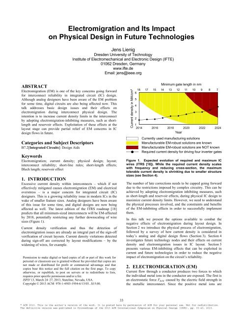
affected as well. The latest editi<strong>on</strong> of the ITRS roadmap [18]<br />
predicts that all m<strong>in</strong>imum-sized <strong>in</strong>terc<strong>on</strong>nects will be EM-affected<br />
by 2018, potentially restrict<strong>in</strong>g any further downscal<strong>in</strong>g of wire<br />
sizes (Figure 1).<br />
Current density verificati<strong>on</strong> <str<strong>on</strong>g>and</str<strong>on</strong>g> thus the detecti<strong>on</strong> of<br />
electromigrati<strong>on</strong> issues are already an <strong>in</strong>tegral part of the sign-off<br />
verificati<strong>on</strong> of circuit layouts. Current density violati<strong>on</strong>s detected<br />
dur<strong>in</strong>g sign-off are corrected by layout modificati<strong>on</strong>s – by the<br />
widen<strong>in</strong>g of wires, for example.<br />
Permissi<strong>on</strong> to make digital or hard copies of all or part of this work for<br />
pers<strong>on</strong>al or classroom use is granted without fee provided that copies are<br />
not made or distributed for profit or commercial advantage <str<strong>on</strong>g>and</str<strong>on</strong>g> that<br />
copies bear this notice <str<strong>on</strong>g>and</str<strong>on</strong>g> the full citati<strong>on</strong> <strong>on</strong> the first page. To copy<br />
otherwise, or republish, to post <strong>on</strong> servers or to redistribute to lists,<br />
requires prior specific permissi<strong>on</strong> <str<strong>on</strong>g>and</str<strong>on</strong>g>/or a fee.<br />
ISPD’13, March 24–27, 2013, Statel<strong>in</strong>e, Nevada, USA.<br />
Copyright © 2013 ACM 978-1-4503-1954-6/13/03...$15.00.<br />
Current density <strong>in</strong> MA/cm²<br />
5<br />
4<br />
3<br />
2<br />
M<strong>in</strong>imum gate length <strong>in</strong> nm<br />
18 17 15 14 13 12 11 10 9 8 7<br />
6<br />
1<br />
2014 2016 2018 2020 2022 2024<br />
Year<br />
Currently used manufactur<strong>in</strong>g soluti<strong>on</strong>s<br />
Manufacturable EM-robust soluti<strong>on</strong>s are known<br />
Manufacturable EM-robust soluti<strong>on</strong>s are NOT known<br />
Required current density for driv<strong>in</strong>g four <strong>in</strong>verter gates<br />
Figure 1. Expected evoluti<strong>on</strong> of required <str<strong>on</strong>g>and</str<strong>on</strong>g> maximum IC<br />
wires (ITRS [18]). While the required current density scales<br />
with frequency <str<strong>on</strong>g>and</str<strong>on</strong>g> reduc<strong>in</strong>g cross-secti<strong>on</strong>, the maximum<br />
tolerable current density is shr<strong>in</strong>k<strong>in</strong>g due to smaller structure<br />
sizes (see Secti<strong>on</strong> 4).<br />
The number of late correcti<strong>on</strong>s needs to be capped go<strong>in</strong>g forward<br />
due to the restricti<strong>on</strong>s imposed by complex circuitry. This can be<br />
achieved by adopt<strong>in</strong>g electromigrati<strong>on</strong> <strong>in</strong>hibit<strong>in</strong>g measures, such<br />
as short-length <str<strong>on</strong>g>and</str<strong>on</strong>g> reservoir effects, dur<strong>in</strong>g physical IC design to<br />
maximize current density limits. However, we need to underst<str<strong>on</strong>g>and</str<strong>on</strong>g><br />
the physical processes <strong>in</strong>volved, <str<strong>on</strong>g>and</str<strong>on</strong>g> the c<strong>on</strong>stra<strong>in</strong>ts <str<strong>on</strong>g>and</str<strong>on</strong>g> benefits<br />
of the EM-<strong>in</strong>hibit<strong>in</strong>g effects <strong>in</strong> order to successfully implement<br />
them.<br />
In this talk we present the opti<strong>on</strong>s available to combat the<br />
negative effects of electromigrati<strong>on</strong> dur<strong>in</strong>g layout design. In<br />
Secti<strong>on</strong> 2 we <strong>in</strong>troduce the physical process of electromigrati<strong>on</strong>,<br />
followed by a survey of how current density is c<strong>on</strong>sidered <strong>in</strong><br />
today’s analog <str<strong>on</strong>g>and</str<strong>on</strong>g> digital design flows (Secti<strong>on</strong> 3). Secti<strong>on</strong> 4<br />
<strong>in</strong>vestigates future technology nodes <str<strong>on</strong>g>and</str<strong>on</strong>g> their effects <strong>on</strong> current<br />
density <str<strong>on</strong>g>and</str<strong>on</strong>g> electromigrati<strong>on</strong> issues <strong>in</strong> IC layout. Secti<strong>on</strong> 5<br />
presents various EM-<strong>in</strong>hibit<strong>in</strong>g effects that can be exploited <strong>in</strong><br />
current <str<strong>on</strong>g>and</str<strong>on</strong>g> future technologies <strong>in</strong> order to reduce the negative<br />
impact of electromigrati<strong>on</strong> <strong>on</strong> the circuit’s reliability.<br />
2. ELECTROMIGRATION (EM)<br />
Current flow through a c<strong>on</strong>ductor produces two forces to which<br />
the <strong>in</strong>dividual metal i<strong>on</strong>s <strong>in</strong> the c<strong>on</strong>ductor are exposed. The first is<br />
an electrostatic force F field caused by the electric field strength <strong>in</strong><br />
the metallic <strong>in</strong>terc<strong>on</strong>nect. S<strong>in</strong>ce the positive metal i<strong>on</strong>s are<br />
33
shielded to some extent by the negative electr<strong>on</strong>s <strong>in</strong> the<br />
c<strong>on</strong>ductor, this force can be ignored <strong>in</strong> most cases. The sec<strong>on</strong>d<br />
force F w<strong>in</strong>d is generated by the momentum transfer between<br />
c<strong>on</strong>ducti<strong>on</strong> electr<strong>on</strong>s <str<strong>on</strong>g>and</str<strong>on</strong>g> metal i<strong>on</strong>s <strong>in</strong> the crystal lattice. This<br />
force acts <strong>in</strong> the directi<strong>on</strong> of the current flow <str<strong>on</strong>g>and</str<strong>on</strong>g> is the ma<strong>in</strong><br />
cause of electromigrati<strong>on</strong> (Figure 2).<br />
Force <strong>on</strong> metal i<strong>on</strong>s result<strong>in</strong>g<br />
from momentum transfer from<br />
the c<strong>on</strong>ducti<strong>on</strong> electr<strong>on</strong>s<br />
Anode<br />
+<br />
F w<strong>in</strong>d<br />
current-aware route plann<strong>in</strong>g [27] as well as current density<br />
verificati<strong>on</strong> [19][20].<br />
Start<br />
<strong>Physical</strong><br />
<strong>Design</strong><br />
Circuit Simulati<strong>on</strong><br />
Schematic<br />
Partiti<strong>on</strong><strong>in</strong>g + Floorplann<strong>in</strong>g<br />
Placement<br />
Current-Driven Rout<strong>in</strong>g<br />
Current-Density Verificati<strong>on</strong><br />
EM<br />
Violati<strong>on</strong>s<br />
Yes<br />
No<br />
<str<strong>on</strong>g>Electromigrati<strong>on</strong></str<strong>on</strong>g>-<br />
Robust <strong>Design</strong><br />
Current-Driven Layout<br />
Decompacti<strong>on</strong><br />
Figure 4. An electromigrati<strong>on</strong>-aware analog design flow [28].<br />
Extensive manual <strong>in</strong>terventi<strong>on</strong> <strong>in</strong> commercial synthesis tools has<br />
been needed up to now <strong>in</strong> order to <strong>in</strong>clude the impact of current<br />
densities <strong>in</strong> physical design. A first current-density-aware rout<strong>in</strong>g<br />
tool has been available from Pulsic Ltd. [12]. It widens wires<br />
based <strong>on</strong> term<strong>in</strong>al currents. It is however restricted to direct<br />
currents (DC).<br />
Verificati<strong>on</strong> tools for current densities, such as Cadence Virtuoso<br />
Power Systems [13], Synopsys CustomSim [15] <str<strong>on</strong>g>and</str<strong>on</strong>g> Apache<br />
Totem MMX [14], have been available for some time. They<br />
extract a netlist from the layout (<strong>in</strong>clud<strong>in</strong>g parasitics). This netlist<br />
is then used to simulate the currents <strong>in</strong> all wires. If any of the<br />
result<strong>in</strong>g current densities exceed an EM-relevant boundary, a<br />
violati<strong>on</strong> is detected <str<strong>on</strong>g>and</str<strong>on</strong>g> highlighted.<br />
3.2 Digital <strong>Design</strong><br />
Digital circuits are characterized by net classes that exhibit<br />
different susceptibilities to electromigrati<strong>on</strong> [30]. We can assume<br />
that power nets carry moderately c<strong>on</strong>stant currents <str<strong>on</strong>g>and</str<strong>on</strong>g> that their<br />
current directi<strong>on</strong>s are c<strong>on</strong>sistent. Clock <str<strong>on</strong>g>and</str<strong>on</strong>g> signal nets, <strong>on</strong> the<br />
other h<str<strong>on</strong>g>and</str<strong>on</strong>g>, c<strong>on</strong>duct alternat<strong>in</strong>g currents (AC). Due to self-heal<strong>in</strong>g<br />
mechanisms, these alternat<strong>in</strong>g currents affect wire lifetimes less<br />
than direct currents [29][32]. Thus, the different net classes of<br />
digital circuits require different current density limits. Bey<strong>on</strong>d<br />
that, digital circuits st<str<strong>on</strong>g>and</str<strong>on</strong>g> out because of their large number of<br />
nets. The complexity of analog circuits does not exceed a few<br />
thous<str<strong>on</strong>g>and</str<strong>on</strong>g> nets, whereas digital circuits typically have milli<strong>on</strong>s of<br />
them.<br />
Methods employed <strong>in</strong> analog design to deal with electromigrati<strong>on</strong><br />
cannot be applied <strong>in</strong> digital circuits – other soluti<strong>on</strong>s, which can<br />
h<str<strong>on</strong>g>and</str<strong>on</strong>g>le the complexity of digital designs, are needed.<br />
In pr<strong>in</strong>ciple, the digital design flow c<strong>on</strong>sists of a series of<br />
synthesis steps, which methodically c<strong>on</strong>cretize circuit geometry<br />
(Figure 5a) [23]. Simultaneously, verificati<strong>on</strong> steps ensure the<br />
circuit acquires the required electrical characteristics <str<strong>on</strong>g>and</str<strong>on</strong>g><br />
functi<strong>on</strong>s, <str<strong>on</strong>g>and</str<strong>on</strong>g> meets the reliability <str<strong>on</strong>g>and</str<strong>on</strong>g> manufacturability criteria<br />
(Figure 5b).<br />
Synthesis<br />
Logic Synthesis<br />
Partiti<strong>on</strong><strong>in</strong>g<br />
Floorplann<strong>in</strong>g<br />
Power Rout<strong>in</strong>g<br />
Global Placement<br />
Detailed Placement<br />
Clock Tree Synthesis<br />
Global Rout<strong>in</strong>g<br />
Detailed Rout<strong>in</strong>g<br />
Tim<strong>in</strong>g Closure<br />
Analysis / Verificati<strong>on</strong><br />
Formal Verificati<strong>on</strong><br />
Global Tim<strong>in</strong>g<br />
Routability Predicti<strong>on</strong><br />
Tim<strong>in</strong>g<br />
Parasitic Extracti<strong>on</strong><br />
Sign-off DRC<br />
Sign-off Tim<strong>in</strong>g<br />
Sign-off Spice Simulati<strong>on</strong><br />
EM-Specific Analysis <str<strong>on</strong>g>and</str<strong>on</strong>g><br />
Verificati<strong>on</strong><br />
Estimati<strong>on</strong> of EM-Critical<br />
Nets Based <strong>on</strong> Netlist<br />
Current Density<br />
Distributi<strong>on</strong> <strong>in</strong> Power Nets<br />
Current Density <str<strong>on</strong>g>and</str<strong>on</strong>g><br />
Temperature Estimati<strong>on</strong><br />
Sign-off DRC w/ EM Rules<br />
Sign-off Spice Simulati<strong>on</strong><br />
of Currents <strong>in</strong> Segments<br />
(a) (b) (c)<br />
Figure 5. Synthesis-analysis loops <strong>in</strong> the design flow for<br />
digital circuits. The critical steps – physical synthesis (a) <str<strong>on</strong>g>and</str<strong>on</strong>g><br />
analysis (b) – are shown, supplemented by opti<strong>on</strong>s to address<br />
current density <str<strong>on</strong>g>and</str<strong>on</strong>g> other electromigrati<strong>on</strong> issues (c).<br />
Figure 5c shows flow opti<strong>on</strong>s to analyze the impact of<br />
electromigrati<strong>on</strong> <strong>on</strong> circuit reliability. These have <strong>on</strong>ly been partly<br />
supported to date by layout tools. However, “Sign-off DRC w/ EMrules”<br />
<str<strong>on</strong>g>and</str<strong>on</strong>g> “Sign-off Spice Simulati<strong>on</strong>” with subsequent current<br />
density verificati<strong>on</strong> are now st<str<strong>on</strong>g>and</str<strong>on</strong>g>ard functi<strong>on</strong>s <strong>in</strong> state-of-the-art<br />
digital layout tools (for example, Synopsys IC Compiler, Cadence<br />
Encounter). These functi<strong>on</strong>s are also available as st<str<strong>on</strong>g>and</str<strong>on</strong>g>-al<strong>on</strong>e<br />
verificati<strong>on</strong> tools (for example, Apache Totem MMX, Mentor<br />
Calibre PERC, Tanner HiPerVerify).<br />
An early stage “Estimati<strong>on</strong> of EM-Critical Nets” is presented <strong>in</strong><br />
[21]. It determ<strong>in</strong>es the worst-case bounds <strong>on</strong> segment currents, so<br />
nets can be separated <strong>in</strong>to critical <str<strong>on</strong>g>and</str<strong>on</strong>g> n<strong>on</strong>-critical sets. Only the set<br />
of critical nets, which is typically c<strong>on</strong>siderably smaller, requires<br />
subsequent special c<strong>on</strong>siderati<strong>on</strong> dur<strong>in</strong>g layout generati<strong>on</strong>.<br />
The “<strong>in</strong>ner work<strong>in</strong>gs” of the aforementi<strong>on</strong>ed analysis steps are<br />
almost identical <strong>in</strong> the tools. They are based <strong>on</strong> three global current<br />
density limits to identify EM violati<strong>on</strong>s: maximum allowable peak,<br />
average, <str<strong>on</strong>g>and</str<strong>on</strong>g> RMS current densities. The actual current density<br />
value <strong>in</strong> each wire segment is determ<strong>in</strong>ed by transient or steady state<br />
Spice simulati<strong>on</strong>s at transistor level. EM violati<strong>on</strong>s are detected if<br />
these actual local current densities exceed a specific limit. Power<br />
<str<strong>on</strong>g>and</str<strong>on</strong>g> signal nets are verified separately.<br />
4. EM IN FUTURE TECHNOLOGIES<br />
The global trend <strong>in</strong> size reducti<strong>on</strong> leads to improved circuit<br />
performance, efficiency at higher circuit frequencies <str<strong>on</strong>g>and</str<strong>on</strong>g> smaller<br />
footpr<strong>in</strong>ts. L<strong>in</strong>e widths will c<strong>on</strong>t<strong>in</strong>ue to decrease over time, as will<br />
wire cross-secti<strong>on</strong>al areas. As shown <strong>in</strong> Table 1, the cross-secti<strong>on</strong>al<br />
area shr<strong>in</strong>ks from about 1,000 nm² <strong>in</strong> 2014 to less than 500 nm² <strong>in</strong><br />
2018. Currents are also reduced (see Table 1 <str<strong>on</strong>g>and</str<strong>on</strong>g> Figure 6, left) due<br />
to lower supply voltages <str<strong>on</strong>g>and</str<strong>on</strong>g> shr<strong>in</strong>k<strong>in</strong>g gate capacitances. However,<br />
as current reducti<strong>on</strong> is c<strong>on</strong>stra<strong>in</strong>ed by <strong>in</strong>creas<strong>in</strong>g frequencies, the<br />
more marked decrease <strong>in</strong> cross-secti<strong>on</strong>al areas (compared to current<br />
reducti<strong>on</strong>) will give rise to <strong>in</strong>creased current densities J <strong>in</strong> ICs<br />
go<strong>in</strong>g forward (Figure 6, right).<br />
To make matters worse, the maximum tolerable current densities are<br />
shr<strong>in</strong>k<strong>in</strong>g at the same time due to smaller structure sizes 1 [17]. As a<br />
result, the ITRS [18] <strong>in</strong>dicates that all m<strong>in</strong>imum-sized <strong>in</strong>terc<strong>on</strong>nects<br />
1 Small voids <str<strong>on</strong>g>and</str<strong>on</strong>g> other material defects, which could have been tolerated<br />
<strong>in</strong> earlier technology nodes, cause <strong>in</strong>creas<strong>in</strong>gly dramatic damage or<br />
resistance change to the wires with shr<strong>in</strong>k<strong>in</strong>g metal structures. Thus,<br />
maximum tolerable current densities will have to decrease <strong>in</strong> order to<br />
ma<strong>in</strong>ta<strong>in</strong> reas<strong>on</strong>able <strong>in</strong>terc<strong>on</strong>nect reliability.<br />
35
will be EM-affected by 2018, potentially limit<strong>in</strong>g any further<br />
downscal<strong>in</strong>g of wire sizes (Figure 6, yellow barrier).<br />
Furthermore, the total length of <strong>in</strong>terc<strong>on</strong>nect per IC will c<strong>on</strong>t<strong>in</strong>ue to<br />
<strong>in</strong>crease. As a c<strong>on</strong>sequence, reliability requirements per length unit<br />
of the wires need to <strong>in</strong>crease <strong>in</strong> order to ma<strong>in</strong>ta<strong>in</strong> overall IC<br />
reliability. This accepted wisdom is c<strong>on</strong>tradicted by the future<br />
decrease <strong>in</strong> <strong>in</strong>terc<strong>on</strong>nect reliability due to electromigrati<strong>on</strong> – as<br />
noted above. The ITRS thus states that no known soluti<strong>on</strong>s are<br />
available for the EM-related reliability requirements that we will<br />
face approximately 10 years from now (Figure 6, red barrier).<br />
Table 1. Predicted technology parameters based <strong>on</strong> the ITRS,<br />
2011 editi<strong>on</strong> [18]; maximum currents <str<strong>on</strong>g>and</str<strong>on</strong>g> current densities for<br />
copper at 105°C.<br />
Year 2014 2016 2018 2020 2022 2024 2026<br />
Gate length (nm) 18.41 15.34 12.78 10.65 8.88 7.40 6.16<br />
On-chip local<br />
clock frequency 4.211 4.555 4.927 5.329 5.764 6.234 6.743<br />
(GHz)<br />
DC equivalent<br />
maximum 18.14 12.96 10.33 7.36 5.53 4.45 3.52<br />
current (µA)*<br />
Metal 1 properties<br />
Width – halfpitch<br />
(nm)<br />
23.84 18.92 15.02 11.92 9.46 7.51 5.96<br />
Aspect ratio 1.9 2.0 2.0 2.0 2.1 2.1 2.2<br />
Layer thickness<br />
(nm)*<br />
45.29 37.84 30.03 23.84 19.87 15.77 13.11<br />
Cross-secti<strong>on</strong>al<br />
area (nm²)*<br />
1,079.7 716.0 451.0 284.1 187.9 118.4 78.13<br />
DC equivalent current densities (MA/cm²)<br />
Maximum<br />
tolerable current<br />
density (w/o EM<br />
4.8 3.0 1.8 1.1 0.7 0.4 0.3<br />
degradati<strong>on</strong>)**<br />
Maximum<br />
current density<br />
(soluti<strong>on</strong>s<br />
25.4 15.4 9.3 5.6 3.4 2.1 1.2<br />
unknown)**<br />
Required current<br />
density for<br />
driv<strong>in</strong>g four<br />
1.68 1.81 2.29 2.59 2.94 3.76 4.50<br />
<strong>in</strong>verter gates<br />
*) Calculated values, based <strong>on</strong> given width W, aspect ratio A/R, <str<strong>on</strong>g>and</str<strong>on</strong>g> current<br />
density J <strong>in</strong> [18], calculated as follows: layer thickness T = A/R × W, crosssecti<strong>on</strong>al<br />
area A = W × T <str<strong>on</strong>g>and</str<strong>on</strong>g> current I = J × A.<br />
**) Approximated values from the ITRS figure INTC9 [18].<br />
All rema<strong>in</strong><strong>in</strong>g values are from the ITRS 2011 editi<strong>on</strong> [18].<br />
Increased <strong>in</strong>terc<strong>on</strong>nect resistivity caused by scatter<strong>in</strong>g effects <strong>in</strong><br />
small wires will throw up further challenges [36]. Coupled with a<br />
rise <strong>in</strong> current densities, this will lead to large local temperature<br />
gradients <strong>in</strong>side the wire caused by Joule heat<strong>in</strong>g. It accelerates<br />
temperature-dependent electromigrati<strong>on</strong> <str<strong>on</strong>g>and</str<strong>on</strong>g> <strong>in</strong>troduces additi<strong>on</strong>al<br />
thermomigrati<strong>on</strong> [22][43].<br />
The tendency to replace SiO 2 with low-k dielectrics [18] with less<br />
stiffness reduces the stress-<strong>in</strong>duced atomic backflow [39], which<br />
counteracts electromigrati<strong>on</strong> <strong>in</strong> short l<strong>in</strong>es (see Secti<strong>on</strong> 5.2).<br />
Another c<strong>on</strong>sequence of this replacement is the <strong>in</strong>creased<br />
likelihood of EM-<strong>in</strong>duced compressive failures (extrusi<strong>on</strong>s) [41].<br />
Current I <strong>in</strong> µA<br />
25<br />
20<br />
15<br />
10<br />
5<br />
I max<br />
I EM<br />
0<br />
2014 2018 2022 2026<br />
Year<br />
Current density J <strong>in</strong> MA/cm²<br />
10,0<br />
1,0<br />
J max<br />
J EM<br />
0,1<br />
2014 2018 2022 2026<br />
Year<br />
Figure 6. Expected development of currents (I max , left) <str<strong>on</strong>g>and</str<strong>on</strong>g><br />
current densities (J max , right) needed for driv<strong>in</strong>g four <strong>in</strong>verter<br />
gates, accord<strong>in</strong>g to ITRS 2011 [18] (see also Table 1). EM<br />
degradati<strong>on</strong> needs to be c<strong>on</strong>sidered when cross<strong>in</strong>g the yellow<br />
barrier of currents (I EM ) <str<strong>on</strong>g>and</str<strong>on</strong>g> current densities (J EM ). As of now,<br />
manufacturable soluti<strong>on</strong>s are not known <strong>in</strong> the red area.<br />
As already menti<strong>on</strong>ed, the surge <strong>in</strong> current density is also driven<br />
by an <strong>in</strong>crease <strong>in</strong> clock frequencies (Table 1), <strong>in</strong> resp<strong>on</strong>se to the<br />
dem<str<strong>on</strong>g>and</str<strong>on</strong>g> for enhanced performance <str<strong>on</strong>g>and</str<strong>on</strong>g> made possible by smaller<br />
transistors. Although higher frequencies will neither worsen nor<br />
improve electromigrati<strong>on</strong> issues <strong>in</strong> signal or clock nets ([38], see<br />
also Secti<strong>on</strong> 5.7), they will <strong>in</strong>crease currents (<str<strong>on</strong>g>and</str<strong>on</strong>g> thus current<br />
densities) <strong>in</strong> (DC) supply nets which are already sensitive to<br />
electromigrati<strong>on</strong> <strong>in</strong> today’s technologies.<br />
5. ADDRESSING EM IN PHYSICAL<br />
DESIGN: WHAT ARE THE OPTIONS?<br />
There are a number of well-known opti<strong>on</strong>s for <strong>in</strong>fluenc<strong>in</strong>g<br />
electromigrati<strong>on</strong> <str<strong>on</strong>g>and</str<strong>on</strong>g> current density, respectively, dur<strong>in</strong>g the<br />
physical design of an electr<strong>on</strong>ic circuit.<br />
<br />
<br />
<br />
Wire material: It is known that pure copper used for Cumetallizati<strong>on</strong><br />
is more electromigrati<strong>on</strong>-robust than alum<strong>in</strong>um<br />
at low operat<strong>in</strong>g temperatures.<br />
Wire temperature: In Equati<strong>on</strong> (1), the temperature of the<br />
c<strong>on</strong>ductor appears <strong>in</strong> the exp<strong>on</strong>ent, that is, it str<strong>on</strong>gly impacts<br />
the MTTF of the <strong>in</strong>terc<strong>on</strong>nect. For an <strong>in</strong>terc<strong>on</strong>nect to rema<strong>in</strong><br />
reliable at high temperatures, the maximum tolerable current<br />
density of the c<strong>on</strong>ductor must necessarily decrease. On the<br />
other h<str<strong>on</strong>g>and</str<strong>on</strong>g>, lower<strong>in</strong>g the temperature supports higher current<br />
densities while keep<strong>in</strong>g the reliability of the wire c<strong>on</strong>stant.<br />
Wire width: Given that current density is the ratio of current<br />
I <str<strong>on</strong>g>and</str<strong>on</strong>g> cross-secti<strong>on</strong>al area A, <str<strong>on</strong>g>and</str<strong>on</strong>g> given that most process<br />
technologies assume a c<strong>on</strong>stant thickness of the pr<strong>in</strong>ted<br />
<strong>in</strong>terc<strong>on</strong>nects, it is the wire width that exerts a direct<br />
<strong>in</strong>fluence <strong>on</strong> current density: the wider the wire, the smaller<br />
the current density <str<strong>on</strong>g>and</str<strong>on</strong>g> the greater the resistance to<br />
electromigrati<strong>on</strong>.<br />
These effects have been covered <strong>in</strong> detail <strong>in</strong> [28]. They will be of<br />
limited use <strong>in</strong> new generati<strong>on</strong> technologies because they have<br />
been largely exploited <str<strong>on</strong>g>and</str<strong>on</strong>g>/or their applicati<strong>on</strong> would be counter<strong>in</strong>tuitive<br />
to the new technology node itself, that is, its reduced<br />
structure size. Hence, tolerable current density limits need to be<br />
maximized by exploit<strong>in</strong>g further electromigrati<strong>on</strong> <strong>in</strong>hibit<strong>in</strong>g<br />
factors which are described next.<br />
36
5.1 Bamboo Structure<br />
If the wire width is reduced to below the average gra<strong>in</strong> size of the<br />
wire material, the resistance to electromigrati<strong>on</strong> <strong>in</strong>creases, despite<br />
an <strong>in</strong>crease <strong>in</strong> current density. This apparent c<strong>on</strong>tradicti<strong>on</strong> is<br />
caused by the gra<strong>in</strong> boundary locati<strong>on</strong>s. In narrow wires, the gra<strong>in</strong><br />
boundary locati<strong>on</strong>s are perpendicular to the whole wire (as shown<br />
<strong>in</strong> Figure 7) form<strong>in</strong>g a bamboo like structure. As already<br />
menti<strong>on</strong>ed, material transport occurs as much <strong>in</strong> the directi<strong>on</strong> of<br />
the current flow as al<strong>on</strong>g gra<strong>in</strong> boundaries (gra<strong>in</strong> boundary<br />
diffusi<strong>on</strong>, see Secti<strong>on</strong> 2). Because gra<strong>in</strong> boundaries <strong>in</strong> this type of<br />
bamboo structure are often perpendicular to the current flow, the<br />
boundary diffusi<strong>on</strong> factor is demoted, <str<strong>on</strong>g>and</str<strong>on</strong>g> material transport is<br />
reduced accord<strong>in</strong>gly.<br />
Reliability<br />
MTTF [h]<br />
Figure 7. Reduced wire width – less than the average gra<strong>in</strong><br />
size – improves wire reliability with regard to electromigrati<strong>on</strong>.<br />
So-called bamboo wires are characterized by gra<strong>in</strong> boundaries<br />
which are perpendicular to the directi<strong>on</strong> of the electr<strong>on</strong> w<strong>in</strong>d<br />
<str<strong>on</strong>g>and</str<strong>on</strong>g> thus permit <strong>on</strong>ly limited gra<strong>in</strong> boundary diffusi<strong>on</strong>.<br />
The bamboo structure improves reliability if the self-heat<strong>in</strong>g limit<br />
of the layer is taken <strong>in</strong>to account. In order to exploit this, wire<br />
widths are deliberately kept narrow enough to ma<strong>in</strong>ta<strong>in</strong> a bamboo<br />
structure. Also the wire material can be annealed selectively<br />
dur<strong>in</strong>g IC process<strong>in</strong>g <strong>in</strong> order to support bamboo formati<strong>on</strong>.<br />
However, the maximum possible wire width for a bamboo<br />
structure, which is about 850 nm for damascene copper [2], is<br />
often too narrow for signal l<strong>in</strong>es carry<strong>in</strong>g large-magnitude<br />
currents <strong>in</strong> analog circuits or for power supply l<strong>in</strong>es. In these<br />
circumstances, slotted wires – <strong>in</strong> which rectangular holes are<br />
carved – can be used. Here, the widths of the <strong>in</strong>dividual metal<br />
structures between the slots support bamboo formati<strong>on</strong>, <str<strong>on</strong>g>and</str<strong>on</strong>g> the<br />
total width of all the metal structures meets power requirements.<br />
Based <strong>on</strong> the same pr<strong>in</strong>ciple, a f<strong>in</strong>e-gra<strong>in</strong> power mesh is often<br />
superimposed <strong>on</strong> the circuit. This mesh c<strong>on</strong>sists of a large number<br />
of wires, <str<strong>on</strong>g>and</str<strong>on</strong>g> the <strong>in</strong>dividual wire widths form a bamboo-like<br />
structure.<br />
It must be po<strong>in</strong>ted out that process anomalies often produce<br />
variati<strong>on</strong>s <strong>in</strong> wire widths – due to etch loss, lithography issues,<br />
<str<strong>on</strong>g>and</str<strong>on</strong>g> the like – <str<strong>on</strong>g>and</str<strong>on</strong>g> variati<strong>on</strong>s <strong>in</strong> wire heights – due to metal<br />
depositi<strong>on</strong> fluctuati<strong>on</strong>s, for example – as well as impact<strong>in</strong>g the via<br />
fill rate. It is vital to take these possible process fluctuati<strong>on</strong>s <strong>in</strong>to<br />
account when determ<strong>in</strong><strong>in</strong>g viable <strong>in</strong>terc<strong>on</strong>nect dimensi<strong>on</strong>s.<br />
5.2 Short-Length Effects<br />
There are also upper limits set <strong>on</strong> the length of an <strong>in</strong>terc<strong>on</strong>nect to<br />
block electromigrati<strong>on</strong>. One of them is known as the “Blech<br />
length,” <str<strong>on</strong>g>and</str<strong>on</strong>g> any wire that has a length below this threshold length<br />
(typically <strong>on</strong> the order of 5-50 m) will not fail by<br />
electromigrati<strong>on</strong>. In this scenario, mechanical stress buildup<br />
causes a reverse migrati<strong>on</strong> process which reduces, or even<br />
compensates for, the effective material flow towards the anode<br />
(Figure 8).<br />
Gra<strong>in</strong> Boundaries<br />
– Al+ Al+ Al+ Al+ Al+ +<br />
Al+<br />
e - F N1<br />
F N2 F N3<br />
F N4 F N5<br />
w<br />
e -<br />
– Al+ Al+ Al+ Al+ Al+ Al+ Al+ +<br />
e - F N1<br />
F N2 F N3<br />
F N4 F N5<br />
Equilibrium between EM <str<strong>on</strong>g>and</str<strong>on</strong>g> SM<br />
I = c<strong>on</strong>stant<br />
if L wire < “Blech length”<br />
T = c<strong>on</strong>stant<br />
– Al+ Al+ Al+ Al+<br />
Al+ Al+ +<br />
w m<strong>in</strong> … Thermal self-heat<strong>in</strong>g<br />
e -<br />
width limit<br />
w m<strong>in</strong> w MTTF_m<strong>in</strong><br />
Wire Width w [nm]<br />
w < Gra<strong>in</strong>s<br />
(Bamboo Wires)<br />
F N1<br />
F N2<br />
F N3<br />
F N4<br />
F N5<br />
<str<strong>on</strong>g>Electromigrati<strong>on</strong></str<strong>on</strong>g> (EM)<br />
Stress Migrati<strong>on</strong> (SM)<br />
Figure 8. An illustrati<strong>on</strong> of stress migrati<strong>on</strong> caused by the<br />
mechanical stress buildup <strong>in</strong> a short wire. This reversed<br />
migrati<strong>on</strong> process essentially neutralizes the material flow due<br />
to electromigrati<strong>on</strong>.<br />
Specifically, a wir<strong>in</strong>g segment is not susceptible to<br />
electromigrati<strong>on</strong> if the product of the segment’s current density J<br />
<str<strong>on</strong>g>and</str<strong>on</strong>g> the segment’s length L is less than a process-technologydependent<br />
threshold value (JL) Blech [4]. The critical product<br />
(JL) Blech , often called the “Blech immortality c<strong>on</strong>diti<strong>on</strong>,” is<br />
obta<strong>in</strong>ed from<br />
( JL)<br />
( JL)<br />
Blech<br />
<br />
<br />
z * q<br />
where Ω is the atomic volume of the wire material (cm 3 /number),<br />
∆σ is the difference <strong>in</strong> the hydrostatic stress at both ends of the<br />
segment, z* is the effective charge of the wire’s material (a<br />
measure of the momentum transfer from electr<strong>on</strong>s to the i<strong>on</strong>s of<br />
the wire’s material), q is the fundamental electr<strong>on</strong>ic charge<br />
(z*q < 0) <str<strong>on</strong>g>and</str<strong>on</strong>g> ρ is the density of the wir<strong>in</strong>g material [39].<br />
The Blech length can be <strong>in</strong>creased by deposit<strong>in</strong>g (stiff) cap layers<br />
<strong>on</strong> top of the copper metal <str<strong>on</strong>g>and</str<strong>on</strong>g> by us<strong>in</strong>g dielectrics with a higher<br />
Young’s module (i.e., higher stiffness) because both support<br />
reverse stress migrati<strong>on</strong>. However, the cap layer also needs to<br />
suppress surface diffusi<strong>on</strong> (see Secti<strong>on</strong> 5.6).<br />
Besides the Blech effect or Blech immortality c<strong>on</strong>diti<strong>on</strong> discussed<br />
above, there is another, related short-length effect. It is based <strong>on</strong><br />
void growth saturati<strong>on</strong> due to mechanical stress buildup. Voidrelated<br />
failures <strong>in</strong> wir<strong>in</strong>g segments require the void to be grown to<br />
a critical size V fail . Reverse stress migrati<strong>on</strong> <strong>in</strong> short segments,<br />
described above, can block void growth so that it cannot reach<br />
V fail (Figure 9). Specifically, the void growth with its <strong>in</strong>crease <strong>in</strong><br />
resistance ∆R does not reach the failure state marked by ∆R fail .<br />
(2)<br />
37
There is therefore a critical product (JL) sat below which<br />
immortality is obta<strong>in</strong>ed due to void growth saturati<strong>on</strong>, given by<br />
( JL)<br />
sat<br />
<br />
A R<br />
<br />
1<br />
R<br />
A<br />
1<br />
where ρ/A <str<strong>on</strong>g>and</str<strong>on</strong>g> ρ 1 /A 1 are the ratio of resistivity to cross-secti<strong>on</strong>al<br />
area of the wire material (Cu) <str<strong>on</strong>g>and</str<strong>on</strong>g> the l<strong>in</strong>er, respectively, <str<strong>on</strong>g>and</str<strong>on</strong>g> R is<br />
the <strong>in</strong>itial wire resistance [1][37][39]. The value B is the elastic<br />
bulk modulus for the material that surrounds the wir<strong>in</strong>g<br />
segment [24].<br />
fail<br />
2<br />
B<br />
<br />
z * q<br />
(3)<br />
does not actually decrease the effects of electromigrati<strong>on</strong> itself,<br />
but prol<strong>on</strong>gs the time to failure due to void growth.<br />
Reservoirs that serve as a material source typically prol<strong>on</strong>g<br />
lifetimes, <str<strong>on</strong>g>and</str<strong>on</strong>g> reservoirs that act as dom<strong>in</strong>ant s<strong>in</strong>ks for migrated<br />
<strong>in</strong>terc<strong>on</strong>nect material can degrade lifetimes. Whether a reservoir<br />
acts as s<strong>in</strong>k or source depends <strong>on</strong> the directi<strong>on</strong> of current flow<br />
(Figure 10).<br />
Metal 2<br />
Via<br />
Metal 1<br />
e -<br />
Void nucleati<strong>on</strong><br />
e -<br />
Material source<br />
Material s<strong>in</strong>k<br />
e - e -<br />
– +<br />
Cap Layer<br />
L<strong>in</strong>er Layer<br />
Void<br />
e -<br />
Stress Migrati<strong>on</strong><br />
Void<br />
– +<br />
e - 38<br />
Time<br />
Open circuit<br />
e -<br />
e -<br />
Figure 9. A stress gradient can also cause void growth<br />
saturati<strong>on</strong> <strong>in</strong> short l<strong>in</strong>e via-above (left) <str<strong>on</strong>g>and</str<strong>on</strong>g> via-below<br />
c<strong>on</strong>figurati<strong>on</strong>s (right). Note the lesser impact of voids <strong>in</strong> a viabelow<br />
c<strong>on</strong>figurati<strong>on</strong> (right, see also Secti<strong>on</strong> 5.5).<br />
It is important to note that, <strong>on</strong>ly if (JL) sat > (JL) Blech , immortality<br />
is obta<strong>in</strong>ed due to void grow saturati<strong>on</strong> <str<strong>on</strong>g>and</str<strong>on</strong>g> the wire will not fail<br />
until the void size reaches V fail . Furthermore, (JL) sat is lower for<br />
via-above than via-below copper c<strong>on</strong>figurati<strong>on</strong>s (see Secti<strong>on</strong> 5.5<br />
<str<strong>on</strong>g>and</str<strong>on</strong>g> Figure 9). It is also lower if a low-k (low-stiffness) dielectric<br />
is used <strong>in</strong>stead of SiO 2 [39]. Some of the values of the critical<br />
product (JL) for immortality obta<strong>in</strong>ed experimentally are, for<br />
example, 1,500 A/cm for Cu/SiO 2 via-above segments [8],<br />
3,700 A/cm for Cu/SiO 2 via-below segments [25] <str<strong>on</strong>g>and</str<strong>on</strong>g> 375 A/cm<br />
for Cu/low-k via-above segments [7]. Assum<strong>in</strong>g a current density<br />
J of 5 x 10 5 A/cm 2 , the latter (low) value of 375 A/cm<br />
corresp<strong>on</strong>ds to a segment length of 7.5 µm, while Cu/SiO 2 viabelow<br />
segments can have lengths of up to 74 µm.<br />
Exploit<strong>in</strong>g the critical product (JL) for immortality, however,<br />
requires knowledge of the effects of l<strong>in</strong>ked segments.<br />
Specifically, the entire <strong>in</strong>terc<strong>on</strong>nect tree, which is the set of<br />
segments that are l<strong>in</strong>ked without diffusi<strong>on</strong> barriers – that is,<br />
with<strong>in</strong> <strong>on</strong>e layer of metallizati<strong>on</strong> – needs to be <strong>in</strong>cluded <strong>in</strong> the<br />
calculati<strong>on</strong> [6][39]. Inactive segments require special attenti<strong>on</strong><br />
because they can serve as reservoir s<strong>in</strong>ks (see Secti<strong>on</strong> 5.3) [6].<br />
Start<strong>in</strong>g with the 45 nm technology node, short-length effects can<br />
be exploited to deliberately generate EM-resistant wire segments<br />
dur<strong>in</strong>g the rout<strong>in</strong>g step. This is particularly relevant for m<strong>in</strong>imumsized<br />
wires because they “automatically” become <strong>in</strong>creas<strong>in</strong>gly<br />
EM-resistant with shr<strong>in</strong>k<strong>in</strong>g feature sizes. Also, wires that are too<br />
l<strong>on</strong>g for short-length effects can be split <strong>in</strong>to shorter, more EMresistant<br />
segments by <strong>in</strong>sert<strong>in</strong>g vias. The downside is that vias are<br />
susceptible to electromigrati<strong>on</strong>, this must be c<strong>on</strong>sidered at the<br />
same time (see Secti<strong>on</strong> 5.4).<br />
5.3 Reservoir Effect<br />
The so-called “reservoir effect” [31] can significantly improve the<br />
lifetime of multiple-level <strong>in</strong>terc<strong>on</strong>nects. Increased metal-via layer<br />
overlaps enlarge the amount of <strong>in</strong>terc<strong>on</strong>nect material at <strong>on</strong>e of the<br />
prime po<strong>in</strong>ts of EM failure: below, above <str<strong>on</strong>g>and</str<strong>on</strong>g> with<strong>in</strong> the via.<br />
Reservoirs can act as sources that have to be dra<strong>in</strong>ed before voids<br />
generated by electromigrati<strong>on</strong> become critical to the circuit. This<br />
(a)<br />
Figure 10. The reservoir effect <strong>in</strong> (b) extends the lifetime of the<br />
via c<strong>on</strong>figurati<strong>on</strong> compared to a regular via without layer<br />
overlaps (a).<br />
The reservoir effect needs to be c<strong>on</strong>sidered <strong>in</strong> c<strong>on</strong>juncti<strong>on</strong> with<br />
short-length effects because any s<strong>in</strong>k effectively <strong>in</strong>creases the<br />
wire length <str<strong>on</strong>g>and</str<strong>on</strong>g> thus reduces any possible stress buildup.<br />
C<strong>on</strong>sequently, the reservoir effect is most effectively used for nets<br />
with known, directed currents because, <strong>in</strong> this case, reservoirs<br />
act<strong>in</strong>g as sources prol<strong>on</strong>g time to failure <str<strong>on</strong>g>and</str<strong>on</strong>g> s<strong>in</strong>ks can be<br />
deliberately avoided.<br />
The reservoir effect is also leveraged by us<strong>in</strong>g multiple vias (see<br />
Secti<strong>on</strong> 5.4) s<strong>in</strong>ce via arrays have a larger reservoir area than a<br />
s<strong>in</strong>gle via. Experimental results <strong>in</strong> [31] <strong>in</strong>dicate that the prol<strong>on</strong>ged<br />
lifetime achieved is more a result of the <strong>in</strong>creased reservoir area<br />
than of current shar<strong>in</strong>g between vias.<br />
5.4 Double/Multiple Vias<br />
Particular attenti<strong>on</strong> needs to be paid to vias <str<strong>on</strong>g>and</str<strong>on</strong>g> c<strong>on</strong>tact holes,<br />
because generally the ampacity of a (tungsten) via is less than that<br />
of a metal wire of the same width. Moreover, migrati<strong>on</strong> velocities<br />
<strong>in</strong> the via material, the diffusi<strong>on</strong> barrier <str<strong>on</strong>g>and</str<strong>on</strong>g> the metal wire differ.<br />
Hence, vias are <strong>on</strong>e of the prime po<strong>in</strong>ts of void nucleati<strong>on</strong> <str<strong>on</strong>g>and</str<strong>on</strong>g><br />
thus EM failure. To compensate for this <strong>in</strong>creased vulnerability<br />
<str<strong>on</strong>g>and</str<strong>on</strong>g> to address typical manufactur<strong>in</strong>g <str<strong>on</strong>g>and</str<strong>on</strong>g> yield issues, double or<br />
multiple vias are often deployed. The via array geometry is<br />
crucial here: multiple vias need to be arranged so that the<br />
result<strong>in</strong>g current flow <str<strong>on</strong>g>and</str<strong>on</strong>g> thus EM degradati<strong>on</strong> is distributed as<br />
evenly as possible throughout the parallel vias [28].<br />
5.5 Via-Above <str<strong>on</strong>g>and</str<strong>on</strong>g> Via-Below C<strong>on</strong>figurati<strong>on</strong><br />
The generati<strong>on</strong> of voids <strong>in</strong> the vic<strong>in</strong>ity of vias is str<strong>on</strong>gly<br />
<strong>in</strong>fluenced by the geometry of the via c<strong>on</strong>figurati<strong>on</strong>. Depend<strong>in</strong>g<br />
<strong>on</strong> whether a specific wire segment is c<strong>on</strong>nected from above or<br />
below, the c<strong>on</strong>figurati<strong>on</strong> is called via-above or via-below,<br />
respectively. As described above, via stacks are pr<strong>on</strong>e to void<br />
nucleati<strong>on</strong> because of the predom<strong>in</strong>ance of <strong>in</strong>terface/surface<br />
diffusi<strong>on</strong> <strong>in</strong> copper <strong>in</strong>terc<strong>on</strong>nects <str<strong>on</strong>g>and</str<strong>on</strong>g> different electromigrati<strong>on</strong><br />
drift velocities. Although this drift velocity is low <strong>in</strong> the diffusi<strong>on</strong><br />
(b)
arrier, it is higher <strong>in</strong> the adjacent copper wire <str<strong>on</strong>g>and</str<strong>on</strong>g> tungsten via.<br />
C<strong>on</strong>sequently, electr<strong>on</strong>s pass<strong>in</strong>g through the diffusi<strong>on</strong> barrier can<br />
cause voids <strong>in</strong> the material beh<strong>in</strong>d the barrier. The impact of<br />
excessive current density is a functi<strong>on</strong> of the geometry, <str<strong>on</strong>g>and</str<strong>on</strong>g> can<br />
cause a variety of damage [5][39]. Figure 11 shows that even a<br />
low-volume void causes a failure if placed directly underneath the<br />
via, whereas a void <strong>in</strong> a via-below c<strong>on</strong>figurati<strong>on</strong> has to grow<br />
larger before the <strong>in</strong>terc<strong>on</strong>nect is destroyed.<br />
Via-above C<strong>on</strong>figurati<strong>on</strong><br />
Metal1 Cu<br />
Via-below C<strong>on</strong>figurati<strong>on</strong><br />
Metal1 Cu e -<br />
e -<br />
Void<br />
Metal2 Cu<br />
Void<br />
Metal2 Cu<br />
Ta/TaN<br />
L<strong>in</strong>er Layer<br />
SiN, NSiC<br />
Cap Layer<br />
Low <br />
Dielectric<br />
Ta/TaN<br />
L<strong>in</strong>er Layer<br />
SiN, NSiC<br />
Cap Layer<br />
Low <br />
Dielectric<br />
Figure 11. Via-above <str<strong>on</strong>g>and</str<strong>on</strong>g> via-below c<strong>on</strong>figurati<strong>on</strong>s with their<br />
different damage locati<strong>on</strong>s partly due to the <strong>in</strong>terface/surface<br />
diffusi<strong>on</strong> prevalent <strong>in</strong> copper wires.<br />
5.6 Surface Coat<strong>in</strong>g / Metal Capp<strong>in</strong>g<br />
As menti<strong>on</strong>ed <strong>in</strong> Secti<strong>on</strong> 2, the Cu/cap layer <strong>in</strong>terface is the<br />
dom<strong>in</strong>ant diffusi<strong>on</strong> path for electromigrati<strong>on</strong> <strong>in</strong> submicr<strong>on</strong> copper<br />
<strong>in</strong>terc<strong>on</strong>nects. <str<strong>on</strong>g>Electromigrati<strong>on</strong></str<strong>on</strong>g> studies <strong>in</strong> copper l<strong>in</strong>e structures<br />
show that mass transport is dom<strong>in</strong>ated by diffusi<strong>on</strong> at the Cu/cap<br />
layer <strong>in</strong>terface, probably due to the presence of defects (voids)<br />
<strong>in</strong>duced by the chemical mechanical polish (CMP) process prior<br />
to cap depositi<strong>on</strong> [11][35]. The effect of a dielectric capp<strong>in</strong>g layer<br />
<strong>on</strong> <strong>in</strong>terfacial mass transport for copper <strong>in</strong>terc<strong>on</strong>nects can<br />
therefore be exploited. For that purpose cap layers which <strong>in</strong>crease<br />
activati<strong>on</strong> energies at the <strong>in</strong>terface <str<strong>on</strong>g>and</str<strong>on</strong>g> which provide a high<br />
degree of stiffness (see Secti<strong>on</strong> 5.2) will improve EM resistance.<br />
For example, Hu et al. [16] dem<strong>on</strong>strated a significant<br />
improvement <strong>in</strong> EM lifetime by coat<strong>in</strong>g the Cu surface with a th<strong>in</strong><br />
10-nm electroless layer of CoWP.<br />
5.7 Frequency Dependency<br />
The lifetime of a wire carry<strong>in</strong>g alternat<strong>in</strong>g currents (AC) is<br />
significantly l<strong>on</strong>ger than that of a wire with direct currents (DC),<br />
due to damage-heal<strong>in</strong>g effects (Figure 12). Material migrat<strong>in</strong>g <strong>in</strong><br />
<strong>on</strong>e directi<strong>on</strong> can partially migrate back to its orig<strong>in</strong>al locati<strong>on</strong><br />
under beneficial c<strong>on</strong>diti<strong>on</strong>s. C<strong>on</strong>sequently, the <strong>in</strong>terc<strong>on</strong>nect<br />
suffers less damage from electromigrati<strong>on</strong> under AC c<strong>on</strong>diti<strong>on</strong>s.<br />
Experiments <strong>in</strong> [38] reveal that the effect of self-heal<strong>in</strong>g becomes<br />
noticeable above 10 Hz <str<strong>on</strong>g>and</str<strong>on</strong>g> <strong>in</strong>creases with the switch<strong>in</strong>g<br />
frequency up to about 10 kHz where it reaches a saturati<strong>on</strong> value.<br />
There is no improvement <strong>in</strong> circuit durability at frequencies above<br />
this po<strong>in</strong>t.<br />
Tao et al. [38] report that AC lifetime at high frequencies is<br />
typically over 1,000 times l<strong>on</strong>ger for Al-2% Si <str<strong>on</strong>g>and</str<strong>on</strong>g> Al-4% Cu <str<strong>on</strong>g>and</str<strong>on</strong>g><br />
over 500 times l<strong>on</strong>ger for Cu <strong>in</strong>terc<strong>on</strong>nects.<br />
As a c<strong>on</strong>sequence, two different sets of maximum allowable<br />
current densities are comm<strong>on</strong>ly used <strong>in</strong> practical current-density<br />
verificati<strong>on</strong>, <strong>on</strong>e for signal nets with frequencies above 10 kHz<br />
<str<strong>on</strong>g>and</str<strong>on</strong>g> <strong>on</strong>e for the rema<strong>in</strong><strong>in</strong>g (DC) nets, such as power supply l<strong>in</strong>es.<br />
MTTF (AC)<br />
MTTF (DC)<br />
10 3<br />
10 2<br />
10 1<br />
10 0<br />
10 -2<br />
10 -1<br />
10 0<br />
10 1<br />
10 2<br />
10 3<br />
Frequency <strong>in</strong> Hz<br />
10 4<br />
Figure 12. Mean time to failure (MTTF) if <strong>in</strong>terc<strong>on</strong>nect is<br />
stressed by an alternat<strong>in</strong>g current (AC) compared to MTTF if a<br />
directed current (DC) is applied [38].<br />
6. OUTLOOK<br />
<str<strong>on</strong>g>Electromigrati<strong>on</strong></str<strong>on</strong>g> (EM) is becom<strong>in</strong>g an <strong>in</strong>creas<strong>in</strong>gly difficult<br />
design challenge due to higher <strong>in</strong>terc<strong>on</strong>nect current densities. The<br />
<strong>on</strong>-go<strong>in</strong>g trend <strong>in</strong> IC downscal<strong>in</strong>g is produc<strong>in</strong>g physical designs<br />
with ever-smaller feature sizes, which can easily give rise to<br />
current densities that exceed their maximum allowable value.<br />
In order to address this problem dur<strong>in</strong>g layout synthesis, this talk<br />
has focused <strong>on</strong> basic design issues that affect electromigrati<strong>on</strong><br />
dur<strong>in</strong>g <strong>in</strong>terc<strong>on</strong>nect physical design. The aim is to <strong>in</strong>crease<br />
current density limits <strong>in</strong> the <strong>in</strong>terc<strong>on</strong>nect by utiliz<strong>in</strong>g<br />
electromigrati<strong>on</strong>-<strong>in</strong>hibit<strong>in</strong>g measures, such as short-length <str<strong>on</strong>g>and</str<strong>on</strong>g><br />
reservoir effects. Exploitati<strong>on</strong> of these effects at the layout stage<br />
provides partial relief of EM c<strong>on</strong>cerns <strong>in</strong> today’s design flows.<br />
In order to use these effects <strong>in</strong> next generati<strong>on</strong> design flows, we<br />
propose establish<strong>in</strong>g a dependence between the applied current<br />
density limits <strong>on</strong> the specific circuit geometry <str<strong>on</strong>g>and</str<strong>on</strong>g> the<br />
applicati<strong>on</strong>’s missi<strong>on</strong> profile. <strong>Design</strong> tools can significantly<br />
improve the EM robustness of the generated layout by utiliz<strong>in</strong>g<br />
EM-optimized layout c<strong>on</strong>figurati<strong>on</strong>s as c<strong>on</strong>stra<strong>in</strong>ts dur<strong>in</strong>g<br />
synthesis steps, such as rout<strong>in</strong>g. We believe that this <strong>in</strong>clusi<strong>on</strong> of<br />
EM-specific requirements <strong>in</strong> the physical design can provide<br />
relief from severe reliability c<strong>on</strong>stra<strong>in</strong>ts <strong>in</strong> future technologies.<br />
ACKNOWLEDGEMENTS<br />
The author wishes to thank Matthias Thiele <str<strong>on</strong>g>and</str<strong>on</strong>g> Tilo Meister for<br />
their c<strong>on</strong>tributi<strong>on</strong>s to this paper. This work was d<strong>on</strong>e <strong>in</strong> close<br />
collaborati<strong>on</strong> with Göran Jerke at Robert Bosch GmbH <str<strong>on</strong>g>and</str<strong>on</strong>g><br />
Shanthi Siemes <str<strong>on</strong>g>and</str<strong>on</strong>g> Uwe Hahn of GlobalFoundries Inc. Their<br />
valuable practical <strong>in</strong>put is greatly appreciated.<br />
REFERENCES<br />
[1] V. K. Andleigh, V. T. Srikar, Y.-J. Park, C. V. Thomps<strong>on</strong>, “Mechanism<br />
maps for electromigrati<strong>on</strong>-<strong>in</strong>duced failure of metal <str<strong>on</strong>g>and</str<strong>on</strong>g> alloy<br />
<strong>in</strong>terc<strong>on</strong>nects,” J. Appl. Phys. 86 (1999), 6737. DOI=<br />
http://dx.doi.org/10.1063/1.371750<br />
[2] L. Arnaud, G. Tartavel, T. Berger, D. Mariolle, Y. Gobil, I. Touet,<br />
“Microstructure <str<strong>on</strong>g>and</str<strong>on</strong>g> electromigrati<strong>on</strong> <strong>in</strong> copper damascene l<strong>in</strong>es,” Proc.<br />
37th Annual Reliability Physics Symposium (1999), 263 -269. DOI=<br />
http://dx.doi.org/10.1109/RELPHY.1999.761624<br />
[3] J. R. Black, “<str<strong>on</strong>g>Electromigrati<strong>on</strong></str<strong>on</strong>g> – A brief survey <str<strong>on</strong>g>and</str<strong>on</strong>g> some recent<br />
results,” IEEE Trans. <strong>on</strong> Electr<strong>on</strong>ic Devices (April 1969), 338-347.<br />
DOI= http://dx.doi.org/10.1109/T-ED.1969.16754<br />
10 5<br />
10 6<br />
10 7<br />
10 8<br />
39
[4] I. A. Blech, “<str<strong>on</strong>g>Electromigrati<strong>on</strong></str<strong>on</strong>g> <strong>in</strong> th<strong>in</strong> alum<strong>in</strong>um films <strong>on</strong> titanium<br />
nitride,” J. Appl. Phys., vol. 47 (1976), 1203–1208.<br />
http://dx.doi.org/10.1063/1.322842<br />
[5] Z.-S. Choi, C. L. Gan, F. Wei, C. V. Thomps<strong>on</strong>, J. H. Lee, K. L. Pey,<br />
W. K. Choi, “Fatal void size comparis<strong>on</strong>s <strong>in</strong> via-below <str<strong>on</strong>g>and</str<strong>on</strong>g> via-above<br />
Cu dual-damascene <strong>in</strong>terc<strong>on</strong>nects,” MRS Proc. Materials, Technology<br />
<str<strong>on</strong>g>and</str<strong>on</strong>g> Reliability of Advanced Interc<strong>on</strong>nects, vol. 812 (2004) F7.6.<br />
DOI= http://dx.doi.org/10.1557/PROC-812-F7.6<br />
[6] C. L. Gan, C. V. Thomps<strong>on</strong>, K. L. Pey, W. K. Choi, “Experimental<br />
characterizati<strong>on</strong> <str<strong>on</strong>g>and</str<strong>on</strong>g> model<strong>in</strong>g of the reliability of 3-term<strong>in</strong>al dualdamascene<br />
Cu <strong>in</strong>terc<strong>on</strong>nect trees,” J. Appl. Phys. 94 (2003), 1222.<br />
DOI= http://dx.doi.org/10.1063/1.1585119<br />
[7] C. S. Hau-Riege, A. P. Marathe, V. Pham, “The effect of low-k ILD <strong>on</strong><br />
the electromigrati<strong>on</strong> reliability of Cu <strong>in</strong>terc<strong>on</strong>nects with different l<strong>in</strong>e<br />
lengths,” Proc. of the 41st Int. Reliability Physics Symp. (2003), 173-<br />
177. DOI= http://dx.doi.org/10.1109/RELPHY.2003.1197740<br />
[8] C. S. Hau-Riege, A. P. Marathe, V. Pham, “The effect of l<strong>in</strong>e length <strong>on</strong><br />
the electromigrati<strong>on</strong> reliability of Cu <strong>in</strong>terc<strong>on</strong>nects,” Proc. of Advanced<br />
Metallizati<strong>on</strong> C<strong>on</strong>f. (2002), 169.<br />
[9] C. S. Hau-Riege, “An <strong>in</strong>troducti<strong>on</strong> to Cu electromigrati<strong>on</strong>,” Microel.<br />
Reliab., vol. 44 (2004), 195–205. DOI=<br />
http://dx.doi.org/10.1016/j.microrel.2003.10.020<br />
[10] M. Hayashi, S. Nakano, T. Wada, “Dependence of copper <strong>in</strong>terc<strong>on</strong>nect<br />
electromigrati<strong>on</strong> phenomen<strong>on</strong> <strong>on</strong> barrier metal materials,” Microel.<br />
Reliab., vol. 43 (2003), 1545–1550. DOI=<br />
http://dx.doi.org/10.1016/S0026-2714(03)00273-7<br />
[11] J. Hohage, M. U. Lehr, V. Kahlert, “A copper-dielectric cap <strong>in</strong>terface<br />
with high resistance to electromigrati<strong>on</strong> for high performance<br />
semic<strong>on</strong>ductor devices,” Microel. Eng<strong>in</strong>eer<strong>in</strong>g (2009), 86, 408-413.<br />
DOI= http://dx.doi.org/10.1016/j.mee.2008.12.012<br />
[12] http://pulsic.com/products/pulsic-implementati<strong>on</strong>-soluti<strong>on</strong>/unityanalog-router/<br />
[13] http://www.cadence.com/products/<br />
[14] http://www.apache-da.com/products/totem/totem-mmx<br />
[15] http://www.synopsys.com/Tools/Verificati<strong>on</strong>/AMSVerificati<strong>on</strong>/Reliabi<br />
lity/Pages/customsim-<strong>in</strong>terc<strong>on</strong>nect-reliability-analysis.aspx<br />
[16] C.-K. Hu, L. Gignac, R. Rosenberg, E. L<strong>in</strong>iger, J. Rub<strong>in</strong>o, C.<br />
Sambucetti, A. Stamper, A. Domenicucci, X. Chen, “Reduced Cu<br />
<strong>in</strong>terface diffusi<strong>on</strong> by CoWP surface coat<strong>in</strong>g,” Microelectr<strong>on</strong>ic<br />
Eng<strong>in</strong>eer<strong>in</strong>g 70 (2003), 406–411. DOI=<br />
http://dx.doi.org/10.1016/S0167-9317(03)00286-7<br />
[17] C.-K. Hu, L. Gignac, R. Rosenberg, “<str<strong>on</strong>g>Electromigrati<strong>on</strong></str<strong>on</strong>g> of Cu/low<br />
dielectric c<strong>on</strong>stant <strong>in</strong>terc<strong>on</strong>nects,” Microelectr<strong>on</strong>ics <str<strong>on</strong>g>and</str<strong>on</strong>g> Reliability<br />
(2006), 46, 213 – 231. DOI=<br />
http://dx.doi.org/10.1016/j.microrel.2005.05.015<br />
[18] Internati<strong>on</strong>al Technology Roadmap for Semic<strong>on</strong>ductors (ITRS), 2011<br />
Editi<strong>on</strong>, Onl<strong>in</strong>e: www.itrs.net/reports.html, 2012<br />
[19] G. Jerke, J. Lienig, “Hierarchical current-density verificati<strong>on</strong> <strong>in</strong><br />
arbitrarily shaped metallizati<strong>on</strong> patterns of analog circuits,” IEEE<br />
Trans. <strong>on</strong> CAD of Integr. Circuits Sys., vol. 23(1) (Jan. 2004), 80–90.<br />
DOI= http://dx.doi.org/10.1109/TCAD.2003.819899<br />
[20] G. Jerke, J. Lienig, J. Scheible, “Reliability-driven layout decompacti<strong>on</strong><br />
for electromigrati<strong>on</strong> failure avoidance <strong>in</strong> complex mixed-signal IC<br />
designs,” Proc. <strong>Design</strong> Automati<strong>on</strong> C<strong>on</strong>f. (2004), 181–184. DOI=<br />
http://dx.doi.org/10.1145/996566.996618<br />
[21] G. Jerke, J. Lienig “Early-stage determ<strong>in</strong>ati<strong>on</strong> of current-density<br />
criticality <strong>in</strong> <strong>in</strong>terc<strong>on</strong>nects,” Proc. 11th IEEE Int. Int. Symp. <strong>on</strong> Quality<br />
Electr<strong>on</strong>ic <strong>Design</strong> (ISQED) (2010), 667-774. DOI=<br />
http://dx.doi.org/10.1109/ISQED.2010.5450505<br />
[22] K. J<strong>on</strong>ggook, V. C. Tyree, C. R. Crowell, “Temperature gradient effects<br />
<strong>in</strong> electromigrati<strong>on</strong> us<strong>in</strong>g an extended transiti<strong>on</strong> probability model <str<strong>on</strong>g>and</str<strong>on</strong>g><br />
temperature gradient free tests. I. Transiti<strong>on</strong> probability model,” IEEE<br />
Int. Integrated Reliability Workshop F<strong>in</strong>al Report (1999), 24 -40. DOI=<br />
http://dx.doi.org/10.1109/IRWS.1999.830555<br />
[23] A. B. Kahng, J. Lienig, I. L. Markov, J. Hu, VLSI <strong>Physical</strong> <strong>Design</strong>:<br />
From Graph Partiti<strong>on</strong><strong>in</strong>g to Tim<strong>in</strong>g Closure, Spr<strong>in</strong>ger-Verlag, Berl<strong>in</strong>,<br />
Heidelberg, New York, ISBN 978-90-481-9590-9, 2011. DOI=<br />
http://dx.doi.org/10.1007/978-90-481-9591-6<br />
[24] M. A. Korh<strong>on</strong>en, P. Børgesen, K. N. Tu, C.-Y. Li, “Stress evoluti<strong>on</strong><br />
due to electromigrati<strong>on</strong> <strong>in</strong> c<strong>on</strong>f<strong>in</strong>ed metal l<strong>in</strong>es,” J. Appl. Phys. 73<br />
(1993), 3790. DOI= http://dx.doi.org/10.1063/1.354073<br />
[25] K.-D. Lee, E. T. Ogawa, H. Matsuhashi, P. R. Justis<strong>on</strong>, K.-S. Ko, P. S.<br />
Ho, V. A. Blaschke, “<str<strong>on</strong>g>Electromigrati<strong>on</strong></str<strong>on</strong>g> critical length effect <strong>in</strong> Cu/oxide<br />
dual-damascene <strong>in</strong>terc<strong>on</strong>nects,” Appl. Phys. Lett. 79 (2001), 3236,<br />
DOI= http://dx.doi.org/10.1063/1.1418034<br />
[26] B. Li, T. D. Sullivan, T. C. Lee, D. Badami, “Reliability challenges for<br />
copper <strong>in</strong>terc<strong>on</strong>nects,” Microel. Reliab., vol. 44 (2004), 365–380. DOI=<br />
http://dx.doi.org/10.1016/j.microrel.2003.11.004<br />
[27] J. Lienig, G. Jerke, “Current-driven wire plann<strong>in</strong>g for electromigrati<strong>on</strong><br />
avoidance <strong>in</strong> analog circuits,” Proc. Asia <str<strong>on</strong>g>and</str<strong>on</strong>g> South Pacific <strong>Design</strong><br />
Automati<strong>on</strong> C<strong>on</strong>f. (2003), 783–788. DOI=<br />
http://dx.doi.org/10.1109/ASPDAC.2003.1195125<br />
[28] J. Lienig, “Introducti<strong>on</strong> to electromigrati<strong>on</strong>-aware physical design,”<br />
Proc. Int. Symp. <strong>on</strong> <strong>Physical</strong> <strong>Design</strong> (ISPD'06), (2006), 39-46. DOI=<br />
http://dx.doi.org/10.1145/1123008.1123017<br />
[29] B. K. Liew, N. W. Cheung, C. Hu, “<str<strong>on</strong>g>Electromigrati<strong>on</strong></str<strong>on</strong>g> <strong>in</strong>terc<strong>on</strong>nect<br />
lifetime under AC <str<strong>on</strong>g>and</str<strong>on</strong>g> pulse DC stress,” Proc. 27 th Int. Reliab. Phys.<br />
Symp. (IRPS) (1989), 215–219. DOI=<br />
http://dx.doi.org/10.1109/RELPHY.1989.36348<br />
[30] J. A. Maiz, “Characterizati<strong>on</strong> of electromigrati<strong>on</strong> under bidirecti<strong>on</strong>al<br />
(BC) <str<strong>on</strong>g>and</str<strong>on</strong>g> pulsed unidirecti<strong>on</strong>al (PDC) currents,” Proc. 27 th Int. Reliab.<br />
Phys. Symp. (IRPS) (1989), 220–228. DOI=<br />
http://dx.doi.org/10.1109/RELPHY.1989.36349<br />
[31] H. V. Nguyen, C. Salm, R. Wenzel, A. J. Mouthaan, F. G. Kuper,<br />
“Simulati<strong>on</strong> <str<strong>on</strong>g>and</str<strong>on</strong>g> experimental characterizati<strong>on</strong> of reservoir <str<strong>on</strong>g>and</str<strong>on</strong>g> via<br />
layout effects <strong>on</strong> electromigrati<strong>on</strong> lifetime,” Microel. Reliab., vol. 42<br />
(2002), 1421–1425. DOI= http://dx.doi.org/10.1016/S0026-<br />
2714(02)00162-2<br />
[32] D. G. Pierce, E. S. Snyder, S. E. Swans<strong>on</strong>, L. W. Irw<strong>in</strong>, “Wafer-level<br />
pulsed-DC electromigrati<strong>on</strong> resp<strong>on</strong>se at very high frequencies,” Proc.<br />
of the Int. Reliab. Phys. Symp. (RELPHY-94) (1994), 198-206. DOI=<br />
http://dx.doi.org/10.1109/RELPHY.1994.307836<br />
[33] A. G. Sabnis, “VLSI reliability,” VLSI Electr<strong>on</strong>ics—Microstructure<br />
Science, L<strong>on</strong>d<strong>on</strong>: Academic Press Ltd., vol. 22, 1990.<br />
[34] A. Scorz<strong>on</strong>i, B. Neri, C. Caprile, F. Fant<strong>in</strong>i, “<str<strong>on</strong>g>Electromigrati<strong>on</strong></str<strong>on</strong>g> <strong>in</strong> th<strong>in</strong>film<br />
<strong>in</strong>ter-c<strong>on</strong>necti<strong>on</strong> l<strong>in</strong>es: models, methods <str<strong>on</strong>g>and</str<strong>on</strong>g> results,” Material<br />
Science Reports, New York: Elsevier, vol. 7 (1991), 143–219.<br />
http://dx.doi.org/10.1016/0920-2307(91)90005-8<br />
[35] W. Shao, S. G. Mhaisalkar, T. Sritharan, A. V. Vairagar, H. J.<br />
Engelmann, O. Aubel, E. Zschech, A. M. Gusak, K. N. Tu, “Direct<br />
evidence of Cu/cap/l<strong>in</strong>er edge be<strong>in</strong>g the dom<strong>in</strong>ant electromigrati<strong>on</strong> path<br />
<strong>in</strong> dual damascene Cu <strong>in</strong>terc<strong>on</strong>nects,” Appl. Phys. Lett., 90 (2007),<br />
052106, DOI= http://dx.doi.org/10.1063/1.2437689.<br />
[36] W. Ste<strong>in</strong>högl, G. Sch<strong>in</strong>dler, G. Ste<strong>in</strong>lesberger, M. Engelhardt, “Sizedependent<br />
resistivity of metallic wires <strong>in</strong> the mesoscopic range,”<br />
<strong>Physical</strong> Review B, 66 (2002) 075414.<br />
http://dx.doi.org/10.1103/PhysRevB.66.075414<br />
[37] Z. Suo, “Stable state of <strong>in</strong>terc<strong>on</strong>nect under temperature change <str<strong>on</strong>g>and</str<strong>on</strong>g><br />
electric current,” Acta Mater. 46 (1998), 3725. DOI=<br />
http://dx.doi.org/10.1016/S1359-6454(98)00098-6<br />
[38] J. Tao, N. W. Cheung, C. Hu, “Metal electromigrati<strong>on</strong> damage heal<strong>in</strong>g<br />
under bidirecti<strong>on</strong>al current stress,” IEEE Electr<strong>on</strong> Device Letters<br />
(1993), 14, 554-556. DOI= http://dx.doi.org/10.1109/55.260787<br />
[39] C. V. Thomps<strong>on</strong>, “Us<strong>in</strong>g l<strong>in</strong>e-length effects to optimize circuit-level<br />
reliability,” 15th Int. Symp. <strong>on</strong> the <strong>Physical</strong> <str<strong>on</strong>g>and</str<strong>on</strong>g> Failure Analysis of<br />
Integrated Circuits (IPFA) (2008), 63-66. DOI=<br />
http://dx.doi.org/10.1109/IPFA.2008.4588155<br />
[40] A. V. Vairagar, S. G. Mhaisalkar, A. Krishnamoorthy,<br />
“<str<strong>on</strong>g>Electromigrati<strong>on</strong></str<strong>on</strong>g> behavior of dual-damascene Cu <strong>in</strong>terc<strong>on</strong>nects –<br />
Structure, width, <str<strong>on</strong>g>and</str<strong>on</strong>g> length dependences,” Microel. Reliab., vol. 44<br />
(2004), 747–754. DOI=<br />
http://dx.doi.org/10.1016/j.microrel.2003.12.011<br />
[41] F. L. Wei, C. L. Gan, T. L. Tan, C. S. Hau-Riege, A. P. Marathe, J. J.<br />
Vlassak, C. V. Thomps<strong>on</strong>, “<str<strong>on</strong>g>Electromigrati<strong>on</strong></str<strong>on</strong>g>-<strong>in</strong>duced extrusi<strong>on</strong> failures<br />
<strong>in</strong> Cu/low-k <strong>in</strong>terc<strong>on</strong>nects,” J. Appl. Phys. vol. 104 (2008), 023529-<br />
023529-10. DOI= http://dx.doi.org/10.1063/1.2957057<br />
[42] D. Young, A. Christou, “Failure mechanism models for<br />
electromigrati<strong>on</strong>,” IEEE Trans. <strong>on</strong> Reliability, vol. 43(2) (June 1994),<br />
186–192. DOI= http://dx.doi.org/10.1109/24.294986<br />
[43] X. Yu, K. Weide, “A study of the thermal-electrical- <str<strong>on</strong>g>and</str<strong>on</strong>g> mechanical<br />
<strong>in</strong>fluence <strong>on</strong> degradati<strong>on</strong> <strong>in</strong> an alum<strong>in</strong>um-pad structure,”<br />
Microelectr<strong>on</strong>ics <str<strong>on</strong>g>and</str<strong>on</strong>g> Reliability (1997), 37, 1545 – 1548. DOI=<br />
http://dx.doi.org/10.1016/S0026-2714(97)00105-4<br />
40