Electromigration and Its Impact on Physical Design in Future ...
Electromigration and Its Impact on Physical Design in Future ...
Electromigration and Its Impact on Physical Design in Future ...

You also want an ePaper? Increase the reach of your titles
YUMPU automatically turns print PDFs into web optimized ePapers that Google loves.
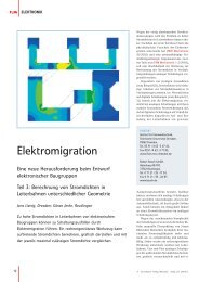
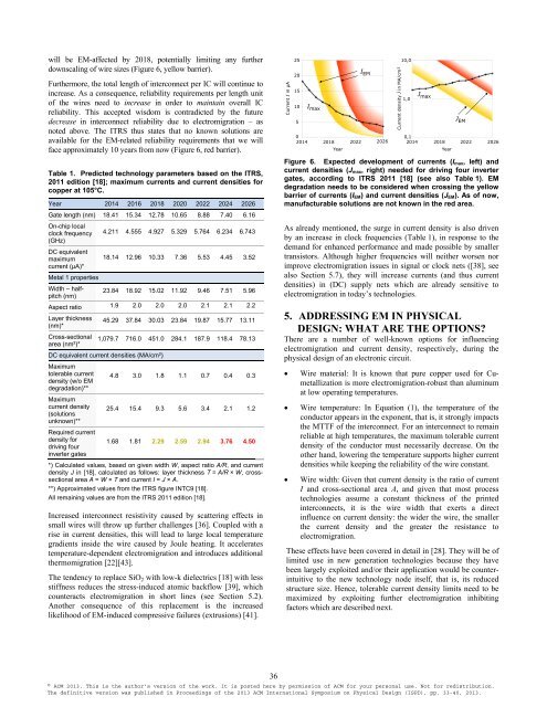
will be EM-affected by 2018, potentially limit<strong>in</strong>g any further<br />
downscal<strong>in</strong>g of wire sizes (Figure 6, yellow barrier).<br />
Furthermore, the total length of <strong>in</strong>terc<strong>on</strong>nect per IC will c<strong>on</strong>t<strong>in</strong>ue to<br />
<strong>in</strong>crease. As a c<strong>on</strong>sequence, reliability requirements per length unit<br />
of the wires need to <strong>in</strong>crease <strong>in</strong> order to ma<strong>in</strong>ta<strong>in</strong> overall IC<br />
reliability. This accepted wisdom is c<strong>on</strong>tradicted by the future<br />
decrease <strong>in</strong> <strong>in</strong>terc<strong>on</strong>nect reliability due to electromigrati<strong>on</strong> – as<br />
noted above. The ITRS thus states that no known soluti<strong>on</strong>s are<br />
available for the EM-related reliability requirements that we will<br />
face approximately 10 years from now (Figure 6, red barrier).<br />
Table 1. Predicted technology parameters based <strong>on</strong> the ITRS,<br />
2011 editi<strong>on</strong> [18]; maximum currents <str<strong>on</strong>g>and</str<strong>on</strong>g> current densities for<br />
copper at 105°C.<br />
Year 2014 2016 2018 2020 2022 2024 2026<br />
Gate length (nm) 18.41 15.34 12.78 10.65 8.88 7.40 6.16<br />
On-chip local<br />
clock frequency 4.211 4.555 4.927 5.329 5.764 6.234 6.743<br />
(GHz)<br />
DC equivalent<br />
maximum 18.14 12.96 10.33 7.36 5.53 4.45 3.52<br />
current (µA)*<br />
Metal 1 properties<br />
Width – halfpitch<br />
(nm)<br />
23.84 18.92 15.02 11.92 9.46 7.51 5.96<br />
Aspect ratio 1.9 2.0 2.0 2.0 2.1 2.1 2.2<br />
Layer thickness<br />
(nm)*<br />
45.29 37.84 30.03 23.84 19.87 15.77 13.11<br />
Cross-secti<strong>on</strong>al<br />
area (nm²)*<br />
1,079.7 716.0 451.0 284.1 187.9 118.4 78.13<br />
DC equivalent current densities (MA/cm²)<br />
Maximum<br />
tolerable current<br />
density (w/o EM<br />
4.8 3.0 1.8 1.1 0.7 0.4 0.3<br />
degradati<strong>on</strong>)**<br />
Maximum<br />
current density<br />
(soluti<strong>on</strong>s<br />
25.4 15.4 9.3 5.6 3.4 2.1 1.2<br />
unknown)**<br />
Required current<br />
density for<br />
driv<strong>in</strong>g four<br />
1.68 1.81 2.29 2.59 2.94 3.76 4.50<br />
<strong>in</strong>verter gates<br />
*) Calculated values, based <strong>on</strong> given width W, aspect ratio A/R, <str<strong>on</strong>g>and</str<strong>on</strong>g> current<br />
density J <strong>in</strong> [18], calculated as follows: layer thickness T = A/R × W, crosssecti<strong>on</strong>al<br />
area A = W × T <str<strong>on</strong>g>and</str<strong>on</strong>g> current I = J × A.<br />
**) Approximated values from the ITRS figure INTC9 [18].<br />
All rema<strong>in</strong><strong>in</strong>g values are from the ITRS 2011 editi<strong>on</strong> [18].<br />
Increased <strong>in</strong>terc<strong>on</strong>nect resistivity caused by scatter<strong>in</strong>g effects <strong>in</strong><br />
small wires will throw up further challenges [36]. Coupled with a<br />
rise <strong>in</strong> current densities, this will lead to large local temperature<br />
gradients <strong>in</strong>side the wire caused by Joule heat<strong>in</strong>g. It accelerates<br />
temperature-dependent electromigrati<strong>on</strong> <str<strong>on</strong>g>and</str<strong>on</strong>g> <strong>in</strong>troduces additi<strong>on</strong>al<br />
thermomigrati<strong>on</strong> [22][43].<br />
The tendency to replace SiO 2 with low-k dielectrics [18] with less<br />
stiffness reduces the stress-<strong>in</strong>duced atomic backflow [39], which<br />
counteracts electromigrati<strong>on</strong> <strong>in</strong> short l<strong>in</strong>es (see Secti<strong>on</strong> 5.2).<br />
Another c<strong>on</strong>sequence of this replacement is the <strong>in</strong>creased<br />
likelihood of EM-<strong>in</strong>duced compressive failures (extrusi<strong>on</strong>s) [41].<br />
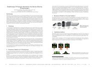
Current I <strong>in</strong> µA<br />
25<br />
20<br />
15<br />
10<br />
5<br />
I max<br />
I EM<br />
0<br />
2014 2018 2022 2026<br />
Year<br />
Current density J <strong>in</strong> MA/cm²<br />
10,0<br />
1,0<br />
J max<br />
J EM<br />
0,1<br />
2014 2018 2022 2026<br />
Year<br />
Figure 6. Expected development of currents (I max , left) <str<strong>on</strong>g>and</str<strong>on</strong>g><br />
current densities (J max , right) needed for driv<strong>in</strong>g four <strong>in</strong>verter<br />
gates, accord<strong>in</strong>g to ITRS 2011 [18] (see also Table 1). EM<br />
degradati<strong>on</strong> needs to be c<strong>on</strong>sidered when cross<strong>in</strong>g the yellow<br />
barrier of currents (I EM ) <str<strong>on</strong>g>and</str<strong>on</strong>g> current densities (J EM ). As of now,<br />
manufacturable soluti<strong>on</strong>s are not known <strong>in</strong> the red area.<br />
As already menti<strong>on</strong>ed, the surge <strong>in</strong> current density is also driven<br />
by an <strong>in</strong>crease <strong>in</strong> clock frequencies (Table 1), <strong>in</strong> resp<strong>on</strong>se to the<br />
dem<str<strong>on</strong>g>and</str<strong>on</strong>g> for enhanced performance <str<strong>on</strong>g>and</str<strong>on</strong>g> made possible by smaller<br />
transistors. Although higher frequencies will neither worsen nor<br />
improve electromigrati<strong>on</strong> issues <strong>in</strong> signal or clock nets ([38], see<br />
also Secti<strong>on</strong> 5.7), they will <strong>in</strong>crease currents (<str<strong>on</strong>g>and</str<strong>on</strong>g> thus current<br />
densities) <strong>in</strong> (DC) supply nets which are already sensitive to<br />
electromigrati<strong>on</strong> <strong>in</strong> today’s technologies.<br />
5. ADDRESSING EM IN PHYSICAL<br />
DESIGN: WHAT ARE THE OPTIONS?<br />
There are a number of well-known opti<strong>on</strong>s for <strong>in</strong>fluenc<strong>in</strong>g<br />
electromigrati<strong>on</strong> <str<strong>on</strong>g>and</str<strong>on</strong>g> current density, respectively, dur<strong>in</strong>g the<br />
physical design of an electr<strong>on</strong>ic circuit.<br />
<br />
<br />
<br />
Wire material: It is known that pure copper used for Cumetallizati<strong>on</strong><br />
is more electromigrati<strong>on</strong>-robust than alum<strong>in</strong>um<br />
at low operat<strong>in</strong>g temperatures.<br />
Wire temperature: In Equati<strong>on</strong> (1), the temperature of the<br />
c<strong>on</strong>ductor appears <strong>in</strong> the exp<strong>on</strong>ent, that is, it str<strong>on</strong>gly impacts<br />
the MTTF of the <strong>in</strong>terc<strong>on</strong>nect. For an <strong>in</strong>terc<strong>on</strong>nect to rema<strong>in</strong><br />
reliable at high temperatures, the maximum tolerable current<br />
density of the c<strong>on</strong>ductor must necessarily decrease. On the<br />
other h<str<strong>on</strong>g>and</str<strong>on</strong>g>, lower<strong>in</strong>g the temperature supports higher current<br />
densities while keep<strong>in</strong>g the reliability of the wire c<strong>on</strong>stant.<br />
Wire width: Given that current density is the ratio of current<br />
I <str<strong>on</strong>g>and</str<strong>on</strong>g> cross-secti<strong>on</strong>al area A, <str<strong>on</strong>g>and</str<strong>on</strong>g> given that most process<br />
technologies assume a c<strong>on</strong>stant thickness of the pr<strong>in</strong>ted<br />
<strong>in</strong>terc<strong>on</strong>nects, it is the wire width that exerts a direct<br />
<strong>in</strong>fluence <strong>on</strong> current density: the wider the wire, the smaller<br />
the current density <str<strong>on</strong>g>and</str<strong>on</strong>g> the greater the resistance to<br />
electromigrati<strong>on</strong>.<br />
These effects have been covered <strong>in</strong> detail <strong>in</strong> [28]. They will be of<br />
limited use <strong>in</strong> new generati<strong>on</strong> technologies because they have<br />
been largely exploited <str<strong>on</strong>g>and</str<strong>on</strong>g>/or their applicati<strong>on</strong> would be counter<strong>in</strong>tuitive<br />
to the new technology node itself, that is, its reduced<br />
structure size. Hence, tolerable current density limits need to be<br />
maximized by exploit<strong>in</strong>g further electromigrati<strong>on</strong> <strong>in</strong>hibit<strong>in</strong>g<br />
factors which are described next.<br />
36