"OPA355,2355,3355: High Speed,Video CMOS Operational Amp."
"OPA355,2355,3355: High Speed,Video CMOS Operational Amp."
"OPA355,2355,3355: High Speed,Video CMOS Operational Amp."

Create successful ePaper yourself
Turn your PDF publications into a flip-book with our unique Google optimized e-Paper software.
OPA<strong>3355</strong><br />
<strong>OPA355</strong> OPA<strong>2355</strong><br />
®<br />
OPA<strong>3355</strong><br />
<strong>OPA355</strong><br />
OPA<strong>2355</strong><br />
OPA<strong>3355</strong><br />
SBOS195B – AUGUST 2001<br />
200MHz, <strong>CMOS</strong><br />
OPERATIONAL AMPLIFIER WITH SHUTDOWN<br />
FEATURES<br />
● UNITY-GAIN BANDWIDTH: 450MHz<br />
● WIDE BANDWIDTH: 200MHz GBW<br />
● HIGH SLEW RATE: 360V/µs<br />
● LOW NOISE: 5.8nV/√Hz<br />
● EXCELLENT VIDEO PERFORMANCE:<br />
DIFF GAIN: 0.02%, DIFF PHASE: 0.05°<br />
0.1dB GAIN FLATNESS: 75MHz<br />
● INPUT RANGE INCLUDES GROUND<br />
● RAIL-TO-RAIL OUTPUT (within 100mV)<br />
● LOW INPUT BIAS CURRENT: 3pA<br />
● LOW SHUTDOWN CURRENT: 3.4µA<br />
● ENABLE/DISABLE TIME: 100ns/30ns<br />
● THERMAL SHUTDOWN<br />
● SINGLE-SUPPLY OPERATING RANGE: 2.5V to 5.5V<br />
● MicroSIZE PACKAGES<br />
APPLICATIONS<br />
DESCRIPTION<br />
The OPAx355 series high-speed, voltage-feedback <strong>CMOS</strong><br />
operational amplifiers are designed for video and other<br />
applications requiring wide bandwidth. The OPAx355 is<br />
unity gain stable and can drive large output currents. In<br />
addition, the OPAx355 has a digital shutdown (Enable)<br />
function. This feature provides power savings during idle<br />
periods and places the output in a high-impedance state to<br />
support output multiplexing. Differential gain is 0.02% and<br />
differential phase is 0.05°. Quiescent current is only 8.3mA<br />
per channel.<br />
OPAx355 is optimized for operation on single or dual<br />
supplies as low as 2.5V (±1.25V) and up to 5.5V (±2.75V).<br />
Common-mode input range for the OPAx355 extends 100mV<br />
below ground and up to 1.5V from V+. The output swing is<br />
within 100mV of the rails, supporting wide dynamic range.<br />
The OPAx355 series is available in single (SOT23-6 and<br />
SO-8), dual (MSOP-10), and triple (TSSOP-14 and SO-14)<br />
versions. Multichannel versions feature completely independent<br />
circuitry for lowest crosstalk and freedom from interaction.<br />
All are specified over the extended –40°C to 125°C<br />
range.<br />
● VIDEO PROCESSING<br />
● ULTRASOUND<br />
● OPTICAL NETWORKING, TUNABLE LASERS<br />
● PHOTODIODE TRANSIMPEDANCE AMPS<br />
● ACTIVE FILTERS<br />
● HIGH-SPEED INTEGRATORS<br />
● ANALOG-TO-DIGITAL (A/D) CONVERTER<br />
INPUT BUFFERS<br />
● DIGITAL-TO-ANALOG (D/A) CONVERTER<br />
OUTPUT AMPLIFIERS<br />
● BARCODE SCANNERS<br />
● COMMUNICATIONS<br />
OPAx355 RELATED PRODUCTS<br />
FEATURES<br />
200MHz, Rail-to-Rail Output, <strong>CMOS</strong>, No Shutdown<br />
38MHz, Rail-to-Rail Input/Output, <strong>CMOS</strong><br />
75MHz, Rail-to-Rail Output<br />
150MHz, Rail-to-Rail Output<br />
Differential Input/Output, 3.3V Supply<br />
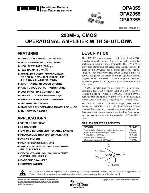
V+<br />
–V IN<br />
+V IN<br />
<strong>OPA355</strong> Out<br />
V– Enable<br />
PRODUCT<br />
OPA356<br />
OPAx350<br />
OPAx631<br />
OPAx634<br />
THS412x<br />
Please be aware that an important notice concerning availability, standard warranty, and use in critical applications of<br />
Texas Instruments semiconductor products and disclaimers thereto appears at the end of this data sheet.<br />
PRODUCTION DATA information is current as of publication date.<br />
Products conform to specifications per the terms of Texas Instruments<br />
standard warranty. Production processing does not necessarily include<br />
testing of all parameters.<br />
Copyright © 2001, Texas Instruments Incorporated<br />
www.ti.com
ABSOLUTE MAXIMUM RATINGS (1)<br />
Supply Voltage, V+ to V– ................................................................... 7.5V<br />
Signal Input Terminals, Voltage (2) .................... (V–) – 0.5V to (V+) + 0.5V<br />
Current (2) ..................................................... 10mA<br />
Enable Input ...................................................... (V–) – 0.5V to (V+) + 0.5V<br />
Output Short-Circuit (3) .............................................................. Continuous<br />
Operating Temperature .................................................. –55°C to +150°C<br />
Storage Temperature ...................................................... –65°C to +150°C<br />
Junction Temperature .................................................................... +160°C<br />
Lead Temperature (soldering, 10s) ............................................... +300°C<br />
NOTE: (1) Stresses above these ratings may cause permanent damage.<br />
Exposure to absolute maximum conditions for extended periods may degrade<br />
device reliability. These are stress ratings only, and functional operation of the<br />
device at these or any other conditions beyond those specified is not implied.<br />
(2) Input terminals are diode-clamped to the power-supply rails. Input signals<br />
that can swing more than 0.5V beyond the supply rails should be current limited<br />
to 10mA or less. (3) Short-circuit to ground one amplifier per package.<br />
ELECTROSTATIC<br />
DISCHARGE SENSITIVITY<br />
This integrated circuit can be damaged by ESD. Texas Instruments<br />
recommends that all integrated circuits be handled with<br />
appropriate precautions. Failure to observe proper handling<br />
and installation procedures can cause damage.<br />
ESD damage can range from subtle performance degradation<br />
to complete device failure. Precision integrated circuits<br />
may be more susceptible to damage because very small<br />
parametric changes could cause the device not to meet its<br />
published specifications.<br />
PACKAGE/ORDERING INFORMATION<br />
SPECIFIED<br />
PACKAGE LEAD TEMPERATURE PACKAGE ORDERING TRANSPORT<br />
PRODUCT PACKAGE DESIGNATOR COUNT RANGE MARKING NUMBER (1) MEDIA<br />
<strong>OPA355</strong>NA SOT23-6 DBV 6 –40°C to +125°C C55 <strong>OPA355</strong>NA/250 Tape and Reel<br />
" " " " " " <strong>OPA355</strong>NA/3K Tape and Reel<br />
<strong>OPA355</strong>UA SO-8 D 8 –40°C to +125°C <strong>OPA355</strong>UA <strong>OPA355</strong>UA Rails<br />
" " " " " " <strong>OPA355</strong>UA/2K5 Tape and Reel<br />
OPA<strong>2355</strong>DGSA MSOP-10 DGS 10 –40°C to +125°C D55 OPA<strong>2355</strong>DGSA/250 Tape and Reel<br />
" " " " " " OPA<strong>2355</strong>DGSA/2K5 Tape and Reel<br />
OPA<strong>3355</strong>EA TSSOP-14 PW 14 –40°C to +125°C OPA<strong>3355</strong>EA OPA<strong>3355</strong>EA/250 Tape and Reel<br />
" " " " " " OPA<strong>3355</strong>EA/2K5 Tape and Reel<br />
OPA<strong>3355</strong>UA SO-14 D 14 –40°C to +125°C OPA<strong>3355</strong>UA OPA<strong>3355</strong>UA Rails<br />
" " " " " " OPA<strong>3355</strong>UA/2K5 Tape and Reel<br />
NOTE: (1) Models with a slash (/) are available only in Tape and Reel in the quantities indicated (e.g., /2K5 indicates 2500 devices per reel). Ordering 2500 pieces<br />
of “<strong>OPA355</strong>UA/2K5” will get a single 2500-piece Tape and Reel.<br />
PIN CONFIGURATIONS<br />
Top View<br />
<strong>OPA355</strong><br />
<strong>OPA355</strong><br />
Out<br />
1<br />
6<br />
V+<br />
NC<br />
1<br />
8<br />
Enable<br />
V–<br />
2<br />
5<br />
Enable<br />
–In<br />
2<br />
7<br />
V+<br />
+In<br />
3<br />
4<br />
–In<br />
+In<br />
3<br />
6<br />
Out<br />
SOT23 (N)<br />
V–<br />
4<br />
5<br />
NC<br />
SO (U)<br />
OPA<strong>2355</strong><br />
OPA<strong>3355</strong><br />
Out A<br />
1<br />
10<br />
V+<br />
Enable A<br />
1<br />
14<br />
Out C<br />
–In A<br />
+In A<br />
V–<br />
2<br />
3<br />
4<br />
A<br />
B<br />
9<br />
8<br />
7<br />
Out B<br />
–In B<br />
+In B<br />
Enable B<br />
Enable C<br />
V+<br />
2<br />
3<br />
4<br />
C<br />
13<br />
12<br />
11<br />
–In C<br />
+In C<br />
V–<br />
Enable A<br />
5<br />
MSOP (DGS)<br />
6<br />
Enable B<br />
+In A<br />
–In A<br />
5<br />
6<br />
A<br />
B<br />
10<br />
9<br />
+In B<br />
–In B<br />
Out A<br />
7<br />
8<br />
Out B<br />
SO (U)<br />
TSSOP (E)<br />
2<br />
<strong>OPA355</strong>, <strong>2355</strong>, <strong>3355</strong><br />
SBOS195B
ELECTRICAL CHARACTERISTICS: V S = +2.7V to +5.5V Single Supply<br />
Boldface limits apply over the specified temperature range, T A = –40°C to +125°C.<br />
At T A = +25°C, R F = 604Ω, R L = 150Ω, Connected to V S /2, unless otherwise noted.<br />
<strong>OPA355</strong>NA, UA,<br />
OPA<strong>2355</strong>DGSA<br />
OPA<strong>3355</strong>EA, UA<br />
PARAMETER CONDITION MIN TYP MAX UNITS<br />
OFFSET VOLTAGE<br />
Input Offset Voltage V OS V S = +5V ±2 ±9 mV<br />
Specified Temperature Range ±15 mV<br />
vs Temperature dV OS /dT Specified Temperature Range ±7 µV/°C<br />
vs Power Supply PSRR V S = +2.7V to +5.5V, V CM = V S /2 – 0.15V ±80 ±350 µV/V<br />
INPUT BIAS CURRENT<br />
Input Bias Current I B 3 ±50 pA<br />
Input Offset Current I OS ±1 ±50 pA<br />
NOISE<br />
Input Noise Voltage Density e n f = 1MHz 5.8 nV/√Hz<br />
Current Noise Density i n f = 1MHz 50 fA/√Hz<br />
INPUT VOLTAGE RANGE<br />
Common-Mode Voltage Range V CM (V–) – 0.1 (V+) – 1.5 V<br />
Common-Mode Rejection Ratio CMRR V S = +5.5V, –0.1V < V CM < +4.0V 66 80 dB<br />
Specified Temperature Range 66 dB<br />
INPUT IMPEDANCE<br />
Differential 10 13 || 1.5 Ω || pF<br />
Common-Mode 10 13 || 1.5 Ω || pF<br />
OPEN-LOOP GAIN V S = +5V, 0.3V < V O < 4.7V 84 92 dB<br />
<strong>OPA355</strong> V S = +5V, 0.3V < V O < 4.7V 80 dB<br />
OPA<strong>2355</strong>, OPA<strong>3355</strong> V S = +5V, 0.4V < V O < 4.6V 80 dB<br />
FREQUENCY RESPONSE<br />
Small-Signal Bandwidth f –3dB G = +1, V O = 100mVp-p, R F = 0Ω 450 MHz<br />
f –3dB G = +2, V O = 100mVp-p, R L = 50Ω 100 MHz<br />
f –3dB G = +2, V O = 100mVp-p, R L = 150Ω 170 MHz<br />
f –3dB G = +2, V O = 100mVp-p, R L = 1kΩ 200 MHz<br />
Gain-Bandwidth Product GBW G = +10, R L = 1kΩ 200 MHz<br />
Bandwidth for 0.1dB Gain Flatness f 0.1dB G = +2, V O = 100mVp-p, R F = 560Ω 75 MHz<br />
Slew Rate SR V S = +5V, G = +2, 4V Output Step 300/–360 V/µs<br />
Rise-and-Fall Time G = +2, V O = 200mVp-p, 10% to 90% 2.4 ns<br />
G = +2, V O = 2Vp-p, 10% to 90% 8 ns<br />
Settling Time, 0.1% V S = +5V, G = +2, 2V Output Step 30 ns<br />
0.01% V S = +5V, G = +2, 2V Output Step 120 ns<br />
Overload Recovery Time V IN • Gain = V S 8 ns<br />
Harmonic Distortion<br />
2 nd Harmonic G = +2, f = 1MHz, V O = 2Vp-p, R L = 200Ω –81 dBc<br />
3 rd Harmonic G = +2, f = 1MHz, V O = 2Vp-p, R L = 200Ω –93 dBc<br />
Differential Gain Error NTSC, R L = 150Ω 0.02 %<br />
Differential Phase Error NTSC, R L = 150Ω 0.05 degrees<br />
Channel-to-Channel Crosstalk OPA<strong>2355</strong> f = 5MHz –90 dB<br />
OPA<strong>3355</strong> f = 5MHz –70 dB<br />
OUTPUT<br />
Voltage Output Swing from Rail V S = +5V, R L = 150Ω, A OL > 84dB 0.2 0.3 V<br />
Voltage Output Swing from Rail V S = +5V, R L = 1kΩ 0.1 V<br />
Output Current, Continuous (1) I O ±60 mA<br />
Output Current, Peak (1) I O V S = +5V ±100 mA<br />
Output Current, Peak (1) I O V S = +3V ±80 mA<br />
Closed-Loop Output Impedance f < 100kHz 0.02 Ω<br />
POWER SUPPLY<br />
Specified Voltage Range V S 2.7 5.5 V<br />
Operating Voltage Range 2.5 to 5.5 V<br />
Quiescent Current (per amplifier) I Q V S = +5V, Enabled, I O = 0 8.3 11 mA<br />
Specified Temperature Range 14 mA<br />
<strong>OPA355</strong>, <strong>2355</strong>, <strong>3355</strong> 3<br />
SBOS195B
ELECTRICAL CHARACTERISTICS: V S = +2.7V to +5.5V Single Supply (Cont.)<br />
Boldface limits apply over the specified temperature range, T A = –40°C to +125°C.<br />
At T A = +25°C, R F = 604Ω, R L = 150Ω, Connected to V S /2, unless otherwise noted.<br />
<strong>OPA355</strong>NA, UA,<br />
OPA<strong>2355</strong>DGSA<br />
OPA<strong>3355</strong>EA, UA<br />
PARAMETER CONDITION MIN TYP MAX UNITS<br />
SHUTDOWN<br />
Disable (Logic-Low Threshold) (2) 0.8 V<br />
Enable (Logic-<strong>High</strong> Threshold) (2) 2 V<br />
Enable Time 100 ns<br />
Disable Time 30 ns<br />
Shutdown Current (per amplifier) V S = +5V, Disabled 3.4 6 µA<br />
THERMAL SHUTDOWN<br />
Junction Temperature<br />
Shutdown 160 °C<br />
Reset from Shutdown 140 °C<br />
TEMPERATURE RANGE<br />
Specified Range –40 125 °C<br />
Operating Range –55 150 °C<br />
Storage Range –65 150 °C<br />
Thermal Resistance θ JA °C/W<br />
SOT-23-6, MSOP-10 150 °C/W<br />
SO-8 125 °C/W<br />
SO-14, TSSOP-14 100 °C/W<br />
NOTES: (1) See typical performance characteristic “Output Voltage Swing vs Output Current.” (2) Logic Low and <strong>High</strong> levels are <strong>CMOS</strong> logic compatible.<br />
4<br />
<strong>OPA355</strong>, <strong>2355</strong>, <strong>3355</strong><br />
SBOS195B
TYPICAL CHARACTERISTICS<br />
At T A = +25°C and V S = 5V, G = +2, R F = 604Ω, R L = 150Ω connected to V S /2, unless otherwise noted.<br />
Normalized Gain (dB)<br />
6<br />
3<br />
0<br />
–3<br />
–6<br />
–9<br />
–12<br />
V O = 0.1Vp-p<br />
NON-INVERTING SMALL-SIGNAL<br />
FREQUENCY RESPONSE<br />
G = +2<br />
G = +5<br />
G = +10<br />
G = +1<br />
R F = 0<br />
Normalized Gain (dB)<br />
3<br />
0<br />
–3<br />
–6<br />
–9<br />
–12<br />
V O = 0.1Vp-p<br />
INVERTING SMALL-SIGNAL<br />
FREQUENCY RESPONSE<br />
G = –5<br />
G = –10<br />
G = –1<br />
G = –2<br />
–15<br />
100k<br />
1M 10M 100M 1G<br />
Frequency (Hz)<br />
–15<br />
100k<br />
1M 10M 100M 1G<br />
Frequency (Hz)<br />
NON-INVERTING SMALL-SIGNAL<br />
STEP RESPONSE<br />
NON-INVERTING LARGE-SIGNAL<br />
STEP RESPONSE<br />
Output Voltage (50mV/div)<br />
G = +2<br />
Output Voltage (500mV/div)<br />
G = +2<br />
Time (20ns/div)<br />
Time (20ns/div)<br />
Output Voltage (500mV/div)<br />
LARGE-SIGNAL DISABLE/ENABLE<br />
RESPONSE<br />
f IN = 5MHz<br />
V OUT<br />
V DISABLE<br />
4.5<br />
3.5<br />
2.5<br />
1.5<br />
0.5<br />
Disable Voltage (V)<br />
Normalized Gain (dB)<br />
0.5<br />
0.4<br />
0.3<br />
0.2<br />
0.1<br />
0<br />
–0.1<br />
–0.2<br />
–0.3<br />
–0.4<br />
0.1dB GAIN FLATNESS FOR VARIOUS R F<br />
V O<br />
= 0.1Vp-p<br />
C L<br />
= 0pF<br />
R F<br />
= 560Ω<br />
R F = 500Ω<br />
R F<br />
= 604Ω<br />
Time (200ns/div)<br />
–0.5<br />
1<br />
10 100<br />
Frequency (MHz)<br />
<strong>OPA355</strong>, <strong>2355</strong>, <strong>3355</strong> 5<br />
SBOS195B
TYPICAL CHARACTERISTICS (Cont.)<br />
At T A = +25°C and V S = 5V, G = +2, R F = 604Ω, R L = 150Ω connected to V S /2, unless otherwise noted.<br />
Harmonic Distortion (dBc)<br />
–50<br />
–60<br />
–70<br />
–80<br />
–90<br />
HARMONIC DISTORTION vs OUTPUT VOLTAGE<br />
f = 1MHz<br />
R L<br />
= 200Ω<br />
2nd Harmonic<br />
3rd Harmonic<br />
Harmonic Distortion (dBc)<br />
–50<br />
–60<br />
–70<br />
–80<br />
–90<br />
HARMONIC DISTORTION vs NON-INVERTING GAIN<br />
V O<br />
= 2Vp-p<br />
f = 1MHz<br />
R L<br />
= 200Ω<br />
2nd Harmonic<br />
3rd Harmonic<br />
–100<br />
0 1<br />
2 3 4<br />
Output Voltage (Vp-p)<br />
–100<br />
1<br />
Gain (V/V)<br />
10<br />
Harmonic Distortion (dBc)<br />
–50<br />
–60<br />
–70<br />
–80<br />
–90<br />
HARMONIC DISTORTION vs INVERTING GAIN<br />
V O<br />
= 2Vp-p<br />
f = 1MHz<br />
R L<br />
= 200Ω<br />
2nd Harmonic<br />
3rd Harmonic<br />
Harmonic Distortion (dBc)<br />
–50<br />
–60<br />
–70<br />
–80<br />
–90<br />
V O<br />
= 2Vp-p<br />
R L<br />
= 200Ω<br />
HARMONIC DISTORTION vs FREQUENCY<br />
2nd Harmonic<br />
3rd Harmonic<br />
–100<br />
1<br />
Gain (V/V)<br />
10<br />
–100<br />
100k<br />
1M<br />
Frequency (Hz)<br />
10M<br />
Harmonic Distortion (dBc)<br />
–50<br />
–60<br />
–70<br />
–80<br />
–90<br />
–100<br />
100<br />
HARMONIC DISTORTION vs LOAD RESISTANCE<br />
V O = 2Vp-p<br />
f = 1MHz<br />
3rd Harmonic<br />
R L (Ω)<br />
2nd Harmonic<br />
1k<br />
Voltage Noise (nV/√Hz), Current Noise (fA/√Hz)<br />
10k<br />
1k<br />
100<br />
10<br />
INPUT VOLTAGE AND CURRENT NOISE<br />
SPECTRAL DENSITY vs FREQUENCY<br />
Voltage Noise<br />
1<br />
10 100 1k 10k 100k 1M 10M<br />
Frequency (Hz)<br />
Current Noise<br />
100M<br />
6<br />
<strong>OPA355</strong>, <strong>2355</strong>, <strong>3355</strong><br />
SBOS195B
TYPICAL CHARACTERISTICS (Cont.)<br />
At T A = +25°C and V S = 5V, G = +2, R F = 604Ω, R L = 150Ω connected to V S /2, unless otherwise noted.<br />
Normalized Gain (dB)<br />
3<br />
0<br />
–3<br />
–6<br />
–9<br />
–12<br />
FREQUENCY RESPONSE FOR VARIOUS R L<br />
C L = 0pF<br />
V O = 0.1Vp-p<br />
R L = 50Ω<br />
R L = 150Ω<br />
R L = 1kΩ<br />
R L = 10kΩ<br />
Normalized Gain (dB)<br />
9<br />
6<br />
3<br />
0<br />
–3<br />
–6<br />
–9<br />
–12<br />
FREQUENCY RESPONSE FOR VARIOUS C L<br />
R S = 0Ω<br />
V O = 0.1Vp-p<br />
C L = 100pF<br />
C L = 47pF<br />
C L = 5.6pF<br />
–15<br />
100k<br />
1M 10M 100M 1G<br />
Frequency (Hz)<br />
–15<br />
100k<br />
1M 10M 100M 1G<br />
Frequency (Hz)<br />
R S (Ω)<br />
120<br />
100<br />
80<br />
60<br />
40<br />
V IN<br />
RECOMMENDED R S vs CAPACITIVE LOAD<br />
<strong>OPA355</strong><br />
604Ω<br />
R S<br />
C L<br />
V O<br />
1kΩ<br />
Normalized Gain (dB)<br />
3<br />
0<br />
–3<br />
–6<br />
–9<br />
V IN<br />
FREQUENCY RESPONSE vs CAPACITIVE LOAD<br />
G = +2<br />
V O = 0.1Vp-p<br />
<strong>OPA355</strong><br />
604Ω<br />
C L = 100pF<br />
R S<br />
= 24Ω<br />
R S<br />
C L<br />
1kΩ<br />
V O<br />
C L = 5.6pF<br />
R S<br />
= 80Ω<br />
C L = 47pF<br />
R S = 36Ω<br />
20<br />
604Ω<br />
(1kΩ is<br />
Optional)<br />
–12<br />
604Ω<br />
(1kΩ is<br />
Optional)<br />
0<br />
1<br />
10 100<br />
Capacitive Load (pF)<br />
–15<br />
1M<br />
10M 100M 1G<br />
Frequency (Hz)<br />
CMRR, PSRR (dB)<br />
100<br />
90<br />
80<br />
70<br />
60<br />
50<br />
40<br />
30<br />
20<br />
10<br />
0<br />
10k<br />
COMMON-MODE REJECTION RATIO AND<br />
POWER-SUPPLY REJECTION RATIO vs FREQUENCY<br />
CMRR<br />
–PSRR<br />
+PSRR<br />
100k 1M 10M 100M 1G<br />
Frequency (Hz)<br />
Open-Loop Phase (degrees)<br />
Open-Loop Gain (dB)<br />
180<br />
160<br />
140<br />
120<br />
100<br />
80<br />
60<br />
40<br />
20<br />
0<br />
–20<br />
1k<br />
OPEN-LOOP GAIN AND PHASE<br />
R L = 1kΩ<br />
Phase<br />
R L<br />
= 150Ω<br />
Gain<br />
10k 100k 1M 10M 100M 1G<br />
Frequency (Hz)<br />
<strong>OPA355</strong>, <strong>2355</strong>, <strong>3355</strong> 7<br />
SBOS195B
TYPICAL CHARACTERISTICS (Cont.)<br />
At T A = +25°C and V S = 5V, G = +2, R F = 604Ω, R L = 150Ω connected to V S /2, unless otherwise noted.<br />
0.40<br />
COMPOSITE VIDEO<br />
DIFFERENTIAL GAIN AND PHASE<br />
10n<br />
INPUT BIAS CURRENT vs TEMPERATURE<br />
0.35<br />
dG/dP (%/degrees)<br />
0.30<br />
0.25<br />
0.20<br />
0.15<br />
0.10<br />
dP<br />
Input Bias Current (pA)<br />
1n<br />
100<br />
10<br />
0.05<br />
dG<br />
0<br />
1<br />
2 3<br />
4<br />
1<br />
–55 –35 –15<br />
5 25 45 65 85 105 125 135<br />
Number of 150Ω Loads<br />
Temperature (°C)<br />
3<br />
OUTPUT VOLTAGE SWING vs OUTPUT CURRENT<br />
FOR V S = 3V<br />
14<br />
SUPPLY CURRENT vs TEMPERATURE<br />
Output Voltage (V)<br />
2<br />
1<br />
125°C<br />
125°C<br />
25°C<br />
–55°C<br />
Continuous currents above<br />
60mA are not recommended.<br />
Supply Current (mA)<br />
12<br />
10<br />
8<br />
6<br />
4<br />
V S = 5.5V<br />
V S = 3V<br />
V S = 2.5V<br />
25°C<br />
–55°C<br />
2<br />
V S = 5V<br />
0<br />
0<br />
30 60 90 120 150<br />
0<br />
–55 –35 –15<br />
5 25 45 65 85 105 125 135<br />
Output Current (mA)<br />
Temperature (°C)<br />
Output Voltage (V)<br />
5<br />
4<br />
3<br />
2<br />
1<br />
OUTPUT VOLTAGE SWING vs OUTPUT CURRENT<br />
FOR V S = 5V<br />
125°C<br />
125°C<br />
25°C<br />
25°C<br />
–55°C<br />
Continuous currents above<br />
60mA are not recommended.<br />
–55°C<br />
Shutdown Current (µA)<br />
4.5<br />
4.0<br />
3.5<br />
3.0<br />
2.5<br />
2.0<br />
1.5<br />
1.0<br />
0.5<br />
SHUTDOWN CURRENT vs TEMPERATURE<br />
V S = 5.5V<br />
V S = 5V<br />
V S = 3V V S = 2.5V<br />
0<br />
0<br />
50 100 150 200 250<br />
0<br />
–55 –35 –15<br />
5 25 45 65 85 105 125 135<br />
Output Current (mA)<br />
Temperature (°C)<br />
8<br />
<strong>OPA355</strong>, <strong>2355</strong>, <strong>3355</strong><br />
SBOS195B
TYPICAL CHARACTERISTICS (Cont.)<br />
At T A = +25°C and V S = 5V, G = +2, R F = 604Ω, R L = 150Ω connected to V S /2, unless otherwise noted.<br />
100<br />
CLOSED-LOOP OUTPUT IMPEDANCE vs FREQUENCY<br />
6<br />
MAXIMUM OUTPUT VOLTAGE vs FREQUENCY<br />
V S<br />
= 5.5V<br />
Output Impedance (Ω)<br />
10<br />
1<br />
0.1<br />
0.01<br />
<strong>OPA355</strong><br />
604Ω<br />
604Ω<br />
Z O<br />
Output Voltage (Vp-p)<br />
5<br />
4<br />
3<br />
2<br />
1<br />
V S<br />
= 2.7V<br />
Maximum Output<br />
Voltage without<br />
Slew-Rate<br />
Induced Distortion<br />
0.001<br />
10k<br />
100k<br />
1M<br />
10M<br />
Frequency (Hz)<br />
100M<br />
1G<br />
0<br />
1<br />
10 100<br />
Frequency (MHz)<br />
0.2<br />
0.1<br />
V O<br />
= 2Vp-p<br />
OUTPUT SETTLING TIME TO 0.1%<br />
110<br />
100<br />
OPEN-LOOP GAIN vs TEMPERATURE<br />
R L = 1kΩ<br />
Output Error (%)<br />
0<br />
–0.1<br />
–0.2<br />
–0.3<br />
Open-Loop Gain (dB)<br />
90<br />
80<br />
70<br />
R L = 150Ω<br />
–0.4<br />
0<br />
5 10 15 20 25 30 35 40 45 50<br />
Time (ns)<br />
60<br />
–55 –35 –15<br />
5 25 45 65 85 105 125 135<br />
Temperature (°C)<br />
20<br />
OFFSET VOLTAGE PRODUCTION DISTRIBUTION<br />
100<br />
COMMON-MODE REJECTION RATIO AND<br />
POWER-SUPPLY REJECTION RATIO vs TEMPERATURE<br />
Percent of <strong>Amp</strong>lifiers (%)<br />
18<br />
16<br />
14<br />
12<br />
10<br />
8<br />
6<br />
4<br />
CMRR, PSRR (dB)<br />
90<br />
80<br />
70<br />
60<br />
Power-Supply Rejection Ratio<br />
Common-Mode Rejection Ratio<br />
2<br />
0<br />
–9 –8 –7 –6 –5 –4 –3 –2 –1 0 1 2 3 4 5 6 7 8 9<br />
50<br />
–55 –35 –15<br />
5 25 45 65 85 105 125 135<br />
Offset Voltage (mV)<br />
Temperature (°C)<br />
<strong>OPA355</strong>, <strong>2355</strong>, <strong>3355</strong> 9<br />
SBOS195B
TYPICAL CHARACTERISTICS (Cont.)<br />
At T A = +25°C and V S = 5V, G = +2, R F = 604Ω, R L = 150Ω connected to V S /2, unless otherwise noted.<br />
0<br />
CHANNEL-TO-CHANNEL CROSSTALK<br />
Crosstalk, Input-Referred (dB)<br />
–20<br />
–40<br />
–60<br />
–80<br />
–100<br />
OPA<strong>3355</strong><br />
(triple)<br />
OPA<strong>2355</strong><br />
(dual)<br />
–120<br />
100k<br />
1M<br />
Frequency (Hz)<br />
10M<br />
100M<br />
APPLICATIONS INFORMATION<br />
The OPAx355 series is a <strong>CMOS</strong>, high-speed, voltage feedback,<br />
operational amplifier designed for video and other<br />
general-purpose applications. It is available as a single, dual,<br />
or triple op amp.<br />
The amplifier features a 200MHz gain bandwidth and<br />
360V/µs slew rate, but it is unity-gain stable and can be<br />
operated as a +1V/V voltage follower.<br />
Its input common-mode voltage range includes ground,<br />
allowing the OPAx355 to be used in virtually any singlesupply<br />
application up to a supply voltage of +5.5V.<br />
PCB LAYOUT<br />
Good high-frequency PC board layout techniques should be<br />
employed for the OPAx355. Generous use of ground planes,<br />
short direct signal traces, and a suitable bypass capacitor<br />
located at the V+ pin will assure clean, stable operation.<br />
Large areas of copper also provide a means of dissipating<br />
heat that is generated within the amplifier in normal operation.<br />
Sockets are definitely not recommended for use with any<br />
high-speed amplifier.<br />
A 10µF ceramic bypass capacitor is the minimum recommended<br />
value; adding a 1µF or larger tantalum capacitor in<br />
parallel can be beneficial when driving a low-resistance<br />
load. Providing adequate bypass capacitance is essential to<br />
achieving very low harmonic and intermodulation distortion.<br />
OPERATING VOLTAGE<br />
The OPAx355 is specified over a power-supply range of<br />
+2.7V to +5.5V (±1.35 to ±2.75V). However, the supply<br />
voltage may range from +2.5V to +5.5V (±1.25V to ±2.75V).<br />
Supply voltages higher than 7.5V (absolute maximum) can<br />
permanently damage the amplifier.<br />
Parameters that vary significantly over supply voltage or<br />
temperature are shown in the “Typical Characteristics” section<br />
of this data sheet.<br />
ENABLE FUNCTION<br />
The OPAx355 can be enabled by applying a TTL “<strong>High</strong>”<br />
voltage level to the Enable pin. Conversely, a TTL “Low”<br />
voltage level will disable the amplifier, reducing its supply<br />
current from 8.3mA to only 3.4µA per amplifier. Independent<br />
Enable pins are available for each channel, providing<br />
maximum design flexibility. For portable battery-operated<br />
applications, this feature can be used to greatly reduce the<br />
average current and thereby extend battery life.<br />
10<br />
<strong>OPA355</strong>, <strong>2355</strong>, <strong>3355</strong><br />
SBOS195B
The Enable input can be modeled as a <strong>CMOS</strong> input gate with<br />
a 100kΩ pull-up resistor to V+. Left open, the Enable pin<br />
will assume a logic “<strong>High</strong>”, and the amplifier will be on.<br />
The Enable time is 100ns and the disable time is only 30ns.<br />
This allows the OPAx355 to be operated as a “gated”<br />
amplifier, or to have its output multiplexed onto a common<br />
output bus. When disabled, the output assumes a highimpedance<br />
state.<br />
OUTPUT DRIVE<br />
The OPAx355 output stage is capable of driving a standard<br />
back-terminated 75Ω video cable. By back-terminating a<br />
transmission line, it does not exhibit a capacitive load to its<br />
driver. A properly back-terminated 75Ω cable does not<br />
appear as capacitance; it presents only a 150Ω resistive load<br />
to the OPAx355 output.<br />
The output stage can supply high short-circuit current (typically<br />
over 200mA). Therefore, an on-chip thermal shutdown<br />
circuit is provided to protect the OPAx355 from dangerously<br />
high junction temperatures. At 160°C, the protection circuit<br />
will shut down the amplifier. Normal operation will resume<br />
when the junction temperature cools to below 140°C.<br />
NOTE: it is not recommended to run a continuous DC<br />
current in excess of ±60mA. Refer to the Typical Characteristics’<br />
“Output Voltage Swing vs Output Current”.<br />
INPUT AND ESD PROTECTION<br />
All OPAx355 pins are static protected with internal ESD<br />
protection diodes tied to the supplies, as shown in Figure 1.<br />
These diodes will provide overdrive protection if the current<br />
is externally limited to 10mA by the source or by a resistor.<br />
External<br />
Pin<br />
+V CC<br />
FIGURE 1. Internal ESD Protection.<br />
Internal<br />
Circuitry<br />
–V CC<br />
<strong>OPA355</strong>, <strong>2355</strong>, <strong>3355</strong> 11<br />
SBOS195B
PACKAGE DRAWINGS<br />
D (R-PDSO-G**)<br />
14 PINS SHOWN<br />
MSOI002A – JANUARY 1995 – REVISED JANUARY 1998<br />
PLASTIC SMALL-OUTLINE PACKAGE<br />
0.050 (1,27)<br />
0.020 (0,51)<br />
0.014 (0,35)<br />
0.010 (0,25)<br />
M<br />
14<br />
8<br />
0.157 (4,00)<br />
0.150 (3,81)<br />
0.244 (6,20)<br />
0.228 (5,80)<br />
0.008 (0,20) NOM<br />
Gage Plane<br />
1<br />
A<br />
7<br />
0°–8°<br />
0.010 (0,25)<br />
0.044 (1,12)<br />
0.016 (0,40)<br />
0.069 (1,75) MAX<br />
0.010 (0,25)<br />
0.004 (0,10)<br />
Seating Plane<br />
0.004 (0,10)<br />
DIM<br />
PINS **<br />
8<br />
14<br />
16<br />
A MAX<br />
0.197<br />
(5,00)<br />
0.344<br />
(8,75)<br />
0.394<br />
(10,00)<br />
A MIN<br />
0.189<br />
(4,80)<br />
0.337<br />
(8,55)<br />
0.386<br />
(9,80)<br />
4040047/ D 10/96<br />
NOTES: A. All linear dimensions are in inches (millimeters).<br />
B. This drawing is subject to change without notice.<br />
C. Body dimensions do not include mold flash or protrusion, not to exceed 0.006 (0,15).<br />
D. Falls within JEDEC MS-012<br />
12<br />
<strong>OPA355</strong>, <strong>2355</strong>, <strong>3355</strong><br />
SBOS195B
PACKAGE DRAWINGS (Cont.)<br />
DBV (R-PDSO-G6)<br />
MPDS026C – FEBRUARY 1997 – REVISED JANUARY 2001<br />
PLASTIC SMALL-OUTLINE<br />
0,95<br />
6X<br />
0,50<br />
0,25<br />
0,20<br />
M<br />
6<br />
4<br />
1,70<br />
1,50<br />
3,00<br />
2,60<br />
0,15 NOM<br />
1<br />
3,00<br />
2,80<br />
3<br />
Gage Plane<br />
0,25<br />
0°–8°<br />
0,55<br />
0,35<br />
1,45<br />
0,95<br />
0,05 MIN<br />
Seating Plane<br />
0,10<br />
4073253-5/F 10/00<br />
NOTES: A. All linear dimensions are in millimeters.<br />
B. This drawing is subject to change without notice.<br />
C. Body dimensions do not include mold flash or protrusion.<br />
D. Leads 1, 2, 3 are wider than leads 4, 5, 6 for package orientation.<br />
<strong>OPA355</strong>, <strong>2355</strong>, <strong>3355</strong> 13<br />
SBOS195B
PACKAGE DRAWINGS (Cont.)<br />
MTSS001C – JANUARY 1995 – REVISED FEBRUARY 1999<br />
PW (R-PDSO-G**)<br />
14 PINS SHOWN<br />
PLASTIC SMALL-OUTLINE PACKAGE<br />
0,30<br />
0,65 0,10 M<br />
0,19<br />
14<br />
8<br />
4,50<br />
4,30<br />
6,60<br />
6,20<br />
0,15 NOM<br />
Gage Plane<br />
1<br />
A<br />
7<br />
0°–8°<br />
0,25<br />
0,75<br />
0,50<br />
1,20 MAX<br />
0,15<br />
0,05<br />
Seating Plane<br />
0,10<br />
DIM<br />
PINS **<br />
8<br />
14<br />
16<br />
20<br />
24<br />
28<br />
A MAX<br />
3,10<br />
5,10<br />
5,10<br />
6,60<br />
7,90<br />
9,80<br />
A MIN<br />
2,90<br />
4,90<br />
4,90<br />
6,40<br />
7,70<br />
9,60<br />
4040064/F 01/97<br />
NOTES: A. All linear dimensions are in millimeters.<br />
B. This drawing is subject to change without notice.<br />
C. Body dimensions do not include mold flash or protrusion not to exceed 0,15.<br />
D. Falls within JEDEC MO-153<br />
14<br />
<strong>OPA355</strong>, <strong>2355</strong>, <strong>3355</strong><br />
SBOS195B
PACKAGE DRAWINGS (Cont.)<br />
MPDS035 – JANUARY 1998<br />
DGS (S-PDSO-G10)<br />
PLASTIC SMALL-OUTLINE PACKAGE<br />
0,27<br />
0,50 0,25 M<br />
0,17<br />
10<br />
6<br />
3,05<br />
2,95<br />
4,98<br />
4,78<br />
0,15 NOM<br />
Gage Plane<br />
0,25<br />
1<br />
3,05<br />
2,95<br />
5<br />
0°–6°<br />
0,69<br />
0,41<br />
1,07 MAX<br />
0,15<br />
0,05<br />
Seating Plane<br />
0,10<br />
4073272/A 03/98<br />
NOTES: A. All linear dimensions are in millimeters.<br />
B. This drawing is subject to change without notice.<br />
C. Body dimensions do not include mold flash or protrusion.<br />
<strong>OPA355</strong>, <strong>2355</strong>, <strong>3355</strong> 15<br />
SBOS195B
IMPORTANT NOTICE<br />
Texas Instruments Incorporated and its subsidiaries (TI) reserve the right to make corrections, modifications,<br />
enhancements, improvements, and other changes to its products and services at any time and to discontinue<br />
any product or service without notice. Customers should obtain the latest relevant information before placing<br />
orders and should verify that such information is current and complete. All products are sold subject to TI’s terms<br />
and conditions of sale supplied at the time of order acknowledgment.<br />
TI warrants performance of its hardware products to the specifications applicable at the time of sale in<br />
accordance with TI’s standard warranty. Testing and other quality control techniques are used to the extent TI<br />
deems necessary to support this warranty. Except where mandated by government requirements, testing of all<br />
parameters of each product is not necessarily performed.<br />
TI assumes no liability for applications assistance or customer product design. Customers are responsible for<br />
their products and applications using TI components. To minimize the risks associated with customer products<br />
and applications, customers should provide adequate design and operating safeguards.<br />
TI does not warrant or represent that any license, either express or implied, is granted under any TI patent right,<br />
copyright, mask work right, or other TI intellectual property right relating to any combination, machine, or process<br />
in which TI products or services are used. Information published by TI regarding third–party products or services<br />
does not constitute a license from TI to use such products or services or a warranty or endorsement thereof.<br />
Use of such information may require a license from a third party under the patents or other intellectual property<br />
of the third party, or a license from TI under the patents or other intellectual property of TI.<br />
Reproduction of information in TI data books or data sheets is permissible only if reproduction is without<br />
alteration and is accompanied by all associated warranties, conditions, limitations, and notices. Reproduction<br />
of this information with alteration is an unfair and deceptive business practice. TI is not responsible or liable for<br />
such altered documentation.<br />
Resale of TI products or services with statements different from or beyond the parameters stated by TI for that<br />
product or service voids all express and any implied warranties for the associated TI product or service and<br />
is an unfair and deceptive business practice. TI is not responsible or liable for any such statements.<br />
Mailing Address:<br />
Texas Instruments<br />
Post Office Box 655303<br />
Dallas, Texas 75265<br />
Copyright © 2001, Texas Instruments Incorporated