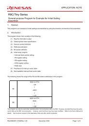
R8C/13 Group APPLICATION NOTE Flash Rewrite Using EW1 Mode
R8C/13 Group APPLICATION NOTE Flash Rewrite Using EW1 Mode
R8C/13 Group APPLICATION NOTE Flash Rewrite Using EW1 Mode

You also want an ePaper? Increase the reach of your titles
YUMPU automatically turns print PDFs into web optimized ePapers that Google loves.
<strong>APPLICATION</strong> <strong>NOTE</strong><br />
<strong>R8C</strong>/<strong>13</strong> <strong>Group</strong><br />
<strong>Flash</strong> <strong>Rewrite</strong> <strong>Using</strong> <strong>EW1</strong> <strong>Mode</strong> (Data "FFh" Search)<br />
1. Abstract<br />
This application note shows a data flash rewrite program using <strong>EW1</strong>.<br />
In this application note, Block A and Block B in flash memory are shown as data flash.<br />
2. Introduction<br />
An example described in this document supports the following microcomputer.<br />
Microcomputer<br />
: <strong>R8C</strong>/<strong>13</strong> <strong>Group</strong><br />
This program can also be used when operating other microcomputers within the <strong>R8C</strong>/Tiny series, provided they have the<br />
same SFR (Special Function Registers) and data flash as the <strong>R8C</strong>/<strong>13</strong> microcomputers. However, some functions may have<br />
been modified. Refer to the User’s Manual for details.<br />
Use functions covered in this Application Note only after careful evaluation.<br />
3. Description of Application Example<br />
3.1 <strong>Flash</strong> Memory Overview<br />
A flash memory has two rewrite modes; CPR rewrite mode and standard serial I/O mode.<br />
A CPU rewrite mode is used in this application note.<br />
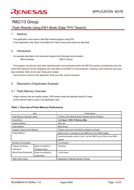
Table 1. Overview of <strong>Flash</strong> Memory Performance<br />
Item<br />
<strong>Flash</strong> Memory Operation <strong>Mode</strong><br />
Erase Block<br />
Program Method<br />
Erase Method<br />
Program, Erase Control Method<br />
Protect Method<br />
Number of Commands<br />
Program and Erase Block 0 and Block 1<br />
Endurance<br />
(Program Area)<br />
(Block Erase Endurance) Block A and Block B<br />
(Data Area)<br />
ROM Code Protect<br />
Performance<br />
2 <strong>Mode</strong>s (CPU <strong>Rewrite</strong> <strong>Mode</strong>, Standard Serial I/O <strong>Mode</strong>)<br />
See Figure 1 <strong>R8C</strong>/<strong>13</strong> Memory Map<br />
Byte Unit<br />
Block Erase<br />
Program and erase controlled by software command<br />
Blocks 0 and 1 protected by the FMR02 bit in the FMR0 register<br />
Individual protects to Block 0 and 1 by the FMR15 and 16 bits in the FMR1<br />
register<br />
5 commands<br />
100 times<br />
10,000 times<br />
Applicable for Standard Serial I/O <strong>Mode</strong><br />
REJ05B0444-0110Z/Rev.1.10 August 2004 Page 1 of 25
<strong>R8C</strong>/<strong>13</strong> <strong>Group</strong><br />
<strong>Flash</strong> <strong>Rewrite</strong> <strong>Using</strong> <strong>EW1</strong> <strong>Mode</strong> (Data "FFh" Search)<br />
Table 2. Overview of <strong>Flash</strong> Memory <strong>Rewrite</strong> <strong>Mode</strong><br />
<strong>Flash</strong> Memory <strong>Rewrite</strong> <strong>Mode</strong> CPU <strong>Rewrite</strong> <strong>Mode</strong> Standard Serial I/O <strong>Mode</strong><br />
Function<br />
User ROM area is rewritten by executing<br />
software commands from the CPU<br />
EW0 <strong>Mode</strong> : Rewritable in any area other than<br />
flash memory<br />
<strong>EW1</strong> <strong>Mode</strong> : Rewritable in flash memory<br />
User ROM area is rewritten by using a<br />
dedicated serial programmer<br />
Standard Serial I/O <strong>Mode</strong> 1:<br />
Clock Synchronous Serial I/O<br />
Standard Serial I/O <strong>Mode</strong> 2:<br />
UART<br />
Area can be rewritten User ROM Area User ROM Area<br />
Operation <strong>Mode</strong> Single Chip <strong>Mode</strong> Boot <strong>Mode</strong><br />
ROM Programmer - Serial Programmer<br />
3.2 Memory Map<br />
A user ROM area built in <strong>R8C</strong>/<strong>13</strong> consists of 4 blocks; block A, B, 0 and 1. Figure 1 shows a memory map.<br />
In this application note, a data flash ROM area of block A and B is used.<br />
02000h<br />
02800h<br />
02FFFh<br />
Block A : 2 Kbytes<br />
Block B : 2 Kbytes<br />
0C000h<br />
Block 1 : 8 Kbytes<br />
0DFFFh<br />
0E000h<br />
Block 0 : 8 Kbytes<br />
0FFFFh<br />
Figure 1. <strong>R8C</strong>/<strong>13</strong> Memory Map<br />
REJ05B0444-0110Z/Rev.1.10 August 2004 Page 2 of 25
<strong>R8C</strong>/<strong>13</strong> <strong>Group</strong><br />
<strong>Flash</strong> <strong>Rewrite</strong> <strong>Using</strong> <strong>EW1</strong> <strong>Mode</strong> (Data "FFh" Search)<br />
3.3 CPU <strong>Rewrite</strong> <strong>Mode</strong><br />
In CPU rewrite mode, the user ROM area can be rewritten by executing software commands from the CPU. Therefore, the<br />
user ROM area can be rewritten directly without using a ROM programmer, etc Execute the program and the Block Erase<br />
commands only on each block in the user ROM area.<br />
In CPU rewrite mode, the user ROM area can be operated in either erase write 0 mode (EW0 mode) and erase write 1 mode<br />
(<strong>EW1</strong> mode). Table 3 shows the difference between EW0 mode and <strong>EW1</strong> mode.<br />
<strong>EW1</strong> mode is used in this application note.<br />
Table 3. EW0 <strong>Mode</strong> and <strong>EW1</strong> <strong>Mode</strong><br />
Item EW0 <strong>Mode</strong> <strong>EW1</strong><strong>Mode</strong><br />
Operation <strong>Mode</strong> Single Chip <strong>Mode</strong> Single Chip <strong>Mode</strong><br />
Area where rewrite control User ROM Area<br />
User ROM Area<br />
program can be placed<br />
Area where rewrite control<br />
program can be executed<br />
<strong>Rewrite</strong> control program needs to be transferred<br />
to any area other than the flash memory<br />
The rewrite control program can be executed in the<br />
user ROM area<br />
(e.g., RAM)<br />
Area which can be rewritten User ROM Area User ROM Area<br />
(This excludes blocks with the rewrite control<br />
program)<br />
Software Command<br />
Restriction<br />
None<br />
⋅Program and Block Erase<br />
(Execution disabled to blocks with the rewrite<br />
control program)<br />
⋅Read status register command execution disabled<br />
<strong>Mode</strong>s after Programming Read Status Register <strong>Mode</strong><br />
Read Array <strong>Mode</strong><br />
or Erasing<br />
CPU Status during Auto<br />
Write and Auto Erase<br />
Operation<br />
Maintains Hold State<br />
(I/O ports maintain the state before the command is<br />
executed)<br />
<strong>Flash</strong> Memory Status<br />
Detection<br />
⋅ Read the FMR00, FMR06 and FMR07 bits in the<br />
FMR0 register by a program<br />
⋅ Execute the read status register command and<br />
read the SR7, SR5 and SR4 bits in the SRD<br />
register<br />
Read the FMR00, FMR06 and FMR07 bits in the<br />
FMR0 register by a program<br />
3.3.1 EW0 <strong>Mode</strong><br />
The microcomputer enters CPU rewrite mode by setting the FMR01 bit in the FMR0 register to “1” (CPU rewrite<br />
mode enabled) and is ready to accept software commands. EW0 mode is selected by setting the FMR11 bit in the<br />
FMR1 register to “0”. The software commands control programming and erasing. The FMR0 register or the SRD<br />
register indicates whether a programming or erasing operation is completed.<br />
3.3.2 <strong>EW1</strong> <strong>Mode</strong><br />
<strong>EW1</strong> mode is selected by setting the FMR11 bit to “1” (<strong>EW1</strong> mode) after the FMR01 bit is set to “1” (CPU rewrite mode<br />
enabled). The FMR0 register indicates whether a programming or erasing operation is completed. In <strong>EW1</strong> mode, do not<br />
execute the software command in the read status register.<br />
REJ05B0444-0110Z/Rev.1.10 August 2004 Page 3 of 25
<strong>R8C</strong>/<strong>13</strong> <strong>Group</strong><br />
<strong>Flash</strong> <strong>Rewrite</strong> <strong>Using</strong> <strong>EW1</strong> <strong>Mode</strong> (Data "FFh" Search)<br />
3.4 Associated Register Configuration<br />
Figure 2 shows the required registers to control flash memory<br />
<strong>Flash</strong> Memory Control Register 0<br />
b7 b6 b5 b4 b3 b2 b1 b0<br />
<strong>NOTE</strong>S :<br />
1.<br />
2.<br />
3.<br />
4.<br />
5.<br />
<strong>Flash</strong> Memory Control Register 1<br />
1 0<br />
<strong>NOTE</strong>S :<br />
1.<br />
2.<br />
3.<br />
0 0<br />
Symbol Address After reset<br />
FMR0 01B7h XX00 0001b<br />
Bit Symbol<br />
Bit Name<br />
Function<br />
RW<br />
FMR00 RY/BY Status Flag 0 : Busy (During writing or erasing) RO<br />
1 : Ready<br />
FMR01 CPU <strong>Rewrite</strong> <strong>Mode</strong> Select 0 : CPU rewrite mode disabled RW<br />
Bit (1)<br />
1 : CPU rewrite mode enabled<br />
FMR02 Block 0 and 1<br />
0 : <strong>Rewrite</strong> Disabled RW<br />
<strong>Rewrite</strong> Enable Bit (2) 1 : <strong>Rewrite</strong> Enabled<br />
FMSTP <strong>Flash</strong> Memory Stop Bit (3,5) 0 : Starts flash memory RW<br />
1 : Stops the flash memory<br />
(Enters low-power consumption state and flash<br />
memory is reset)<br />
(b5-b4)<br />
Reserved Bit<br />
Set to “0”.<br />
RW<br />
FMR06 Program Status Flag (4) 0 : Completed successfully RO<br />
1 : Teminated by error<br />
FMR07 Erase Status Flag (4) 0 : Completed successfully RO<br />
1 : Teminated by error<br />
When setting this bit to “1”, set to “1” immediately after setting it first to “0”. Do not generate an interrupt between setting the bit to “0” and setting it to “1”.<br />
Set the microcomputer in read array mode before writing to this bit.<br />
Set the FMR01 bit to “1” immediately after setting it first to “0” while the FMR01 bit is set to “1” (CPU rewrite mode enabled).<br />
Do not generate an interrupt between setting the this bit to “0” and setting it to “1”.<br />
Set this bit by a program in a space other than the flash memory.<br />
This bit is set to “0” by executing the clear status command.<br />
This bit is enabled when the FMR01 bit is set to “1” (CPU rewrite mode enabled).<br />
The FMSTP bit is set to “1” when the FMR01 bit is set to “0” (CPU rewrite mode disabled) and the FMSTP bit is set to “1”.<br />
The flash memory does not enter low-power consumption state nor is reset.<br />
b7 b6 b5 b4 b3 b2 b1 b0<br />
0 0<br />
Symbol Address After reset<br />
FMR1 01B5h 1000 000Xb<br />
Bit Symbol<br />
Bit Name<br />
Function<br />
(b0)<br />
Reserved Bit<br />
When read, its content is indeterminate.<br />
RO<br />
FMR11 <strong>EW1</strong> <strong>Mode</strong> Select Bit (1,2) 0 : EW0 mode RW<br />
(b4-b2)<br />
Reserved Bit<br />
1 : <strong>EW1</strong> mode<br />
Set to “0”.<br />
RW<br />
FMR15 Block 0 <strong>Rewrite</strong> Disabled 0 : <strong>Rewrite</strong> enabled RW<br />
Bit (2,3)<br />
1 : <strong>Rewrite</strong> disabled<br />
FMR16 Block 1 <strong>Rewrite</strong> Disabled 0 : <strong>Rewrite</strong> enabled RW<br />
(b7)<br />
Bit (2,3)<br />
Reserved Bit<br />
1 : <strong>Rewrite</strong> disabled<br />
Set to “1”.<br />
RW<br />
Set the FMR01 bit to “1” immediately after setting it first to “0” while the FMR01 bit is set to “1” (CPU rewrite mode enabled).<br />
Do not generate an interrupt between setting the this bit to “0” and setting it to “1”.<br />
When setting the FMR01 bit to “0” (CPU rewrite mode disabled), this bit is set to “0”.<br />
When the FMR01 bit is set to “1” (CPU rewrite mode enabled), the FMR15 and FMR16 bits are written.<br />
When setting this bit to “0”, set this bit to “0” immediately after setting it first to “1”.<br />
When setting this bit to “1”, set this bit to “1”.<br />
Figure 2. Associated Register<br />
REJ05B0444-0110Z/Rev.1.10 August 2004 Page 4 of 25
<strong>R8C</strong>/<strong>13</strong> <strong>Group</strong><br />
<strong>Flash</strong> <strong>Rewrite</strong> <strong>Using</strong> <strong>EW1</strong> <strong>Mode</strong> (Data "FFh" Search)<br />
3.5 Software Command<br />
The software commands are described below. Read or write the command code and data in 8-bit unit.<br />
Table 4. Software Commands<br />
Software Commands<br />
First Bus Cycle<br />
Second Bus Cycle<br />
<strong>Mode</strong> Address<br />
Data<br />
Data<br />
<strong>Mode</strong> Address<br />
(D 7 to D 0 )<br />
(D 7 to D 0 )<br />
Read Array Write × FFh<br />
Read Status Flag Write × 70h Read × SRD<br />
Clear Status Flag Write × 50h<br />
Program Write WA 40h Write WA WD<br />
Block Erase Write × 20h Write BA D0h<br />
SRD : Status Register (D 7 to D 0 )<br />
WA : Address to be written (The address specified in the first bus cycle is the same address specified in the second bus cycle)<br />
WD : 8-bit write data<br />
BA : Highest -order block address<br />
× : An even address in the user ROM area<br />
3.5.1 Read Array Command<br />
The read array command reads the flash memory.<br />
By writing “FFh” in the first bus cycle, read array mode is entered. Content of a specified address can be read in 8-bitunit after<br />
the next bus cycle. The microcomputer remains in read array mode until another command is written. Therefore, contents<br />
from multiple addresses can be read consecutively.<br />
3.5.2 Read Status Register Command<br />
The read status register command reads the SRD register.<br />
By writing “70h” in the first bus cycle, the SRD register can be read in the second bus cycle. Read an address in the user<br />
ROM area. In <strong>EW1</strong> mode, do not execute this command.<br />
3.5.3 Clear Status Register Command<br />
The clear status register command reads the SRD register.<br />
By writing “50h” in the first bus cycle, the FMR06 to FMR07 bits in the FMR0 register and the SR4 to SR5 bits in the SRD<br />
register are set to “0”.<br />
REJ05B0444-0110Z/Rev.1.10 August 2004 Page 5 of 25
<strong>R8C</strong>/<strong>13</strong> <strong>Group</strong><br />
<strong>Flash</strong> <strong>Rewrite</strong> <strong>Using</strong> <strong>EW1</strong> <strong>Mode</strong> (Data "FFh" Search)<br />
3.5.4 Program<br />
The program command writes 1-byte data to the flash memory.<br />
By writing “40h” in the first bus cycle and data to the write address in the second bus cycle, an auto programming operation<br />
(data program and verify) start. Set the address value specified in the first bus cycle to the same address as the write address<br />
specified in the second bus cycle.<br />
The FMR00 bit in the FMR0 register indicates whether an auto programming operation is completed. The FMR00 bit is set<br />
to“0” during auto programming and “1” when an auto programming operation is completed.<br />
After an auto programming is completed, the FMR06 bit in the FMR0 register indicates whether an auto programming<br />
operation is completed. Do not write additions to the programmed address. When the FMR02 bit in the FMR0 register is set<br />
to “0” (rewrite disabled) or the FMR02 bit is set to “1” (rewrite enabled) and the FMR15 bit in the FMR1 register is set to “1”<br />
(rewrite disable), the program command on the block0 can not be acknowledged. When the FMR16 bit is set to “1” (rewrite<br />
disabled), the program command on the block1 can not be acknowledged. In <strong>EW1</strong> mode, do not execute this command to<br />
any address at which the rewrite control program is located.<br />
Start<br />
Write the command code<br />
“40h” to the write address<br />
Write data to the write<br />
address<br />
FMR00 = 1?<br />
No<br />
Yes<br />
Full Status Check<br />
Program<br />
Completed<br />
Figure 3. Program Flow Chart<br />
REJ05B0444-0110Z/Rev.1.10 August 2004 Page 6 of 25
<strong>R8C</strong>/<strong>13</strong> <strong>Group</strong><br />
<strong>Flash</strong> <strong>Rewrite</strong> <strong>Using</strong> <strong>EW1</strong> <strong>Mode</strong> (Data "FFh" Search)<br />
3.5.5 Block Erase<br />
By writing “20h” in the first bus cycle and “D0h” in the second bus cycle to the highest-order address of a block, an auto<br />
erasing operation (erase and erase verify) starts in the specified block. The FMR00 bit in the FMR0 register indicates whether<br />
an auto erasing operation is completed. The FMR00 bit is set to “0” during auto erasing operation and “1” when the auto<br />
erasing operation is completed.<br />
After the auto erasing operation is completed, the FMR07 bit in the FMR0 register indicates whether the auto erasing<br />
operation is completed. When the FMR02 bit in the FMR0 register is set to “0” (rewrite disabled) or the FMR02 bit is set to “1”<br />
(rewrite enabled) and the FMR15 bit in the FMR1 register is set to “1” (rewrite disabled), the block erase command on the<br />
block0 can not be acknowledged. When the FMR16 bit is set to “1” (rewrite disabled), the block erase command on the<br />
block1 can not be acknowledged. Figure 4 shows block erase command when the erase-suspend function is not used. In<br />
<strong>EW1</strong> mode, do not execute this command on any address at which the rewrite control program is located.<br />
Start<br />
Write the command code<br />
“20h”<br />
Write “D0h” to the<br />
highest-order block address<br />
FMR00 = 1?<br />
No<br />
Yes<br />
Full Status Check<br />
Block erase<br />
completed<br />
Figure 4. Block Erase Command<br />
REJ05B0444-0110Z/Rev.1.10 August 2004 Page 7 of 25
<strong>R8C</strong>/<strong>13</strong> <strong>Group</strong><br />
<strong>Flash</strong> <strong>Rewrite</strong> <strong>Using</strong> <strong>EW1</strong> <strong>Mode</strong> (Data "FFh" Search)<br />
3.5.6 Status Register (SRD Register)<br />
The SRD register indicates the flash memory operation state and whether an erasing or programming operation is completed<br />
successfully or in error. The FMR00, FMR06 to FMR07 bits in the FMR0 register indicate the SRD register states. Table 5<br />
shows the SRD register. In EW0 mode, the SRD register can be read in the following cases:<br />
(1) Any given addresses in user ROM area are read after writing the read status register command.<br />
(2) Any given addresses in user ROM area are read when the program or block erase commands is executed until the read<br />
array command is executed.<br />
Table 5. SRD Register<br />
Bits in SRD<br />
Register<br />
Bits in FMR0<br />
Register<br />
Status Name<br />
Definition<br />
“0” “1”<br />
After Reset<br />
SR7(D 7 ) FMR00 Sequence Status Busy Ready 1<br />
SR6(D 6 ) - Reserved Bit - - -<br />
SR5(D 5 ) FMR07 Erase Status Completed<br />
successfully<br />
SR4(D 4 ) FMR06 Program Status Completed<br />
successfully<br />
Completed in<br />
error<br />
Completed in<br />
error<br />
SR3(D 3 ) - Reserved Bit - - -<br />
SR2(D 2 ) - Reserved Bit - - -<br />
SR1(D 1 ) - Reserved Bit - - -<br />
SR0(D 0 ) - Reserved Bit - - -<br />
D0 to D7 : Data buses are read when the read status register command is executed.<br />
FMR07 (SR5) to FMR06 (SR4) bits are set to “0” by executing the clear status register command.<br />
When the FMR07 bit (SR5) or FMR06 bit (SR4) is set to “1”, the program and block erase command can not be acknowledged.<br />
●Sequence Status (SR7, FMR00 bits)<br />
0<br />
0<br />
The sequence status indicates the flash memory state. This bit is set to “0” (busy) during an auto programming or auto<br />
erasing. It is set to “1” (ready) as soon as these operations are completed.<br />
●Erase Status (SR5, FMR07 bits)<br />
Refer to 3.5.7 Full Status Check.<br />
●Program Status (SR4, FMR06 bits)<br />
Refer to 3.5.7 Full Status Check.<br />
REJ05B0444-0110Z/Rev.1.10 August 2004 Page 8 of 25
<strong>R8C</strong>/<strong>13</strong> <strong>Group</strong><br />
<strong>Flash</strong> <strong>Rewrite</strong> <strong>Using</strong> <strong>EW1</strong> <strong>Mode</strong> (Data "FFh" Search)<br />
3.5.7 Full Status Check<br />
If an error occurs, the FMR06 to FMR07 bits in the FMR0 register are set to “1”, indicating a specific error. Therefore,<br />
Checking these status (full status check) indicates whether an erasing or programming operation is completed. Table 6<br />
shows the errors and FMR0 register state. Figure 5 shows a flow chart of the full status check and handling procedure for<br />
each error.<br />
Table 6. Errors and FMR0 Register State<br />
FMR0 register<br />
Error Error Occurrence Conditions<br />
(SRD register) State<br />
FMR07(SR5) FMR06(SR4)<br />
1 1 Command<br />
sequence<br />
error<br />
⋅ Command is written incorrectly<br />
⋅ A value other than “D0h” or “FFh” is written in the second bus cycle<br />
of the block erase command (1)<br />
1 0 Erase error ⋅ When the block erase command is executed and auto erasing<br />
operation is not completed correctly.<br />
0 1 Program<br />
error<br />
⋅ When the program command is executed and auto programming<br />
operation is not completed correctly.<br />
<strong>NOTE</strong>S:<br />
1. The flash memory enters read array mode by writing command code “FFh” in the second bus cycle of these commands. The<br />
command code written in the first bus cycle becomes disabled.<br />
Full status check<br />
FMR06=1<br />
and<br />
FMR07=1?<br />
No<br />
Yes<br />
Command<br />
sequence error<br />
(1) Execute the clear status register command and set these status flags to “0”.<br />
(2) Execute the command again after checking whether the command is entered correctly.<br />
FMR07=0?<br />
No<br />
Erase error<br />
Yes<br />
(1) Execute the clear status register command and set the erase status flag to “0”.<br />
(2) Execute the block erase command again.<br />
<strong>NOTE</strong>S:<br />
1. If the errors still occur, do not use that block.<br />
FMR06=0?<br />
No<br />
Program error<br />
Yes<br />
[During programming]<br />
(1) Execute the clear status register command and set the program status flag to “0”.<br />
(2) Execute the program command again.<br />
<strong>NOTE</strong>S:<br />
2. If the errors still occur, do not use that block.<br />
Full status check<br />
completed<br />
<strong>NOTE</strong>S:<br />
3. If either the FMR06 bit or FMR07 bit is set to “0”, the program and block erase commands can not be acknowledged.<br />
Execute the clear status register command before each command.<br />
Figure 5. Full Status Check and Handling Procedure for Each Error<br />
REJ05B0444-0110Z/Rev.1.10 August 2004 Page 9 of 25
<strong>R8C</strong>/<strong>13</strong> <strong>Group</strong><br />
<strong>Flash</strong> <strong>Rewrite</strong> <strong>Using</strong> <strong>EW1</strong> <strong>Mode</strong> (Data "FFh" Search)<br />
4. Program Overview<br />
Dividing the data flash areas in record-unit and how to write data sequentially are described below.<br />
This application note assumes that one record is made into 128 bytes. The block A, which is divided into 16 records from<br />
record 0 to 15, and the block B, which is divided into 16 records from record 16 to 31, are used as data area. Figure 6 shows<br />
the connection between data flash and records.<br />
02000h<br />
02080h<br />
02100h<br />
02700h<br />
02780h<br />
02800h<br />
02880h<br />
02F00h<br />
02F80h<br />
Record 0<br />
Record 1<br />
Record 2<br />
Record 14<br />
Record 15<br />
Record 16<br />
Record 17<br />
Record 30<br />
Record 31<br />
Block A<br />
Block B<br />
Figure 6. Connection between Data <strong>Flash</strong> and Records<br />
When writing data, write from the record 0 in record-unit. Erase (block erase) all contents in the block B after writing to the<br />
record 15 and erase all contents in the block A after writing to the record 31. When writing data for the next step, write to the<br />
record 0. The data which is written into the data flash is maintained after turning the power off. Therefore, in this application<br />
note, all records (empty records) which contain data of “FFh” are searched after reset start. The following is described how to<br />
search empty records.<br />
(1) Set the search pointer to the starting address in the record 0(Figure 7)<br />
Search pointer<br />
Data<br />
Data<br />
Record 0<br />
Record 1<br />
Allocate the search pointer to the<br />
starting address in the record 0<br />
Data<br />
No Data<br />
Record n-1<br />
Record n<br />
Figure 7. Allocate the Search Pointer to the Starting Address in the Record 0<br />
REJ05B0444-0110Z/Rev.1.10 August 2004 Page 10 of 25
<strong>R8C</strong>/<strong>13</strong> <strong>Group</strong><br />
<strong>Flash</strong> <strong>Rewrite</strong> <strong>Using</strong> <strong>EW1</strong> <strong>Mode</strong> (Data "FFh" Search)<br />
(2) Check whether the records which the search pointer indicates are empty records (ALL“FFh”)<br />
(3) When the records are not empty records, set the search pointer to the starting address of the next record. (Figure 8)<br />
Update search pointer<br />
Data<br />
Data<br />
Record 0<br />
Record 1<br />
Update search pointer to following<br />
records<br />
Data<br />
No Data<br />
Record n-1<br />
Record n<br />
Figure 8. Update Search Pointer<br />
(4) Execute (2) and (3) repeatedly until the empty records can be recognized or all records can be checked.<br />
(5) When the empty records are recognized, set the starting address of empty records to the data write address and<br />
memorize the block which stores the records as a block select (Figure 9).<br />
When the record n is an empty record,<br />
set the starting address of the record n<br />
to the data write address.<br />
In this figure, the block select is the<br />
block B.<br />
Data<br />
Data<br />
Record 0<br />
Record 1<br />
Block A<br />
Search pointer<br />
Data<br />
No Data<br />
Record n-1<br />
Record n<br />
Block B<br />
Figure 9. When the Empty Records are Recognized<br />
(6) When the empty record are not recognized in the both block A and B, erase the block A and set the starting address of<br />
the record 0 to the data write address. The block A is memorized as a block select.<br />
REJ05B0444-0110Z/Rev.1.10 August 2004 Page 11 of 25
<strong>R8C</strong>/<strong>13</strong> <strong>Group</strong><br />
<strong>Flash</strong> <strong>Rewrite</strong> <strong>Using</strong> <strong>EW1</strong> <strong>Mode</strong> (Data "FFh" Search)<br />
4.1 Function Table<br />
Declaring<br />
Outline<br />
Argument<br />
Use Variable<br />
(Global)<br />
Return Value<br />
Function<br />
Description<br />
void write_address_init(void)<br />
Reset write address to default<br />
Argument Type<br />
Meaning<br />
None<br />
Variable Type<br />
Contents of Use<br />
unsigned char *write_addr<br />
Initial Setting<br />
unsigned char block_select<br />
Initial Setting<br />
Return Value Type Value Meaning<br />
None<br />
Search the empty records. Set the write address (write_addr) and block select (block_select)<br />
Declaring<br />
Outline<br />
Argument<br />
Use Variable<br />
(Global)<br />
Return Value<br />
Function<br />
Description<br />
unsigned char flash_write(unsigned char *data)<br />
Data Write Control<br />
Argument Type<br />
unsigned char *data<br />
Meaning<br />
Table Starting Address of Write Data<br />
Variable Type<br />
Contents of Use<br />
unsigned char *write_addr<br />
Reference/Setting<br />
unsigned char block_select<br />
Reference/Setting<br />
Return Value Type Value Meaning<br />
COMPLETE<br />
Completed successfully<br />
unsigned char PROGRAM_ERR Write Error (1)<br />
ERASE_ERR Erase Error (1)<br />
Update the write address (write_addr) after writing the reecord data. When the block select has no<br />
empty records, erase unused blocks and change the block select (block_select).<br />
<strong>NOTE</strong>S: 1. When write or erase error occurs, PROGRAM_ERR+ERASE_ERR is indicated.<br />
Declaring<br />
Outline<br />
Argument<br />
Use Variable<br />
(Global)<br />
Return Value<br />
Function<br />
Description<br />
unsigned char block_erase(unsigned char *ers_addr)<br />
Block Erase Process<br />
Argument Type<br />
unsigned char *ers_addr<br />
Meaning<br />
Starting Address of Erase Block<br />
Variable Type<br />
Contents of Use<br />
None<br />
Return Value Type Value Meaning<br />
unsigned char<br />
COMPLETE<br />
Completed successfully<br />
ERASE_ERR<br />
Erase Error<br />
Erase the specified block in <strong>EW1</strong> mode<br />
Declaring<br />
Outline<br />
Argument<br />
Use Variable<br />
(Global)<br />
Return Value<br />
Function<br />
Description<br />
unsigned char data_write(unsigned char *write_data)<br />
Data Write Process<br />
Argument Type<br />
unsigned char *write_data<br />
Meaning<br />
Table Starting Address of Write Data<br />
Variable Type<br />
Contents of Use<br />
unsigned char *write_addr<br />
Reference<br />
Return Value Type Value Meaning<br />
unsigned char<br />
COMPLETE<br />
Completed successfully<br />
PROGRAM_ERR Write Error<br />
Write data for one record from write address (write_addr) in <strong>EW1</strong> mode.<br />
REJ05B0444-0110Z/Rev.1.10 August 2004 Page 12 of 25
<strong>R8C</strong>/<strong>13</strong> <strong>Group</strong><br />
<strong>Flash</strong> <strong>Rewrite</strong> <strong>Using</strong> <strong>EW1</strong> <strong>Mode</strong> (Data "FFh" Search)<br />
Declaring<br />
Outline<br />
Argument<br />
Use Variable<br />
Return Value<br />
Function<br />
Description<br />
void make_data(unsigned char *write_data)<br />
Create the write record data in the data flash<br />
Argument Type<br />
unsigned char *data<br />
Meaning<br />
Table Starting Address of Write Data<br />
Variable Type<br />
Contents of Use<br />
None<br />
Return Value Value Meaning<br />
None<br />
Create the write record data in the data flash. In this application note, nothing is<br />
processed. Add the processes if needed.<br />
REJ05B0444-0110Z/Rev.1.10 August 2004 Page <strong>13</strong> of 25
<strong>R8C</strong>/<strong>13</strong> <strong>Group</strong><br />
<strong>Flash</strong> <strong>Rewrite</strong> <strong>Using</strong> <strong>EW1</strong> <strong>Mode</strong> (Data "FFh" Search)<br />
4.2 Flow Chart<br />
4.2.1 Main Function<br />
main()<br />
Set the main clock to XIN<br />
PRCR ← 0x02<br />
PM10 ← 1<br />
PRCR ← 0x00<br />
fmr4 ← 0x00<br />
Write address initial process<br />
write_address_init()<br />
Protect released<br />
The PM10 bit in the PM1 register is set to “1” and<br />
access in the data flash is enabled<br />
Protect set<br />
Reset the fmr40 bit to “0” (Erase suspend function<br />
disabled)<br />
Search the rewritable record from the data flash and set<br />
the write address (write_addr)<br />
Write data creation process<br />
Create the write data (write_data) in the data flash<br />
make_data(write_data)<br />
Data write control<br />
flash_write(write_data)<br />
Program error occurs?<br />
Execute the write control to the data flash<br />
The return value indicates whether the write process is<br />
completed (completed successfully / program error /<br />
erase error )<br />
Yes<br />
No<br />
Program error processed (1)<br />
Erase error occurs?<br />
Yes<br />
No<br />
Erase error processed (1)<br />
<strong>NOTE</strong>S:<br />
In this application note, error processes are not performed. Process errors if neede.<br />
REJ05B0444-0110Z/Rev.1.10 August 2004 Page 14 of 25
<strong>R8C</strong>/<strong>13</strong> <strong>Group</strong><br />
<strong>Flash</strong> <strong>Rewrite</strong> <strong>Using</strong> <strong>EW1</strong> <strong>Mode</strong> (Data "FFh" Search)<br />
4.2.2 Write Address Initial Function<br />
write_address_init()<br />
Write address initial setting<br />
Set the initial value of the write address (write_addr)<br />
to the starting record (starting record of the block A)<br />
All research of data<br />
block completed?<br />
Yes (no empty records)<br />
No<br />
Are all records<br />
FFh ?<br />
Yes (empty records)<br />
No<br />
Update write address<br />
Set the write address to the starting<br />
address of the next record<br />
Write<br />
address ?<br />
When exiting the loop program, the starting address in the empty records is stored<br />
into the write address (write_addr). The block select is determined by the address.<br />
0x2000=< write address < 0x2800<br />
(inside the block A)<br />
0x2800=< write address < 0x3000<br />
(inside the block B)<br />
Write address > 0x3000<br />
(Outside the data block)<br />
Block select = Block A<br />
Block select = Block B<br />
Block erase process<br />
blcok_erase(BLOCK_A)<br />
Set the write address to the<br />
starting of the block A<br />
Block select = Block A<br />
return<br />
REJ05B0444-0110Z/Rev.1.10 August 2004 Page 15 of 25
<strong>R8C</strong>/<strong>13</strong> <strong>Group</strong><br />
<strong>Flash</strong> <strong>Rewrite</strong> <strong>Using</strong> <strong>EW1</strong> <strong>Mode</strong> (Data "FFh" Search)<br />
4.2.3 Data Write Control Function<br />
flash_write(unsigned char *data)<br />
result(write / erase) is<br />
initialized completely<br />
[Argument]<br />
*data : The starting address of the data which is written<br />
in the record.<br />
Data program process<br />
data_write (data)<br />
Program result<br />
Program error<br />
Set occurrence information of the program<br />
error to the return value<br />
Program<br />
succeeded<br />
result = result | PROGRAM_ERR<br />
Update write address<br />
Set the write address to the starting address in the next<br />
record<br />
The write address is<br />
at the starting address of<br />
the block B ?<br />
Yes (no empty records in the block A)<br />
No<br />
The write address is<br />
at the starting address of<br />
the block A?<br />
Yes (no empty records in the block B)<br />
Block erase process<br />
No<br />
Block erase process<br />
block_erase(BLOCK_A)<br />
block_erase(BLOCK_B)<br />
Erase result<br />
Erase error<br />
Erase<br />
succeeded<br />
Erase result<br />
Erase error<br />
result = result | ERASE_ERR<br />
Erase succeeded<br />
result = result | ERASE_ERR<br />
Block select = Block A<br />
Set the write address to the<br />
starting of the block A<br />
Block select = Block B<br />
Set the write address to the<br />
starting of the block B<br />
return result<br />
REJ05B0444-0110Z/Rev.1.10 August 2004 Page 16 of 25
<strong>R8C</strong>/<strong>13</strong> <strong>Group</strong><br />
<strong>Flash</strong> <strong>Rewrite</strong> <strong>Using</strong> <strong>EW1</strong> <strong>Mode</strong> (Data "FFh" Search)<br />
4.2.4 Block Erase Function<br />
block_erase(unsigned char *ers_addr)<br />
[Argument]<br />
*ers_addr : The starting address of the erase block<br />
fmr0 = 0x01<br />
fmr0 = 0x03<br />
When the fmr01 bit is set to “1” (CPU rewrite mode enabled),<br />
set to “0” before writing “1”<br />
fmr1 = 0x00<br />
fmr1 = 0x02<br />
ers_addr ← 0x20<br />
ers_addr ← 0xD0<br />
When the fmr12 bit is set to “1” (<strong>EW1</strong> mode),<br />
set to “0” before writing “1”<br />
Execute the block erase command<br />
Write 0x20 in the first bus cycle<br />
Write 0xD0 in the second bus cycle<br />
No<br />
fmr00 = 1?<br />
Yes<br />
Wait until the auto erasing is completed<br />
Erase result<br />
Erase error (fmr07=1)<br />
Erase succeeded<br />
(fmr07=0)<br />
erase_result = COMPLETE<br />
*ers_addr ← 0x50<br />
Execute the clear status command<br />
erase_result=ERASE_ERR<br />
fmr0 = 0x01<br />
Set the fmr01 bit to “0” (CPU rewrite mode disabled)<br />
When setting the fmr01 bit to “0”, the fmr11 bit is set to “0”<br />
(EW0 mode)<br />
return erase_result<br />
REJ05B0444-0110Z/Rev.1.10 August 2004 Page 17 of 25
<strong>R8C</strong>/<strong>13</strong> <strong>Group</strong><br />
<strong>Flash</strong> <strong>Rewrite</strong> <strong>Using</strong> <strong>EW1</strong> <strong>Mode</strong> (Data "FFh" Search)<br />
4.2.5 Data Program Function<br />
data_write( unsigned char *write_data )<br />
program_result = COMPLETE<br />
[Argument]<br />
*write_data : The starting address of the write data<br />
The program result is reset to COMPLETE (program<br />
completed successfully)<br />
fmr0 = 0x01<br />
fmr0 = 0x03<br />
When the fmr01 bit is set to “1”(CPU rewrite mode enabled),<br />
set to “0” before writing “1”<br />
fmr1 = 0x00<br />
fmr1 = 0x02<br />
i = 0<br />
When the fmr12 bit is set to “1” (<strong>EW1</strong> mode),<br />
set to “0” before writing “1”<br />
The loop counter “i” is reset to default<br />
Record write<br />
completed ?<br />
Yes (i = RECORD_SIZE)<br />
No (i < RECORD_SIZE)<br />
write_addr[i] ← 0x40<br />
write_addr[i] ← write_data[i]<br />
Execute the program command<br />
Write 0x40 in the first bus cycle<br />
Write the data in the second bus cycle<br />
No<br />
fmr00 = 1?<br />
Yes<br />
Wait until the auto programming is complete<br />
Program result<br />
i ++<br />
Program succeeded<br />
(fmr06 = 0)<br />
Program error (fmr06 = 1)<br />
*write_addr ← 0x50<br />
Execute the clear status<br />
command<br />
program_result =PROGRAM_ERR<br />
fmr0 = 0x01<br />
The fmr01 bit is set to “0” (CPU rewrite mode disabled)<br />
When setting the fmr01 bit to “0”, the fmr11 bit is set to“0”<br />
(EW0 mode)<br />
return program_result<br />
REJ05B0444-0110Z/Rev.1.10 August 2004 Page 18 of 25
<strong>R8C</strong>/<strong>13</strong> <strong>Group</strong><br />
<strong>Flash</strong> <strong>Rewrite</strong> <strong>Using</strong> <strong>EW1</strong> <strong>Mode</strong> (Data "FFh" Search)<br />
5. Programming Code<br />
The sample program is described below.<br />
/************************************************************************************<br />
* *<br />
* File Name : main.c *<br />
* Contents : Main program of the <strong>EW1</strong> mode sample program <strong>R8C</strong>/<strong>13</strong> <strong>Group</strong> *<br />
* Copyright(C)2004, Renesas Technology Corp. *<br />
* Copyright(C)2004, Renesas Solutions Corp. *<br />
* All rights reserved. *<br />
* Version : 1.10 *<br />
* note : 0.01 : First version *<br />
* : 1.10(2004.08.23): Comment is revised *<br />
************************************************************************************/<br />
#include "sfr_r8<strong>13</strong>.h"<br />
/* Definition of const data */<br />
#define BLOCK_A ((unsigned char *)0x2000) /* BLOCK A first address */<br />
#define BLOCK_A_END ((unsigned char *)0x27ff) /* BLOCK A last address */<br />
#define BLOCK_B ((unsigned char *)0x2800) /* BLOCK B first address */<br />
#define BLOCK_B_END ((unsigned char *)0x2fff) /* BLOCK B last address */<br />
#define RECORD_PER_BLOCK 16 /* Record number per 1 block */<br />
#define RECORD_SIZE 128 /* Record size */<br />
#define BLOCK_A_SELECT 0 /* Use BLOCK A */<br />
#define BLOCK_B_SELECT 1 /* Use BLOCK B */<br />
#define COMPLETE 0x00 /* FLASH write/erase complete */<br />
#define PROGRAM_ERR 0x01 /* FLASH data write error */<br />
#define ERASE_ERR 0x02 /* FLASH erase error */<br />
/* Definition of RAM area */<br />
unsigned char *write_addr; /* Write address */<br />
unsigned char block_select; /* Block select flag */<br />
/* Declaration of function prototype */<br />
void write_address_init(void);<br />
unsigned char flash_write(unsigned char *data);<br />
unsigned char block_erase(unsigned char *ers_addr);<br />
unsigned char data_write(unsigned char *write_data);<br />
void make_data(unsigned char *write_data);<br />
/************************************************************************************<br />
Name: main<br />
Parameters: None<br />
Returns: None<br />
Description: User main<br />
************************************************************************************/<br />
void main(void){<br />
static unsigned char write_data[RECORD_SIZE]; /* wirte data */<br />
unsigned char result;<br />
/*-----------------------------------------------<br />
-Change on-chip oscillator clock to Main clock -<br />
-------------------------------------------------*/<br />
prc0 = 1; /* Protect off */<br />
cm<strong>13</strong> = 1; /* Xin Xout */<br />
cm15 = 1; /* XCIN-XCOUT drive capacity select bit : HIGH */<br />
cm05 = 0; /* Xin on */<br />
cm16 = 0; /* Main clock = No division mode */<br />
cm17 = 0;<br />
cm06 = 0; /* CM16 and CM17 enable */<br />
asm("nop"); /* Waiting for stable of oscillation */<br />
asm("nop");<br />
asm("nop");<br />
asm("nop");<br />
ocd2 = 0; /* Main clock change */<br />
prc0 = 0; /* Protect on */<br />
REJ05B0444-0110Z/Rev.1.10 August 2004 Page 19 of 25
<strong>R8C</strong>/<strong>13</strong> <strong>Group</strong><br />
<strong>Flash</strong> <strong>Rewrite</strong> <strong>Using</strong> <strong>EW1</strong> <strong>Mode</strong> (Data "FFh" Search)<br />
/*-----------------------------------<br />
- Initialize SFR -<br />
-----------------------------------*/<br />
prcr = 0x02;<br />
pm1 = 0x01; /* Data block enable */<br />
prcr = 0;<br />
fmr4 = 0x00; /* Erase suspend mode disable */<br />
write_address_init(); /* Write address pointer initialize */<br />
while(1){<br />
make_data(write_data); /* Make write data */<br />
}<br />
}<br />
/* Data write */<br />
result = flash_write(write_data);<br />
if( (result & PROGRAM_ERR) != 0 ){<br />
/* Program error */<br />
}<br />
if( (result & ERASE_ERR) != 0){<br />
/* Erase error */<br />
}<br />
/************************************************************************************<br />
Name: make_data<br />
Parameters: Record data pointer<br />
Returns: None<br />
Description: Make record data<br />
************************************************************************************/<br />
void make_data(unsigned char *data){<br />
/* Make record data */<br />
}<br />
/************************************************************************************<br />
Name: write_address_init<br />
Parameters: None<br />
Returns: None<br />
Description: Write address initialize<br />
************************************************************************************/<br />
void write_address_init(void){<br />
int i;<br />
int j;<br />
write_addr = BLOCK_A; /* first sarch address */<br />
/* Brank record check */<br />
while( write_addr = BLOCK_B_END+1){<br />
/* if BLOCK A and BLOCK B are full then BLOCK A erase */<br />
block_erase(BLOCK_A);<br />
write_addr = BLOCK_A;<br />
block_select = BLOCK_A_SELECT;<br />
}else if(write_addr >= BLOCK_B){<br />
/* Use BLOCK B */<br />
block_select = BLOCK_B_SELECT;<br />
}else{<br />
/* Use BLOCK A */<br />
block_select = BLOCK_A_SELECT;<br />
}<br />
REJ05B0444-0110Z/Rev.1.10 August 2004 Page 20 of 25
<strong>R8C</strong>/<strong>13</strong> <strong>Group</strong><br />
<strong>Flash</strong> <strong>Rewrite</strong> <strong>Using</strong> <strong>EW1</strong> <strong>Mode</strong> (Data "FFh" Search)<br />
/************************************************************************************<br />
Name: flash_write<br />
Parameters: Write record data<br />
Returns: Result (Complete or program error or erase error)<br />
Description: Initial setting of SFR registers<br />
************************************************************************************/<br />
unsigned char flash_write(unsigned char *data){<br />
unsigned char result = COMPLETE;<br />
if( data_write( data ) != COMPLETE ){<br />
/* Program error occurence */<br />
result = result | PROGRAM_ERR; /* if program error */<br />
}<br />
/* Next write address update */<br />
write_addr = write_addr + RECORD_SIZE;<br />
if( (block_select == BLOCK_A_SELECT) && (write_addr > BLOCK_A_END) ){<br />
/* BLOCK A all write */<br />
if( block_erase( BLOCK_B ) != COMPLETE ){<br />
/* Erase error occurence */<br />
result = result | ERASE_ERR;<br />
}<br />
block_select = BLOCK_B_SELECT;<br />
write_addr = BLOCK_B;<br />
}else if( (block_select == BLOCK_B_SELECT) && (write_addr > BLOCK_B_END) ){<br />
/* BLOCK B all write */<br />
if( block_erase( BLOCK_A ) != COMPLETE ){<br />
/* Erase error occurence */<br />
result = result | ERASE_ERR;<br />
}<br />
block_select = BLOCK_A_SELECT;<br />
write_addr = BLOCK_A;<br />
}<br />
return result;<br />
}<br />
/************************************************************************************<br />
Name: block_erase<br />
Parameters: Erase block address<br />
Returns: Erase result<br />
Description: Block erase<br />
************************************************************************************/<br />
unsigned char block_erase(unsigned char *ers_addr){<br />
unsigned char erase_result;<br />
/* If use interrupt then clear i flag... */<br />
/* asm("fclr i "); */<br />
/* flash control register set */<br />
fmr0 = 0x01;<br />
asm(""); /* Description for preventing the abbreviation by optimization */<br />
fmr0 = 0x03; /* CPU rewrite enable */<br />
fmr1 = 0x00;<br />
asm(""); /* Description for preventing the abbreviation by optimization */<br />
fmr1 = 0x02; /* <strong>EW1</strong> mode */<br />
*ers_addr = 0x20; /* Block erase command write */<br />
*ers_addr = 0xd0; /* Block erase command write */<br />
while( fmr00 != 1 ); /* Ready check */<br />
/* Erase status check */<br />
if( fmr07 == 1 ){<br />
*ers_addr = 0x50; /* Clear stutus register */<br />
erase_result = ERASE_ERR;<br />
}else{<br />
erase_result = COMPLETE;<br />
}<br />
/* flash control register reset */<br />
fmr0 = 0x01; /* CPU rewrite disable */<br />
/* If use interrupt then set i flag... */<br />
/* asm("fset i "); */<br />
}<br />
return erase_result;<br />
REJ05B0444-0110Z/Rev.1.10 August 2004 Page 21 of 25
<strong>R8C</strong>/<strong>13</strong> <strong>Group</strong><br />
<strong>Flash</strong> <strong>Rewrite</strong> <strong>Using</strong> <strong>EW1</strong> <strong>Mode</strong> (Data "FFh" Search)<br />
/************************************************************************************<br />
Name: data_write<br />
Parameters: Record data address<br />
Returns: Program result<br />
Description: Record program<br />
************************************************************************************/<br />
unsigned char data_write( unsigned char *write_data ){<br />
unsigned char program_result = COMPLETE;<br />
int i; /* loop counter */<br />
/* If use interrupt then clear i flag... */<br />
/* asm("fclr i "); */<br />
/* flash control register set */<br />
fmr0 = 0x01;<br />
asm(""); /* Description for preventing the abbreviation by optimization */<br />
fmr0 = 0x03; /* CPU rewrite enable */<br />
fmr1 = 0x00;<br />
asm(""); /* Description for preventing the abbreviation by optimization */<br />
fmr1 = 0x02; /* <strong>EW1</strong> mode */<br />
for( i = 0; i < RECORD_SIZE; i++ ){<br />
write_addr[i] = 0x40;<br />
write_addr[i] = write_data[i];<br />
while( fmr00 != 1 ); /* Ready check */<br />
/* Program status check */<br />
if( fmr06 == 1 ){<br />
/* Program error */<br />
*write_addr = 0x50; /* Clear stutus register */<br />
program_result = PROGRAM_ERR;<br />
break;<br />
}<br />
}<br />
/* flash control register reset */<br />
fmr0 = 0x01; /* CPU rewrite disable */<br />
/* If use interrupt then set i flag... */<br />
/* asm("fset i "); */<br />
}<br />
return program_result;<br />
REJ05B0444-0110Z/Rev.1.10 August 2004 Page 22 of 25
<strong>R8C</strong>/<strong>13</strong> <strong>Group</strong><br />
<strong>Flash</strong> <strong>Rewrite</strong> <strong>Using</strong> <strong>EW1</strong> <strong>Mode</strong> (Data "FFh" Search)<br />
6. Reference<br />
Hardware Manual<br />
<strong>R8C</strong>/<strong>13</strong> <strong>Group</strong> Hardware Manual<br />
(Acquire the most current version from Renesas web-site)<br />
7. Web-site and contact for support<br />
Renesas Web-site<br />
http://www.renesas.com<br />
Contact for Renesas technical support<br />
Mail to : support_apl@renesas.com<br />
REJ05B0444-0110Z/Rev.1.10 August 2004 Page 23 of 25
<strong>R8C</strong>/<strong>13</strong> <strong>Group</strong><br />
<strong>Flash</strong> <strong>Rewrite</strong> <strong>Using</strong> <strong>EW1</strong> <strong>Mode</strong> (Data "FFh" Search)<br />
REVISION HISTORY<br />
Rev. Date<br />
Description<br />
Page<br />
Summary<br />
1.00 Mar 22, 2004 - First edition issued<br />
1.10 Aug 23, 2004 - Sample Program Comment is revised<br />
REJ05B0444-0110Z/Rev.1.10 August 2004 Page 24 of 25
<strong>R8C</strong>/<strong>13</strong> <strong>Group</strong><br />
<strong>Flash</strong> <strong>Rewrite</strong> <strong>Using</strong> <strong>EW1</strong> <strong>Mode</strong> (Data "FFh" Search)<br />
8. Keep safety first in your circuit designs!<br />
Keep safety first in your circuit designs!<br />
1. Renesas Technology Corporation puts the maximum effort into making semiconductor products<br />
better and more reliable, but there is always the possibility that trouble may occur with them. Trouble<br />
with semiconductors may lead to personal injury, fire or property damage.<br />
Remember to give due consideration to safety when making your circuit designs, with appropriate<br />
measures such as (i) placement of substitutive, auxiliary circuits, (ii) use of nonflammable material or<br />
(iii) prevention against any malfunction or mishap.<br />
9. Notes regarding these materials!<br />
Notes regarding these materials<br />
1. These materials are intended as a reference to assist our customers in the selection of the Renesas<br />
Technology Corporation product best suited to the customer's application; they do not convey any<br />
license under any intellectual property rights, or any other rights, belonging to Renesas Technology<br />
Corporation or a third party.<br />
2. Renesas Technology Corporation assumes no responsibility for any damage, or infringement of any<br />
third-party's rights, originating in the use of any product data, diagrams, charts, programs,<br />
algorithms, or circuit application examples contained in these materials.<br />
3. All information contained in these materials, including product data, diagrams, charts, programs and<br />
algorithms represents information on products at the time of publication of these materials, and are<br />
subject to change by Renesas Technology Corporation without notice due to product improvements<br />
or other reasons. It is therefore recommended that customers contact Renesas Technology<br />
Corporation or an authorized Renesas Technology Corporation product distributor for the latest<br />
product information before purchasing a product listed herein.<br />
The information described here may contain technical inaccuracies or typographical errors.<br />
Renesas Technology Corporation assumes no responsibility for any damage, liability, or other loss<br />
rising from these inaccuracies or errors.<br />
Please also pay attention to information published by Renesas Technology Corporation by various<br />
means, including the Renesas Technology Corporation Semiconductor home page<br />
(http://www.renesas.com).<br />
4. When using any or all of the information contained in these materials, including product data,<br />
diagrams, charts, programs, and algorithms, please be sure to evaluate all information as a total<br />
system before making a final decision on the applicability of the information and products. Renesas<br />
Technology Corporation assumes no responsibility for any damage, liability or other loss resulting<br />
from the information contained herein.<br />
5. Renesas Technology Corporation semiconductors are not designed or manufactured for use in a<br />
device or system that is used under circumstances in which human life is potentially at stake.<br />
Please contact Renesas Technology Corporation or an authorized Renesas Technology Corporation<br />
product distributor when considering the use of a product contained herein for any specific<br />
purposes, such as apparatus or systems for transportation, vehicular, medical, aerospace, nuclear,<br />
or undersea repeater use.<br />
6. The prior written approval of Renesas Technology Corporation is necessary to reprint or reproduce<br />
in whole or in part these materials.<br />
7. If these products or technologies are subject to the Japanese export control restrictions, they must<br />
be exported under a license from the Japanese government and cannot be imported into a country<br />
other than the approved destination.<br />
Any diversion or reexport contrary to the export control laws and regulations of Japan and/or the<br />
country of destination is prohibited.<br />
8. Please contact Renesas Technology Corporation for further details on these materials or the<br />
products contained therein.<br />
REJ05B0444-0110Z/Rev.1.10 August 2004 Page 25 of 25