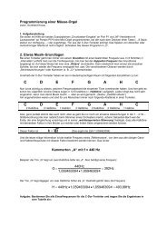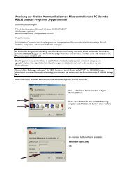
Clock Synchronous Serial I/O Mode - von Gunthard Kraus
Clock Synchronous Serial I/O Mode - von Gunthard Kraus
Clock Synchronous Serial I/O Mode - von Gunthard Kraus

You also want an ePaper? Increase the reach of your titles
YUMPU automatically turns print PDFs into web optimized ePapers that Google loves.
APPLICATION NOTE<br />
R8C/10, R8C/11, R8C/12, R8C/13 Group<br />
<strong>Serial</strong> I/O Operation (<strong>Clock</strong> <strong>Synchronous</strong> <strong>Serial</strong> I/O <strong>Mode</strong>)<br />
1. Abstract<br />
This application note describes a program that sends and receives 10 bytes successively by using clock<br />
synchronous serial I/O mode.<br />
2. Introduction<br />
The explanation of this issue is applied to the following condition:<br />
Microcomputer<br />
: R8C/10, R8C/11, R8C/12, R8C/13 Group<br />
Main clock input oscillation frequency :16MHz<br />
This program can also be used when operating other microcomputers within the R8C/Tiny, provided they<br />
have the same SFR (Special Function Registers) as the R8C/11 microcomputers. However, some functions<br />
may have been modified.<br />
Refer to the Hardware Manual for details. Use functions covered in this Application Note only after careful<br />
evaluation.<br />
3. Contents<br />
Specifications for transmit/receive operations are described below. The transfer format is shown in Figure 1.<br />
(1) <strong>Clock</strong> synchronous serial I/O mode of UART0 is used. The transfer clock is an internal clock, 8<br />
µs-cycle, LSB-first, with successive receive mode enabled. Data is transmitted on the falling edge of<br />
the transfer clock and received on the rising edge, with the TXD pin configured as CMOS output.<br />
(2) Ten bytes of data are transmitted/received successively, one byte every 250 µs. For transmit<br />
operation, the data in the variable trn_buf[serial_cnt] is transmitted. The received data is stored in<br />
the variable rcv_buf[serial_cnt–1]. The timer X is used to measure 250 µs.<br />
(3) When transmission of 10 bytes of data has finished, 10 bytes of data are transmitted/received 1 ms<br />
later again. That way, 10 bytes of data are transmitted/received repeatedly every 3.5 ms.<br />
Note that for reasons of SFR bit assignments, operation in this sample program may involve manipulating<br />
some bits whose functions are unused. Make sure the values of these bits are set according to the working<br />
condition in the user system.<br />
REJ05B0452-0110Z/Rev.1.10 August 2004 Page 1 of 11
R8C/10, R8C/11, R8C/12, R8C/13 Group<br />
<strong>Serial</strong> I/O Operation (<strong>Clock</strong> <strong>Synchronous</strong> <strong>Serial</strong> I/O <strong>Mode</strong>)<br />
3.5ms<br />
250µs 250µs<br />
1ms<br />
CLK0<br />
1 2 3 4 10 1<br />
TXD0<br />
1 2 3 4 10 1<br />
RXD0<br />
1 2 3 4 10 1<br />
8µs<br />
CLK0<br />
TxD0 D0 D1 D2<br />
D3 D4 D5 D6 D7<br />
RxD0<br />
D0<br />
D1<br />
D2<br />
D3 D4 D5 D6 D7<br />
Figure 1. Transmit Format<br />
3.1 Pins Used<br />
Table 1. List of Pins Used and Their Functions<br />
Pin name I/O Function<br />
P14/TxD0 Output <strong>Serial</strong> data output<br />
P15/RxD0 Input <strong>Serial</strong> data input<br />
P16/CLK0 Output Transfer clock output<br />
3.2 Memory Usage<br />
Table 2. Memory Usage<br />
Memory Usage Size Remarks<br />
ROM 167 bytes In only the main.c module<br />
RAM 21 bytes In only the main.c module<br />
Maximum user stack used 6 bytes sfr_init function: 3 bytes<br />
Cs_sral function: 3 bytes<br />
Maximum interrupt stack used 0 byte Unused<br />
The size of the used memory differs with the C compiler version and compile options. The above applies to the conditions<br />
given below.<br />
• C compiler: M3T-NC30WA V.5.20 Release 1<br />
• Compile option: -g -O -finfo Note - R8C<br />
Note: Unusable in the R8C/Tiny-only free version.<br />
Table 4. RAM Usage and Definition<br />
Symbol Type Size Content<br />
serial_cnt unsigned char 1 byte Transmit/receive data counter<br />
rcv_buf[10] unsigned char 10 bytes Receive buffer<br />
trn_buf[10] unsigned char 10 bytes Transmit buffer<br />
REJ05B0452-0110Z/Rev.1.10 August 2004 Page 2 of 11
R8C/10, R8C/11, R8C/12, R8C/13 Group<br />
<strong>Serial</strong> I/O Operation (<strong>Clock</strong> <strong>Synchronous</strong> <strong>Serial</strong> I/O <strong>Mode</strong>)<br />
4. Flow Chart<br />
4.1 Initial Operation and Main Loop<br />
main<br />
asm("FCLR I")<br />
prc0 = 1<br />
cm13 = 1<br />
cm15 = 1<br />
cm05 = 0<br />
cm16 = 0<br />
cm17 = 0<br />
cm06 = 0<br />
; Interrupt disabled<br />
; System clock control register protect cancellation<br />
; XIN-XOUT pin<br />
; XIN-XOUT drive capability : HIGH<br />
; Main clock : oscillation<br />
; No division mode<br />
; Main clock division CM16, CM17 enabled<br />
asm("nop")<br />
asm("nop")<br />
asm("nop")<br />
; Wait for stability (Main clock)<br />
asm("nop")<br />
ocd2 = 0<br />
prc0 = 0<br />
SFR INITIAL SETTING<br />
sfr_init<br />
; Select main clock<br />
; System clock control register protect<br />
; SFR initial setting (port initial setting, timer setting)<br />
Main period process<br />
No<br />
; Timer X wait for request (250µs)<br />
Yes<br />
ir_txic = 0<br />
; Timer X request flag clear<br />
SERIAL TRANSMIT/RECEIVE<br />
Cs_sral<br />
; <strong>Serial</strong> transmit/receive process (clock synchronized)<br />
REJ05B0452-0110Z/Rev.1.10 August 2004 Page 3 of 11
R8C/10, R8C/11, R8C/12, R8C/13 Group<br />
<strong>Serial</strong> I/O Operation (<strong>Clock</strong> <strong>Synchronous</strong> <strong>Serial</strong> I/O <strong>Mode</strong>)<br />
4.2 SFR Initial Setting<br />
sfr_init<br />
p1 = p1 | 0x50<br />
pd1 = pd1 | 0x50<br />
pd1 = pd1 & 0xdf<br />
txck0 = 1<br />
txck1 = 0<br />
prex = 50-1<br />
tx = 10-1<br />
txmr = 0x00<br />
txs = 1<br />
u0mr = 0x01<br />
u0c0 = 0x01<br />
u0rrm = 0<br />
u0brg = 8-1<br />
re_u0c1 = 1<br />
; Port P14,P16 initial setting<br />
; Port P14,P16 direction bit initial setting<br />
; Port P15 direction bit initial setting<br />
; Timer X count source : f8<br />
; Prescaler X = 50<br />
; Timer X = 10<br />
; Timer X : timer mode<br />
; Timer X count start<br />
; <strong>Clock</strong> synchronous serial I/O mode<br />
Internal clock<br />
; BRG count source :f8sio<br />
TXD0: CMOS output<br />
Transmit data is output at falling edge of transfer clock<br />
and receive data is input at rising edge<br />
LSB first<br />
; Continuous receive mode disabled<br />
; Count source: Divided-by 8<br />
; Reception enabled<br />
return<br />
REJ05B0452-0110Z/Rev.1.10 August 2004 Page 4 of 11
R8C/10, R8C/11, R8C/12, R8C/13 Group<br />
<strong>Serial</strong> I/O Operation (<strong>Clock</strong> <strong>Synchronous</strong> <strong>Serial</strong> I/O <strong>Mode</strong>)<br />
4.3 <strong>Serial</strong> I/O (<strong>Clock</strong> <strong>Synchronous</strong> <strong>Serial</strong> I/O) Process<br />
Cs_sral<br />
serial_cnt >= 1<br />
No<br />
; Receiving serial communication data now<br />
Yes<br />
serial_cnt
R8C/10, R8C/11, R8C/12, R8C/13 Group<br />
<strong>Serial</strong> I/O Operation (<strong>Clock</strong> <strong>Synchronous</strong> <strong>Serial</strong> I/O <strong>Mode</strong>)<br />
5. Programming Code<br />
/************************************************************************************<br />
* *<br />
* File Name : main.c *<br />
* Contents : Main program of the sample program No.9 R8C/11 Group *<br />
* Copyright(C)2003, Renesas Technology Corp. *<br />
* Copyright(C)2003, Renesas Solutions Corp. *<br />
* All rights reserved. *<br />
* Version : 1.10 *<br />
* note : 0.01 : First version *<br />
* : 1.10(2004.08.02): Comment is revised *<br />
************************************************************************************/<br />
#include "sfr_r811.h" /* Definition of the R8C/11 SFR */<br />
/* Definition of RAM area */<br />
unsigned char serial_cnt; /* <strong>Serial</strong> I/O counter */<br />
unsigned char rcv_buf[10]; /* Reception buffer */<br />
unsigned char trn_buf[10]; /* Transmission buffer */<br />
/* Declaration of function prototype */<br />
void sfr_init(void); /* Initial setting of SFR registers */<br />
void Cs_sral(void); /* <strong>Clock</strong> synchronous serial I/O sub routine */<br />
main() {<br />
asm("FCLR I"); /* Interrupt disable */<br />
/*-----------------------------------------------<br />
-Change on-chip oscillator clock to Main clock -<br />
-------------------------------------------------*/<br />
prc0 = 1; /* Protect off */<br />
cm13 = 1; /* Xin Xout */<br />
cm15 = 1; /* XCIN-XCOUT drive capacity select bit : HIGH */<br />
cm05 = 0; /* Xin on */<br />
cm16 = 0; /* Main clock = No division mode */<br />
cm17 = 0;<br />
cm06 = 0; /* CM16 and CM17 enable */<br />
asm("nop"); /* Waiting for stable of oscillation */<br />
asm("nop");<br />
asm("nop");<br />
asm("nop");<br />
ocd2 = 0; /* Main clock change */<br />
prc0 = 0; /* Protect on */<br />
/*-----------------------------------<br />
- Initialize SFR -<br />
-----------------------------------*/<br />
sfr_init(); /* Initial setting of SFR registers */<br />
}<br />
/*-----------------------------------<br />
- Loop of main -<br />
-----------------------------------*/<br />
while(1){ /* Main processing */<br />
while(ir_txic == 0){} /* Main cycle 250us */<br />
ir_txic = 0;<br />
Cs_sral(); /* <strong>Clock</strong> synchronous serial I/O */<br />
}<br />
REJ05B0452-0110Z/Rev.1.10 August 2004 Page 6 of 11
R8C/10, R8C/11, R8C/12, R8C/13 Group<br />
<strong>Serial</strong> I/O Operation (<strong>Clock</strong> <strong>Synchronous</strong> <strong>Serial</strong> I/O <strong>Mode</strong>)<br />
/************************************************************************************<br />
Name: sfr_init<br />
Parameters: None<br />
Returns: None<br />
Description: Initial setting of SFR registers<br />
************************************************************************************/<br />
void sfr_init(void){<br />
/* Setting port registers */<br />
p1 = p1 | 0x50; /* TxD0, CLK0 port off */<br />
/* Setting port direction registers */<br />
pd1 = pd1 | 0x50; /* TxD0, CLK0 port direction = output */<br />
pd1 = pd1 & 0xdf; /* RxD0 port direction = input */<br />
txck0 = 1; /* Timer X count source = f8 */<br />
txck1 = 0;<br />
/* 16MHz* 1/8 * 50 * 10 = 250us */<br />
prex = 50-1; /* Setting Prescaler X register */<br />
tx = 10-1; /* Setting timer X register */<br />
txmr = 0x00; /* Timer X : timer mode */<br />
txs = 1; /* Timer X count start flag = start */<br />
}<br />
/* <strong>Clock</strong> synchronous serial I/O setting */<br />
u0mr = 0x01; /* Set clock synchronous serial I/O mode */<br />
/* Internal <strong>Clock</strong> */<br />
u0c0 = 0x01; /* f8 is selected */<br />
/* Data present in transmit register */<br />
/* (during transmission) */<br />
/* TXD0 pin is CMOS output */<br />
/* Transmit data is output at falling edge of */<br />
/* transfer clock and receive data */<br />
/* is input at rising edge */<br />
/* LSB first */<br />
u0rrm = 0; /* Continuous receive mode disabled */<br />
u0brg = 8-1; /* Set baud rate:1 clock 8us */<br />
re_u0c1 = 1; /* Reception enabled */<br />
REJ05B0452-0110Z/Rev.1.10 August 2004 Page 7 of 11
R8C/10, R8C/11, R8C/12, R8C/13 Group<br />
<strong>Serial</strong> I/O Operation (<strong>Clock</strong> <strong>Synchronous</strong> <strong>Serial</strong> I/O <strong>Mode</strong>)<br />
/************************************************************************************<br />
Name: Cs_sral<br />
Parameters: None<br />
Returns: None<br />
Description: <strong>Clock</strong> synchronous sereial I/O<br />
************************************************************************************/<br />
void Cs_sral(void){<br />
unsigned short rcv_work;<br />
/* Store a receive data to receive data buffer from receive register */<br />
if ((serial_cnt >= 1) && (serial_cnt < 10 + 1)){<br />
rcv_work = u0rb;<br />
rcv_buf[serial_cnt - 1] = (unsigned char)rcv_work; /* Get Reception data */<br />
}<br />
/* Set a send data to send register from send data buffer */<br />
if (serial_cnt < 10){<br />
u0tbl = trn_buf[serial_cnt]; /* Set send data */<br />
te_u0c1 = 1; /* Transmission enabled */<br />
}<br />
}<br />
/* Set next send data point */<br />
serial_cnt++; /* Increment counter */<br />
if (serial_cnt == 10 + 4){<br />
serial_cnt = 0; /* Clear counter */<br />
}<br />
REJ05B0452-0110Z/Rev.1.10 August 2004 Page 8 of 11
R8C/10, R8C/11, R8C/12, R8C/13 Group<br />
<strong>Serial</strong> I/O Operation (<strong>Clock</strong> <strong>Synchronous</strong> <strong>Serial</strong> I/O <strong>Mode</strong>)<br />
6. Reference<br />
Renesas Technology Corporation Home Page<br />
http://www.renesas.com/<br />
E-mail Support<br />
E-mail: support_apl@renesas.com<br />
Hardware Manual<br />
R8C/10 Group Hardware Manual<br />
R8C/11 Group Hardware Manual<br />
R8C/12 Group Hardware Manual<br />
R8C/13 Group Hardware Manual<br />
(Use the latest version on the home page: http://www.renesas.com)<br />
REJ05B0452-0110Z/Rev.1.10 August 2004 Page 9 of 11
R8C/10, R8C/11, R8C/12, R8C/13 Group<br />
<strong>Serial</strong> I/O Operation (<strong>Clock</strong> <strong>Synchronous</strong> <strong>Serial</strong> I/O <strong>Mode</strong>)<br />
REVISION HISTORY<br />
Rev. Date<br />
Page<br />
1.10 2004.08.02 - First edition issued<br />
Description<br />
Summary<br />
REJ05B0452-0110Z/Rev.1.10 August 2004 Page 10 of 11
R8C/10, R8C/11, R8C/12, R8C/13 Group<br />
<strong>Serial</strong> I/O Operation (<strong>Clock</strong> <strong>Synchronous</strong> <strong>Serial</strong> I/O <strong>Mode</strong>)<br />
Keep safety first in your circuit designs!<br />
Keep safety first in your circuit designs!<br />
Notes regarding these materials<br />
1. Renesas Technology Corporation puts the maximum effort into making semiconductor products<br />
better and more reliable, but there is always the possibility that trouble may occur with them. Trouble<br />
with semiconductors may lead to personal injury, fire or property damage.<br />
Remember to give due consideration to safety when making your circuit designs, with appropriate<br />
measures such as (i) placement of substitutive, auxiliary circuits, (ii) use of nonflammable material or<br />
(iii) prevention against any malfunction or mishap.<br />
Notes regarding these materials<br />
1. These materials are intended as a reference to assist our customers in the selection of the Renesas<br />
Technology Corporation product best suited to the customer's application; they do not convey any<br />
license under any intellectual property rights, or any other rights, belonging to Renesas Technology<br />
Corporation or a third party.<br />
2. Renesas Technology Corporation assumes no responsibility for any damage, or infringement of any<br />
third-party's rights, originating in the use of any product data, diagrams, charts, programs,<br />
algorithms, or circuit application examples contained in these materials.<br />
3. All information contained in these materials, including product data, diagrams, charts, programs and<br />
algorithms represents information on products at the time of publication of these materials, and are<br />
subject to change by Renesas Technology Corporation without notice due to product improvements<br />
or other reasons. It is therefore recommended that customers contact Renesas Technology<br />
Corporation or an authorized Renesas Technology Corporation product distributor for the latest<br />
product information before purchasing a product listed herein.<br />
The information described here may contain technical inaccuracies or typographical errors.<br />
Renesas Technology Corporation assumes no responsibility for any damage, liability, or other loss<br />
rising from these inaccuracies or errors.<br />
Please also pay attention to information published by Renesas Technology Corporation by various<br />
means, including the Renesas Technology Corporation Semiconductor home page<br />
(http://www.renesas.com).<br />
4. When using any or all of the information contained in these materials, including product data,<br />
diagrams, charts, programs, and algorithms, please be sure to evaluate all information as a total<br />
system before making a final decision on the applicability of the information and products. Renesas<br />
Technology Corporation assumes no responsibility for any damage, liability or other loss resulting<br />
from the information contained herein.<br />
5. Renesas Technology Corporation semiconductors are not designed or manufactured for use in a<br />
device or system that is used under circumstances in which human life is potentially at stake.<br />
Please contact Renesas Technology Corporation or an authorized Renesas Technology Corporation<br />
product distributor when considering the use of a product contained herein for any specific<br />
purposes, such as apparatus or systems for transportation, vehicular, medical, aerospace, nuclear,<br />
or undersea repeater use.<br />
6. The prior written approval of Renesas Technology Corporation is necessary to reprint or reproduce<br />
in whole or in part these materials.<br />
7. If these products or technologies are subject to the Japanese export control restrictions, they must<br />
be exported under a license from the Japanese government and cannot be imported into a country<br />
other than the approved destination.<br />
Any diversion or reexport contrary to the export control laws and regulations of Japan and/or the<br />
country of destination is prohibited.<br />
8. Please contact Renesas Technology Corporation for further details on these materials or the<br />
products contained therein.<br />
REJ05B0452-0110Z/Rev.1.10 August 2004 Page 11 of 11