
You also want an ePaper? Increase the reach of your titles
YUMPU automatically turns print PDFs into web optimized ePapers that Google loves.
<strong>Quantum</strong> <strong>Dot</strong> <strong>Lasers</strong><br />
Lecture in Modern Optics by Björn Agnarsson<br />
Most of this text is taken from the book “<strong>Quantum</strong> <strong>Dot</strong> Heterostructures” by Dieter<br />
Bimberg, Marius Grundmann and Nikolai N. Ledentsov.<br />
Fabrication of quantum dots<br />
<strong>Quantum</strong> dots (QD) can be made using a variety of methods but for real applications<br />
mainly three methods are used:<br />
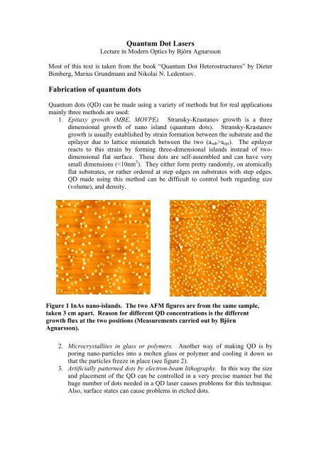
1. Epitaxy growth (MBE, MOVPE). Stransky-Krastanov growth is a three<br />
dimensional growth of nano island (quantum dots). Stransky-Krastanov<br />
growth is usually established by strain formation between the substrate and the<br />
epilayer due to lattice mismatch between the two (a sub >a epi ). The epilayer<br />
reacts to this strain by forming three-dimensional islands instead of twodimensional<br />
flat surface. These dots are self-assembled and can have very<br />
small dimensions (
Figure 2 Schematic representation of different approaches to fabrication of<br />
nanostructures: (a) microcrystallites in glass, (b) artificial patterning of thin film<br />
structures, (c) self-organized growth of nanostructures (Betul Arda, Huizi Diwu.<br />
Department of Electrical and Computer Engineering University of Rochester)<br />
Key-issues in fabrication:<br />
1. The QD needs to be small in order for the carriers to be as three dimensionally<br />
confined as possible in space (so we get energy delta functions). The threedimensional<br />
confinement potential needs to be significantly high in order for<br />
the carriers (electrons/holes) not to be thermally excited out of the QD. QDs<br />
need to be operational at and above room, meaning that this potential needs to<br />
be substantially larger than kT room =25meV.<br />
2. We need many QDs.<br />
3. QDs need to be as homogeneous as possible; otherwise we will get a spread in<br />
our discrete energy levels (see figure below).<br />
Figure 3
Physics<br />
Electrons/holes can be confined in all three dimensions in a dot or a quantum box.<br />
The situation is analogues to that of a hydrogen atom meaning that only discrete<br />
energy levels are possible. The density of states if given by.<br />
So we end up with discrete energy levels:<br />
ρ 0D<br />
= 2δ(E)<br />
E − E C<br />
= E n,m,p<br />
= π 2 h 2 ⎛ n 2<br />
2m * 2<br />
L + m 2<br />
⎜ 2<br />
⎝ x<br />
L y<br />
+ p2<br />
L z<br />
2<br />
⎞<br />
⎟<br />
⎠<br />
Figure 4 Quantization of density of states: (a) bulk (b) quantum well (c)<br />
quantum wire (d) QD (Betul Arda, Huizi Diwu. Department of Electrical and<br />
Computer Engineering University of Rochester)<br />
QD-lasers<br />
In principle, QD lasers can be treated in a similar way as quantum well (QW) lasers<br />
and the laser structure is fabricated in a similar way, the only difference being that the<br />
optically active medium consists of QDs instead of QWs. The figure below shows a<br />
simple laser structure, consisting of an active layer embedded in a waveguide,<br />
surrounded by layers of lower refractive index to ensure light confinement. The active<br />
material consists of quantum wells or quantum dots where the bandgap is lower than<br />
that of the waveguide material.
Waveguide with<br />
active layer<br />
Figure 5<br />
The active layer (QD or QW) is embedded in an optical waveguide (material with<br />
refractive index smaller than that of the active layer).<br />
Wavelength of the emitted light is determined by the energy levels of the QD rather<br />
than the band-gap energy of the dot material. Therefore, the emission wavelength can<br />
be tuned by changing the average size of the dots.<br />
Because the band-gap of the QD material is lower than the band gap of the<br />
surrounding medium we ensure carrier confinement. A structure like this, were<br />
carrier confinement is realized separately from the confinement of the optical wave, is<br />
called a separate-confinement heterostructure (SCH).<br />
Figure 6 An ideal QD laser consists of a 3D-array of dots with equal size and<br />
shape, ssurrounded by a higher band-gap material (confines the injected<br />
carriers). The barrier material forms an optical waveguide with lower and<br />
upper cladding layers (n-doped and p-doped AlGaAs in this case). (Betul Arda,<br />
Huizi Diwu. Department of Electrical and Computer Engineering University of<br />
Rochester)
Optical Confinement factor<br />
For a QD array, the optical confinement factor, G, is on the order of total dot volume<br />
to total waveguide volume. It can be split into in-plane and vertical components. For<br />
consistency with a similar treatment for QW lasers, it should be pointed out that this<br />
notation is most appropriate for vertical-cavity quantum dot lasers where the light<br />
propagation is perpendicular to the active layer:<br />
Where<br />
Γ = Γ xy<br />
Γ z<br />
Γ xy<br />
= N D A D<br />
A<br />
= ξ<br />
Where N D is the number of QD, A D is the average in-plane size of the QD and A is the<br />
xy-area of the waveguide. The factor ξ is called the area coverage of QD.<br />
The vertical component of the confinement factor is given by the ratio of the light<br />
intensity in the active layer (QD), averaged over area A, to the total light intensity in<br />
the whole heterostructure. This ratio characterizes the overlap between the QD and<br />
the optical mode.<br />
Γ z<br />
= 1 A<br />
∫ E(z) 2 dz / ∫ E(z) 2<br />
dz<br />
QD<br />
Example:<br />
For N D /A=4 x 10 10 QD/cm 2 and volume of QD equal to 7*7*2 nm 3 . We get ξ= 0.02.<br />
For a 150nm thick cavity a typical vertical optical confinement factor is 0.007. Hence<br />
the total optical confinement factor is 1.4e-4<br />
It is worth noticing that since:<br />
whole<br />
Γ xy<br />
∝ N D<br />
by increasing the number of dots (or more precisely by increasing the area coverage<br />
of QD, ξ) we get an increase in the total optical confinement factor. In a similar way<br />
since G z is proportional to the thickness of the active layer, by increasing the number<br />
of QD layers in the active layer (increasing the number of active layers) an increase in<br />
the vertical optical confinement factor is achieved. Both these cases are illustrated in<br />
the figures below and both contribute to the total optical confinement factor.
Figure 7<br />
Gain and threshold<br />
As always, in order to achieve lasing we need population inversion and stimulated<br />
emission together with some sort of feedback provided usually by reflection by<br />
mirrors. The population inversion is obtained by electrically pumping the system with<br />
carriers (holes and electrons). In a simple 2-fold degenerate energy level system, this<br />
is achieved when enough current is pumped into the system in order to invert the<br />
ground-state population level. That is to say, on average there is more than one<br />
electron-hole residing in the QD conduction-band state and more than one hole<br />
residing in the QD valence-band state.<br />
At a certain threshold current density (j th ), the lasing starts and by increasing the<br />
current above that threshold we increase the output power linearly with increasing<br />
current. The condition for lasing can be written as:<br />
g mod<br />
( j th<br />
) = Γg material<br />
( j th<br />
) = α tot<br />
Where g mod is the modal gain of the system and a tot is the total loss in the system<br />
consisting of internal losses in the active layer (a i ), losses in the waveguide (a c ) and<br />
losses at the reflectors (a mirrors ).<br />
So modal gain is given by:<br />
α tot<br />
=Γα i<br />
+ (1 −Γ)α c<br />
+ 1<br />
2L ln( 1<br />
R 1<br />
R 2<br />
)<br />
g mod<br />
( j) = Γg material<br />
( j) −α tot<br />
Assuming that the we have a Gaussian distribution in QD volume size (P g ), and that<br />
spectral width of this distribution is much bigger than the width of the Lorentzian<br />
describing the intra-band relaxation times, the material gain g mat of a QD ensemble<br />
can be calculated using the following formula:<br />
g mat<br />
(E) = C g<br />
P(E) [ f c<br />
(E, E Fc<br />
) − f v<br />
(E, E Fv<br />
)]<br />
Where C is a constant and P g is the Gaussian distribution and f is the Fermi<br />
distribution of the carriers. If one further assumes that the all the injected carriers are
captured by QD and that overall charge neutrality exists (i.e f v =1-f c and f c -f v =2f c -1),<br />
the total number (N) of carriers (electrons and holes) is:<br />
N = 2 f c<br />
N D<br />
and these carriers are assumed to be equally distributed amongst all the QD. So we<br />
end up with a material gain:<br />
g mat<br />
(E) = N − N D<br />
N D<br />
C g<br />
P(E)<br />
If we take a closer look at this expression for the material gain we see that it increases<br />
linearly with increasing number of carriers, N, from –C g P(E) (when the QD excited<br />
state has no carriers) to C g P(E) (when all QD excited states are filled with 2 electrons,<br />
N max =2N D ).<br />
Figure 8<br />
For typical values of C and P(E) we obtain a maximum saturation value in the<br />
material gain in the order of 1e5 cm -1 , which is huge! However, due to the optical<br />
confinement factor one ends up with a much smaller modal gain (g mod =Γg mat ).<br />
We also see that the shape of the gain function depends on the Gaussian distribution<br />
function P(E). This means that the shape of the gain function depends strongly on the<br />
uniformity of the QD volume size and shape. The more homogenous the system is,<br />
the sharper and higher the gain function is.
Figure 9 Calculated material gain spectra for In 0.53 Ga 0.47 As/InP quantum box,<br />
wire, well and bulk at T=300 K. Electron density at 3x10 18 cm -3 (After Asada el<br />
al., 1986). Notice the height of the QD peak and its width. (<strong>Quantum</strong> <strong>Dot</strong><br />
Heterostructures by Dieter Bimberg, Marius Grundmann and Nikolai N.<br />
Ledentso)<br />
Example:<br />
For 7*7*2 nm 3 QD with ζ=0.02 (corresponding to 4x10 -10 QD/cm 2 ), Γ z =7x10 -3 for<br />
150nm waveguide and saturation material gain g mat =1e5, we only get:<br />
To prevent gain saturation<br />
sat<br />
g mod<br />
sat<br />
= Γg mat<br />
sat<br />
= Γ xy<br />
Γ z<br />
g mat<br />
sat<br />
= ξΓ z<br />
g mat<br />
=14 cm -1<br />
In order to increase the gain saturation limit of given QD ensemble, the following<br />
steps could be used:<br />
1. Increase the modal gain by stacking layers of QD within the active layer<br />
2. Increase the number of QD (N D ) in each sheet of QD in the active layer<br />
3. Decrease the mirror loss by high reflection coatings or many mirrors. In<br />
VCSEL we usually have small cavity length L. According to the<br />
expression for losses in mirrors this would mean larger loss the smaller the<br />
cavity. This could be compensated by having R 1 and R 2 high, either by<br />
using high reflective coatings or by using many sets of mirrors (20 mirrors<br />
in VCSEL give about 99% reflection).
In order to have lasing, the carrier density at threshold, N th , has to be at least:<br />
⎛<br />
N th<br />
= N D ⎜ 1+ 1<br />
⎝ ξ<br />
2πσ E<br />
α tot<br />
Γ z<br />
C g<br />
⎞<br />
⎟<br />
⎠<br />
The maximum threshold current density is:<br />
N th max = 2N D<br />
So the minimum area dot coverage has to be:<br />
ξ min<br />
=<br />
2πσ Eα tot<br />
Γ z<br />
C g<br />
The relationship between carrier density, N, and injection current, j, is non-trivial but<br />
a simplified version, obtained using conventional rate equation models, gives:<br />
j = 5 8<br />
e ⎛<br />
ξ⎜<br />
A D<br />
τ D ⎝<br />
N ⎞<br />
⎟<br />
N D ⎠<br />
2<br />
Using the above relation for threshold density of states, N th , we obtain the following<br />
relation for the threshold current, j th :<br />
j th<br />
= 5 8<br />
e ⎛<br />
ξ 1+ ξ ⎞<br />
min<br />
⎜ ⎟<br />
A D<br />
τ D ⎝ ξ ⎠<br />
2<br />
Figure 10 Threshold current density as a function of dot area coverage<br />
For ξ < ξ min the current density goes to infinity and we will not get any lasing.
Example:<br />
For a tot equal to 10 cm -1 and ξ min equal to 0.013 we get a threshold current of 10A/cm 2<br />
By increasing the number of active layers we obtain a decrease in threshold current:<br />
J th = 90 A/cm 2 for 10 layers of In 0.5 Ga 0.5 As/GaAs<br />
J th = 62 A/cm 2 for 3 layers of In 0.5 Ga 0.5 As/Al 0.15 Ga 0.75 As<br />
J th = 40 A/cm 2 for 3 layers of InAs/GaAs<br />
Figure 11<br />
Advantages and complications with QD lasers<br />
Problems:<br />
• Wavefunction is not zero at potential barriers and hence penetrate into it<br />
• m* can be discontinuous, meaning that masses in wells and barriers differ<br />
• Non-parabolicity of E-k which means that the mass changes with energy<br />
• Multiple band in valance band (heavy and light holes)<br />
• Fabrication process can be complicated leading to non-homogenous in size<br />
and shape leading to the broadening of the gain spectrum (see figure 3).<br />
• High material gain but low optical confinement factor leads to low modal gain<br />
• Barriers are finite, not infinite, meaning that there is a carrier leakage out of<br />
the QD<br />
• Strained wells might lead to shift in wavelength due to the existence of light<br />
and heavy holes in the valance band.
Advantages:<br />
• Adjustable wavelengths since energy levels rather than band-gap determine<br />
the wavelength<br />
• Higher material gain for QD than for QW and quantum wires (QD gain is 10x<br />
more than QW gain)<br />
• Material gain curve is narrower than for QW and quantum wires.<br />
• Small volume<br />
o Low power needed<br />
o High frequency operation possible<br />
o Small linewidth of emission peak<br />
o Low threshold current need compared to QW and quantum wires.<br />
• Superior temperature stability compared to QW<br />
• Suppressed diffusion of carriers compared to QW<br />
Figure 12 Temperature dependence of<br />
light-current characteristics (Fujitsu<br />
Temperature Independent QD laser<br />
2004)<br />
Figure 13 Modulation waveform at<br />
10Bbps at 20°C and 70 °C with no<br />
current characteristics (Fujitsu<br />
Temperature Independent QD laser<br />
2004).<br />
Figure 14 Comparison betweeen QD and QW laser. (Betul Arda, Huizi Diwu.<br />
Department of Electrical and Computer Engineering University of Rochester)