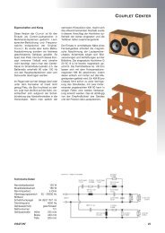
PDF download
PDF download
PDF download

You also want an ePaper? Increase the reach of your titles
YUMPU automatically turns print PDFs into web optimized ePapers that Google loves.
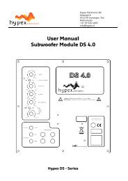
SMPS400A180<br />
SMPS400A400<br />
DISCLAIMER: This product is designed for use in sound reproduction equipment in<br />
conjunction with Hypex amplifier modules. No representations are made as to fitness for<br />
use in other applications. Except where noted otherwise any specifications given pertain to<br />
this subassembly only. Responsibility for verifying the performance, safety, reliability and<br />
compliance with legal standards of end products using this subassembly falls to the<br />
manufacturer of said end product.<br />
LIFE SUPPORT POLICY: Use of Hypex products in life support equipment or equipment whose<br />
failure can reasonably be expected to result in injury or death is not permitted except by<br />
explicit written consent from Hypex Electronics BV.<br />
Document PCB<br />
Description<br />
Date<br />
Revision Version<br />
R1 SMPS400V1 Initial Draft. Applicable to SMPS400/67/47/37 V1 26.02.2009<br />
R2 SMPS400V2 - /37 version deleted.<br />
03.04.2009<br />
- /47 output voltage increased from 47V to 49V.<br />
R3 SMPS400V3 - Changed output connector style for compatibility 04.05.2009<br />
reasons.<br />
- Current limiter further improved.<br />
- Transformer changed for better efficiency.<br />
- Audiophile performance improved.<br />
R4 SMPS400V4 TR3 moved for better fit.<br />
R5 SMPS400V4 - Auxiliary output voltage increased to 2 x 21V.<br />
05.06.2009<br />
- J3/J4 combined to a single 5-pin header to avoid wiring<br />
errors.<br />
R6 SMPS400V5 - Product names changed to indicate which amplifier 10.02.2010<br />
should be used with the SMPS400 (..A180, ..A400) .<br />
- J3/J4 combined to J5. Connection tables adjusted.<br />
- Trademark signs (UcD into UcD ® ) .<br />
- Several component changes in input and output stage.<br />
R7 SMPS400V6 - Output voltage reduced to comply to mains range. 03.03.2010<br />
R8 SMPS400V8 - Installation instruction added. 01.06.2010<br />
R9 SMPS400V8 - Output voltages corrected.<br />
20.07.2010<br />
- Output power data added.<br />
R10 SMPS400V8 - Power figures corrected.<br />
19.11.2010<br />
- Thermal cut-off threshold added.<br />
- Safety precautions extended.<br />
R11 SMPS400V9 - Output power figures corrected for 46V output variant. 20.01.2011<br />
- DC-error reset procedure changed.<br />
R12 SMPS400V9 - Auxiliary output voltage corrected.<br />
04.04.2011<br />
- DC-error input characteristics corrected.<br />
R13 SMPS400V9 - Spacers are not included in package text added.<br />
05.05.2011<br />
- J7 grounding connection added<br />
R14 SMPS400V9 - Idle losses corrected<br />
13.05.2011<br />
- Thermal performance data<br />
R15 SMPS400V9 - Correct auxiliary output voltage ambiguity 06.06.2011<br />
R16 SMPS400V9 - Connector references corrected in description table<br />
- Format changed<br />
05.06.2012<br />
R16 12