PDF download
PDF download
PDF download

Create successful ePaper yourself
Turn your PDF publications into a flip-book with our unique Google optimized e-Paper software.
Kattegat 8<br />
9723 JP Groningen, The Netherlands<br />
+31 50 526 4993<br />
sales@hypex.nl<br />
www.hypex.nl<br />
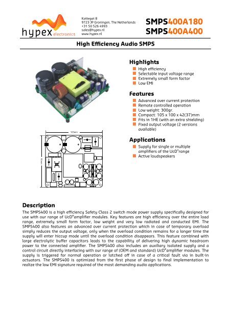
SMPS400A180<br />
SMPS400A400<br />
High Efficiency Audio SMPS<br />
Highlights<br />
High efficiency<br />
Selectable input voltage range<br />
Extremely small form factor<br />
Low EMI<br />
Features<br />
Advanced over current protection<br />
Remote controlled operation<br />
Low weight: 300gr.<br />
Compact: 105 x 100 x 42(37)mm<br />
Fits in 1HE (with an extra shielding)<br />
Fixed output voltage (2 versions<br />
available)<br />
Applications<br />
Supply for single or multiple<br />
amplifiers of the UcD ® range<br />
Active loudspeakers<br />
Description<br />
The SMPS400 is a high efficiency Safety Class 2 switch mode power supply specifically designed for<br />
use with our range of UcD ® amplifier modules. Key features are high efficiency over the entire load<br />
range, extremely small form factor, low weight and very low radiated and conducted EMI. The<br />
SMPS400 also features an advanced over current protection which in case of temporary overload<br />
simply reduces the output voltage, only when the overload condition remains for a longer time the<br />
supply will enter hiccup mode until the overload condition disappears. This feature combined with<br />
large electrolytic buffer capacitors leads to the capability of delivering high dynamic headroom<br />
power to the connected amplifier. The SMPS400 also includes an auxiliary isolated supply and a<br />
control circuit directly interfacing with our range of (OEM and standard) UcD ® amplifier modules. The<br />
supply is triggered for normal operation or latched off in case of a critical fault via in built-in<br />
actuators. The SMPS400 is optimized from the first phase of design to final implementation to<br />
realize the low EMI signature required of the most demanding audio applications.
SMPS400A180<br />
SMPS400A400<br />
Contents<br />
Contents ...........................................................................................................................................................2<br />
Principle of operation......................................................................................................................................2<br />
1 Safety precautions .................................................................................................................................3<br />
2 Instructions For Installation..................................................................................................................3<br />
3 Absolute maximum ratings...................................................................................................................4<br />
4 Recommended Operating Conditions...................................................................................................4<br />
5 General Performance data (All versions)..............................................................................................4<br />
6 General Performance data (SMPS400A400) ........................................................................................5<br />
7 General Performance data (SMPS400A180) ........................................................................................5<br />
8 Output Power Performance data (SMPS400A400)..............................................................................5<br />
9 Output Power (SMPS400A400) .............................................................................................................6<br />
10 Output Power (SMPS400A180).........................................................................................................6<br />
11 Connector Pinout................................................................................................................................7<br />
12 SMPS Standby Input Characteristics................................................................................................8<br />
13 Amplifier Standby Input Characteristics .........................................................................................8<br />
14 Unregulated Auxiliary Output Characteristics SMPS400A400 .....................................................9<br />
15 Unregulated Auxiliary Output Characteristics SMPS400A180 .....................................................9<br />
16 Output Voltage Characteristics SMPS400A400..............................................................................9<br />
17 Output Voltage Characteristics SMPS400A180..............................................................................9<br />
18 Output Grounds Characteristics.......................................................................................................9<br />
19 DC Error Input Characteristics ..........................................................................................................9<br />
20 Auto Amplifier Enable Characteristics ...........................................................................................10<br />
21 DC Error Input 1 & 2 Characteristics ..............................................................................................10<br />
22 Dimensions. Top view. .....................................................................................................................11<br />
23 Dimensions. Side view. ....................................................................................................................11<br />
Principle of operation<br />
Conventional Switch Mode Power Supplies are commonly unsuitable for audio purposes due to poor<br />
peak power capabilities and the inability to handle reversed currents generated by Class D amplifiers<br />
as a load. The Hypex SMPS400 achieves these things by using an advanced over current protection<br />
circuit, a highly efficient 2 quadrant DC/DC converter which is capable of handling reversed currents<br />
and has a peak power handling of many times its rated power.<br />
R16 2
1 Safety precautions<br />
SMPS400A180<br />
SMPS400A400<br />
The SMPS400 operates at mains voltage and carries hazardous voltages at<br />
accessible parts. These parts may never be exposed to inadvertent touch.<br />
Observe extreme care during installation and never touch any part of the<br />
unit while it is connected to the mains. Disconnect the unit from the mains<br />
and allow all capacitors to discharge for 10 minutes before handling it.<br />
This product has no serviceable parts other than the on-board fuse. Replace the fuse only with the<br />
same type and rating (250V T5AL).<br />
This is a Safety Class 2 device. It is very<br />
important to maintain a 6mm<br />
clearance with all possible conducting<br />
parts (housing etc.) and cables. All<br />
parts enclosed by the dotted line below<br />
carry hazardous voltages. This includes<br />
parts on the top and the bottom of the<br />
board. When the SMPS400 is mounted<br />
in a tight space there needs to be at<br />
least 6mm clearance or a layer of<br />
insulation with a minimum thickness<br />
of 0.5mm between the top of the<br />
transformer and the housing. Only use<br />
insulated spacers in the dotted area.<br />
The fourth hole should a conductive<br />
spacer to improve EMI preformance.<br />
Standard the SMPS400 is supplied with<br />
10mm spacers to mount the SMPS<br />
onto the chassis. This creates the<br />
mandatory 6mm clearance from the<br />
bottom side of the PCB to the chassis without the need for additional insulating material. However, If<br />
the enclosure is limited in height, for instance a 1HE 19” enclosure, one shall need to use smaller<br />
spacers and provide a layer of insulation both above and below the SMPS with a minimum thickness<br />
of 0.5mm in order to comply with the Class 2 Safety Directive. If these measures are taken into<br />
account, the maximum overall height can be reduced to 37mm.<br />
2 Instructions For Installation<br />
Warning: To reduce the risk of fire or electric shock, do not expose this apparatus to rain or<br />
moisture.<br />
Warning: Disconnect the unit from the mains and allow all capacitors to discharge for 10 minutes<br />
before handling it.<br />
This symbol indicates the presence of hazardous voltages at accessible conductive terminals<br />
on the board. Parts that are not highlighted in red (picture above) may carry voltages in<br />
excess of 140VDC!<br />
1. Read these instructions.<br />
2. Keep these instructions.<br />
3. Heed all warnings.<br />
4. Follow all instructions.<br />
R16 3
SMPS400A180<br />
SMPS400A400<br />
5. Do not use this apparatus near water.<br />
6. Protect the power cord from being walked on or pinched particularly at plugs, convenience<br />
receptacles, and the point where they exit from the application.<br />
7. Only use attachments/accessories specified or approved by the manufacturer.<br />
8. Unplug this apparatus during lightning storms or when unused for long periods of time.<br />
9. Refer all servicing to qualified service personnel. Servicing is required when the apparatus has<br />
been damaged in any way, liquid has been spilled or objects have fallen into the apparatus, the<br />
apparatus has been exposed to rain or moisture, does not operate normally or has been dropped.<br />
10. This product is to be used with Hypex amplifier modules only.<br />
11. Only the ready-made cable sets provided by Hypex may be used for external wiring of the<br />
SMPS400.<br />
12. Don’t run any cables across the top or the bottom of the SMPS400. Apply fixtures to cables to<br />
ensure that this is not compromised.<br />
13. Observe a minimum distance of 6mm maintain clearance with all possible conducting parts<br />
(housing etc.). All parts enclosed by the dotted line below carry hazardous voltages. This includes<br />
parts on the top and the bottom of the board. When the SMPS400 is mounted in a tight space there<br />
needs to be at least 6mm clearance or a layer of insulation with a minimum thickness of 0.5mm<br />
between the top of the transformer and the housing.<br />
14. Natural convection should not be impeded by covering the SMPS400 (apart from the end<br />
applications housing).<br />
3 Absolute maximum ratings<br />
Correct operation at these limits is not guaranteed. Operation beyond these limits may<br />
result in irreversible damage<br />
Item Symbol Rating Unit Notes<br />
Input voltage V LINE<br />
270 Vac<br />
Air Temperature T AMB<br />
50 °C<br />
Heat-sink temperature T SINK<br />
95 1) °C<br />
Note 1: Unit will shut down when T SINK exceeds 95° due to thermal protection<br />
4 Recommended Operating Conditions<br />
Item Symbol Min Typ Max Unit Notes<br />
High Line Input Voltage V B<br />
180 230 264 Vac<br />
Low Line Input Voltage V B,FP<br />
90 115 132 Vac<br />
Line Input Frequency f 47 63 Hz<br />
5 General Performance data (All versions)<br />
Item Symbol Min Typ Max Unit Notes<br />
Output Current Aux I OUT,AUX<br />
500m - - A per rail<br />
Max Output Power P R<br />
600 - - W See Note 1<br />
Max Audio Output Power @ 20Hz P RALF<br />
400 - - W See Note 2<br />
into amplifier load<br />
Efficiency η TBD % full power<br />
Idle Losses P 0<br />
5 W<br />
Standby Power P standby<br />
TBD W<br />
Switching frequency F SW<br />
80 100 120 kHz<br />
Maximum power consumption P max<br />
800 W See Note 4<br />
R16 4
6 General Performance data (SMPS400A400)<br />
SMPS400A180<br />
SMPS400A400<br />
Item Symbol Min Typ Max Unit Notes<br />
Output Voltage V OUT<br />
2 x 48 2 x 63 2 x 72 Vdc See Note 3<br />
Max Output Short Circuit Current I OUT,MAX<br />
- 7 - Adc See Note 4<br />
(Rail to rail)<br />
Unregulated Output Voltage Aux V OUT,AUX<br />
2 x 16 2 x 21 2 x 24 Vdc See Note 3<br />
7 General Performance data (SMPS400A180)<br />
Item Symbol Min Typ Max Unit Notes<br />
Output Voltage V OUT<br />
2 x 36 2 x 46 2 x 52 Vdc See Note 3<br />
Max Output Short Circuit Current I OUT,MAX<br />
- 10 - Adc See Note 4<br />
(Rail to rail)<br />
Unregulated Output Voltage Aux V OUT,AUX<br />
2 x 18 2 x 23 2 x26 Vdc See Note 3<br />
Note 1: Output Power delivered to a resistive dummy load (generally the only specification supplied<br />
by other SMPS manufacturers).<br />
Note 2: An audio amplifier actually draws twice the RMS power from the power supply. At high<br />
frequencies the secondary storage output caps are capable to provide this power. At very low<br />
frequencies however the SMPS is responsible for delivering this peak power to the amplifier.<br />
Note 3: Output voltage is proportional to the mains line voltage (Min@180Vac, Typical@230Vac,<br />
Max@264Vac).<br />
Note 4: Limited by over current protection.<br />
8 Output Power Performance data (SMPS400A400)<br />
The SMPS400 is designed for music reproduction and is therefore not able to deliver its maximum<br />
output power long-term. The RMS value of any common music signal generally doesn’t exceed 1/8 th<br />
of the maximum peak power. The SMPS400 is therefore perfectly capable of driving the connected<br />
amplifier in clipping continuously with a music signal without the need of additional external<br />
cooling.<br />
Unless otherwise specified. T a = 25°C. Connected amplifier: UcD400OEM ® , f = 1kHz.<br />
SMPS400 is horizontally mounted in free air without additional external cooling. Amplifier is driven<br />
till thermal protection comes in. Measurements are done without preheating. Distortion figures<br />
(THD+N) at the stated power ratings are below 1%.<br />
Item Symbol Conditions Typ Unit Notes<br />
Amplifier output P o<br />
BTL Load = 8Ω<br />
power for 90sec.<br />
120Vac/60Hz<br />
W<br />
Amplifier output<br />
power for 5 min.<br />
Continuous output<br />
power.<br />
P o<br />
P o<br />
230Vac/50Hz<br />
BTL Load = 8Ω<br />
120Vac/60Hz<br />
230Vac/50Hz<br />
Load = 4Ω<br />
120Vac/60Hz<br />
230Vac/50Hz<br />
500<br />
550<br />
330<br />
350<br />
230<br />
240<br />
W<br />
W<br />
2 x UcD400OEM ®<br />
In BTL configuration<br />
2 x UcD400OEM ®<br />
In BTL configuration<br />
R16 5
SMPS400A180<br />
SMPS400A400<br />
9 Output Power (SMPS400A400)<br />
Connected amplifier: UcD400OEM ® , f = 1kHz. Distortion figures (THD+N) at the stated power ratings<br />
are at 1%.<br />
Item Symbol Conditions Typ Unit Notes<br />
Amplifier output<br />
power at different<br />
input voltages.<br />
P o<br />
240VAC<br />
Load = 4Ω<br />
Load = 8Ω<br />
410<br />
235<br />
W<br />
P o<br />
P o<br />
P o<br />
230VAC<br />
Load = 4Ω<br />
Load = 8Ω<br />
120VAC<br />
Load = 4Ω<br />
Load = 8Ω<br />
90VAC<br />
Load = 4Ω<br />
Load = 8Ω<br />
375<br />
215<br />
345<br />
220<br />
205<br />
125<br />
W<br />
W<br />
W<br />
10 Output Power (SMPS400A180)<br />
Connected amplifier: UcD180OEM ® , f = 1kHz. Distortion figures (THD+N) at the stated power ratings<br />
are at 1%.<br />
Item Symbol Conditions Typ Unit Notes<br />
Amplifier output<br />
power at different<br />
input voltages.<br />
P o<br />
240VAC<br />
Load = 4Ω<br />
Load = 8Ω<br />
190<br />
120<br />
W<br />
P o<br />
P o<br />
P o<br />
230VAC<br />
Load = 4Ω<br />
Load = 8Ω<br />
120VAC<br />
Load = 4Ω<br />
Load = 8Ω<br />
90VAC<br />
Load = 4Ω<br />
Load = 8Ω<br />
185<br />
115<br />
140<br />
105<br />
90<br />
65<br />
W<br />
W<br />
W<br />
R16 6
SMPS400A180<br />
SMPS400A400<br />
11 Connector Pinout<br />
11.1 J1: Mains Voltage Input Selection<br />
Connector type: JST-B2P-VH<br />
Pin<br />
Function<br />
1,2 Not Connected = 230Vac Mains; Connected = 115Vac Mains<br />
11.2 J2: Mains Input<br />
Connector type: JST-B3P-VH<br />
Pin<br />
Function<br />
1,3 Mains Input<br />
2 NC<br />
Note: As per Class 2 ground is NC and so unavailable for safety ground. You must follow Class 2<br />
safety standards in implementing the SMPS400. Also read http://www.hypex.nl/docs/earth.pdf<br />
R16 7
SMPS400A180<br />
SMPS400A400<br />
11.3 J3: Main Output Connections<br />
Connector type: JST-B5P-VH<br />
Pin Type Function<br />
1 Output Positive Output Voltage (Vcc)<br />
2 Output Output Ground<br />
3 Output Negative Output Voltage (Vee)<br />
4 Input DC Error Input (OEM amplifier series only)<br />
5 Output Auto Amplifier Enable<br />
11.4 J5: Aux & Control<br />
Connector type: JST-B7B-EHA<br />
Pin Type Function<br />
1 Input SMPS Standby<br />
2 Input Amplifier Standby<br />
3 Output Unregulated Positive Auxiliary Output Voltage<br />
4 - NC<br />
5 Output Ground<br />
6 - NC<br />
7 Output Unregulated Negative Auxiliary Output Voltage<br />
11.5 J6: DC Error<br />
Connector type: 2-pin MOLEX® KK® series 22-27-2021<br />
Pin Type Function<br />
1 Input DC Error Input 1 (UcD ® -series ST/HG or generic amplifier)<br />
2 Input DC Error Input 2 (UcD ® -series ST/HG or generic amplifier)<br />
11.6 J7: Chassis grounding<br />
J7 is connected to secondary ground with a 100nF capacitor. Connect J7 to chassis with a metal<br />
spacer for optimum EMI performance.<br />
12 SMPS Standby Input Characteristics<br />
Applying an external DC voltage to this input will put the SMPS in standby. Both main and auxiliary<br />
output voltages will drop gradually. Removing the standby voltage will result in a normal soft<br />
started start-up of the SMPS400. Putting the SMPS in standby also automatically release the Auto<br />
Amplifier Enable line guaranteeing pop-free shut down of the connected UcD ® amplifier.<br />
Item Type Min Typ Max Unit Notes<br />
DC voltage on J5:1 input 3,3 12 Vdc<br />
13 Amplifier Standby Input Characteristics<br />
Applying an external DC voltage to the amplifier standby pin will put the amplifier in standby. The<br />
connected amplifier must be connected to Auto Amplifier Enable, described below, in order to use<br />
this option.<br />
Item Type Min Typ Max Unit Notes<br />
DC voltage on J5:2 input 0 Vcc Vdc<br />
R16 8
SMPS400A180<br />
SMPS400A400<br />
14 Unregulated Auxiliary Output Characteristics SMPS400A400<br />
The SMPS400 provides Unregulated Auxiliary Output Voltages that are available for external<br />
auxiliary purposes.<br />
Item Type Min Typ Max Unit Notes<br />
Positive DC voltage on J5:3 output - 21 1) 2) - Vdc<br />
Negative DC voltage on J5:7 output - -21 1) 2) - Vdc<br />
Note 1: Output voltage is fixed by design and proportional to the mains line voltage (Typical<br />
@230Vac).<br />
Note 2: These outputs are fully long term shortcut protected: outputs to ground, output to output.<br />
15 Unregulated Auxiliary Output Characteristics SMPS400A180<br />
The SMPS400 provides Unregulated Auxiliary Output Voltages that are available for external<br />
auxiliary purposes.<br />
Item Type Min Typ Max Unit Notes<br />
Positive DC voltage on J5:3 output - 23 1) 2) - Vdc<br />
Negative DC voltage on J5:7 output - -23 1) 2) - Vdc<br />
Note 1: Output voltage is fixed by design and proportional to the mains line voltage (Typical<br />
@230Vac).<br />
Note 2: These outputs are fully long term shortcut protected: outputs to ground, output to output.<br />
16 Output Voltage Characteristics SMPS400A400<br />
Item Type Min Typ Max Unit Notes<br />
Positive DC voltage on J3:1 Output - 63 1) 2) - Vdc<br />
Negative DC voltage on J3:3 Output - -63 1) 2) - Vdc<br />
Note 1: Output voltage is fixed by design and proportional to the mains line voltage (Typical<br />
@230Vac).<br />
Note 2: These outputs are fully long term shortcut protected: outputs to ground, output to output.<br />
17 Output Voltage Characteristics SMPS400A180<br />
Item Type Min Typ Max Unit Notes<br />
Positive DC voltage on J3:1 Output - 46 - Vdc See note 1,2<br />
Negative DC voltage on J3:3 Output - -46 - Vdc See note 1,2<br />
Note 1: Output voltage is fixed by design and proportional to the mains line voltage (Typical<br />
@230Vac).<br />
Note 2: These outputs are fully long term shortcut protected: outputs to ground, output to output.<br />
18 Output Grounds Characteristics<br />
The Output Ground reference. Main Output Ground and Auxiliary Output Ground are connected<br />
together on the board.<br />
19 DC Error Input Characteristics<br />
In the event of a critical failure occurring in the connected amplifier which may cause damage to the<br />
connected loudspeaker, the SMPS400 needs to be switched-off rapidly. The SMPS400 provides a<br />
single DC Error Input designated for a UcD ® OEM series amplifier. The DC-Error Input is latched and<br />
will not auto-recover. The SMPS400 needs to be disconnected from the mains a couple of minutes to<br />
reset.<br />
Item Type Min Typ Max Unit Notes<br />
1)<br />
DC voltage on J3:4 Input Vdc<br />
R16 9
SMPS400A180<br />
SMPS400A400<br />
Note 1: Pin 33 of the 36-pin connector on the UcD180OEM/UcD400OEM or pin 8 of the 14-pin<br />
connector on the UcD180LPOEM needs to be connected to this pin to enable this function. Multiple<br />
modules can be connected to this pin.<br />
20 Auto Amplifier Enable Characteristics<br />
When the enable-line of a UcD ® -series amplifier is connected to this pin the amplifier will be enabled<br />
and disabled automatically when the SMPS400 is switched on and off preventing unwanted audio<br />
artefacts during power-up and power-down.<br />
Item Type Min Typ Max Unit Notes<br />
DC voltage on J3:5 Output Internal open collector<br />
21 DC Error Input 1 & 2 Characteristics<br />
In the event of a critical failure occurring in the connected amplifier which may cause damage to the<br />
connected loudspeaker, the SMPS400 needs to be switched-off rapidly. The SMPS400 provides double<br />
generic DC-Error Inputs. These DC-Error Inputs are latched and will not auto-recover. The SMPS400<br />
needs to be disconnected from the mains for at least 3 seconds to reset. A total of two modules can<br />
be connected.<br />
Item Type Min Typ Max Unit Notes<br />
1)<br />
DC voltage on J6:1,2 Input<br />
Note 1: The positive loudspeaker output of a UcD ® -series ST/HG or generic amplifier needs to be<br />
connected to either J6:1 or J6:2 to enable this function.<br />
R16 10
SMPS400A180<br />
SMPS400A400<br />
22 Dimensions. Top view.<br />
23 Dimensions. Side view.<br />
Note: Mounting spacers are not included in the package. Spacer sets can be ordered<br />
separately through the web shop.<br />
R16 11
SMPS400A180<br />
SMPS400A400<br />
DISCLAIMER: This product is designed for use in sound reproduction equipment in<br />
conjunction with Hypex amplifier modules. No representations are made as to fitness for<br />
use in other applications. Except where noted otherwise any specifications given pertain to<br />
this subassembly only. Responsibility for verifying the performance, safety, reliability and<br />
compliance with legal standards of end products using this subassembly falls to the<br />
manufacturer of said end product.<br />
LIFE SUPPORT POLICY: Use of Hypex products in life support equipment or equipment whose<br />
failure can reasonably be expected to result in injury or death is not permitted except by<br />
explicit written consent from Hypex Electronics BV.<br />
Document PCB<br />
Description<br />
Date<br />
Revision Version<br />
R1 SMPS400V1 Initial Draft. Applicable to SMPS400/67/47/37 V1 26.02.2009<br />
R2 SMPS400V2 - /37 version deleted.<br />
03.04.2009<br />
- /47 output voltage increased from 47V to 49V.<br />
R3 SMPS400V3 - Changed output connector style for compatibility 04.05.2009<br />
reasons.<br />
- Current limiter further improved.<br />
- Transformer changed for better efficiency.<br />
- Audiophile performance improved.<br />
R4 SMPS400V4 TR3 moved for better fit.<br />
R5 SMPS400V4 - Auxiliary output voltage increased to 2 x 21V.<br />
05.06.2009<br />
- J3/J4 combined to a single 5-pin header to avoid wiring<br />
errors.<br />
R6 SMPS400V5 - Product names changed to indicate which amplifier 10.02.2010<br />
should be used with the SMPS400 (..A180, ..A400) .<br />
- J3/J4 combined to J5. Connection tables adjusted.<br />
- Trademark signs (UcD into UcD ® ) .<br />
- Several component changes in input and output stage.<br />
R7 SMPS400V6 - Output voltage reduced to comply to mains range. 03.03.2010<br />
R8 SMPS400V8 - Installation instruction added. 01.06.2010<br />
R9 SMPS400V8 - Output voltages corrected.<br />
20.07.2010<br />
- Output power data added.<br />
R10 SMPS400V8 - Power figures corrected.<br />
19.11.2010<br />
- Thermal cut-off threshold added.<br />
- Safety precautions extended.<br />
R11 SMPS400V9 - Output power figures corrected for 46V output variant. 20.01.2011<br />
- DC-error reset procedure changed.<br />
R12 SMPS400V9 - Auxiliary output voltage corrected.<br />
04.04.2011<br />
- DC-error input characteristics corrected.<br />
R13 SMPS400V9 - Spacers are not included in package text added.<br />
05.05.2011<br />
- J7 grounding connection added<br />
R14 SMPS400V9 - Idle losses corrected<br />
13.05.2011<br />
- Thermal performance data<br />
R15 SMPS400V9 - Correct auxiliary output voltage ambiguity 06.06.2011<br />
R16 SMPS400V9 - Connector references corrected in description table<br />
- Format changed<br />
05.06.2012<br />
R16 12