Marconi Applied Technologies Gunn Diodes Application Notes
Marconi Applied Technologies Gunn Diodes Application Notes
Marconi Applied Technologies Gunn Diodes Application Notes

You also want an ePaper? Increase the reach of your titles
YUMPU automatically turns print PDFs into web optimized ePapers that Google loves.
<strong>Marconi</strong> <strong>Applied</strong> <strong>Technologies</strong><br />
<strong>Gunn</strong> <strong>Diodes</strong> <strong>Application</strong> <strong>Notes</strong><br />
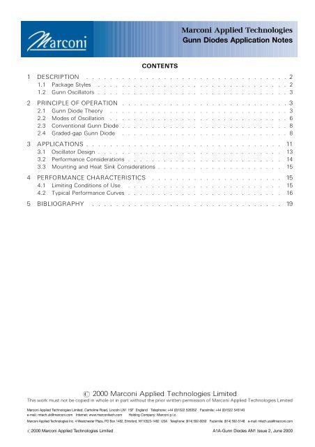
CONTENTS<br />
1 DESCRIPTION . . . . . . . . . . . . . . . . . . . . . . . . . . . . . . . . . . 2<br />
1.1 Package Styles . . . . . . . . . . . . . . . . . . . . . . . . . . . . . . . . 2<br />
1.2 <strong>Gunn</strong> Oscillators . . . . . . . . . . . . . . . . . . . . . . . . . . . . . . . . 3<br />
2 PRINCIPLE OF OPERATION . . . . . . . . . . . . . . . . . . . . . . . . . . . . 3<br />
2.1 <strong>Gunn</strong> Diode Theory . . . . . . . . . . . . . . . . . . . . . . . . . . . . . . 3<br />
2.2 Modes of Oscillation . . . . . . . . . . . . . . . . . . . . . . . . . . . . . . 6<br />
2.3 Conventional <strong>Gunn</strong> Diode . . . . . . . . . . . . . . . . . . . . . . . . . . . . 8<br />
2.4 Graded-gap <strong>Gunn</strong> Diode . . . . . . . . . . . . . . . . . . . . . . . . . . . . 8<br />
3 APPLICATIONS . . . . . . . . . . . . . . . . . . . . . . . . . . . . . . . . . 11<br />
3.1 Oscillator Design . . . . . . . . . . . . . . . . . . . . . . . . . . . . . . . 13<br />
3.2 Performance Considerations . . . . . . . . . . . . . . . . . . . . . . . . . . 14<br />
3.3 Mounting and Heat Sink Considerations . . . . . . . . . . . . . . . . . . . . . 15<br />
4 PERFORMANCE CHARACTERISTICS . . . . . . . . . . . . . . . . . . . . . . 15<br />
4.1 Limiting Conditions of Use . . . . . . . . . . . . . . . . . . . . . . . . . . 15<br />
4.2 Typical Performance Curves . . . . . . . . . . . . . . . . . . . . . . . . . . 16<br />
5 BIBLIOGRAPHY . . . . . . . . . . . . . . . . . . . . . . . . . . . . . . . . 19<br />
# 2000 <strong>Marconi</strong> <strong>Applied</strong> <strong>Technologies</strong> Limited<br />
This work must not be copied in whole or in part without the prior written permission of <strong>Marconi</strong> <strong>Applied</strong> <strong>Technologies</strong> Limited<br />
<strong>Marconi</strong> <strong>Applied</strong> <strong>Technologies</strong> Limited, Carholme Road, Lincoln LN1 1SF England Telephone: +44 (0)1522 526352 Facsimile: +44 (0)1522 545140<br />
e-mail: mtech.uk@marconi.com Internet: www.marconitech.com Holding Company: <strong>Marconi</strong> p.l.c.<br />
<strong>Marconi</strong> <strong>Applied</strong> <strong>Technologies</strong> Inc. 4 Westchester Plaza, PO Box 1482, Elmsford, NY10523-1482 USA Telephone: (914) 592-6050 Facsimile: (914) 592-5148 e-mail: mtech.usa@marconi.com<br />
#2000 <strong>Marconi</strong> <strong>Applied</strong> <strong>Technologies</strong> Limited A1A-<strong>Gunn</strong> <strong>Diodes</strong> AN1 Issue 2, June 2000
"<br />
1 DESCRIPTION<br />
The <strong>Gunn</strong> diode is the best known and most readily available<br />
device in the family of transferred electron devices (TED). They<br />
are employed as DC to microwave converters using the<br />
negative resistance characteristics of bulk Gallium Arsenide<br />
(GaAs) and only require a standard, low impedance, constant<br />
voltage power supply, thereby eliminating complex circuitry.<br />
The DC1200 series of GaAs <strong>Gunn</strong> diodes is designed for<br />
operation at fixed frequency (determined by the oscillator<br />
cavity) within a specified band under CW or pulsed conditions.<br />
Both conventional and hot electron injected (graded-gap) <strong>Gunn</strong><br />
diode designs are available (see Section 2). All devices feature<br />
low FM and AM noise characteristics and their wideband<br />
negative resistance enables them to be used in voltage<br />
controlled and mechanically tuned oscillators. The hot electron<br />
injected <strong>Gunn</strong> diodes offer the additional advantages of:<br />
* higher fundamental frequency operation,<br />
* increased efficiency,<br />
* improved temperature stability,<br />
* improved turn-on characteristic and<br />
* reduced FM sideband noise.<br />
Devices are available in either polarity, but are generally<br />
supplied as negative heat sink.<br />
1.1 Package Styles<br />
Several standard package styles are offered covering the<br />
frequency range 4 to 110 GHz and designed to suit different<br />
applications (see Fig. 1.1). Custom packaging requirements will<br />
also be considered upon request.<br />
The following package limitations need to be taken into<br />
consideration:<br />
Thermal Resistance<br />
The lowest thermal resistance is offered by the screw-based<br />
packages (outlines 40, 86 and 106). For high volume, lower<br />
power applications where oscillator assembly time is more<br />
important, non-threaded packages such as outline 00 will be<br />
preferred (refer to Mounting and Heat Sink Considerations -<br />
Section 3.3).<br />
Frequency Range<br />
The equivalent circuit diagram of a packaged <strong>Gunn</strong> diode is<br />
shown in Fig. 1.2. The magnitude of the parasitic impedances<br />
attributed to the package element reduces with the package<br />
size (004864106). Consequently, the larger, more robust<br />
package styles are normally specified for operation at lower<br />
frequencies and the smaller, low parasitic impedance packages<br />
are recommended for the higher frequency applications.<br />
Magnetically Tuned Circuits<br />
For applications involving magnetically (YIG) tuned oscillators,<br />
<strong>Gunn</strong> diodes can be supplied in Kovar-free packages.<br />
00<br />
"<br />
5.3/5.9<br />
"<br />
"<br />
11.52/1.63<br />
"<br />
"<br />
11.98/2.08<br />
"<br />
1.52/1.63 1.70/1.85 1.52/1.63 13.00/3.15<br />
"<br />
"<br />
"<br />
"<br />
"<br />
"<br />
"<br />
40<br />
"<br />
"<br />
0.75/0.85<br />
3-48 UNC 2A THREAD<br />
0.22/0.28<br />
"<br />
"<br />
"<br />
0.53/0.63<br />
"<br />
12.05/2.15<br />
12.95/3.00<br />
"<br />
"<br />
"<br />
"<br />
"<br />
12.45/2.55<br />
5.28 MAX<br />
"<br />
"<br />
"<br />
Fig. 1.1 Standard <strong>Gunn</strong> Diode Package Outlines (continued on page 3)<br />
<strong>Gunn</strong> <strong>Diodes</strong> AN1, page 2<br />
#2000 <strong>Marconi</strong> <strong>Applied</strong> <strong>Technologies</strong>
86<br />
"<br />
4.0/4.5<br />
"<br />
0.63/0.78<br />
"<br />
"<br />
0.46/0.56<br />
"<br />
"<br />
"<br />
"<br />
11.22/1.32<br />
"<br />
12.49/2.59<br />
"<br />
"<br />
3-48 UNC 2A THREAD<br />
106<br />
"<br />
3.5/3.7<br />
"<br />
"<br />
"<br />
0.47/0.57<br />
"<br />
12.89/3.00<br />
"<br />
"<br />
10.72/0.90<br />
"<br />
"<br />
3-48 UNC 2A THREAD<br />
"<br />
"<br />
0.31/0.47<br />
1.2 <strong>Gunn</strong> Oscillators<br />
<strong>Marconi</strong> <strong>Applied</strong> <strong>Technologies</strong> designs and manufactures a<br />
range of oscillator products using <strong>Marconi</strong> <strong>Gunn</strong> diodes.<br />
Standard products include a range of fixed frequency and<br />
mechanically or electronically tuned oscillators. Enquiries are<br />
welcomed for oscillator products that are not in the standard<br />
range.<br />
7504<br />
R S L P<br />
C P<br />
2 PRINCIPLE OF OPERATION<br />
2.1 <strong>Gunn</strong> Diode Theory<br />
In order to understand the nature of the transferred electron<br />
effect exhibited by <strong>Gunn</strong> diodes, it is necessary to consider the<br />
electron drift velocity versus electric field (or current versus<br />
voltage) relationship for GaAs (see Fig. 2.1).<br />
Below the threshold field, E th , of approximately 0.32 V/mm, the<br />
device acts as a passive resistance. However, above E th the<br />
electron velocity (current) decreases as the field (voltage)<br />
increases producing a region of negative differential mobility,<br />
NDM (resistance, NDR). This is the essential feature that leads<br />
to current instabilities and <strong>Gunn</strong> oscillations in an active device<br />
and is due to the special conductance band structure of direct<br />
band gap semiconductors such as Gallium Arsenide (see Fig.<br />
2.2).<br />
7R G<br />
C G<br />
"<br />
7486<br />
"<br />
DIODE ELEMENT<br />
PACKAGE ELEMENT<br />
C P = PACKAGE CAPACITANCE<br />
L P = BOND LEAD INDUCTANCE<br />
R S = SERIES RESISTANCE<br />
7R G = GUNN DIODE RESISTANCE<br />
C G = GUNN DIODE CAPACITANCE<br />
"<br />
DRIFT VELOCTY v (CURRENT)<br />
E th<br />
0.32V/mm<br />
ELECTRIC FIELD E (VOLTAGE)<br />
E H<br />
"<br />
Fig. 1.2<br />
Simple Equivalent Circuit for a Packaged <strong>Gunn</strong><br />
Diode<br />
Fig. 2.1 The Electric Field Dependent Average Drift<br />
Velocity for N-type GaAs<br />
#2000 <strong>Marconi</strong> <strong>Applied</strong> <strong>Technologies</strong> <strong>Gunn</strong> <strong>Diodes</strong> AN1, page 3
4<br />
7487<br />
T = 300K<br />
3<br />
CONDUCTION BAND<br />
SATELLITE X<br />
VALLEY<br />
2<br />
SATELLITE L<br />
VALLEY<br />
"<br />
"<br />
"<br />
DE = 0.31 eV<br />
"<br />
"<br />
"<br />
1<br />
LOWER G<br />
VALLEY<br />
E g = 1.42 eV<br />
0<br />
"<br />
VALENCE BAND<br />
71<br />
ENERGY (eV)<br />
72<br />
L [111] G " [100]<br />
"<br />
X<br />
Fig. 2.2<br />
The Band Structure of GaAs at 300 K<br />
The energy-momentum relationship contains two conduction<br />
band energy levels, G and L (also known as valleys) with the<br />
following properties:<br />
* In the lower G valley, electrons exhibit a small effective<br />
mass and very high mobility, m 1 .<br />
* In the satellite L valley, electrons exhibit a large effective<br />
mass and very low mobility, m 2 .<br />
* The two valleys are separated by a small energy gap, DE,<br />
of approximately 0.31 eV.<br />
In equilibrium at room temperature most electrons reside near<br />
the bottom of the lower G valley. Because of their high mobility<br />
(* 8000 cm 2 V -1 s -1 ), they can readily be accelerated in a strong<br />
electric field to energies in the order of the G-L intervalley<br />
separation, DE. Electrons are then able to scatter into the<br />
satellite L valley, resulting in a decrease in the average electron<br />
mobility, m, as given below:<br />
m =(n 1 .m 1 +n 2 .m 2 )/(n 1 +n 2 )<br />
where n 1 = electron density in G valley<br />
n 2 = electron density in L valley<br />
Above the high field, E H , most electrons reside in the L valley<br />
and the device behaves as a passive resistance (of greater<br />
magnitude) once again.<br />
In a practical <strong>Gunn</strong> diode, electrons are accelerated from the<br />
cathode by the prevailing electric field. When they have<br />
acquired sufficient energy, they begin to scatter into the low<br />
mobility satellite valley and slow down. This charge fluctuation<br />
<strong>Gunn</strong> <strong>Diodes</strong> AN1, page 4<br />
#2000 <strong>Marconi</strong> <strong>Applied</strong> <strong>Technologies</strong>
esults in a localised increase in the electric field and a<br />
corresponding decrease (to below the threshold value)<br />
elsewhere within the sample. Electrons ahead of the region still<br />
exhibit high mobility and move away from the charge<br />
fluctuation causing a depletion of carriers. Electrons behind<br />
the charge fluctuation, are also moving faster and accumulate<br />
behind the depleted region causing a dipole (or high field)<br />
domain (see Fig. 2.3), which grows in amplitude.<br />
A fall in current is associated with the domain growth due to its<br />
reduced mobility. The domain propagates through the sample<br />
at a constant velocity (*1 x 10 7 cm.s 71 for GaAs) until it<br />
reaches the anode where it collapses. As the domain collapses,<br />
the electric field outside the domain rises and the current in the<br />
external circuit increases until the threshold field is reached<br />
again and a new domain is formed.<br />
For a given doping density there will be a minimum device<br />
length that will support a domain due to the finite time required<br />
for domain growth. If this time is longer than that required for<br />
the domain to traverse the sample, then domain formation will<br />
not occur. Similarly, if the doping density is too high, then the<br />
current (and hence the temperature) in the semiconductor<br />
becomes too great and the life expectancy of the device is<br />
reduced. In practice, the product of doping density, n, and<br />
device length, l, is maintained between the following limits:<br />
1x10 12 cm 72 4 n.l 4 2x10 12 cm 72<br />
SPACE CHARGE<br />
"<br />
7488 ACCUMULATION LAYER<br />
"<br />
DEPLETION LAYER<br />
"<br />
0<br />
CATHODE<br />
"<br />
DISTANCE<br />
ANODE<br />
ELECTRIC FIELD<br />
"<br />
E th<br />
E H<br />
E L<br />
ANODE<br />
0<br />
CATHODE<br />
DISTANCE<br />
"<br />
Fig. 2.3<br />
The Band Structure of GaAs at 300 K<br />
#2000 <strong>Marconi</strong> <strong>Applied</strong> <strong>Technologies</strong> <strong>Gunn</strong> <strong>Diodes</strong> AN1, page 5
2.2 Modes of Oscillation<br />
2.2.1 Transit Time Mode<br />
This is the basic diode oscillation mode and is independent of<br />
the external circuit. Current peaks are obtained when a domain<br />
is quenched at the anode, after which another is nucleated near<br />
the cathode. The frequency is determined by the domain transit<br />
time, T t :<br />
T t = l/v D<br />
where l = length of device<br />
v D = domain velocity (* 1x10 7 cm.s -1 )<br />
so frequency, f t :<br />
f t = 1/T t =v D /l<br />
This mode of operation was first reported by (and is named<br />
after) J. B. <strong>Gunn</strong> in 1963. Its main characteristics are (see Fig.<br />
2.4):<br />
* The total electric field across the device at any time is<br />
above the threshold value.<br />
* The current waveform consists of narrow spikes, indicating<br />
a high harmonic content and low efficiency at fundamental<br />
frequency.<br />
* The RF field across the device is small, indicating low<br />
impedance.<br />
* The transit time frequency is a strong function of operating<br />
voltage and temperature.<br />
Therefore the transit time mode has poor stability and<br />
efficiency.<br />
7489<br />
I<br />
"<br />
I p<br />
E 0<br />
T t<br />
t<br />
I v<br />
"<br />
"<br />
"<br />
E th<br />
"<br />
E<br />
t<br />
"<br />
Fig. 2.4<br />
Current and Field Waveforms for Transit Time Mode<br />
<strong>Gunn</strong> <strong>Diodes</strong> AN1, page 6<br />
#2000 <strong>Marconi</strong> <strong>Applied</strong> <strong>Technologies</strong>
2.2.2 Delayed Domain Mode<br />
Fig. 2.5 shows the basic voltage and current waveforms for this<br />
mode of operation. Unlike the transit time mode, the total<br />
electric field across the device drops below the threshold value,<br />
E th , during part of the RF cycle, such that nucleation of a new<br />
domain is delayed.<br />
As soon as the field rises above E th , a domain nucleates at the<br />
cathode and travels across the device. As the field swings<br />
below E th , the domain arrives at the anode and decays its<br />
charge. A new domain cannot form at the cathode until the<br />
field rises above E th again. This delay time between extinction<br />
and creation of domains modifies the operating frequency, f d ,<br />
to:<br />
f d = 1/(T t +T d )<br />
where T t = transit time<br />
T d = delay time<br />
The transit time is a fixed quantity for a given device, but the<br />
delay time is a function of the RF voltage, which is determined<br />
by an external circuit. It follows that the operating frequency is<br />
always below the transit time frequency.<br />
The important characteristics of this mode of operation are:<br />
* The total electric field across the device is below the<br />
threshold field, E th , over a part of the RF cycle.<br />
* The current waveform consists of broad spikes, indicating<br />
a low harmonic content and higher efficiency at<br />
fundamental frequency.<br />
* The RF field across the device is large, indicating high<br />
impedance.<br />
* The operating frequency is determined mainly by the<br />
resonant frequency of the external circuit and can be made<br />
very stable. A device can also be used over a much<br />
broader bandwidth below the transit time frequency.<br />
This mode of operation is therefore most commonly used in the<br />
majority of commercial applications.<br />
7490<br />
I<br />
"<br />
I p<br />
I v<br />
t<br />
E 0<br />
"<br />
T d T t<br />
" "<br />
"<br />
E th<br />
"<br />
E<br />
t<br />
"<br />
Fig. 2.5<br />
Current and Field Waveforms for Delayed Domain Mode<br />
#2000 <strong>Marconi</strong> <strong>Applied</strong> <strong>Technologies</strong> <strong>Gunn</strong> <strong>Diodes</strong> AN1, page 7
2.3 Conventional <strong>Gunn</strong> Diode<br />
A conventional <strong>Gunn</strong> diode generally consists of three layers; a<br />
relatively low doped transit region sandwiched between two<br />
highly doped contact regions, forming an n + -n- + structure<br />
(see Fig. 2.6). The device is defined basically by five<br />
parameters:<br />
n The doping concentration in the transit region of the<br />
Gallium Arsenide.<br />
l The thickness of the transit region.<br />
R 0 The low field resistance of the diode measured close to<br />
the origin.<br />
I th Threshold current. This is the maximum current through<br />
the device and can exceed the operating current by as<br />
much as 50%.<br />
NB. The power supply must be capable of passing<br />
through this point.<br />
V th Threshold voltage. The voltage at the current<br />
maximum.<br />
The ratio 7R G /R 0 is an important circuit design parameter. V th<br />
and I th are independent of the external circuit and may be<br />
measured with the diode in any good heat sink. Because V th is<br />
measured on the flat part of the curve, the measuring technique<br />
must be carefully specified to avoid error.<br />
7491<br />
I<br />
I th<br />
"<br />
R 0<br />
The frequency of the <strong>Gunn</strong> diode is determined primarily by the<br />
transit region length, l. However, a portion of this region is used<br />
to accelerate the electrons from the cathode until they have<br />
sufficient energy to enter the low mobility state and does not<br />
support domain formation. This ‘dead zone’ may be as much as<br />
0.25 mm in a transit region length of 1.5 mm (for a millimetric<br />
diode) and, because it acts as a parasitic resistance, results in<br />
reduced efficiency. For conventional <strong>Gunn</strong> diodes there is a<br />
rapid fall-off in power at frequencies above 60 GHz, where the<br />
less efficient second harmonic component of the power has to<br />
be utilised.<br />
The starting voltage must be well below the required operating<br />
voltage (typically V op = 3 x V th ), particularly when low<br />
temperature operation is required, as the starting voltage rises<br />
with falling temperature. This can be controlled to some extent<br />
by the correct choice of n and l, but severely restricts the use of<br />
conventional <strong>Gunn</strong> diodes at temperatures below about 725 8C.<br />
The turn-on voltage, V on (the voltage above threshold at which<br />
coherent RF power is obtained), increases to the point where it<br />
equals the peak power voltage V pk (see Fig. 2.7a). This forces<br />
the diode to be operated at a higher voltage with corresponding<br />
loss in power, reduced efficiency, poor FM sideband noise and<br />
the increased possibility of device failure.<br />
2.4 Graded-gap <strong>Gunn</strong> Diode<br />
The limitations of the conventional <strong>Gunn</strong> diode (described<br />
earlier) can be overcome by injecting high energy, ‘hot<br />
electrons’, into the transit region. The concept is to introduce<br />
electrons into a region so that the temperature, which describes<br />
their energy distribution, is much greater than that of the<br />
semiconductor lattice. In the graded-gap <strong>Gunn</strong> diode, electrons<br />
are injected into the transit region with an energy equal to that<br />
of the G-L intervalley separation so that stable domains will<br />
form very near to the cathode and move across the transit<br />
region as soon as the field is high enough to sustain<br />
accumulation and propagation. The dead zone is effectively<br />
eliminated and the transit length is fixed and independent of<br />
bias. Therefore, coherent power can be generated over a wide<br />
range of operating voltages (see Fig. 2.7b).<br />
V th<br />
"<br />
V<br />
7492<br />
n ++ n ++<br />
DOPING DENSITY<br />
"<br />
"<br />
l<br />
"<br />
n<br />
OHMIC<br />
CONTACT<br />
TRANSIT REGION<br />
SUBSTRATE<br />
OHMIC<br />
CONTACT<br />
Fig. 2.6<br />
Structural Schematic and Current-Voltage Relationship for a Conventional <strong>Gunn</strong> Diode<br />
<strong>Gunn</strong> <strong>Diodes</strong> AN1, page 8<br />
#2000 <strong>Marconi</strong> <strong>Applied</strong> <strong>Technologies</strong>
V on V pk<br />
7493<br />
POWER (mW)<br />
50<br />
"<br />
"<br />
25<br />
0<br />
0<br />
a)<br />
1 2 3 4 5 6<br />
VOLTAGE (V)<br />
V pk<br />
50<br />
"<br />
POWER (mW)<br />
25<br />
V on<br />
"<br />
0<br />
0<br />
b)<br />
1 2 3 4 5 6<br />
VOLTAGE (V)<br />
Fig. 2.7<br />
Typical Turn-on Characteristic of: a) Conventional <strong>Gunn</strong> Diode and b) Graded-gap <strong>Gunn</strong> Diode<br />
There are a variety of possible structures which can be used for<br />
hot electron injection. To produce microwave power with as<br />
little bias dependence as possible, the optimum injector shape<br />
has a slowly increasing potential with an abrupt drop back to<br />
the transit region value. This is best realised with a graded-gap<br />
injector (see Fig. 2.8). Simulations have shown that a thin n +<br />
layer between the injector and the transit region is critical for<br />
controlling the electric field, while retaining the hot electron<br />
properties. Fig. 2.8b shows the n + spike depleted giving an<br />
injection energy of DE.<br />
An additional benefit from using a graded-gap <strong>Gunn</strong> diode is<br />
the much improved temperature stability. This is due to the<br />
electron temperature being set by the injection energy, typically<br />
equivalent to 2000 K. Changes in the substrate temperature in<br />
the 130 8C range usually required for military specifications, etc,<br />
are relatively small in comparison.<br />
The structural schematic and current-voltage relationship for a<br />
graded-gap <strong>Gunn</strong> diode are shown in Fig. 2.9. Under forward<br />
bias, the peak current is much less defined due to the action of<br />
the cathode injector (i.e. significant numbers of electrons<br />
already reside in the upper valley when entering the transit<br />
region) and the gradient of the curve beyond threshold is<br />
shallower.<br />
#2000 <strong>Marconi</strong> <strong>Applied</strong> <strong>Technologies</strong> <strong>Gunn</strong> <strong>Diodes</strong> AN1, page 9
7494<br />
n + SPIKE<br />
BIAS = 0<br />
"<br />
CONTACT INJECTOR TRANSIT REGION CONTACT<br />
"<br />
"<br />
"<br />
"<br />
"<br />
"<br />
a)<br />
e 7<br />
"<br />
"<br />
GRADED<br />
GAP<br />
"<br />
*DE<br />
BIAS = V<br />
V<br />
"<br />
"<br />
n + n + n 7<br />
n +<br />
b)<br />
Fig. 2.8 A Schematic Diagram of a Hot Electron Injector <strong>Gunn</strong> Diode under a) Zero Bias, and b) Forward Bias V.<br />
7495<br />
REVERSE<br />
1<br />
FORWARD<br />
CURRENT (A)<br />
0<br />
0<br />
1 2 3 4<br />
BIAS (V)<br />
7496<br />
n ++ n + n ++<br />
DOPING DENSITY<br />
"<br />
"<br />
l<br />
"<br />
n<br />
OHMIC<br />
CONTACT<br />
GRADED<br />
AlGaAs<br />
TRANSIT REGION<br />
SUBSTRATE<br />
OHMIC<br />
CONTACT<br />
Fig. 2.9<br />
Structural Schematic and Current-Voltage Relationship for a Graded-gap <strong>Gunn</strong> Diode<br />
<strong>Gunn</strong> <strong>Diodes</strong> AN1, page 10<br />
#2000 <strong>Marconi</strong> <strong>Applied</strong> <strong>Technologies</strong>
Graded-gap <strong>Gunn</strong> diodes have demonstrated room temperature<br />
performance of up to 80 mW and 2.4% efficiency at 90 GHz;<br />
the best results achieved for mm-wave GaAs devices at this<br />
frequency. 50 - 60 mW at 94 GHz, with efficiencies of 1.6%, is<br />
reproducibly achieved (see Table 2.1). FM sideband noise is<br />
better than 780 dBc/Hz, 100 kHz from carrier, equal to that<br />
obtained from the best conventional devices. Significantly<br />
these devices exhibit a turn-on voltage very close to threshold<br />
(see Figure 2.7b), which allows coherent oscillations around<br />
peak power over the full military specification temperature<br />
range. Further evidence of the improved temperature stability<br />
can be seen from the power, frequency and peak power<br />
variations across this temperature range, generally a factor of<br />
two or more below that exhibited by devices without hot<br />
electron injection. This is an added bonus for VCO designers<br />
who can then utilise a larger bandwidth, because there is no<br />
longer need to compensate for frequency drift with<br />
temperature.<br />
Freq<br />
(GHz)<br />
Temp<br />
(8C)<br />
V on<br />
(V)<br />
V op<br />
(V)<br />
I op<br />
(mA)<br />
Power<br />
(mW)<br />
Eff<br />
(%)<br />
Noise *<br />
(dBc/Hz)<br />
90 740 3.9 4.9 680 58 1.75<br />
90 +25 3.2 4.7 660 50 1.6 786<br />
90 +80 3.1 4.8 640 42 1.4<br />
3 APPLICATIONS<br />
<strong>Gunn</strong> diodes are reliable, relatively easy to install and the lower<br />
output power levels fall well below the safety exposure limits.<br />
They are ideally suited for use in low noise sources such as local<br />
oscillators, locking oscillators, low and medium power<br />
transmitter applications and motion detection systems. Higher<br />
power varieties can be used in phase-locked oscillators or as<br />
reflection amplifiers in point-to-point communication links and<br />
telemetry systems.<br />
Microwave sources have the advantages over ultrasonic<br />
detectors of size and beamwidth, and over optical systems of<br />
working in dusty and adverse environments. The low voltage<br />
requirements of <strong>Gunn</strong> oscillators mean that battery or regulated<br />
mains supplies may be used, (battery drain can be reduced by<br />
using low current devices or by operation in a pulsed mode).<br />
However, microwaves are reflected from metal surfaces and<br />
partially reflected from many others e.g. brick, Tarmac and<br />
concrete, and they are attenuated by oxygen, water or water<br />
vapour. Figure 3.1 shows attenuation effects in the frequency<br />
range of interest.<br />
94 +25 3.0 4.5 600 60 2.0 788<br />
60 +25 3.0 4.5 600 120 5.0 790<br />
35 +25 3.0 4.5 1300 350 5.5 795<br />
* 100kHz offset frequency<br />
Table 2.1 Typical Performance of Graded-gap GaAs <strong>Gunn</strong><br />
<strong>Diodes</strong><br />
FREQUENCY (GHz)<br />
10 15<br />
30<br />
60 70 95 100 150 220 300<br />
100<br />
183 GHz<br />
60 GHz<br />
7497<br />
ATTENUATION (dB/km)<br />
10<br />
1.0<br />
0.1<br />
SEA LEVEL<br />
"<br />
22 GHz<br />
"<br />
"<br />
0 2<br />
118 GHz<br />
0 2<br />
"<br />
H 2 0<br />
0.01<br />
0.001<br />
"<br />
"<br />
H 2 0<br />
4km<br />
ITU REGION 2 RADIOLOCATION BANDS<br />
"<br />
"<br />
IEEE RADAR LETTERBANDS<br />
X Ku K Ka mm<br />
30 20<br />
10<br />
5<br />
3<br />
2 1<br />
WAVELENGTH (mm)<br />
Fig. 3.1<br />
Atmospheric attenuation at millimetre wavelengths with IEEE radar letterbands and ITU radiolocation bands for<br />
region 2 (after Altshuler et al)<br />
#2000 <strong>Marconi</strong> <strong>Applied</strong> <strong>Technologies</strong> <strong>Gunn</strong> <strong>Diodes</strong> AN1, page 11
The range of application of <strong>Gunn</strong> sensors for industrial and<br />
commercial use is extensive and the following is only a brief list:<br />
Collision avoidance radar<br />
Vehicle ABS<br />
Traffic analyser sensors<br />
‘Blind spot’ car radar<br />
Pedestrian safety systems<br />
Elapsed distance meters<br />
Automatic identification<br />
Presence/absence indicators<br />
Movement sensors<br />
Distance measurements<br />
Slow-speed sensors<br />
Level sensors<br />
Traffic signal actuators<br />
Proximity movement detectors<br />
Door opening sensors<br />
Barrier operation<br />
Process control devices (object counting)<br />
Intruder/burglar alarms<br />
Perimeter protection<br />
Train derailment sensors<br />
Contactless vibration transducers<br />
Rotational speed tachometers<br />
Linear distance indicators<br />
Moisture content measurement<br />
Table 3.1 indicates the most commonly used <strong>Gunn</strong> diode types<br />
by application.<br />
APPLICATION<br />
Local Oscillators:<br />
Radar<br />
Fast tunable ECM<br />
Diode noise measurement<br />
Telecommunications:<br />
Transmitters<br />
Low noise oscillators<br />
Point-to-point links<br />
Control devices:<br />
Railway crossings<br />
Traffic control<br />
Vehicle ABS<br />
Door openers<br />
Motion detectors:<br />
Speed control<br />
Radar detectors<br />
Intruder alarms<br />
Shoreline navigation<br />
Low Power<br />
Fixed Frequency CW Broadband CW Pulsed<br />
High Power<br />
Low Frequency High Frequency<br />
*<br />
*<br />
*<br />
*<br />
*<br />
*<br />
*<br />
*<br />
* *<br />
*<br />
*<br />
*<br />
*<br />
Transmitters:<br />
Radar transponders<br />
Missile beacons<br />
Radio link exciters *<br />
Injection locked amplifiers *<br />
Paramp pump sources *<br />
Instrumentation *<br />
*<br />
*<br />
*<br />
*<br />
Table 3.1<br />
<strong>Gunn</strong> Diode Selection Chart<br />
<strong>Gunn</strong> <strong>Diodes</strong> AN1, page 12<br />
#2000 <strong>Marconi</strong> <strong>Applied</strong> <strong>Technologies</strong>
7498<br />
"<br />
RF<br />
DIODE<br />
"<br />
RF<br />
IRIS<br />
DIODE<br />
"<br />
*lg/2<br />
"<br />
"<br />
*lg/2<br />
"<br />
Fig. 3.2<br />
Basic Microwave Cavity Design<br />
3.1 Oscillator Design<br />
The natural frequency of oscillation of the <strong>Gunn</strong> diode can be<br />
altered to some extent by the external circuit. The formation or<br />
premature collapse of a domain within a cycle can be<br />
controlled, and hence the power, frequency and efficiency<br />
adjusted. Control of the frequency by external means rather<br />
than by device parameters only is essential for a stable<br />
oscillator. The external cavity used to resonate the device<br />
negative impedance can be coaxial, waveguide, microstrip, YIG<br />
crystal, etc, depending on the required application.<br />
Generally, coaxial and microstrip circuits offer low Q values<br />
with poor noise and stability performance, resulting in the<br />
frequency of oscillation changing with load and environmental<br />
variations. YIG crystal tuned circuits are usually too expensive<br />
for commercial and industrial applications and therefore the<br />
most common cavity is waveguide. Usually the <strong>Gunn</strong> diode is<br />
mounted on a post structure between the waveguide walls,<br />
either lg/2 from an iris or lg/2 from a short circuit (see Fig.<br />
3.2). Some alteration is necessary to set the exact frequency to<br />
allow for diode and package parasitics and manufacturing<br />
tolerances. Tuning screws of either metal or dielectric are used<br />
to modify the cavity resonant frequency. Power output<br />
variations are achieved by adjusting the coupling between<br />
diode and load using variations in post size or tuning screws.<br />
A more detailed schematic of a packaged <strong>Gunn</strong> diode mounted<br />
in a radial disc, microwave cavity and its equivalent circuit<br />
diagram are given in Figs. 3.3 and 3.4.<br />
BACKSHORT<br />
GUNN DIODE<br />
"<br />
7499<br />
"<br />
v<br />
"<br />
"<br />
"<br />
BIAS CHOKE<br />
FILTER<br />
WAVEGUIDE<br />
RADIAL DISC<br />
Fig. 3.3 The Packaged <strong>Gunn</strong> Diode Mounted in a<br />
Microwave Cavity (approximately half scale).<br />
7500<br />
BIAS<br />
CHOKE<br />
FILTER<br />
WAVEGUIDE<br />
BACKSHORT<br />
L P<br />
DISC<br />
LOAD<br />
-R G<br />
L B<br />
C P<br />
C D<br />
C S<br />
Fig. 3.4<br />
An Equivalent Circuit Diagram for the <strong>Gunn</strong> Diode, Package, Disc and Cavity<br />
#2000 <strong>Marconi</strong> <strong>Applied</strong> <strong>Technologies</strong> <strong>Gunn</strong> <strong>Diodes</strong> AN1, page 13
Most simple <strong>Gunn</strong> oscillators are designed empirically using a<br />
few ground rules and a lot of experience. The designs have to<br />
tolerate batch to batch variations in diode parameters and have<br />
the required stability. They must not present the diode with an<br />
RF impedance such that the device takes DC power but<br />
produces no RF output, thus leading to a possible turn-on or<br />
switch-on failure.<br />
A recommended <strong>Gunn</strong> diode driver circuit is shown in Fig. 3.5<br />
V S<br />
Fig. 3.5<br />
R<br />
I R<br />
I B<br />
I Z<br />
"<br />
"<br />
"<br />
"<br />
7501<br />
I R =I B +I Z<br />
I B =I sat /h fe<br />
R=(V S 7V Z1 )/I R<br />
V Z1 =V G0 + 0.7 V<br />
C 1 = 0.1 mF<br />
G 1 = <strong>Gunn</strong> diode<br />
Z 1 ,Z 2 = Zener diode<br />
V Z2 =V G max<br />
V Z1 VZ2 V G0<br />
Z 1 Z 2 C 1<br />
G 1<br />
A Recommended <strong>Gunn</strong> Diode Drive Circuit<br />
3.2 Performance Considerations<br />
3.2.1 Matching<br />
The <strong>Gunn</strong> diode is a current generator and needs matching into<br />
the circuit for optimum output power, noise, smooth tuning<br />
and power-temperature variation. Small differences may exist<br />
even between cavities which are nominally identical. Testing in<br />
the customer’s own cavity design is always the preferred<br />
solution.<br />
The impedance matching problem becomes increasingly critical<br />
as the cavity Q goes up. The impedance of the diode is<br />
determined to the first order by the thickness, doping and<br />
operating voltage. However, second order trimming can be<br />
obtained by varying the voltage to alter the domain width, and<br />
therefore the domain capacitance, by field control. The voltage<br />
at which maximum power is obtained is cavity dependent. If<br />
the diode is not well matched to the cavity, there may be a<br />
conflict between the voltage for correct match and the voltage<br />
at which the diode would want to operate in a low Q cavity.<br />
Trimming the diode parameters, therefore, becomes more<br />
critical as Q increases and the tolerances on device<br />
specifications become correspondingly tighter. It follows that it<br />
is more difficult to design a diode to work in a high Q cavity<br />
without having access to the cavity.<br />
3.2.2 Starting Voltage<br />
The conventional <strong>Gunn</strong> diode is a broadband negative<br />
resistance device and random noise is required to start it.<br />
Starting becomes more difficult at low temperature and in high<br />
Q cavities. High Q operation also means higher voltage<br />
operation for reliable starting. These limitations can be<br />
overcome (at higher frequencies) by the use of a graded-gap,<br />
current injected <strong>Gunn</strong> diode.<br />
3.2.3 Operating Current<br />
Increasing the operating current increases the output power.<br />
However, the maximum safe operating current for an<br />
encapsulated device is limited by the corresponding increase in<br />
the transit region temperature (9250 8C). This, in turn, is<br />
determined by the thermal resistance of the diode itself and by<br />
the effectiveness of the package heat sink (see Section 3.3).<br />
The lower limit of current is more difficult to define because the<br />
series resistance of the ohmic contact increases non-linearly as<br />
the diode area decreases.<br />
3.2.4 Output Power<br />
The output power is determined primarily by the diode area and<br />
the doping level. The highest power/efficiency is achieved<br />
using an integral heat sink (IHS) construction. This has the<br />
advantage of a thick, gold plated heat sink formed directly onto<br />
the epitaxial region and a minimal thickness of remaining<br />
substrate, thereby reducing the parasitic resistance. Further<br />
improvement in output power can be obtained at higher<br />
frequencies by the use of a graded-gap, current injected <strong>Gunn</strong><br />
diode.<br />
The upper limit on power handling is mainly determined by the<br />
dissipation of DC power through the package heat sink and the<br />
fact that the diode impedance becomes low and is difficult to<br />
match.<br />
3.2.5 FM Noise and dF/dT<br />
FM noise measurements are given as noise to carrier ratios (N/<br />
C) versus carrier offset modulation frequency, f m . The<br />
frequency deviation, Df, is calculated from:<br />
N/C = 20.log (Df.H2 /f m )<br />
where values of (N/C) are given in dBc/Hz.<br />
In the graded-gap <strong>Gunn</strong> diode, the variation in position at which<br />
domain formation occurs is much less than in a conventional<br />
device. Associated with this is a reduction in the variance of the<br />
first intervalley scattering effect for electrons entering the<br />
cathode region and hence a reduction in noise.<br />
The factors controlling FM noise and the<br />
frequency-temperature coefficient are complex and are<br />
resolved by work involving both the diode and oscillator<br />
design. The equivalent circuit of both the diode and the cavity<br />
form a total circuit concept and there is a trade-off between the<br />
parameters in each component. Oscillators and diodes need to<br />
be designed together to achieve given second order aspects of<br />
the specification.<br />
Second order effects such as noise, chirp, dF/dT, etc., bear no<br />
direct relationship to the primary characteristics of frequency<br />
and power. The secondary parameters can show wide variation<br />
between diodes, which in all other primary respects are<br />
identical.<br />
<strong>Gunn</strong> <strong>Diodes</strong> AN1, page 14<br />
#2000 <strong>Marconi</strong> <strong>Applied</strong> <strong>Technologies</strong>
3.2.6 Pulse <strong>Diodes</strong><br />
These diodes are even more cavity dependent than CW diodes.<br />
Whereas a conventional CW diode requires as low a series<br />
resistance as possible, this is not true in pulse diodes. The<br />
constant re-nucleation of domains at the start of each pulse<br />
requires closer control of the electric field at the cathode.<br />
Various methods of achieving this are available, including<br />
adding series resistance with a disc or by partially alloying the<br />
contacts to provide some non-ohmic behaviour. Alternatively, a<br />
graded-gap, current injected <strong>Gunn</strong> device may be used.<br />
Frequency change during the pulse (chirp) is also affected by<br />
these measures as is the dF/dT with which it correlates.<br />
Pulse diode noise is normally defined as the degradation in the<br />
Fourier sin(x)/x display of the RF power pulse from the ideal<br />
rectangular pulse values. The factors that control pulse noise<br />
and chirp are complex and the solution in any particular case is<br />
arrived at by modifications both to the diode processing and<br />
oscillator design.<br />
3.2.7 Special Operating Conditions<br />
In all cases where the optimum unique frequency and power<br />
design parameters have to be modified to achieve some special<br />
condition of low or high temperature operation, restricted<br />
voltage or current consumption, or broadband tuning, then<br />
some loss of optimum performance results. There is always a<br />
trade-off to be made to meet a special operating condition.<br />
3.2.8 Low Harmonic <strong>Diodes</strong><br />
<strong>Diodes</strong> can be designed to meet low harmonic generation limits<br />
(if required by local regulations) by modifying the material<br />
specification. The extent to which the harmonics can be<br />
reduced, however, is limited by the cavity design and depends<br />
on the measurement technique.<br />
3.2.9 Broadband Operation<br />
<strong>Diodes</strong> can be specially designed by modifying the material<br />
properties and controlling the encapsulation parasitics to give a<br />
broadband tuning performance in a carefully defined cavity.<br />
This is achieved at the expense of output power and efficiency.<br />
3.2.10 High Temperature Operation<br />
<strong>Marconi</strong> <strong>Applied</strong> <strong>Technologies</strong>’ standard range of <strong>Gunn</strong> diodes<br />
can be used up to heat sink temperatures of 85 8C. At higher<br />
temperatures it is necessary to reduce the transit region doping<br />
level in order to ensure long life. This means that for the same<br />
current flowing through the device a larger die is used and<br />
greater cooling is achieved by the increased area of contact<br />
with the heat sink and the larger surface area for radiation. This<br />
affects other properties of the diode and may require further<br />
modifications to be made to the specification.<br />
3.3 Mounting and Heat Sink Considerations<br />
The increase in temperature between the diode heat sink and<br />
the semiconductor transit region is defined by:<br />
DT =R y (P in 7P out )<br />
The thermal drop between the ambient and the diode heat sink<br />
must also be taken into account to avoid exceeding the<br />
maximum transit region temperature of *250 8C. The transit<br />
region temperature may be computed as follows:<br />
T tr =T amb + DT case + DT<br />
=T amb + DT case +R y (P in 7P out )<br />
where: T tr = transit region temperature (4250 8C).<br />
T amb = ambient temperature.<br />
DT case = temperature difference between the diode<br />
heat sink and ambient at the operating power.<br />
R y = diode thermal resistance.<br />
In well designed packages, the temperature difference, DT case ,<br />
is usually less than 30 8C for an input power of about 15 W.<br />
4 PERFORMANCE CHARACTERISTICS<br />
4.1 Limiting Conditions of Use<br />
Temperature:<br />
operating (for standard types) . . . . 740 to +85 8C<br />
storage . . . . . . . . . . . . 755 to +150 8C<br />
Operating voltage . . . . each type is individually rated.<br />
<strong>Application</strong> of a bias voltage in excess of this value may lead to<br />
degradation in performance.<br />
#2000 <strong>Marconi</strong> <strong>Applied</strong> <strong>Technologies</strong> <strong>Gunn</strong> <strong>Diodes</strong> AN1, page 15
4.2 Typical Performance Curves<br />
7502<br />
1.5<br />
1.5<br />
I TH<br />
0 1 2<br />
1.0<br />
1.0<br />
I TH<br />
CURRENT (A)<br />
0.5<br />
0<br />
Fig. 4.1<br />
0 1 V TH 2<br />
3 4 V op 5<br />
BIAS VOLTAGE<br />
a)<br />
CURRENT (A)<br />
0.5<br />
0<br />
BIAS VOLTAGE<br />
b)<br />
Typical DC Characteristic a) Standard <strong>Gunn</strong> Diode, b) Graded-gap <strong>Gunn</strong> Diode<br />
V TH 3 4 V op 5<br />
7503<br />
OUTPUT POWER PO (mW)<br />
300<br />
Df<br />
200<br />
300<br />
200<br />
100<br />
0<br />
7100<br />
7200<br />
7300<br />
100<br />
740 720 0 20 40 60 80<br />
CASE TEMPERATURE T (8C)<br />
P O<br />
FREQUENCY CHANGE Df (MHz)<br />
OUTPUT POWER PO (mW)<br />
a) b)<br />
110<br />
Df<br />
100<br />
P O<br />
280<br />
80<br />
0<br />
90<br />
7120<br />
740 720 0 20 40 60 80<br />
CASE TEMPERATURE T (8C)<br />
FREQUENCY CHANGE Df (MHz)<br />
30<br />
55<br />
40<br />
OUTPUT POWER PO (mW)<br />
20<br />
10<br />
0<br />
740<br />
720<br />
CASE TEMPERATURE T (8C)<br />
0<br />
P O<br />
20<br />
40<br />
Df<br />
60<br />
200<br />
100<br />
0<br />
7100<br />
80<br />
FREQUENCY CHANGE Df (MHz)<br />
OUTPUT POWER PO (mW)<br />
50<br />
Df<br />
45<br />
40<br />
35<br />
P O<br />
740 720 0 20 40 60 80<br />
CASE TEMPERATURE T (8C)<br />
0<br />
740<br />
780<br />
7120<br />
FREQUENCY CHANGE Df (MHz)<br />
c) d)<br />
Fig. 4.2<br />
Variation of Power and Frequency with Temperature for:<br />
a) DC1276H operating in the fundamental mode;<br />
b) DC1277G-T operating in the fundamental mode;<br />
c) DC1279D operating in the second harmonic mode;<br />
d) DC1279F-T operating in the second harmonic mode<br />
<strong>Gunn</strong> <strong>Diodes</strong> AN1, page 16<br />
#2000 <strong>Marconi</strong> <strong>Applied</strong> <strong>Technologies</strong>
1000<br />
100<br />
1000<br />
100<br />
P out<br />
P out<br />
Z eff<br />
P out<br />
Z eff<br />
100<br />
10<br />
100<br />
P out (1)<br />
10<br />
P out (2)<br />
Fig. 4.3<br />
POWER (mW)<br />
10<br />
Z EFFICIENCY<br />
1<br />
30 100<br />
FREQUENCY (GHz)<br />
Variation of power and frequency with temperature<br />
for DC1276 and DC1277 series.<br />
PERCENTAGE (%)<br />
Fig. 4.4<br />
POWER (mW)<br />
10<br />
Z EFFICIENCY (1)<br />
1<br />
30 100<br />
FREQUENCY (GHz)<br />
Z EFFICIENCY (2)<br />
Variation of power and efficiency for: 1) DC1278<br />
and DC1279 series; 2) DC1279F-T series<br />
PERCENTAGE (%)<br />
#2000 <strong>Marconi</strong> <strong>Applied</strong> <strong>Technologies</strong> <strong>Gunn</strong> <strong>Diodes</strong> AN1, page 17
+30<br />
+1<br />
CHANGE IN FREQUENCY (MHz)<br />
+20<br />
0<br />
POWER<br />
+10<br />
71<br />
0<br />
72<br />
710<br />
FREQUENCY<br />
73<br />
720<br />
8 9 10 11 12 74<br />
OPERATING VOLTAGE (V)<br />
CHANGE IN POWER (dB)<br />
Fig. 4.5<br />
Variation of output power and frequency with operating voltage<br />
15<br />
+3<br />
+2<br />
Fig. 4.6<br />
FREQUENCY (GHz)<br />
10<br />
5<br />
POWER<br />
VOLTAGE<br />
0<br />
73<br />
8 9 10 11 12<br />
OPERATING VOLTAGE (V)<br />
Effect of voltage tracking on the variation of output power with frequency on a wideband tunable waveguide<br />
oscillator.<br />
+1<br />
0<br />
71<br />
72<br />
CHANGE IN OUTPUT POWER (dB)<br />
I sat<br />
I op<br />
GUNN VOLTAGE<br />
CHANGE IN FREQUENCY (MHz)<br />
+10<br />
0<br />
710<br />
720<br />
Fig. 4.8<br />
730<br />
73<br />
720 710 0 +10 +20 +30 +40 +50 +60 +70<br />
TEMPERATURE (8C)<br />
FREQUENCY<br />
POWER<br />
+1<br />
Variation of frequency and power with temperature.<br />
0<br />
71<br />
72<br />
CHANGE IN POWER (dB)<br />
GUNN CURRENT<br />
V sat<br />
V op<br />
Fig. 4.7<br />
DC <strong>Gunn</strong> characteristics<br />
<strong>Gunn</strong> <strong>Diodes</strong> AN1, page 18<br />
#2000 <strong>Marconi</strong> <strong>Applied</strong> <strong>Technologies</strong>
5 BIBLIOGRAPHY<br />
Microwave Oscillation of Current in III-V Semiconductors.<br />
<strong>Gunn</strong> J.B.<br />
Solid State Commun., 1, 88 (1963).<br />
Theory of the <strong>Gunn</strong> Effect.<br />
Kroemer H.<br />
Proc. IEEE, 52, 1736 (1964).<br />
The <strong>Gunn</strong> Effect.<br />
Hobson G.S.<br />
Clarendon, Oxford, 1974.<br />
Theory of Stable Domain Propagation in the <strong>Gunn</strong> Effect.<br />
Butcher P.N.<br />
Phys. Lett., 19, 546 (1965).<br />
Transferred Electron Amplifiers and Oscillators for Microwave<br />
<strong>Application</strong>.<br />
Sterzer F.<br />
Proc. IEEE, 59, 1155 (1971).<br />
Hot Electron Microwave Generators.<br />
Carroll J.E.<br />
Arnold, 1970.<br />
Fundamental Mode graded-gap <strong>Gunn</strong> Diode Operation at 77<br />
and 84 GHz.<br />
Dale I., Stephens J.R.P., Bird J.<br />
Conf. Proc. Microwaves ‘94, .<br />
Advances in Hot Electron Injector <strong>Gunn</strong> diodes.<br />
Spooner H., Couch N.R.<br />
GEC J. of Res., 7, 34 (1989).<br />
Hot Electron Injection by Graded Al X Ga 1-X As.<br />
Long A.P., Beton P.H., Kelly M.J., Kerr T.M.<br />
Electronics Letters, 22, 130 (1986).<br />
Hot Electron Injection : Concept to Product.<br />
Couch N.R., Kelly M.J.<br />
Physics World, 2, 37 (1989).<br />
Whilst <strong>Marconi</strong> <strong>Applied</strong> <strong>Technologies</strong> has taken care to ensure the accuracy of the information contained herein it accepts no responsibility for the consequences of any<br />
use thereof and also reserves the right to change the specification of goods without notice. <strong>Marconi</strong> <strong>Applied</strong> <strong>Technologies</strong> accepts no liability beyond that set out in its<br />
standard conditions of sale in respect of infringement of third party patents arising from the use of tubes or other devices in accordance with information contained herein.<br />
#2000 <strong>Marconi</strong> <strong>Applied</strong> <strong>Technologies</strong> Printed in England<br />
<strong>Gunn</strong> <strong>Diodes</strong> AN1, page 19