CURRICULUM VITAE
CURRICULUM VITAE
CURRICULUM VITAE

You also want an ePaper? Increase the reach of your titles
YUMPU automatically turns print PDFs into web optimized ePapers that Google loves.
<strong>CURRICULUM</strong> <strong>VITAE</strong><br />
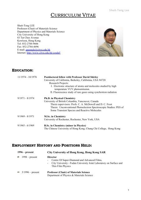
Shuit-Tong Lee<br />
Shuit-Tong LEE<br />
Professor (Chair) of Materials Science<br />
Department of Physics and Materials Science<br />
City University of Hong Kong<br />
83 Tat Chee Avenue<br />
Kowloon, Hong Kong<br />
Tel: 852-2788-9606<br />
Fax: 852-2784-4696<br />
E-mail: apannale@cityu.edu.hk<br />
Internet: http://www.cityu.edu.hk/cosdaf/<br />
EDUCATION:<br />
11/1974 - 10/1976 Postdoctoral fellow with Professor David Shirley<br />
University of California, Berkeley, California, USA 94720<br />
Research Projects:<br />
I. Electronic structure of atoms and molecules studied by high<br />
temperature VUV photoemission.<br />
II. Fluorescence study of rare gases using synchrotron radiation<br />
9/1971 - 8/1974 Ph.D. in Physical Chemistry<br />
University of British Columbia, Vancouver, Canada<br />
Thesis supervisors: Profs. C. A. McDowell and D. C. Frost<br />
Thesis: Unconventional Photoelectron Spectroscopic Studies: PES of<br />
Some Transient Species and Reactive Molecules<br />
9/1969 - 8/1971 M.Sc. in Chemistry<br />
University of Rochester, Rochester, New York, USA<br />
9/1965 - 6/1969 B.Sc. in Chemistry (minor in Physics)<br />
The Chinese University of Hong Kong, Chung Chi College, Hong Kong<br />
EMPLOYMENT HISTORY AND POSITIONS HELD:<br />
1996 – present City University of Hong Kong, Hong Kong SAR<br />
1998 – present Director<br />
- Centre Of Super-Diamond and Advanced Films,<br />
- City University - Fudan University Joint Laboratory on Surface and<br />
Thin Film Physics<br />
3/1996 – present Professor (Chair) of Materials Science<br />
Department of Physics & Materials Science<br />
1
3/1995 - 3/1996 Associate Professor<br />
Department of Physics & Materials Science<br />
Shuit-Tong Lee<br />
10/1994 - 3/1995 Senior Lecturer<br />
Department of Physics & Materials Science<br />
1976 – 1993 Eastman Kodak Company, Rochester, New York, USA<br />
6/1986 - 9/1993 Group Leader, Ion Beam Technology group (4 Ph.D.’s, 2 Technicians)<br />
Analytical Sciences Division, USA<br />
6/1983 - 6/1986 Group Leader, Surface Science Group (4 Ph.D.’s, 3 M.Sc.’s 2<br />
Technicians)<br />
12/1980 - 6/1985 Senior Research Scientist, Corporate Research Labs.<br />
11/1976 - 10/1980 Research Scientist, Corporate Research Labs.<br />
RESEARCH INTERESTS:<br />
Nanoscience and nanotechnology, organic electroluminescence and optoelectronics, organic emitting diode<br />
(OLED) / Polymeric emitting diode (PLED) display technology, thin films and super-hard coatings, surface<br />
science and modification applied to organics, polymers, interfaces, nanomaterials, and thin films<br />
AWARDS:<br />
--- National Natural Science Award (2 nd Class Award)<br />
State Council of the People's Republic of China<br />
2002 National Natural Science Award (2 nd Class Award)<br />
State Council of the People's Republic of China<br />
2002 The Croucher Award - Senior Research Fellowship<br />
The Croucher Foundation, Hong Kong SAR<br />
2001 Humboldt Research Award<br />
Alexander von Humboldt Foundation, Germany<br />
1999 Shenyang Science & Technology Award (1 st Class Award )<br />
Shenyang Government of Science & Technology, Shenyang<br />
PROFESSIONAL ROLES:<br />
Directorship:<br />
2001 – present Director<br />
Nano-organic Photoelectronic Laboratory<br />
Technical Institute of Physics and Chemistry, CAS, Beijing<br />
2
Shuit-Tong Lee<br />
Editorship of International Refereed Journals:<br />
Overseas Journals:<br />
2004 – present Regional Editor for Asia, Physica Status Solidi A, B & C (IF:0.95-0.99)<br />
Publisher: Elsevier Science, Europe<br />
1995 – present Associate Editor, Diamond and Related Materials (IF: 1.87)<br />
Publisher: Elsevier Science, Europe<br />
2003 – present Editorial Board, Applied Physics Letters (IF: 4.05)<br />
Publisher: The American Institute of Physics, USA<br />
2003 – present Editorial Board, Journal of Applied Physics (IF: 2.17)<br />
Publisher: The American Institute of Physics, USA<br />
2000 – present Advisory Editorial Board, Advanced Functional Materials (IF: 4.80)<br />
Publisher: WILEY-VCH Verlag GmbH & Co. KGaA, Germany<br />
2003 – present Honorary Editorial Board, Applied Nanoscience<br />
Publisher: Open Mind Journals Ltd., New Zealand<br />
2005 Guest Editor, Nanotechnology (Special Issue in 2005)<br />
Publisher: Institute of Physics Publishing, UK<br />
Mainland Journals:<br />
2002 – present<br />
(till 2005)<br />
Editorial Board, Journal of Materials Science & Technology (SCI listed<br />
journal)<br />
1999 – present Editorial Board, New Carbon Materials<br />
2004 – present Editorial Board, Chinese Physical Society – Journal of Luminescence<br />
2004 – present Editorial Board, Nanotechnology & Precision Engineering<br />
Research Committee:<br />
2002 – present<br />
(till 2005)<br />
863 Specialist<br />
863 High Tech Research and Development Program in “High-Resolution<br />
Panel Display Technology”<br />
Ministry of Science and Technology, P.R. China<br />
2004 – present RGC Panel Member<br />
Physical Sciences Panel of the Research Grants Council (RGC)<br />
Hong Kong SAR<br />
2002 – 2003 Member of the Evaluation Panel<br />
Department of Engineering & Material Science<br />
National Natural Science Foundation of China<br />
2001 – present Member of Reviewing Panel Committee,<br />
Research proposal for nanoscience and nanotechnology,<br />
National Science Council, Taiwan<br />
Reviewer for research proposals / journals papers:<br />
Research Proposal:<br />
3
1987 – 1993 The US National Science Foundation<br />
1987 – 1993 The US Naval Research Laboratory<br />
1987 – 1993 The US Air Force Office<br />
2003 – present National Science Science Award<br />
State Council of the People's Republic of China<br />
1995 – present RGC of Hong Kong<br />
Shuit-Tong Lee<br />
International refereed Journals:<br />
Science<br />
Physical Review Letters<br />
Journal of American Chemical Society<br />
Advanced Materials<br />
Advanced Functional Materials<br />
Journal of Applied Physics<br />
Applied Physics Letter<br />
Journal of Physical Chemistry<br />
Nano Letters<br />
Physical Review B<br />
Journal Vacuum Science & Technology<br />
Diamond and Related Materials<br />
Journal of Chemical Physics<br />
Chemical Physics Letters<br />
Honorary Position - Advisory/ Guest Professor<br />
1998 – 2001 Institute of Physics, CAS, Beijing<br />
2000 – 2002 Peking University, Beijing<br />
2000 – present Technical Institute of Physics and Chemistry, CAS, Beijing<br />
1998 – present Fudan University, Shanghai<br />
2002 – present Shanghai Jiao Tong University, Shanghai<br />
2000 – present Jilin University, Changchun<br />
2000 – present Zhejiang University, Hangzhou<br />
1996 – present Hunan University, Hunan<br />
1995 – present Dalian University of Science and Technology, Dalian<br />
2003 – present Changchun Institute of Optics and Fine Mechanics, Changchun<br />
2002 – present Xian Institute of Technology, Xian<br />
Government Committees & Community Services<br />
2003 – present Review Committee Member<br />
Department of Chemistry, National Taiwan University<br />
4
Shuit-Tong Lee<br />
2003 – present Member of the Solicitors Disciplinary Tribunal Panel<br />
Court of Final Appeal, Hong Kong SAR<br />
2003 – present Member<br />
Municipal Services Appeals Board, The Government of HKSAR<br />
- present Chairman<br />
Anna Leung-yee Tang Scholarship Fund<br />
1997 – present Member of the Executive Committee<br />
HK Student Aid Society, Hong Kong SAR<br />
1998 – present Adjudicator<br />
Registration of Persons Tribunal, The Government of HKSAR<br />
ACADEMIC RESEARCH EXPERIENCE:<br />
Principal and Co-Principal Investigator of the following funded projects:<br />
S.T. Lee is the Principal Investigator of over 30 research projects, including Innovation and Technology Fund,<br />
RGC and Industrial projects with total sum over HK$46M last 10 years.<br />
Principal investigator:<br />
1. Band Gap Engineering in II-VI Single-Crystal Nanoribbons for Lasing Applications in the<br />
Visible-UV Region, Competitive Earmarked Research Grant, 2006-2008 (HK$ 532,344)<br />
2. Single Nanostructure Optical and Lasing Characterization, CityU Strategic Research Grant, 2005-<br />
2008 (HK$ 180,000)<br />
3. Science and Technology of Silicon Nanowire (Renewal), RGC Central Allocation, Grant 2005-2008<br />
(HK$3,450,000)<br />
4. Controlled Synthesis and Optical Properties of II-VI Semiconductor Nanostructures, CAS -<br />
Croucher Funding Scheme for Joint Laboratories, 2004-2007 (HK$ 800,000)<br />
5. An alternative to Indium-Tin-Oxide (ITO) Transparent Conducting Electrode--with Emphasis on<br />
Aluminum-doped Zinc Oxide (AZO) Electrode, Contract Research Project, 2005-2006 (HK$850,000)<br />
6. Organic Light Emitting Diode, Contract Research Project, 2005-2006 (HK$2,000,000)<br />
7. Synthesis and Characterization of ZnS Nanowires and Nanoribbons, Competitive Earmarked<br />
Research Grant, 2004-2007 (HK$ 455,800)<br />
8. Organic Light Emitting Diode, Contract Research Project, 2004-2005 (HK$900,000)<br />
9. Surface States of Semiconducting Nanowires, Germany/HK Joint Research Scheme, 2005 (HK$<br />
29,800)<br />
10. Optical and Lasing Properties of Zinc Oxide Nanostructure, Competitive Earmarked Research<br />
Grant, 2003-2006 (HK$ 705,408)<br />
11. Group Research in "Organic Electroluminescence" – Renewal funding, RGC Central Allocation,<br />
Grant 2003-2005 (HK$1,800,000)<br />
12. Science and Technology of Silicon Nanowire, RGC Central Allocation, Grant 2002-2004<br />
(HK$1,680,000)<br />
13. Organic Light Emitting Displays, Contract Research Project – Shenzhen SAST Enterprise, 2003-<br />
2004 (HK$ 1,400,000)<br />
14. Fundamentals of Nano Devices, Chinese Academy of Sciences, P.R. China, Grant 2002-2006 (RMB$<br />
1,000,000)<br />
15. Applied R&D in Organic Light Emitting Materials, Chinese Academy of Sciences, P.R. China,<br />
Grant 2002-2004 (RMB$ 1,500,000)<br />
16. Structural and Electrical Characterization of Si Nanowires, Competitive Earmarked Research<br />
Grant, 2001-2003 (HK$ 391,160)<br />
5
Shuit-Tong Lee<br />
17. Organic Electroluminescent Flat-panels for Hong Kong, Innovation & Technology Fund, 2001-<br />
2003 (HK$ 5,810,000)<br />
18. Controlled Growth of Intramolecular Junction Structures in Carbon Nanotubes, CityU SRG<br />
Grant 2002-2004 (HK$ 200,000)<br />
19. Study of Nucleation and Growth of Carbon Nanotubes, CityU SRG Grant 2002-2004 (HK$ 228,272)<br />
20. Synthesis of Ordered Organic Materials and Their Applications in Organic Light Emitting<br />
Diodes and Laser Devices, NSFC/RGC Grant 2001-2004 (HK$590,000)<br />
21. Organic Light Emitting Diodes, 863 Project-Mainland, P.R. China (RMB$1,600,000) (2000-2003)<br />
22. International Conference on New Diamond Science and Technology, General Support Fund,<br />
Innovation and Technology Commission (HK$200,000) (2000)<br />
23. Ion Beam Synthesis of Nanoscale Materials, Germany/HK Joint Research Scheme 2000-2002<br />
($30,000)<br />
24. Studies of Electrode Modifications for Use with Conjugated Polymer Light-emitting Devices,<br />
UK/HK Joint Research Scheme 2000-2001 ($73,200)<br />
25. Industrial Support Fund: Establishment of Organic Electroluminescent Display Technology in<br />
Hong Kong ($17,024,000) ($14,924,000 from Industry Department, $800,000 from COTCO, $800,000<br />
from Varitronix, $500,000 from University Matching Fund) (1998-2001)<br />
26. Group Research into Organic Electroluminescence, RGC Central Allocation Scheme ($4,200,000)<br />
(1998-2001)<br />
27. Growth of Diamond on Fe-based Materials and Characterization of Interfacial Structure, RGC<br />
Competitive Earmarked Research Grant 1998-2000 ($480,000)<br />
28. Atomic Structure of Diamond Surfaces, Competitive Earmarked Research Grant ($405,000) (1999 -<br />
2000)<br />
29. Applications of Diamond-like Carbon(DLC) and Nitrogen-doped Carbon (CNx) in Organic<br />
Light-emitting Diode, Research Grants Council/Competitive Earmarked Research Grant ($545,000)<br />
(1998 – 2000)<br />
30. Interface Structure and Engineering in Organic Light Emitting Diodes, Research Grants Council<br />
of the Universities Grants Committee of Hong Kong ($958,100). (6/1997 - 5/1999)<br />
31. Failure Analysis and Process Evaluation of AMR and Spin-valve GMR heads, Donation Projects<br />
($622,560) (4/1998 – 4/2002)<br />
32. Diamond Heteroepitaxy of Silicon, Research Grants Council of the Universities Grants Committee of<br />
Hong Kong ($470,600) (9/1996 - 8/1998)<br />
33. A High Resolution Electron Energy Loss Spectrometer (HREELS), RGC Central Allocation<br />
($3,700,000) (1996-2000)<br />
34. Surface and Negative Electron Affinity Properties of Diamond, Research Grants Council of the<br />
Universities Grants Committee of Hong Kong ($711,000) (12/1995 - 11/1997)<br />
35. Characterization of Diamond and Related Thin Films by Convergent Beam Electron Microscopy,<br />
UK/Hong Kong Joint Research Scheme ($77,000) (12/1996 - 11/1997)<br />
36. Ion Beam Approach to Heteroepitaxial Nucleation and Growth of Diamond, City University of<br />
Hong Kong ($350,000) (8/1995 - 5/1997)<br />
37. Mechanistic Study of Negative Electron Affinity of Diamond, City University of Hong Kong<br />
($370,000) (Completed with Outstanding Achievement) (1995 - 1997)<br />
Co-Principal investigator / Co-investigator:<br />
S.T. Lee is the Co-Investigator of over 20 research projects, including Innovation and Technology Fund,<br />
and RGC projects with total sum over HK$20M last 10 years.<br />
1. Synthesis of Stress-free Vubic Boron Nitride Films via Electron-bombardment-enhanced<br />
Surface Reactions, RGC Competitive Earmarked Research Grant, 2006-2008 (HK$ 680,037)<br />
2. Interface Engineering of Organic Heterojunctions, RGC Competitive Earmarked Research Grant,<br />
2006-2007 (HK$ 413,324)<br />
3. Facility for Single Nano-object Characterization (Raman/NSOM/AFM), RGC Central Allocation<br />
Equipment Grant, 2004-2005 (HK$2,700,000)<br />
4. Nano-structuring of Diamond Films for Field Electron Emission Applications, RGC Competitive<br />
Earmarked Research Grant, 2004-2006 (HK$ 700,394)<br />
6
Shuit-Tong Lee<br />
5. Carrier Injection Barrier and Interface Dipole at Metal/Organic Interface, RGC Competitive<br />
Earmarked Research Grant, 2004-2007 (HK$ 866,877)<br />
6. Diamond Coatings for Hong Kong Manufacturing Industry, Innovation and Technology Support<br />
Fund ($9,860,000) (2000-2003)<br />
7. Lowering Operating Voltage of Organic Light-emitting Diodes by Improving Electron<br />
Transport Capability, RGC Competitive Earmarked Research Grant ($520,000) (2000-2002)<br />
8. Electrode Modification and Interface Optimization of Polymer Light Emitting Diodes, RGC<br />
Competitive Earmarked Research Grant ($790,000) (2000-2002)<br />
9. Ion Beam Nucleation of Diamond, RGC Competitive Earmarked Research Grant, ($778,817) (2000-<br />
2002)<br />
10. Co-operative Research in Active Matrix Organic Light Emitting Diode Displays, ($1,080,000)<br />
RGC Funding for Co-operative Research Centres (2000-2002)<br />
11. Fabrication of Solid State Organic Lasers for Short Wavelength Applications, RGC Competitive<br />
Earmarked Research Grant (575,000) (1999-2001)<br />
12. Degradation Mechanism of Organic Electroluminescent Devices, RGC Competitive Earmarked<br />
Research Grant ($986,000) (1999-2002)<br />
13. Synthesis and Characterization of Semiconductor Nanowires, RGC Competitive Earmarked<br />
Research Grant ($405,000) (1999-2002)<br />
14. Growth and Characterization of Semiconductor Nanocomposites, RGC Competitive Earmarked<br />
Research Grant ($420,000) (1999-2002)<br />
15. Study of Nano Materials Using Synchrotron Radiation, CityU Strategic Research Grant (7001112,<br />
On-going)<br />
16. Towards Design of Luminescent and Electron-transport Organic Molecules for Light Emitting<br />
Device, CityU Strategic Research Grant<br />
17. Synthesis Towards Single Crystal Diamond Film, RGC Competitive Earmarked Research Grant,<br />
($560,000) (1998-2000)<br />
18. Heteroepitaxial Growth of Beta-silicon Carbide on Silicon, RGC Competitive Earmarked Research<br />
Grant ($500,000) (1998-2000)<br />
19. Surface Vibrational Spectroscopy: A High Resolution Electron Energy Loss Spectrometer, RGC<br />
Central Allocation Scheme for $2.4 million (3/1996)<br />
20. Synthesis and Characterization of Cubic Boron Nitride, Research Grants Council of the<br />
Universities Grants Committee of Hong Kong ($672,100) (6/1997 - 5/1999)<br />
21. Metallization of Diamond for Thermal Management, Research Grants Council of the Universities<br />
Grants Committee of Hong Kong ($360,000) (6/1997 - 5/1999)<br />
22. Transmission Electron Microscopy Study of Phase Transition and Defects in Octagonal<br />
Quasicrystals, City University of Hong Kong ($390,000) (7/1997 - 6/1999)<br />
23. Modification of Diamond by Metal Ion Beam Enhanced Deposition and Its Applications, City<br />
University of Hong Kong ($350,000) (8/1996 - 7/1998)<br />
24. Industrial Applications of Diamond-like Carbon (DLC) to Plastics, Hong Kong Government<br />
Industry Department ($986,000) (1995 - 1997)<br />
25. Growth and Characterization of Carbon Nitride Films, Research Grants Council of the<br />
Universities Grants Committee of Hong Kong ($470,600) (1995 - 1997)<br />
26. Study of Thermal Properties of Diamond Materials by Holographic Interferometry, City<br />
University of Hong Kong ($350,000) (12/1994 - 1996)<br />
Attracted and brought to City University of Hong Kong equipment valued at ~HK$ 6 million from<br />
Eastman Kodak Company (1994 - 1995)<br />
7
RESEARCH STUDENTS:<br />
Shuit-Tong Lee<br />
PhD graduates / students:<br />
4 PhD. in progress Wei Wei CHEN, Siew Ling CHEW, Yanqing LI, Ho TANG<br />
2005 1 graduate: F. Chi Kan AU<br />
2004 4 graduates: Wing Kwong WONG, Suidong WANG, Fu Long WONG, Yuen<br />
YAO<br />
2003 3 graduates: Baoxiu MI, Man-Keung FUNG, Chi Pui LI<br />
2002 2 graduates: Xin Tai ZHOU, Samuel Cheng Hao LEE<br />
2000 1 graduate: Zhi Qiang GAO<br />
1999 3 graduates: Kai-Wai WONG, Xiaosong SUN, Chao SUN<br />
MPhil graduates / students:<br />
4 MPhil in progress Kai Chun LAU, Tsz Yan LUI, Chin Wai LAW, Ting Fung CHUNG<br />
2004 4 graduates: Junxian DING, Xiang DONG, Chunya GENG, Chung On POON<br />
2001 1 graduate: Wai Yuen LAI<br />
1999 2 graduates: Man-Keung FUNG, Lai-Man HUNG<br />
1998 1 graduate: Hin-Koon WOO<br />
CONFERENCE ORGANIZED:<br />
Chairman / Organizing Committee Member :<br />
2006 Organizing Chair<br />
The 6th International Conference on Electroluminescence of Molecular Materials<br />
and Related Phenomena (ICEL-6), Hong Kong SAR, 7-10 August 2006.<br />
2005 Member of Organizing Committee<br />
The 10th International Conference on New Diamond Science and Technology<br />
(ICNDST-10), Japan, 11-14 May 2005<br />
2004 Chairman<br />
Inter-Pacific Workshop on Nanoscience and Nanotechnology<br />
City University of Hong Kong, Hong Kong SAR, 22-24 November 2004<br />
2003 Organizing Committee Member<br />
Symposium on “Advances in Carbon-based Materials”, The 5th International<br />
Meeting of Pacific RimCeramic Societies, 29 September – 5 October 2003<br />
2002 Chairman<br />
The 2 nd Cross-Strait Workshop on “Nano Science and Technology<br />
City University of Hong Kong, Hong Kong SAR, 9-11 December 2002<br />
Organizing Committee Member<br />
Symposium G, “Advanced Materials and Devices for Large Area Electronics”,<br />
IUMRS-ICEM2002, Xian, China, 10-14 July 2002<br />
8
Shuit-Tong Lee<br />
2001 Organizing Committee Member<br />
Symposium G, “Plastic Electronics – Materials & Devices”, International<br />
Conference on Materials for Advanced Technologies, Singapore, 1-6 July 2001<br />
2000 Chairman<br />
The 7 th International Conference of New Diamond Science and Technology<br />
(ICNDST-7), City University of Hong Kong, Hong Kong SAR, 24-28 July, 2000.<br />
Chairman<br />
The International Union of Materials Research Societies – 6 th International<br />
Conference in Asia (IUMRS-ICA2000),<br />
City University of Hong Kong, 24-28 July, 2000<br />
1999 Chairman<br />
Asia Pacific Symposium on Organic Electroluminescent Materials and Displays,<br />
City University of Hong Kong, Hong Kong SAR, 8-11 June, 1999<br />
Organizing Committee Member<br />
Symposium E, “Diamond & Related Materials”, IUMRS 1999,<br />
Beijing, China, 13-18 June, 1999<br />
Organizing Committee Member<br />
The International Conference on Surface Modification of Metals by Ion Beams<br />
(SMMIB), Beijing, China, 19-24 Sept. 1999<br />
International Committee Member:<br />
2006 Member of International Advisory Committee<br />
ECI Conference - Innovative Nanoscale Approach to Dynamic Studies of Materials,<br />
Japan, 9-14 January 2006<br />
2005 Member of International Committee<br />
The 16 th European Conference on Diamond, Diamond-Like Materials, Carbon<br />
Nanotubes, Nitrides & Silicon Carbide<br />
France, 11-16 September 2005<br />
Member of International Advisory Committee<br />
Applied Diamond Conference on Nanocarbon 2005, Argonne, USA, 15-19 May,<br />
2005<br />
Member of International Committee<br />
The 5th International Conference on Electroluminescence of Molecular Materials<br />
and Related Phenomena (ICEL-5), USA, 17-27 January 2005<br />
Member of International Committee<br />
The First International Conference on One-Dimensional Nanomaterials (ICON)<br />
Taipei, 9-13 January 2005<br />
2004 Member of International Scientific Steering Committee<br />
The 15 th European Conference on Diamond, Diamond-Like Materials, Carbon<br />
Nanotubes, Nitrides & Silicon Carbide<br />
Italy, 12-17 September 2004<br />
Member of Program Committee<br />
The 9th International Conference on New Diamond Science and Technology<br />
9
(ICNDST-9), Japan, 26-29 March 2004<br />
Shuit-Tong Lee<br />
Member of International Advisory Committee<br />
Conference on Dynamics of Disordered Materials on the Nanometer Scale<br />
Vietnam , 22-27 February 2004<br />
2003 Member of International Scientific Steering Committee<br />
The 14 th European Conference on Diamond, Diamond-Like Materials, Carbon<br />
Nanotubes, Nitrides & Silicon Carbide<br />
Austria, 7-12 September 2003<br />
2002 Member of International Scientific Steering Committee<br />
The 13 th European Conference on Diamond, Diamond-Like Materials, Carbon<br />
Nanotubes, Nitrides & Silicon Carbide<br />
Spain, 8-13 September 2002<br />
Member of Program Committee<br />
The 8th International Conference on New Diamond Science and Technology<br />
(ICNDST-8), Australia, 21-26 July 2002<br />
PATENTS:<br />
1. K. Y. Ko, S. Chen, and S.T. Lee, "Isolation region in a group III-V semiconductor device and method of<br />
making the same", US Patent No. 5,399,900, March 21, 1995.<br />
2. L.S. Hung, C.W. Tang and S.T. Lee, "Conductive electron injector for light-emitting diodes", US patent<br />
no. 5,608,287, March 4, 1997.<br />
3. S.T. Lee, C.S. Lee, I. Bello, Y.W. Lam and H. K. Woo, "Method of heteroepitaxial growth of beta<br />
silicon carbide on silicon", US Patent No.5,879,450, March 9, 1999.<br />
4. S.T. Lee, C.S. Lee, Z.D. Lin and Y.W. Lam, "Deposition method for heteroepitaxial diamond", US<br />
Patent No. 6,063,187, May 16, 2000.<br />
5. S.T. Lee, C.S. Lee, N. Wang, I. Bello, C.H. L. Lai, X.T. Zhou and F.C.K. Au, "Method for growing<br />
beta-silicon carbide nanorods, and preparation of patterned field-emitters by chemical vapor deposition<br />
(CVD)", US Patent no. 6,221,154, April 2001.<br />
6. S. T. Lee, N. Wang, C. S. Lee and I. Bello, "Growth method for silicon nanowires and nanoparticle<br />
chains from silicon monoxide", US Patent no. 6,313,015, November 6 2001.<br />
7. S. T. Lee, Z. B. Deng and W. A. Gambling, "Organic electroluminescent device with improved hole<br />
injecting structure", US Patent No. 6,351,067, 26 February 2002.<br />
8. S. T. Lee, C. S. Lee and Z. Q. Gao, "White and colored organic electroluminescent devices using single<br />
emitting material by novel color change technique", US Patent no. 6,521,360, 18 February 2003.<br />
9. S.T. Lee, C.S. Lee, L.S. Hung, M.X. Mi, Z.Q. Gao, "Organic electroluminescent elements", US Patent<br />
no. 6,613,458, 2 September 2003.<br />
10. S.T. Lee, I. Bello, C.S. Lee, Q. Li, N.G. Shang, "Large area silicon cone arrays fabrication and cone<br />
based nanostructure modification", US Patent No. 6,761,803, 13 July 2004.<br />
11. S. T. Lee, C. S. Lee, P. F. Wang, Z. Y. Xie, “Electroluminescent Devices”, US Patent No. 6,833,202,<br />
21 December 2004.<br />
12. S.T. Lee, C.S. Lee, P.F. Wang, Z.Y. Xie, “Organic electroluminescent devices using<br />
pyrazolo[3,4b]quinoxaline derivatives”, US Patent No. 6,861,162, 1 March 2005.<br />
13. S.T. Lee, W.J. Zhang, I. Bello, C.Y. Chan, “Fabrication of Single Crystal Diamond Tips and their<br />
Arrays”, US Patent No. 6,902,716, 7 June 2005.<br />
14. S.T. Lee, X. Jiang, C.S. Lee, F.L. Wong, “High-quality aluminum-doped zinc oxide layer als transparent<br />
conductive electrode for organic light-emitting devices”, US Patent 6,917,158 B2, 12 July 2005.<br />
10
Shuit-Tong Lee<br />
15. S. T. Lee, C. P. Li, X. H. Sun, N. B. Wong, C. S. Lee, Boon K. Teo, “Room temperature solutions<br />
synthesis of multiwalled carbon nanostructures”, US Patent application no. 10/273,242.<br />
16. I. Bello, W.J. Zhang, S.T. Lee, “Cubic boron nitride/ diamond composite (cBND) layers”, US Patent<br />
application no. 10/366,880, 14 February 2003.<br />
17. S.T. Lee, C.S. Lee, P.F. Wang, B.X. Mi, “Electroluminescent devices”, US Patent application no.<br />
10/357, 616 (March 2003).<br />
18. S.T. Lee, C.S. Lee, L.S. Hung, B.X. Mi, Z.Q. Gao, “Red-emitting organic electroluminescent elements”,<br />
US Patent application No. 10/391,265, filed on 18 March 03.<br />
19. S.T. Lee, C.S. Lee, S.L. Lai, M.Y. Chan, “Organic electroluminescent devices formed with rare earth<br />
metal containing cathode”, US Patent application no. 10/656,641 (pending).<br />
20. C.S. Lee, S.T. Lee, Y. Lifshitz, S.W. Tong, “Ultraviolet light-illuminated fluorocarbon films for OLED<br />
applications”, US Patent application no. 11/124,686, filed on 9 May 05.<br />
21. S.T. Lee, C.S. Lee, B.X. Mi, P.F. Wang, “Improvement in red-emitting electrophosphorecent Devices”,<br />
US Patent application (pending), submitted to lawyer for filing.<br />
22. S.T. Lee, C.S. Lee, P.F. Wang, Z.Y. Xie, “Organic electroluminescent device using phenazine dyes –<br />
neutral red derivatives”, US Patent application (pending).<br />
23. S.T. Lee, C.S. Lee, J.Y. Li, “Organic light-emitting devices containing morphologically stable hole<br />
transporting materials”, US Patent application (pending).<br />
BOOK CHAPTERS:<br />
1. M.K. Fung, C.S. Lee, S.T. Lee, “Metal/Polymer Interface Studies for Organic Light-Emitting<br />
Devices” in Electroluminescence — From Synthesis to Devices, (in press) edited by K. Müllen, U.<br />
Scherf, Publisher: Wiley-VCH Verlag GmbH & Co. KGaA.<br />
2. S.T. Lee, R. Q. Zhang and Y. Lifshitz, “Oxide-assisted growth of silicon and related nanowires:<br />
growth mechanism, structure and properties”, in “The Chemistry of Nanomaterials”, (2004), edited<br />
by C.N.R. Rao, A. Müller, A.K. Cheetham, Wiley-VCH Verlag GmbH & Co. KGaA.<br />
3. S.T. Lee, R.Q. Zhang and Y. Lifshitz, “Silicon-based nanowires” in “Nanowires and Nanobelts –<br />
Materials, Properties and Devices, Metal and Semicondutor Nanowires” (Vol. 1), (2003) edited by<br />
Z.L. Wang, Kluwer Academic Publisher.<br />
4. L.S. Liao, C.S. Lee, S.T. Lee, M. Inbasekaran and W.W. Wu, "Metal/polyfluorene interface and<br />
surface: structures and stability" in "Conjugated Polymer and Molecular Interfaces: Science and<br />
Technology for Photonic and Optoelectronic Applications", (2002) edited by W.R. Salaneck, K. Seki,<br />
A. Kahn and J.J. Pireaux, Marcel Dekker.<br />
5. J. F. Hamilton, G. Apai, S.T. Lee, and M. G. Mason, “Binding energies, bond length charges, and<br />
band structure formation in small cluster”, Growth and Properties of Metal Clusters (1980), ed. by J.<br />
Bourdon.<br />
6. D.A. Shirley, S.T. Lee, S. Suzer, R.L. Martin, E. Matthias, and R.A. Rosenberg, “Electron<br />
correlation in atoms from photoelectron spectroscopy”, Atomic Physics 5 (1977), Plenum Publishing<br />
Corporation.<br />
11
JOURNAL ARTICLES:<br />
Shuit-Tong Lee<br />
Over 480 papers published in internationally refereed journals, including three papers in Science , two<br />
papers in Nature and several invited review articles.<br />
Publications in Science & Nature:<br />
1. D.D.D. Ma, C.S. Lee, F.C.K. Au, S.Y. Tong, S.T. Lee, “Small diameter silicon<br />
nanowire surface”, Science 299, 1874-1877 (2003). (March 2003)<br />
The nanowire images of the paper were featured as the coverpage of the Science<br />
(March 2003).<br />
2. S.T. Lee, Y. Lifshitz, “The road to diamond wafers“, Nature 424, 500 (2003).<br />
3. Y. Lifshitz, Th. Kohler, Th. Frauenheim, I. Guzmann, A. Hoffman, R.Q. Zhang, X.T.<br />
Zhou, S.T. Lee, “The mechanism of diamond nucleation from energetic species”,<br />
Science 297, 1531 (2002). (August 2002)<br />
4. Y. Lifshitz, X. F. Duan, N. G. Shang,Q. Li, L. Wan, I. Bello, S. T. Lee, "Epitaxial diamond polytypes on<br />
silicon", Nature 412, 404 (2001).<br />
5. S.T. Lee, H.Y. Peng, X.T. Zhou, N. Wang, C.S. Lee, I. Bello, Y. Lifshitz, "A Nucleation site and<br />
mechanism leading to epitaxial growth of diamond films", Science 287 104-106, (2000).<br />
Invited papers / invited review papers:<br />
6. Y. Zhang and S. T. Lee, “Diamond Crystals, Growth of” Encyclopedia of Materials: Science and<br />
Technology, 2113-2118 (2004).<br />
7. R.Q. Zhang, Y. Lifshitz, S.T. Lee, “Oxide-assisted growth of semiconducting nanowires”, Adv. Mater. 15,<br />
635-640 (2003).<br />
8. Z. R. Hong, O. Lengyel, C. S. Lee and S. T. Lee, “A mechanistic study of exciplex formation and efficient<br />
red light-emitting devices based on rare earth complexes”, Organic Electronics 4, 149-154. (2003)<br />
9. S.T. Lee, N. Wang, Y.F. Zhang and Y.H. Tang, "Oxide-Assisted Semiconductor Nanowire Growth", MRS<br />
Bulletin August 36-42 (1999).<br />
10. S.T. Lee, Z.D. Lin and X. Jiang, "CVD diamond films: nucleation and growth", Materials Science &<br />
Engineering R. 25, 123-154 (Aug.1999).<br />
Nanomaterials & Nanotechnology<br />
Publication in 2005 (Nanomaterials & Nanotechnology)<br />
11. H. Wang, X.H. Zhang, X.M. Meng, S.M. Zhou, S.K. Wu, W.S. Shi, S.T. Lee, “Bulk preparation of Si–<br />
SiOx hierarchical structures: high-density radially oriented amorphous silica nanowires on a singlecrystal<br />
silicon nanocore”, Angewandte Chemie International Edition (in press, 2005).<br />
12. Y.K. Liu, J.A. Zapien, Y.Y. Shen, C.Y. Geng, C.S. Lee, S.T. Lee, “Wavelength-control lasing in<br />
Zn X Cd 1-X S single-crystal nanoribbons”, Adv. Mater. 17, 1372-1377 (2005). June 2005<br />
13. M.W. Shao, Y.Y. Shan, N.B. Wong, S.T. Lee, “Silicon nanowire sensors for bioanalytical applications:<br />
glucose and hydrogen peroxide detection”, Adv. Funct. Mater. 15, 1478-1482 (2005). (September<br />
2005).<br />
14. X. Fan, X.M. Meng, Z.H. Zhang, S.K. Wu, S.T. Lee, “Formation of ZnS/SiO2 nanocables”, Appl. Phys.<br />
Lett. 86, 173111 (2005). (April 2005)<br />
15. W.W. Chen, C.H. Tzang, J.X. Tang M.S. Yang, S.T. Lee, “Covalently linked deoxyribonucleic acid<br />
with multiwall carbon nanotubes: Synthesis and characterization”, Appl. Phys. Lett. 86, 103114 (2005).<br />
(March 2005)<br />
16. J.J. Qiao, X.H. Zhang, X.M. Meng, S.M. Zhou, S.K. Wu, S.T. Lee, “Morphology-controllable<br />
preparation of 1D poly(vinyl pyrrolidone nanostructured arrays”, Nanotechnology 16, 433 – 436 (2005).<br />
(April 2005).<br />
17. W.W. Chen, X. H. Sun, S. D. Wang, S. T. Lee, and Boon K. Teo, “Etching Behavior of silicon<br />
nanowires with HF and NH4F and surface characterization by attenuated total reflection Fourier<br />
12
Shuit-Tong Lee<br />
transform infrared spectroscopy: Similarities and differences between one-dimensional and twodimensional<br />
silicon surfaces”, J Phys. Chem. B 109, 10871-10879 (2005). June 2005<br />
18. M.W. Zhao, Y.Y. Xia, F. Li, R.Q. Zhang, S.T. Lee, “Strain energy and electronic structures of silicon<br />
carbide nanotubes: Density functional calculations”, Phys. Rev. B. 71, 085312 (2005). (February 2005)<br />
19. X. T. Zhou, T. K. Sham, Y. Y. Shan, X. F. Duan, S. T. Lee, and R. A. Rosenberg, “One-dimensional<br />
zigzag gallium nitride nanostructures”, J. Appl. Phys. 97, 104315 (2005).<br />
20. W.K. Wong, C.S. Lee, and S.T. Lee, “Uniform-diameter, aligned carbon nanotubes from microwave<br />
plasma-enhanced chemical-vapor deposition”, J. Appl. Phys. 97, 084307 (1-6) (2005). April 2005<br />
21. K.Q. Peng, Y. Xu, Y. Wu, Y.J. Yan, S.T. Lee, J. Zhu, “Aligned single-crystalline Si nanowire arrays<br />
for photovoltaic applications”, Small (in press)<br />
22. J.Q. Hu, Y. Zhang, X.M. Meng, C.S. Lee, S.T. Lee, “Temperature-dependent growth of germanium<br />
oxide and silicon oxide based nanostructures, aligned silicon oxide nanowire assemblies, and silicon<br />
oxide microtubes”, Small 1, 429-438 (2005). April 2005<br />
23. Y. Yao, F.H. Li, S.T. Lee, “Oriented silicon nanowires on silicon substrates from oxide-assisted growth<br />
and gold catalysts”, Chem. Phys. Letts. 406, 381-385 (2005). (May 2005).<br />
24. X. M. Meng, N. G. Shang, C. S. Lee, I. Bello, S. T. Lee, “Fabrication and microstructures of Si<br />
composite nanocone arrays”, Phys. Stat. Sol. (a) (in press).<br />
25. S.M. Zhou, X.H. Zhang, X.M. Meng, S.K. Wu, S.T. Lee, “Synthesis and optical properties of Pb-doped<br />
ZnO nanowires”, Phys. Stat. Sol. (a) 202, 405–410 (2005).<br />
26. S.M. Zhou, X.H. Zhang, X.M. Meng, X. Fan, S.K. Wu, S.T. Lee, “Preparation and photoluminescence<br />
of Sc-doped ZnO nanowires”, Physica E 25, 587–591 (2005).<br />
27. S.M. Zhou, X.H. Zhang, X.M. Meng, X. Fan, S.T. Lee, S.K. Wu, “Sonochemical synthesis of mass<br />
single-crystal PbS nanobelts”, J Solid State Chem 178, 399–403 (2005).<br />
28. S.M. Zhou, X.M. Meng, X.H. Zhang, X. Fan, K. Zou, S.K. Wu, S.T. Lee, “Large-scale fabrication and<br />
characterization of Cd-doped ZnO nanocantilever arrays”, Micron 36, 55–59 (2005).<br />
29. M.W. Zhao, Y.Y. Xia, R.Q. Zhang, and S.T. Lee, “Manipulating the electronic structures of silicon<br />
carbide nanotubes by selected hydrogenation”, J. Chem. Phys. 122, 214707 (2005)<br />
Publications in 2004 (Nanomaterials & Nanotechnology)<br />
30. R. Q. Zhang, M. W. Zhao, and S. T. Lee, “Silicon Monoxide Clusters: The Favorable Precursors for<br />
Forming Silicon Nanostructures”, Phys. Rev. Lett. 93, 095503 (2004). (August 2004)<br />
31. S.M. Zhou, X.H. Zhang, X.M. Meng, K. Zou, X. Fan, S.K. Wu, S.T. Lee, “The<br />
fabrication and optical properties of highly crystalline ultra-long Cu-doped ZnO<br />
nanowires”, Nanotechnology 15, 1152-1155 (2004). (September 2004)<br />
Y. K. Liu, J. A. Zapien, C. Y. Geng, Y. Y. Shan, C. S. Lee, Y. Lifshitz, and S. T. Lee,<br />
“High-quality CdS nanoribbons with lasing cavity”, Appl. Phys. Lett. 85, 3241-3243<br />
(2004). (October 2004) - The nanoribbon images of the paper were featured as the<br />
coverpage of the Applied Physics Letters (Oct 2004).<br />
32. J. X. Ding, J. A. Zapien, W. W. Chen, Y. Lifshitz, S. T. Lee, and X. M. Meng,<br />
“ Lasing in ZnS nanowires grown on anodic aluminum oxide templates”, Appl. Phys. Lett. 85, 2361<br />
(2004). (September 2004)<br />
33. A. Baumer, M. Stutzmann, M. S. Brandt, F. C.K. Au, and S. T. Lee, “Paramagnetic defects of silicon<br />
nanowires”, Appl. Phys. Lett. 85, 943 (2004). (Aug 2004)<br />
34. C. P. Li, T. C. Wong, R. Q. Zhang, and S. T. Lee, “Response to ``Comment on `Gold nanowires from<br />
silicon nanowire templates' '' [ Appl. Phys. Lett., 692 (2004) ], Appl. Phys. Lett. 85, 693 (2004).<br />
35. J. A. Zapien, Y. Jiang, X. M. Meng, W. Chen, F. C. K. Au, Y. Lifshitz, and S. T. Lee, “Roomtemperature<br />
single nanoribbon lasers”, Appl. Phys. Lett. 84, 1189-1191 (2004). (February 2004)<br />
36. T. C. Wong, C. P. Li, R. Q. Zhang, and S. T. Lee, “Gold nanowires from silicon nanowire templates”,<br />
Appl. Phys. Lett. 84, 407-409 (2004). (February 2004)<br />
37. C. Geng, Y. Jiang, Y. Yao, X. Meng, J. A. Zapien, C. S. Lee, Y. Lifshitz, S. T. Lee, “Well-aligned ZnO<br />
nanowire arrays fabricated on silicon substrates”, Adv. Funct. Mater. 14, 589-594 (2004). (June 2004)<br />
38. R. Q. Zhang, Y. Q. Feng, S. T. Lee, C. L. Bai, “ Electrical transport and electronic delocalization of<br />
small fullerenes”, J. Phys. Chem. B. 108, 16636-16641 (2004). (October 2004)<br />
39. Y. Jiang, X. M. Meng, W. C. Yiu, J. Liu, J. X. Ding, C. S. Lee and S. T. Lee, “Zinc selenide<br />
nanoribbons and nanowires”, J. Phys. Chem. B. 108, 2784-2787 (2004).<br />
40. R.Q. Zhang, W.C. Lu, Y.L. Zhao, S.T. Lee, “On the stability of hydride configurations on silicon<br />
cluster surfaces: A first-principle theoretical study”, J. Phys. Chem. B. 108, 1967-1973 (2004).<br />
13
Shuit-Tong Lee<br />
41. X. H. Sun, N. B. Wong, C. P. Li, S. T. Lee, P. S. Kim, T. K. Sham, “Reductive self-assembling of Pd<br />
and Rh nanoparticles on silicon nanowire templates”, Chem. Mater. 16, 1143-1152. (March 2004)<br />
42. M.W. Zhao, R.Q. Zhang, and S.T. Lee, “Stable tetrahedral structure of the silica cluster (SiO2), Phys.<br />
Rev. B. 70, 205404 (2004)<br />
43. T. K. Sham, S. J. Naftel, P.-S. G. Kim, R. Sammynaiken, Y. H. Tang, I. Coulthard, A. Moewes, J. W.<br />
Freeland, Y.-F. Hu, and S. T. Lee “Electronic structure and optical properties of silicon nanowires: A<br />
study using x-ray excited optical luminescence and x-ray emission spectroscopy”, Phys. Rev. B. 70,<br />
045313 (2004)<br />
44. M. W. Zhao, R. Q. Zhang, and S. T. Lee, “Stable and extendable cage containing nanosize silica<br />
clusters based on three-membered rings”, Phys. Rev. B 69, 153403 (2004). (May 2004).<br />
45. X. H. Sun, N. B. Wong, C. P. Li, S. T. Lee, and T. K. Sham, “Chainlike silicon nanowires: Morphology,<br />
electronic structure and luminescence studies”, J. Appl. Phys. 96, 3447-3451 (2004). (September 2004).<br />
46. Y. Q. Feng, R. Q. Zhang, and S. T. Lee, “Simulation of gate-controlled Coulomb blockade in carbon<br />
nanotubes”, J. Appl. Phys. 95, 5729-5735 (2004). (May 2004).<br />
47. F. M. Kolb, H. Hofmeister, R. Scholz, M. Zacharias, U. Gosele, D. D. Ma, and S.-T. Lee, “Analysis of<br />
silicon nanowires grown by combining SiO evaporation with the VLS mechanism”, J. Electrochem.<br />
Soc. 151, G472 (2004).<br />
Publications in 2003 (Nanomaterials & Nanotechnology)<br />
48. Y. Jiang, X.M. Meng, J. Liu, Z.R. Hong, C.S. Lee, S.T. Lee, “ZnS nanowires with wurtzite polytype<br />
modulated structure”, Adv. Mater. 15, 1195-1198 (2003). (July 2003)<br />
49. C.Y. Liu, J. Antonio, Y. Yao, X.M. Meng, C.S. Lee, S.S. Fan, Y. Lifshitz, S.T. Lee, “High-density,<br />
ordered ultraviolet light-emitting ZnO nanowire arrays”, Adv. Mater. 15, 838-841 (2003). (May 2003)<br />
50. R.Q. Zhang, Y. Lifshitz, S.T. Lee, “Oxide-assisted growth of semiconducting nanowires”, Adv. Mater.<br />
15, 635-640 (2003). (April 2003)<br />
51. Y. Jiang, X.-M. Meng, J. Liu, Z.-Y. Xie, C.-S. Lee, S.-T. Lee, “Hydrogen-Assisted Thermal<br />
Evaporation Synthesis of ZnS Nanoribbons on a Large Scale”, Adv. Mater. 15, 323-327 (2003).<br />
(February 2003)<br />
52. J.Q. Hu, X.M. Meng, Y. Jiang, C.S. Lee and S.T. Lee, “Fabrication of germanium-filled silica<br />
nanotubes and aligned silica nanofibers”, Adv. Mater. 15, 70-73 (2003). (January 2003)<br />
53. C.P. Li, C.S. Lee, X.L. Ma, N. Wang, R.Q. Zhang, S.T. Lee, “Growth direction and cross-sectional<br />
study of silicon nanowires”, Adv. Mater. 15, 607-609 (2003). (April 2003)<br />
54. J. Liu, X.M. Meng, Y. Jiang, C.S. Lee, I. Bello, S.T. Lee, “Gallium nitride nanowires doped with<br />
silicon”, Appl. Phys. Lett. 83, 4241-4243 (2003). (November 2003)<br />
55. C. H. Liu, W. C. Yiu, F. C. K. Au, J. X. Ding, C. S. Lee, and S. T. Lee, “Electrical<br />
properties of zinc oxide nanowires and intramolecular p--n junctions”, Appl. Phys.<br />
Lett. 83, 3168-3170 (2003). (October 2003)<br />
56. X.-M. Meng, Y. Jiang, J. Liu, C.-S. Lee, I. Bello, and S.-T. Lee, “Synthesis and<br />
characterization of ZnS bicrystal nanoribbons”, Appl. Phys. Lett. 83, 2244 -<br />
2246(2003). The nanoribbons’ images of the paper were featured as the coverpage<br />
of Appl. Phys. Lett. (Sept 2003).<br />
57. X.M. Meng, J.Q. Hu, Y. Jiang, C.S. Lee, S.T. Lee, “Oxide-assisted growth and<br />
characterization of Ge/SiOx anocables”, Appl. Phys. Lett. 83, 2241-2243 (2003).<br />
58. B.K. Teo, X.H. Sun, T.F. Hung, X.M. Meng, N.B. Wong, S.T. Lee, “Precision-cut crystalline silicon<br />
nanodots and nanorods from nanowires and direct visualization of cross sections and growth<br />
orientations of silicon nanowires”, Nano Lett. 3, 1735-1737 (2003) (December 2003).<br />
59. W.K. Wong, C.P. Li, F.C.K. Au, M.K. Fung, X.H. Sun, C.S. Lee, S.T. Lee, W. Zhu, “Fabrication and<br />
characterization of pure and well-aligned carbon nanotubes using methane/nitrogen-ammonia plasma”,<br />
J. Phys. Chem. B 107, 1514-1517 (2003). (January 2003)<br />
60. J.Q. Hu, Q. Li, X.M. Meng, C.S. Lee, and S.T. Lee, “Thermal reduction route to the fabrication of<br />
coaxial Zn/ZnO nanocables and ZnO nanotubes” Chem. Mater. 15, 305-308 (2003). (January 2003)<br />
61. B.K. Teo, C.P. Li, X.H. Sun, N.B. Wong, S.T. Lee, “Silicon-Silica nanowires, nanotubes, and biaxial<br />
nanowires: inside, outside, and side-by-side growth of silicon versus silica on zeolite”, Inorg. Chem. 42,<br />
6723-6728 (2003). (September 2003)<br />
14
Shuit-Tong Lee<br />
62. X.H. Sun, S.D. Wang, N.B. Wong, D.D.D. Ma, S.T. Lee, B.K. Teo, “FTIR Spectroscopic Studies of the<br />
Stabilities and Reactivities of Hydrogen-Terminated Surfaces of Silicon Nanowires”, Inorg. Chem. 42,<br />
2398-2402 (2003). (March 2003)<br />
63. X. M. Meng, J. Liu, Y. Jiang, W. W. Chen, C. S. Lee, I. Bello and S. T. Lee, “Structure- and sizecontrolled<br />
ultrafine ZnS nanowires”, Chem. Phys. Lett. 382, 434-438 (2003). (December 2003)<br />
64. Y. Yao, S. T. Lee and F. H. Li, “Direct synthesis of 2H–SiC nanowhiskers”, Chem. Phys. Lett. 381, 628<br />
–633 (2003). (December 2003)<br />
65. Y.H. Tang, X.T. Zhou, Y.F. Hu, C.S. Lee, S.T. Lee and T.K. Sham, “A soft X-ray absorption study of<br />
nanodiamond films prepared by hot-filament chemical vapor deposition”, Chem. Phys. Lett. 372, 320 –<br />
324 (2003). (April 2003)<br />
66. X. M. Meng, J. Q. Hu, Y. Jiang, C. S. Lee and S. T. Lee, “Boron nanowires synthesized by laser<br />
ablation at high temperature”, Chem. Phys. Lett. 370, 825 –828 (2003). (March 2003)<br />
67. X.T. Zhou, J.Q. Hu, C.P. Li, D.D.D. Ma, C.S. Lee, S.T. Lee, “Silicon nanowires as chemical sensors”,<br />
Chem. Phys. Lett. 369, 220-224 (2003) February 2003. (February 2003)<br />
68. R. Q. Zhang, S. T. Lee, Chi-Kin Law, Wai-Kee Li and Boon K. Teo, “Erratum to: `Silicon nanotubes:<br />
Why not?”, Chem. Phys. Lett. 368, 509 (2003). (January 2003)<br />
69. J.Q. Hu 1, Y. Jiang, X.M. Meng, C.S. Lee, S.T. Lee, “A simple large-scale synthesis of very long<br />
aligned silica nanowires”, Chem. Phys. Lett. 367, 339-347 (2003). (January 2003)<br />
70. S. Piscanec, A.C. Ferrari, M. Cantoro, S. Hofmann, J.A. Zapien, Y. Lifshitz, S.T. Lee, J. Robertson,<br />
“Raman spectroscopy of silicon nanowires”, Mater. Sci. Engg. C. 23, 931-934 (2003). (December 2003)<br />
Publications in yr. 2002 (Nanomaterials & Nanotechnology)<br />
71. X.H. Sun, C.P. Li, W.K. Wong, N.B. Wong, C.S. Lee, S.T. Lee, B.K. Teo, “Formation of silicon<br />
carbide nanotubes and nanowires via reaction of silicon (from disproportionation of silicon monoxide)<br />
with carbon nanotubes” J Am. Chem. Soc. 124, 14464-14471 (2002). (November 2002)<br />
72. X.H. Sun, C.P. Li, N.B. Wong, C.S. Lee, S.T. Lee, B.K. Teo, “Templating effect of hydrogenpassivated<br />
silicon nanowires in the production of hydrocarbon nanotubes and nanoonions via<br />
sonochemical reactions with common organic solvents under ambient conditions”, J. Am. Chem. Soc.<br />
124, 14856-14857 (2002). (November 2002)<br />
73. J.Q. Hu, Q. Li, X.M. Meng, C.S. Lee, and S.T. Lee, “Synthesis and “Nanostructuring” of Patterned<br />
Wires of α-GeO 2 by Thermal-Oxidation”, Adv. Mater. 14, 1396-1399 (2002). (October 2002)<br />
74. N.G. Shang, F.Y. Meng, F.C.K. Au, Q. Li, C.S. Lee, I. Bello and S.T. Lee, "Fabrication and field<br />
emission of high-density silicon cone arrays", Adv. Mater. 14, 1308-1311 (2002). (September 2002)<br />
75. C.P. Li, N. Wang, S.P. Wong, C.S. Lee and S.T. Lee, " Metal Silicide/Silicon Nanowires from Metal<br />
Vapor Vacuum Arc Implantation", Adv. Mater. 14, 218-221 (2002). (February 2002)<br />
76. D. D. D. Ma, C. S. Lee, Y. Lifshitz, and S. T. Lee, “Periodic array of intramolecular junctions of silicon<br />
nanowires”, Appl. Phys. Lett. 81, 3233-3235 (2002). (October 2002)<br />
77. N. G. Shang, C. P. Li, W. K. Wong, C. S. Lee, I. Bello, and S. T. Lee, “Microstructure and field<br />
emission properties of coral-like carbon nanotubes”, Appl. Phys. Lett. 81, 5024 (2002). (December<br />
2002)<br />
78. R.Q. Zhang, W.C. Lu, and S.T. Lee, “Size-dependent oxidation of hydrogenated silicon clusters”, Appl.<br />
Phys. Lett. 80, 4223-4225 (2002). (June 2002)<br />
79. Y.H. Tang, T.K. Sham, A. Jurgensen, Y.F. Hu, C.S. Lee, S.T. Lee, “Phosphorus-doped silicon<br />
nanowires studied by near edge X-ray absorption fine structure spectroscopy”, Appl. Phys. Lett. 80,<br />
3709 (2002).<br />
80. J.Z. He, J.B. Xu, M.S. Xu, Z. Xie, I.H. Wilson, X.L. Ma, Q. Li, N. Wang, L.S. Hung, C.S. Lee, S.T.<br />
Lee, “Dispersion, refinement, and manipulation of single silicon nanowires”, Appl. Phys. Lett. 80,<br />
1812-1814 (2002). (March 2002)<br />
81. W.K. Wong, F.Y. Meng, Q. Li, F. C.K. Au, I. Bello, and S.T. Lee, “Field-emission properties of<br />
multihead silicon cone arrays coated with cesium”, Appl. Phys. Lett. 80, 877 (2002). (February 2002)<br />
82. Y. Q. Feng, R. Q. Zhang, K. S. Chan, H. F. Cheung, and S. T. Lee, “Theoretical study of structuredependent<br />
Coulomb blockade in carbon nanotubes”, Phys. Rev. B 66, 045404 (2002) (July 2002)<br />
83. D.K. Yu, R.Q. Zhang, and S.T. Lee, “Structural transition in nanosized silicon clusters”, Phys. Rev. B<br />
65, 245417 (2002). (June 2002)<br />
84. B.X. Li, P.L. Cao, R.Q. Zhang, and S.T. Lee, “Electronic and geometric structure of thin stable short<br />
silicon nanowires”, Phys. Rev. B 65, 125305 (2002). (March 2002)<br />
15
Shuit-Tong Lee<br />
85. D. K. Yu, R. Q. Zhang, and S. T. Lee, “Structural properties of hydrogenated silicon nanocrystals and<br />
nanoclusters”, J. Appl. Phys. 92, 7453 (2002). (December 2002)<br />
86. T.Y. Tan, S.T.Lee, U.Gösele, “A model for growth directional features in silicon nanowires”, Appl.<br />
Phys. A 74, 423-432 (2001). (April 2002)<br />
87. J.Q. Hu, Q. Li, X. M. Meng, C. S. Lee, S. T. Lee, “Synthesis of β-Ga 2 O 3 Nanowires by Laser Ablation”,<br />
J. Phys. Chem. B 106, 9536-9539 (2002). (September 2002)<br />
88. C.P. Li, X.H. Sun, N.B. Wong, C.S. Lee, S.T. Lee, and Boon K. Teo, “Silicon nanowires wrapped with<br />
Au film”, J. Phys. Chem. B. 106, 6980-6984 (2002). (July 2002)<br />
89. J.Q. Hu, X.L. Ma, Z.Y. Xie, N.B. Wong, C.S. Lee and S.T. Lee, “Large scale rapid oxidation synthesis<br />
of SnO2 nanoribbons”, J. Phys. Chem. B 106, 3823-3826 (2002). (April 2002)<br />
90. J. Q. Hu, Quan Li, N. B. Wong, C. S. Lee, and S. T. Lee, “Synthesis of Uniform Hexagonal Prismatic<br />
ZnO Whiskers”, Chem. Mater. 14, 1216-1219 (2002). (March 2002)<br />
91. X. H. Sun, R. Sammynaiken, S. J. Naftel, Y. H. Tang, P. Zhang, P.S. Kim, T. K. Sham, X. H. Fan, Y.F.<br />
Zhang, C. S. Lee, S. T. Lee, N.B. Wong, Y.F. Hu and K. H. Tan, “Ag nanostructures on a silicon<br />
nanowire template: preparation and x-ray absorption fine structure study at the Si K-edge and Ag L3,2-<br />
edge”, Chem. Mater. 14, 2519-2526 (2002). (June 2002)<br />
92. Y. H. Tang, T. K. Sham, Y. F. Hu, C. S. Lee and S. T. Lee, “Near-edge X-ray absorption fine structure<br />
study of helicity and defects in carbon nanotubes”, Chem. Phys. Lett. 366, 636-641 (2002). (December<br />
2002)<br />
93. C. P. Li, X. H. Sun, N. B. Wong, C. S. Lee, S. T. Lee and Boon K. Teo, “Ultrafine and uniform silicon<br />
nanowires grown with zeolites”, Chem. Phys. Lett. 365, 22-26 (2002). (28 October 2002).<br />
94. R. Q. Zhang, S. T. Lee, Chi-Kin Law, Wai-Kee Li and Boon K. Teo, “Silicon nanotubes: Why not ?”,<br />
Chem. Phys. Lett. 364, 251-258 (2002). (4 October 2002)<br />
95. H.Y. Peng, N. Wang, X.T. Zhou, Y.F. Zheng, C.S. Lee, S.T. Lee, “Control of growth orientation of<br />
GaN nanowires”, Chem. Phys. Lett. 359, 241-245 (2002). (20 June 2002)<br />
96. N G Shang, F C K Au, X M Meng, C S Lee, I Bello, S T Lee, “Uniform carbon nanoflake films and<br />
their field emission”, Chem. Phys. Lett. 358, 187-191 (2002). (31 May 2002)<br />
97. J. C. Li, C. S. Lee and S. T. Lee, “Direct growth of beta-SiC nanowires from SiOx thin films deposited<br />
on Si (1 0 0) substrate”, Chem. Phys. Lett. 355, 147-150 (2002). (March 2002)<br />
98. X.L. Ma, N.G. Shang, Q. Li, C.S. Lee, I. Bello and S.T. Lee, "Microstructural characterization of Si<br />
cones fabricated by Ar+-sputtering Si/Mo targets", J. Cryst. Growth 234, 654-659 (2002). (February<br />
2002)<br />
Publications in yr. 2001 (Nanomaterials & Nanotechnology)<br />
99. W.S. Shi, H.Y. Peng, N. Wang, C.P. Li, L. Xu, C.S. Lee, R. Kalish, S.T. Lee, “Free-standing single<br />
crystal silicon nanoribbons”, J. Am. Chem. Soc. 123 No. 44 (2001) 11095-11096.<br />
100. H.Y. Peng, Z.W. Pan, L. Xu, X.H. Fan, N. Wang, C.S. Lee and S.T. Lee, "Temperature dependence of<br />
Si nanowire morphology", Adv. Mater. 13 (2001) 317-320.<br />
101. W.S. Shi, Y.F. Zheng, N. Wang, C.S. Lee and S.T. Lee, "A general synthetic route to III-IV compound<br />
semiconductor nanowires", Adv. Mater. 13 (2001) 591-594.<br />
102. W.S. Shi, Y.F. Zheng, N. Wang, C.S. Lee and S.T. Lee, "Oxide-assisted growth and optical<br />
characterization of gallium-arsenide nanowires," Appl. Phys. Letts. 78 (2001) 3304-3306.<br />
103. Y. H. Tang, X. H. Sun, F. C. K. Au, L. S. Liao, H. Y. Peng, C. S. Lee, and S. T. Lee, T.K. Sham, "<br />
Microstructure and field-emission characteristics of boron-doped Si nanoparticle chains", Appl. Phys.<br />
Letts. 79 (2001) 1673-1675.<br />
104. D.D.D. Ma, C.S. Lee, S.T. Lee, "Scanning tunneling microscopic study of boron-doped silicon<br />
nanowires", Appl. Phys. Letts. 79 (2001) 2468-2470.<br />
105. Y. H. Tang, P. Zhang, P. S. Kim, and T. K. Sham, Y. F. Hu, X. H. Sun and N. B. Wong, M. K. Fung, Y.<br />
F. Zheng, C. S. Lee, and S. T. Lee, "Amorphous carbon nanowires investigated by near-edge-x-rayabsorption-fine-structures",<br />
Appl. Phys. Letts. 79 (2001) 3773-3775.<br />
106. Z. W. Pan, Frederick C. K. Au, H. L. Lai, W. Y. Zhou, L. F. Sun, Z. Q. Liu, D. S. Tang, C. S. Lee, S. T.<br />
Lee, and S. S. Xie, " Very Low-Field Emission from Aligned and Opened Carbon Nanotube Arrays", J.<br />
Physical Chemistry B 105 (2001) 1519-1522.<br />
107. Z. W. Pan, Z. R. Dai, L. Xu, S. T. Lee, and Z. L. Wang, " Temperature-controlled growth of siliconbased<br />
nanostructures by thermal evaporation of SiO powders", J. Physical Chemistry B 105 (2001)<br />
2507-2514.<br />
16
Shuit-Tong Lee<br />
108. R.Q. Zhang, T.S. Chu, H.F. Cheung, N. Wang, S.T. Lee, "High reactivity of silicon suboxide clusters",<br />
Phys. Rev. B 64 (2001) 113304.<br />
109. X H Fan, L. Xu, C P Li, Y F Zheng, C S Lee, S T Lee, "Effects of ambient pressure on silicon<br />
nanowires growth", Chem. Phys. Lett 334 (2001) 229-232.<br />
110. Z. Zhang, X.H. Fan, L. Xu, C.S. Lee, S.T. Lee, "Morphology and growth mechanism study of selfassembled<br />
silicon nanowires synthesized by thermal evaporation", Chem. Phys. Letts. 337(2001) 18-24.<br />
111. Y.H. Tang, Y.F. Zheng, C.S. Lee, N. Wang, S.T. Lee, T.K. Sham, "Carbon monoxide-assisted growth<br />
of carbon nanotubes", Chem. Phys. Letts. 342(2001) 259-264.<br />
112. J. Q. Hu, X. L. Ma, Z. Y. Xie, N. B. Wong, C. S. Lee and S. T. Lee, " Characterization of zinc oxide<br />
crystal whiskers grown by thermal evaporation", Chem. Phys. Letts. 344 (2001) 97-100.<br />
113. W S Shi, Y F Zheng, N. Wang, C S Lee, S T Lee, "Microstructures of gallium nitride nanowires<br />
synthesized by oxide-assisted method". Chem. Phys. Letts. 345 (2001) 377-380.<br />
114. H. Y. Peng, N. Wang, W. S. Shi, Y. F. Zhang, C. S. Lee, and S. T. Lee, "Bulk-quantity Si nanosphere<br />
chains prepared from semi-infinite length Si nanowires", J. Appl Phys. 89 (2001) 727-731.<br />
Publications in yr. 2000 (Nanomaterials & Nanotechnology)<br />
115. X. H. Sun, H. Y. Peng, Y. H. Tang, W. S. Shi, N. B. Wong, C. S. Lee, S. T. Lee and T.K. Sham, "<br />
Surface reactivity of Si nanowires", J. Appl Phys. 89 (2001) 6396-6399.<br />
116. X.-H. Sun, Y.-H. Tang, P. Zhang, S. J. Naftel, R. Sammynaiken, and T. K. Sham, H. Y. Peng, Y.-F.<br />
Zhang, N. B. Wong, and S. T. Lee, " X-ray absorption fine structure and electron energy loss<br />
spectroscopy study of silicon nanowires at the Si L 3,2 edge", J. Appl Phys. 90 (2001) 6379-6383.<br />
117. W.S. Shi, Y.F. Zheng, H.Y. Peng, N. Wang, C.S. Lee and S.T. Lee, "Laser ablation synthesis and<br />
optical characterization of silicon carbide nanowires", J. Am. Ceram. Soc. 83 (2001) 3228-3230.<br />
118. Y.H. Tang, Y.F. Zhang, N. Wang, W.S. Shi, C.S. Lee, I. Bello, S.T. Lee, " Si nanowires synthesized<br />
from silicon monoxide by laser ablation", J. Vac. Sci. & Tech. B 19 (2001) 317-319.<br />
119. W. S. Shi, Y. F. Zheng, N. Wang, C. S. Lee, and S. T. Lee, " Synthesis and microstructure of gallium<br />
phosphide nanowires", J. Vac. Sci. & Tech. B 19 (2001) 1115-1118.<br />
120. S. Jin, Q. Li, C.S. Lee, "Direct growth of amorphous silicon oxide nanowires and crystalline silicon<br />
nanowires from silicon wafer", Phys. Stat. Sol. A. 188 (2001) R1-R2.<br />
121. R. Q. Zhang, T. S. Chu, H. F. Cheung, N. Wang and S. T. Lee, "Mechanism of oxide-assisted<br />
nucleation and growth of silicon nanostructures", Mater. Sci. & Engg. C. 16 (2001) 31-35.<br />
122. Z.W. Pan, H.L. Lai, Frederick C.K. Au, X.F. Duan, W.Y. Zhou, W.S. Shi, N. Wang, C.S. Lee, N.B.<br />
Wong, S.T. Lee and S.S. Xie, "Oriented silicon carbide nanowires: synthesis and field emssion<br />
properties", Adv. Mat. 12 No. 16 (2000) 1186-1190.<br />
123. W.S. Shi, H.Y. Peng, Y.F. Zheng, N. Wang, N.G. Shang, Z.W. Pan, C.S. Lee and S.T. Lee, "Synthesis<br />
of large areas of highly oriented, very long silicon nanowires", Advanced Materials 12 (2000) 1343-<br />
1345.<br />
124. Y.F. Zhang, L.S. Liao, W.H. Chan, S.T. Lee, R. Sammynaiken, T.K. Sham, "Electronic structure of<br />
silicon nanowires: A photoemission and x-ray absorption study", Phys. Rev. B Vol. 61 No.12 (2000)<br />
8298-8305.<br />
125. Y.F. Zhang, Y.H. Tang, N. Wang, C.S. Lee, I. Bello and S.T. Lee, "Germanium nanowires sheathed<br />
with an oxide layer", Phys. Rev. B 61, Issue 7 (2000) 4518-4521.<br />
126. H.L. Lai, N.B. Wong, X.T. Zhou, H.Y. Peng, Frederick C.K. Au, N. Wang, I. Bello, C.S. Lee, S. T. Lee<br />
and X.F. Duan, "Straight β-SiC nanorods synthesized by using C-Si-SiO 2 ," Appl. Phys. Lett. 76 No. 3<br />
(2000) 294-296.<br />
127. H.Y. Peng, N. Wang, Y.F. Zheng, Y. Lifshitz, J. Kulik, R.Q. Zhang, C.S. Lee and S.T. Lee, "Smallest<br />
diameter carbon nanotubes", Appl. Phys. Lett 77 No.18 (2000) 2831-2833.<br />
128. Y.F. Zhang, Y.H. Tang, Y. Zhang, C.S. Lee, I. Bello and S.T. Lee, "Deposition of carbon nanotubes on<br />
Si nanowires by chemical vapor deposition", Chem. Phys. Letts. 330 (2000) 48-52.<br />
129. X.T. Zhou, H.L. Lai, H.Y. Peng, Frederick C.K. Au, L.S. Liao, N. Wang, I. Bello, C.S. Lee and S.T.<br />
Lee, "Thin β−SiC nanorods and their field emission properties", Chem. Phy. Lett. 318 (2000) 58-62.<br />
130. Y.F. Zhang, Y.H. Tang, X.F. Duan, Y. Zhang, C.S. Lee, N. Wang, I. Bello, S.T. Lee, "Yttrium-bariumcopper-oxygen<br />
nanorods synthesized by laser ablation", Chem. Phy. Lett. 323 (2000) 180-184.<br />
131. H.Y. Peng, X.T. Zhou, N. Wang, Y.F. Zheng, L.S. Liao, W.S. Shi, C.S. Lee, S.T. Lee, "Bulk-quantity<br />
GaN nanowires synthesized from hot filament CVD", Chem. Phys. Lett.327 (2000) 263-270.<br />
132. Y.H. Tang, Y.F. Zheng, C.S. Lee, S.T. Lee, "A simple route to annihilate defects in silicon nanowires",<br />
Chem. Phys. Lett. 328 (2000) 346-349.<br />
17
Shuit-Tong Lee<br />
133. X. T. Zhou, R. Q. Zhang, H. Y. Peng, N. G. Shang, N. Wang, I. Bello, C. S. Lee and S. T. Lee, "Highly<br />
efficient and stable photoluminescence from silicon nanowires coated with SiC", Chem. Phys. Lett. 332<br />
(2000) 215-218.<br />
134. S.T. Lee, N. Wang, C.S. Lee, "Semiconductor nanowires: synthesis, structure and properties", Mat. Sci.<br />
& Eng. A 286 (2000) 16-23.<br />
135. X.T. Zhou, N. Wang, Frederick C.K. Au, H.L. Lai, H.Y. Peng, I. Bello, C.S. Lee, S.T. Lee, "Growth<br />
and emission properties of β−SiC nanorods", Mat. Sci. & Eng. A 286 (2000) 119-124.<br />
136. C. Lam, Y.F. Zhang, Y.H. Tang, C.S. Lee, I. Bello and S.T. Lee, " Large scale synthesis of ultrafine Si<br />
nanoparticles by ball milling", J. of Crystal Growth 220 (2000) 466-470.<br />
137. Y.F. Zhang, Y.H. Tang, C. Lam, N. Wang, C.S. Lee, I. Bello, S.T. Lee, "Bulk-quantity Si nanowires<br />
synthesized by SiO sublimation", J. of Crystal Growth 212 (2000) 115-118.<br />
Publications in yr. 1999 (Nanomaterials & Nanotechnology)<br />
138. Y.F. Zhang, Y.H. Tang, H.Y. Peng, N. Wang, C.S. Lee, I. Bello and S.T. Lee, "Diameter modification<br />
of silicon nanowires by ambient gas", Appl. Phys. Lett.75, No. 13 (1999)1842-1844.<br />
139. K.W. Wong, X.T. Zhou, Frederick C.K. Au, H.L. Lai, C.S. Lee and S.T. Lee, "Field emission<br />
characteristics of SiC nanowires prepared by chemical vapour deposition", Appl. Phys. Lett. 75 No.<br />
19(1999) 2918-2920.<br />
140. X.T. Zhou, N. Wang, H.L. Lai, H.Y. Peng, I. Bello, N.B. Wong, C.S. Lee and S.T. Lee, " β -SiC<br />
nanorods synthesized by hot filament chemical vapor deposition", Appl. Phys. Lett. 74 (1999) 3942-<br />
3944.<br />
141. Y.H. Tang, Y.F. Zhang, N. Wang, C.S. Lee, I. Bello and S.T. Lee, "Germanium dioxide whiskers by<br />
laser ablation", Appl. Phys. Lett. 74 No.24 (1999) 3824-3826.<br />
142. Y.H. Tang, N. Wang, Y.F. Zhang, C.S. Lee, I. Bello and S.T. Lee, "Synthesis and characterization of<br />
amorphous carbon nanowires", Appl. Phys. Lett. 75 No. 19(1999) 2921-2923.<br />
143. Frederick C.K. Au, K.W. Wong, Y.H. Tang, Y.F. Zhang, I. Bello and S.T. Lee, "Electron field emission<br />
from silicon nanowires", Appl. Phys. Lett. 75 No.12 (1999) 1700-1702.<br />
144. S.T. Lee, N. Wang, Y.F. Zhang and Y.H. Tang, "Oxide-Assisted Semiconductor Nanowire Growth",<br />
MRS Bulletin (Aug.1999) 36-42.<br />
145. N. Wang, Y.H. Tang, Y.F. Zhang, C.S. Lee, I. Bello and S.T. Lee, "Si nanowires grown from silicon<br />
oxide", Chem. Phy. Lett. 299 (1999) 237-242.<br />
146. Y.H. Tang, Y.F. Zhang, H.Y. Peng, N. Wang, C.S. Lee and S.T. Lee, “Si nanowires synthesized by<br />
laser ablation of mixed SiC and SiO 2 powders”, Chem. Phys. Lett. 314, Issues 1-2, 26 (1999) 16-20.<br />
147. Y.H. Tang, Y.F. Zhang, N. Wang, C.S. Lee, X.D. Han, I. Bello and S.T. Lee, "Morphology of Si<br />
nanowires synthesized by high temperature laser ablation", J. Appl. Phys. 85 No.11 (1999) 7981-7983.<br />
148. Y.F. Zhang, Y.H. Tang, N. Wang, C.S. Lee, I. Bello and S.T. Lee, "Onedimensional<br />
growth mechanism of crystalline nanowires", J. Crystal Growth 197<br />
(1999) 136-140.<br />
149. S.T. Lee, Y.F. Zhang, N. Wang, Y.H. Tang, I. Bello, C.S. Lee and Y.W. Chung,<br />
"Semiconductor nanowires from oxides", J. Mater. Res. 14 No. 12 (1999)<br />
4503-4507.<br />
150. Y. F. Zhang, Y. H. Tang, C. S. Lee, N. Wang, I. Bello, S. T. Lee, “Laser<br />
ablation behavior of a granulated Si target”, J. Mater. Res. Lett. 18, 123-125<br />
(1999).<br />
The nanowires’ images of the paper were featured as the coverpage of J. Mater.<br />
Sci. Lett. (1999).<br />
Publications in yr. 1998 (Nanomaterials & Nanotechnology)<br />
151. N. Wang, Y.H. Tang, Y.F. Zhang, C.S. Lee and S.T. Lee, "Nucleation and growth of Si nanowires from<br />
silicon-oxide", Physical Review B 58 (1998) R16024-26.<br />
152. D.P Yu, X.S Sun, C.S Lee, I. Bello, S.T. Lee, H.D Gu, K.M Leung, G.W Zhou, Z.F Dong and Z. Zhang,<br />
"Synthesis of boron nitride nanotubes by means of excimer laser ablation at high temperature", Appl.<br />
Phys. Lett. 72 No.16 (1998) 1966-1968.<br />
153. N. Wang, Y.F. Zhang, Y.H. Tang, C.S. Lee and S.T. Lee, "SiO2-enhanced synthesis of Si nanowires by<br />
laser ablation", Appl. Phys. Lett. 73 (1998) 3902-3904.<br />
154. Y. F., Zhang, Y. H. Tang, N. Wang, D. P. Yu, C. S. Lee, I. Bello, and S. T. Lee, "Silicon nanowires<br />
prepared by laser ablation at high temperature", Appl. Phys. Lett. 72 No.15 (1998) 1835-1837.<br />
18
Shuit-Tong Lee<br />
155. N.Wang, Y.H.Tang, Y.F.Zhang, D.P.Yu, C.S.Lee, I.Bello, S.T.Lee, “Transmission electron microscopy<br />
evidence of the defect structure in Si nanowires synthesised by laser ablation”, Chem. Phy. Letters 283,<br />
(1998) 368-372.<br />
Nanodiamond, Cubic-Boron Nitride and Nanostructuring:<br />
Publications in 2005 (Nanodiamond, Cubic-Boron Nitride and Nanostructuring)<br />
156. W. J. Zhang, C. Y. Chan, X. M. Meng, M. K. Fung, I. Bello, Y. Lifshitz, S. T. Lee, X. Jiang, “The<br />
Mechanism of Chemical Vapor Deposition of Cubic Boron Nitride Films from Fluorine-Containing<br />
Species”, Angewandte Chemie International Edition 44, 4749-4753 (2005). (July 2005).<br />
157. I. Bello, C.Y. Chan, W.J. Zhang, Y.M. Chong, K.M. Leung, S.T. Lee, Y. Lifshitz, “Deposition of thick<br />
cubic boron nitride films: The route to practical applications”, Diamond & Related Mater 14, 1154-<br />
1162 (2005). (March 2005)<br />
158. Z.F. Zhou, K.Y. Li, I. Bello, C.S. Lee and S.T. Lee, “Study of tribological performance of ECR–CVD<br />
diamond-like carbon coatings on steel substrates: Part 2. The analysis of wear mechanism”, Wear 258,<br />
1589-1599 (2005). (May 2005)<br />
159. K.Y. Li, Z.F. Zhou, I. Bello, C.S. Lee and S.T. Lee, “Study of tribological performance of ECR–CVD<br />
diamond-like carbon coatings on steel substrates: Part 1. The effect of processing parameters and<br />
operating conditions”, Wear 258, 1577-1588 (2005). (May 2005)<br />
Publications in 2004 (Nanodiamond, Cubic-Boron Nitride and Nanostructuring)<br />
160. Y. Lifshitz, X.M. Meng, S.T. Lee, R. Akhveldiany, and A. Hoffman, “Visualization of Diamond<br />
Nucleation and Growth from Energetic Species”, Phys. Rev. Lett. 93, 56101 (2004). (July 2004)<br />
161. W.J. Zhang, I. Bello, Y. Lifshitz, K.M. Chan, X.M. Meng, Y. Wu, C.Y. Chan, S.T.<br />
Lee, “Epitaxy on diamond by chemical vapour deposition: a route to high-quality<br />
cubic boron nitride for electronic applications”, Adv. Mater. 16, 1405-1408 (2004).<br />
(August 2004). The cubic boron nitride images of the paper were printed as the<br />
coverpage of Advanced Materials (August 2004).<br />
162. W. J. Zhang, I. Bello, Y. Lifshitz, K. M. Chan, Y. Wu, C. Y. Chan, X. M. Meng, and<br />
S. T. Lee, “Thick and adherent cubic boron nitride films grown on diamond<br />
interlayers by fluorine-assisted chemical vapor deposition”, Appl. Phys. Lett. 85,<br />
1344 (2004). August 2004<br />
163. R. Q. Zhang, D.J. Zhang, Y. L. Zhao, and S. T. Lee, “Fluorination induced etching selectivity of boron<br />
nitride phases” J. Phys. Chem. B 108, 7597-7602 (2004). (June 2004).<br />
164. W. Y. Luk, O. Kutsay, I. Bello, Y. Lifshitz, C. W. Lam, X. Meng and S. T. Lee, “Transformation of<br />
semiconducting tetrahedral carbon films to semimetal nanocomposite materials by ion implantation”,<br />
Diamond & Related Mater 13, 1427-1432 (2004). (April 2004)<br />
165. W. J. Zhang, Y. Wu, C. Y. Chan, W. K. Wong, X. M. Meng, I. Bello, Y. Lifshitz and S. T. Lee,<br />
“Structuring single- and nano-crystalline diamond cones”, Diamond & Related Mater 13, 1037-1043<br />
(2004). (April 2004).<br />
166. Y. Zhang and S. T. Lee, “Diamond Crystals, Growth of” Encyclopedia of Materials: Science and<br />
Technology, 2113-2118 (2004).<br />
Publications in 2003 (Nanodiamond, Cubic-Boron Nitride and Nanostructuring)<br />
167. W.J. Zhang, I. Bello, Y. Lifshitz, and S.T. Lee, “Recent Advances in Cubic Boron<br />
Nitride Deposition”, MRS Bulletin Mar, 184-188 (2003). (March 2003) The cubic<br />
boron nitride images of the paper were featured as the coverpage of MRS Bulletin<br />
(Mar 2003).<br />
168. W. J. Zhang, Y. Wu, W. K. Wong, X. M. Meng, C. Y. Chan, I. Bello, Y. Lifshitz, and S. T. Lee,<br />
“Structuring nanodiamond cone arrays for improved field emission”, Appl. Phys. Letts. 83, 3365-3367<br />
(2003). (October 2003)<br />
169. W. J. Zhang, X. M. Meng, C. Y. Chan, Y. Wu, I. Bello, and S. T. Lee, “Oriented single-crystal<br />
diamond cones and their arrays”, Appl. Phys. Letts. 82, 2622-1786 (2003). (April 2003)<br />
19
Shuit-Tong Lee<br />
170. Y.H. Tang, X.T. Zhou, Y.F. Hu, C.S. Lee, S.T. Lee, T.K. Sham, “A soft X-ray absorption study of<br />
nanodiamond films prepared by hot-filament chemical vapor deposition”, Chem. Phys. Letts. 372, 320 –<br />
324 (2003). (April 2003)<br />
171. W.J. Zhang, C.Y. Chan, K.M. Chan, I. Bello, Y. Lifshitz, S.T. Lee, “Deposition of large-area, highquality<br />
cubic boron nitride films by DCR-enhanced microwave-plasma CVD”, Applied Physics A:<br />
Mater. Sci. & Processing, 76, 953-955 (2003) (April 2003).<br />
172. C.Y. Chan, W.J. Zhang, S. Matsumoto, I. Bello and S.T. Lee, “A nanoindentation study of thick cBN<br />
films prepared by chemical vapor deposition”, J. Crystal Growth 247, 438-444 (2003). (January 2003)<br />
173. K.W. Lee, Y.W. Chung, C.Y. Chan, I. Bello, S.T. Lee, A. Karimi, J. Joerg Patscheider, M. P.<br />
Delplancke-Ogletree, D.H. Yang, B. Boyce and T. Buchheit, “An international round-robin experiment<br />
to evaluate the consistency of nanoindentation hardness measurements of thin films”, Surface and<br />
Coatings Technology 168, 57-61 (2003). (May 2003)<br />
174. C.H. Lee, J. Qi, S.T. Lee and L.S. Hung, “Epitaxial diamond on a Si/CaF2/Ir substrate”, Diamond &<br />
Related Mater. 12, 1335-1339 (2003) (August 2003).<br />
175. C. Y. Chan, W. J. Zhang, X. M. Meng, K. M. Chan, I. Bello, Y. Lifshitz and S. T. Lee, “The growth of<br />
thick cBN films employing fluorine chemistry and ECR deposition”, Diamond & Related Mater 12,<br />
1162 –1168 (2003). (March – July 2003)<br />
176. C.Y. Chan, W. Zhang, K.M. Chan, I. Bello, S.T. Lee, “Synthesis of Boron Nitride Films Using<br />
Electron-Cyclotron Resonance Microwave Plasma and an H2-BF3-N2-Ar-He Gas System”, Chem<br />
Vapor Deposition 9, 181-186 (2003). (August 2003)<br />
177. O. Kutsay, I. Bello, Y. Lifshitz, C.W. Lam, W.Y. Luk, S.T. Lee, X.M. Meng, V. Kremnican,<br />
“Nanostructuring of tetrahedral carbon films by carbon ion implantation”, Diamond & Related Mater.<br />
12, 2051-2056 (2003). (October – November 2003)<br />
178. Y. Wu, J. Qi, C. H. Lee, L. S. Hung, W. J. Zhang, I. Bello, Y. Lifshitz and S. T. Lee, “Diamond growth<br />
on Ir/CaF2/Si substrates”, Diamond & Related Mater 12, 1675-1680 (2003). (October – November<br />
2003)<br />
179. X. T. Zhou, X. M. Meng, F. Y. Meng, Quan Li, I. Bello, W. J. Zhang, C. S. Lee, S. T. Lee and Y.<br />
Lifshitz, “Formation and structure of a-C/nanodiamond composite films by prolonged bias enhanced<br />
nucleation”, Diamond & Related Mater 12, 1640-1646 (2003) (October – November 2003)<br />
Publications in yr. 2002 (Nanodiamond, Cubic-Boron Nitride and Nanostructuring)<br />
180. X. T. Zhou, Q. Li, F. Y. Meng, I. Bello, C. S. Lee, S. T. Lee, and Y. Lifshitz, “Manipulation of the<br />
equilibrium between diamond growth and renucleation to form a nanodiamond/amorphous carbon<br />
composite”, Appl. Phys. Lett. 80, 3307 (2002). (May 2002)<br />
181. D.D.D. Ma, Y.G. Wang, Li Lu, C.S. Lee and S.T. Lee, "Negative differential resistance in the scanningtunneling<br />
spectroscopy of diamond films", Appl. Phys. Lett. 80, 1231 (2002).<br />
182. Q. Li, I. Bello, L. D. Marks, Y. Lifshitz, and S. T. Lee, “Orientation effects in tBN/cBN interfaces: A<br />
transmission electron microscopic study”, Appl. Phys. Lett. 80, 46-48 (2002).<br />
183. Q. Li, L. D. Marks, Y. Lifshitz, S. T. Lee, and I. Bello, “Controlling the nucleation environment of c-<br />
BN films and their related properties”, Phys. Rev. B 65, 045415 (2002). (January 2002)<br />
184. W.J. Zhang, S. Matsumoto, Q. Li, I. Bello, S.T. Lee, “Growth behavior of cubic boron nitride films in a<br />
two-Step process: changing bias voltage, gas composition, and substrate temperature”, Adv. Functional<br />
Mater. 12, 250-254 (2002). (April 2002)<br />
185. R. Q. Zhang, W. C. Lu, H. F. Cheung, S. T. Lee, "Computation of Large Systems with Economic Basis<br />
Set: Simulation of Diamond Metallization Using Titanium", J. Phys. Chem. B 106, 625-631 (2002).<br />
(January 2002)<br />
186. X. Jiang, F. C. K. Au, and S. T. Lee, “Ultrahigh boron doping of nanocrystalline diamond films and<br />
their electron field emission characteristics”, J. Appl. Phys. 92, 2880 (2002). (September 2002).<br />
187. F. Hörmann, H. Y. Peng, Th. Bauer, Q. Li, M. Schreck, Y. Lifshitz, S. T. Lee and B. Stritzker, “Flat<br />
epitaxial diamond/Ir (0 0 1) interface visualized by high resolution transmission electron microscopy”,<br />
Surface Science 513, 525-529 (2002). (August 2002)<br />
188. I. Gerhards, C. Ronning, U. Vetter, H. Hofsäss, H. Gibhardt, G. Eckold, Q. Li, S. T. Lee, Y. L. Huang<br />
and M. Seibt, “Ion beam synthesis of amorphous carbon thin films containing metallic nanoclusters”,<br />
Surface and Coatings Technology 158-159, 114-119 (2002). (September 2002)<br />
189. N. G. Shang, F. Y. Meng, C. Y. Chan, Q. Li, C. S. Lee, S. T. Lee and I. Bello, “Diamond Grown on<br />
Steel Via In-Situ Formed Interlayers”, Int. J. Modern Phys. B 16, 881-886 (2002). (March 2002)<br />
20
Shuit-Tong Lee<br />
Publications in yr. 2001 (Nanodiamond, Cubic-Boron Nitride and Nanostructuring)<br />
190. M.Y. Liao, F.G. Qin, J.H. Zhang, Z.K. Liu, S.Y.Yang, and Z.U Wang and S.T. Lee, " Ion bombardment<br />
as the initial stage of diamond film growth", J. Appl. Phys. 89 (2001) 1983-1985.<br />
191. C. Ronning, M. Büttner, U. Vetter, H. Feldermann, O. Wondratschek, H. Hofsäss, W. Brunner, F. Au,<br />
Q. Li, S.T. Lee, "Ion beam deposition of fluorinated amorphous carbon", J. Appl. Phys. 90 (2001)<br />
4237-4245.<br />
192. N.G. Shang, Z.F. Zhou, C.S. Lee, I. Bello, and S.T. Lee "Effect of ion beam nitriding on diamond<br />
nucleation and growth onto steel substrates", Diam. Relat. Mater. 10 (2001) 1506-1510.<br />
193. J. Qi, K.H. Lai, C.S. Lee, I.Bello, S.T. Lee, J.B. Luo and S.Z. Wen, "Mechanical properties of a-C:H<br />
multiplayer films", Diam. Relat. Mater. 10 (2001) 1833-1838.<br />
194. S.C. Tjong, H.P. Ho and S.T. Lee, "Development of single and multi-layered metallic films on diamond<br />
by ion beam assisted deposition", Diam. Relat. Mater. 10 (2001) 1578-1583.<br />
195. K.Y. Li, Z.F. Zhou, I. Bello, C.S. Lee, S.T. Lee, "Mechanical and Tribological Properties of Diamondlike<br />
Carbon Films Prepared on Steel by ECR-CVD Process", Diam. Relat. Mater. 10 (2001) 1855-1861.<br />
196. K. H. Lai, C. Y. Chan, M. K. Fung, I. Bello, C. S. Lee and S. T. Lee, "Mechanical Properties of DLC<br />
Films Prepared in Acetylene Plasma and Methane Plasma Using an Electron Cyclotron Resonance<br />
Microwave Plasma Chemical Vapor Deposition System", Diam. Relat. Mater. 10 (2001) 1862-1867.<br />
197. Q. Li, Z. F. Zhou, C. S. Lee, S. T. Lee and I. Bello, "Synthesis and characterization of cubic boron<br />
nitride films: substrate bias and ion flux effects", Diam. Relat. Mater. 10 (2001) 1886-1891.<br />
198. X.T. Zhou, S.X. Sun, H.Y. Peng, N. Wang, C.S. Lee, I. Bello and S.T. Lee, " Epitaxial growth of -SiC<br />
on Si (100) by low energy ion beam deposition", Diam. Relat. Mater. 10 (2001) 1927-1931.<br />
199. J. Qi, K.H. Lai, I. Bello, C.S. Lee, S.T. Lee, J.B. Luo, S.Z. Wen, "Fracture Resistance Enhancement of<br />
Diamond-like Carbon/Nitrogenated Diamond-like carbon Multilayer Deposited by Electron Cyclotron<br />
Resonance Microwave Plasma Chemical Vapor Deposition", J. Vac. Sci. Technol. A 19 (2001) 130-<br />
135.<br />
200. C.Y. Chan, K.H. Lai, M.K. Fung, W.K. Wong, I. Bello, R.F. Huang, C.S. Lee, S.T. Lee, and S.P. Wong,<br />
" Deposition and properties of tetrahedral amorphous carbon films prepared on magnetic hard disks", J.<br />
Vac. Sci. Technol. A 19 (2001) 1606-1610.<br />
201. D.K. Yu, R.Q. Zhang, S.T. Lee "Structures and energetics of carbon bridged C60 clusters", Eur. Phys J.<br />
D 15 (2001) 57-63.<br />
202. M.K. Lei, Quan Li, Z.F. Zhou, I. Bello, C.S. Lee, S.T. Lee, "Characterization and optical investigation<br />
of BCN film deposited by RF magnetron sputtering", Thin Solid Films 389 (2001) 194-199.<br />
203. J. Qi, C. Y. Chan, I. Bello, C. S. Lee, S. T. Lee, J. B. Luo and S. Z. Wen, " Film thickness effects on<br />
mechanical and tribological properties of nitrogenated diamond-like carbon films", Surf. Coat. Tech.<br />
145 (2001) 38-43.<br />
204. S.C. Tjong, H. P. Ho, S.T. Lee, "The interdiffusion of Sn from AuSn solder with the barrier metal<br />
deposited on diamond", Mater. Res. Bull. 36, Issues 1-2, Jan (2001) 153-160.<br />
Publications in yr. 2000 (Nanodiamond, Cubic-Boron Nitride and Nanostructuring)<br />
205. W.J. Zhang, X.S. Sun, H.Y. Peng, N. Wang, C.S. Lee, I. Bello, and S.T. Lee, " Diamond nucleation<br />
enhancement by direct low-energy ion-beam deposition", Phys. Rev. B 61 Issue 8 (2000) 5579-5586.<br />
206. C.H. Lee, Z.D. Lin, N. G. Shang, L.S. Liao, I. Bello, N. Wang and S.T. Lee, "Surface passivation in<br />
diamond nucleation", Phys. Rev. B 62 Issue 24 (2000) 17134-17137.<br />
207. X. T. Zhou, H. L. Lai, H. Y. Peng, C. Sun, W. J. Zhang, N. Wang, I. Bello, C. S. Lee and S. T. Lee "<br />
Heteroepitaxial nucleation of diamond on Si(100) via double bias-assisted hot filament chemical vapor<br />
deposition", Dia. & Relat. Mat. 9 (2000) 134-139.<br />
208. R. Q. Zhang, E. Bertran, W. L. Wang, J. Esteve and S. T. Lee, " Step-by-step simulations of diamond<br />
nucleation and growth on a silicon (001) surface", Dia. & Relat. Mat. 9 (2000) 146-155.<br />
209. R.Q. Zhang, T.S. Chu, I. Bello and S.T. Lee, " Roles of nitrogen and boron hydride adsorptions on<br />
silicon (001) substrate in boron nitride growth", Dia. & Relat. Mat. 9 (2000) 596-599.<br />
210. M.K. Fung, K. H. Lai, H.L. Lai, C.Y. Chan, I. Bello, C.S. Lee and S.T. Lee, "Diamond-like carbon<br />
coatings applied to hard disks", Dia. & Relat. Mat. 9 (2000) 815-818.<br />
211. J.Y. Feng, N.G. Shang, X.S. Sun, I. Bello, C.S. Lee and S.T. Lee, "Microcrystalline diamond films by<br />
direct ion beam deposition", Dia. & Relat. Mat. 9 (2000) 872-876.<br />
212. H.P. Ho, K.C. Lo, S.C. Tjong, S.T. Lee, "Measurement of thermal conductivity in diamond films using<br />
a simple scanning thermocouple technique", Dia. & Relat. Mat. 9 (2000) 1312-1319.<br />
21
Shuit-Tong Lee<br />
213. N. G. Shang, C. S. Lee, Z. D. Lin, I. Bello and S. T. Lee, "Intrinsic stress evolution in diamond films<br />
prepared in a CH4---H2---NH3 hot filament chemical vapor deposition system", Dia. & Relat. Mat. 9<br />
(2000) 1388-1392.<br />
214. Y. M. Wang, K. W. Wong, S. T. Lee, M. Nishitani-Gamo, I. Sakaguchi, K. P. Loh and T. Ando,<br />
"Recent studies on diamond surfaces", Dia. & Relat. Mat. 9 (2000) 1582-1590.<br />
215. R.Q. Zhang, T.S. Chu, I. Bello, S.T. Lee, "The different characteristics of boron and nitrogen<br />
atoms/ions on silicon (001) substrate and their effect on boron nitride growth", Dia. & Relat. Mat. 9<br />
(2000) 1774-1778.<br />
216. R.Q. Zhang, K.L Han, R.S. Zhu, C.S. Lee and S.T. Lee, "Ab initio/RRKM approach to carbon nitride<br />
formation: CH3NH2 decomposition", Chem. Phys. Lett. 321 (2000) 101-105.<br />
217. R. Q. Zhang, N. B. Wong, S. T. Lee, R. S. Zhu and K. L. Han, " Computation of large systems with an<br />
economic basis set: a density functional study on proton-bound carboxylic acid clusters", Chem. Phys.<br />
Lett. 319 (2000) 213-219.<br />
218. C. Sun, W.J. Zhang, N. Wang, C.Y. Chan, I. Bello, C.S. Lee and S.T. Lee, "Crystal morphology and<br />
phase purity of diamond crystallites during bias enhanced nucleation and initial growth stages", J. of<br />
Appl. Phys. 88 (2000) 3354-3360.<br />
219. M. K. Fung, K. H. Lai, C. Y. Chan, I. Bello, C. S. Lee, S. T. Lee, D. S. Mao and X. Wang, "Mechanical<br />
properties and corrosion studies of amorphous carbon on magnetic disks prepared by ECR plasma<br />
technique", Thin Solid Films 368 (2000) 198-202.<br />
220. I. Bello, M. K. Fung, W. J. Zhang, K. H. Lai, Y. M. Wang, Z. F. Zhou, R. K. W. Yu, C. S. Lee and S. T.<br />
Lee, " Effects at reactive ion etching of CVD diamond", Thin Solid Films 368 (2000) 222-226.<br />
221. Z.F. Zhou, I. Bello, V. Kremnican, M.K. Fung, K.H. Lai, K.Y. Li, C.S. Lee and S.T. Lee, "Formation<br />
of cubic boron nitride films on nickel substrates", Thin Solid Films 368 (2000) 292-296.<br />
222. R.Q. Zhang, T.S. Chu, C.S. Lee and S.T. Lee, "A theoretical study on the interactions of hydrogen<br />
spices with various carbon and boron nitride phases, " J. Phys. Chem. B. 104 (2000) 6761-6766.<br />
223. X. T. Zhou, S. T. Lee, I. Bello, A. C. Cheung, D. S. Chiu, Y. W. Lam, C. S. Lee, K. M. Leung and X.<br />
M. He, "Physical properties of a-C:H films prepared by electron cyclotron resonance microwave plasma<br />
chemical vapor deposition", Mat. Sci & Eng. B 77 (2000) 229-234.<br />
224. X. T. Zhou, S. T. Lee, I. Bello, A. C. Cheung, D. S. Chiu, Y. W. Lam, C. S. Lee, K. M. Leung and X.<br />
M. He, " Deposition and properties of a-C:H films on polymethyl methacrylate by electron cyclotron<br />
resonance microwave plasma chemical vapor deposition method", Surface and Coatings Technology<br />
123 (2000) 273-277.<br />
225. Z. F. Zhou, I. Bello, M. K. Lei, K. Y. Li, C. S. Lee and S. T. Lee, " Synthesis and characterization of<br />
boron carbon nitride films by radio frequency magnetron sputtering", Surface and Coatings<br />
Technology 128-129 (2000) 334-340.<br />
226. X. M. He, K. C. Walter, and M. Nastasi, S.T. Lee and M. K. Fung, "Investigation of Si-doped diamondlike<br />
carbon films synthesized by plasma immersion ion processing", Journal of Vacuum Science &<br />
Technology A 18 (2000) 2143-2148.<br />
227. S. C. Tjong, N. B. Wong, G. Li and S. T. Lee, " Metallization of CVD diamond films by ion beam<br />
assisted deposition", Mat. Chem. and Phys. 62 (2000) 241-246.<br />
228. R. Q. Zhang, T. S. Chu, C.S. Lee, S.T. Lee, "The Effects of Hydrogen Etching on Different Carbon and<br />
Boron Nitride Phases" Chemical Vapor Deposition, Volume 6, Issue 5, (2000) 227-230.<br />
229. N.G. Shang, Z.F. Zhou, C.S. Lee, I. Bello, and S.T. Lee "Effect of ion beam nitriding on diamond<br />
nucleation and growth onto steel substrates", Dia. & Relat. Mat. (in press).<br />
Publications in yr. 1999 (Nanodiamond, Cubic-Boron Nitride and Nanostructuring)<br />
230. Y.M. Wang, K.W. Wong, S.T. Lee, M. Nishitani-Gamo, I. Sakaguchi, K.P. Loh, T. Ando, "Surface<br />
structure of C(100)-(2x1)H studied by quantitative LEED analysis", Phys. Rev. B 59 (1999) 10347-<br />
10350.<br />
231. K.W. Wong, Y.M. Wang, S.T. Lee, R.W. M. Kwok, "Negative electron affinity on polycrystalline<br />
diamond surface induced by lithium fluoride deposition", Dia. & Relat. Mat. 8 (1999) 1885-1890.<br />
232. R.Q. Zhang, W.J. Zhang, C. Sun, X. Jiang, S. T. Lee, "Theoretical study on misoriented diamond<br />
nucleations on Si (001) surface", Dia. & Relat. Mat. 8 (1999) 1418-1422.<br />
233. K.M. Leung, A.C. Cheung, B.C. Liu, H.K. Woo, C. Sun, X.Q. Shi, S.T. Lee, "Measuring thermal<br />
conductivity of CVD diamond and diamond-like films on silicon substrates by holographic<br />
interferometry", Dia. & Relat. Mat. 8 (1999) 1607-1610.<br />
234. H.K. Woo, C.S. Lee, I. Bello, S. T. Lee, "Growth of epitaxial b-SiC films on silicon using solid<br />
graphite and silicon sources", Dia. & Relat. Mat. 8 (1999) 1737-1740.<br />
22
Shuit-Tong Lee<br />
235. W.C. Chan, M.K. Fung, I. Bello, C.S. Lee, S. T. Lee, "Nitrogenated amorphous carbon films<br />
synthesized by electron cyclotron resonance plasma enhanced chemical vapour deposition", Dia. &<br />
Relat. Mat.8 (1999) 1732-1736.<br />
236. X.S. Sun, N. Wang, H.K. Woo, W. J. Zhang, G. Yu, I. Bello, C.S. Lee, S. T. Lee, "The effect of ion<br />
bombardment on the nucleation of CVD diamond", Dia. & Relat. Mat. 8 (1999) 1414-1417.<br />
237. C. Sun, W.J. Zhang, C.S. Lee, I. Bello, S. T. Lee, "Nucleation of diamond films by ECR-enhanced<br />
microwave plasma chemical vapour deposition", Dia. & Relat. Mat. 8 (1999) 1410-1413.<br />
238. K.W. Wong, L.J. Huang, Y. Hung, S.T. Lee and R.W.M. Kwok, "Depletion of surface boron of heavily<br />
boron-doped diamond films by annealing", Dia. & Relat. Mat. 8 (1999) 1006-1010.<br />
239. M.K. Fung, W.C. Chan, Z.Q. Gao, I. Bello, C.S. Lee, S.T. Lee, "Effect of nitrogen incorporation into<br />
diamond-like carbon films by ECR-CVD", Diamond & Related Materials 8 (1999) 472-476.<br />
240. X.S. Sun, H.K. Woo, I. Bello, C.S. Lee and S.T. Lee, "Mechanistic study of ion induced diamond<br />
nucleation", Dia. & Relat. Mat. 8 (1999) 48-51.<br />
241. Y.F. Zhang, Y.H. Tang, C.S. Lee, I. Bello and S.T. Lee, "Nanocrystalline C-BN synthesized by<br />
mechanical alloying", Dia. & Relat. Mater. 8(1999) 610-613.<br />
242. R.Q. Zhang, K.S. Chan, H.F. Cheung and S.T. Lee, "Energetics of segregation in β-C 2 BN", Appl. Phys.<br />
Lett. 75 No. 15 (1999) 2259-2261.<br />
243. J.W. Sun, Y.F. Zhang, G.H. Chen, W.M. Liu, C.S. Lee and S.T. Lee, "Amorphous CNx films prepared<br />
by electrochemical deposition", Materials. Lett. 38 (1999) 98-102.<br />
244. K.W. Wong, S. T. Lee, Z. D. Lin, Y. W. Lam and R. W. M. Kwok, "Electron affinity and effect of<br />
annealing on heavily boron-doped diamond films", Japanese J. of Appl. Phy. Vol 38 No.2A (1999)<br />
791-794.<br />
245. K.W. Wong, Y. Wang, S.T. Lee and R.W.M. Kwok, "Lowering of work function induced by deposition<br />
of ultra-thin rubidium fluoride layer on polycrystalline diamond surface", Applied Surface Science<br />
140 (1999) 144-149.<br />
246. S.T. Lee, Z.D. Lin and X. Jiang, "CVD diamond films: nucleation and growth", Materials Science &<br />
Engineering 25 (Aug.1999) 123-154.<br />
247. W.J. Zhang, C. Sun, I. Bello, C.S. Lee and S.T. Lee, "A new nucleation method by ECR enhanced<br />
microwave plasma CVD for deposition of (001)-oriented diamond films", J. Chem. Phys. 110 (1999)<br />
4616-4618.<br />
248. W.J. Zhang, C. Sun, I. Bello, C.S. Lee and S.T. Lee, "Bias-assisted etching of polycrystalline diamond<br />
films in hydrogen, oxygen and argon microwave plasma", J. Vac. Sci. Tech. A Vol. 17 No.3 (1999)<br />
763-767.<br />
249. X. M. He, S.T. Lee, I. Bello, A.C. Cheung, W.Z. Li, D.S. Chiu, Y.W. Lam, C.S. Lee, K.M. Leung and<br />
X.T. Zhou, "Characterization and optical investigation of diamond-like carbon prepared by electron<br />
cyclotron resonance plasma", J. Mater. Res. Vol 14 No.4 (1999) 1617-1625.<br />
250. X.S. Sun, N. Wang, W.J. Zhang, H.K. Woo, X.D. Han, I. Bello, C.S. Lee and S.T. Lee, "Synthesis of<br />
nanocrystalline diamond by the direct ion beam deposition method", J. Mater. Res. 14 No. 8 (1999)<br />
3204-3206.<br />
251. Y.F. Zhang, Y.H. Tang, C.S. Lee, N. Wang, I. Bello and S.T. Lee, "Laser ablation behavior of a<br />
granulated Si target", J. of Mat. Sci. Lett. Vol 18 No.2 (1999) 123-125.<br />
The nanowires’ images<br />
252. X.S. Sun, W.J. Zhang, N. Wang, I. Bello, C.S. Lee and S.T. Lee, "Formation of crystalline diamond by<br />
ion beam deposition", J. Non-Crystall. Solids No. 254(1999)174-179.<br />
253. W.C. Chan, M.K. Fung, K.H. Lai, I. Bello, S.T. Lee and C.S. Lee, "Mechanical properties of<br />
amorphous carbon nitride films synthesized by electron cyclotron resonance microwave plasma<br />
chemical vapour deposition", J. of Non-Crystalline Solids No. 254 (1999)180-185.<br />
254. M.K. Fung, W.C. Chan, K.H. Lai, I. Bello, C.S. Lee, N.B. Wong and S.T. Lee, "Deposition of ultrathin<br />
diamond-like carbon protective coating on magnetic disks by electron cyclotron resonance plasma<br />
technique", J. of Non-Crystalline Solids No.254 (1999) 167-173.<br />
Publications in yr. 1998 (Nanodiamond, Cubic-Boron Nitride and Nanostructuring)<br />
255. X. Jiang, R.Q. Zhang, G. Yu and S.T. Lee, "Local strain in interface: origin of grain tilting in diamond<br />
(001)/silicon (001) heteroepitaxy", Phys. Rev. B 58 No.23 (1998) 15351-15354.<br />
256. R.Q. Zhang, E. Bertran and S.T. Lee, "Size-dependence of energy gaps in small carbon clusters: the<br />
origin of broadband luminescence", Dia. Relat. Mat. 7 (1998) 1663.<br />
23
Shuit-Tong Lee<br />
257. H.K. Woo, C. S. Lee, I. Bello, S. T. Lee, K.W. Wong and N.B. Wong, "Oriented diamond growth on<br />
silicon (111) using a solid carbon source", J. Appl. Phys. 83 No.8 (1998) 4187-4192.<br />
258. C. Sun, W.J. Zhang, J. Yang, C.S. Lee, I. Bello and S.T. Lee, "Nucleation enhancement of diamond via<br />
electron cyclotron resonance plasma", Japanese Journal of Applied Physics 38 (1999) L65-67.<br />
259. H.K. Woo, C. S. Lee, I. Bello and S. T. Lee, "Epitaxial growth of β-SiC on silicon by bias-assisted hot<br />
filament chemical vapor deposition from solid graphite and silicon sources", J. Mater. Res. 13 No.7<br />
(1998) 1738-1740.<br />
260. N. B. Wong, G.Q. Li, S.M. Zhu, S.C. Tjong and S.T. Lee, "Application of ion beam enhanced<br />
deposition to metallization of CVD diamond films", Physica Status Solidi A 169 (1998) R5-R6.<br />
261. W.C. Chan, B.Z. Zhou, Y.W. Chung, C.S. Lee and S.T. Lee, "Synthesis, composition, surface<br />
roughness and mechanical properties of thin nitrogenated carbon films", J. Vac. Sci. & Techno. A16<br />
No.3 Part 2 (1998) 1907.<br />
262. X. S. Miao, Y. C. Chan, X. M. He and S. T. Lee, "Diamond-like carbon protective films for organic<br />
photoconductors", J. Electronic Materials Vol 27 No.1 (1998) 41-43.<br />
263. X.M. He, L. Shu, H.B. Li, H.D. Li, S.T. Lee, "Structural characteristics and hardness of zirconium<br />
carbide films prepared by tri-ion beam assisted deposition", J. of Vacuum Science & Technology A,<br />
Vacuum Surfaces & Films Vol 16 No.4 (1998) 2337-2344.<br />
264. X.M. He, S.T. Lee, Y.C. Chan, L. Shu and X.S. Miao, "Effects of negative rf bias on<br />
electrophotographic properties of hard diamond-like carbon films deposited on organic<br />
photoconductors", J. Phys.: Condens. Matter 10 (1998) 7835-7841.<br />
Organic Light Emitting Diodes<br />
Publications in 2005 (OLED)<br />
1. J.Y. Li, D. Liu, Y.Q. Li, C.S. Lee, H.L. Kwong, S.T. Lee, “A high Tg carbazole-based holetransporting<br />
material for organic light-emitting devices”, Chem. Mater. 17, 1208-1212 (2005).<br />
(February 2005)<br />
2. J.Y. Li, C.W. Ma, J.X. Tang, C.S. Lee, S.T. Lee, “Novel starburst molecule as a hole injecting and<br />
transporting material for organic light-emitting devices”, Chem. Mater. 17, 615-619 (2005). (January<br />
2005)<br />
3. S.D. Wang, X. Dong, C.S. Lee, S.T. Lee, “Molecular orientation and film morphology of pentacene<br />
on native silicon oxide surface”, J. Phys. Chem. B 109, 9892-9896 (2005). (May 2005)<br />
4. J.R. Gong, L.J. Wan, S.B. Lei, C.L. Bai, X.H. Zhang, S.T. Lee, “Direct evidence of molecular<br />
aggregation and degradation mechanism of organic light-emitting diodes under joule heating: an<br />
STM and photoluminescence study”, J Phys. Chem. B 109, 1675-1682 (2005).<br />
5. B. Chu, W.L. Li, H.Z. Wei, D.Y. Wang, M.T. Li, Z.Q. Zhang, Z.Z. Hu, C.S. Lee, S.T. Lee,<br />
“Photovoltaic effects of diodes containing lanthanide complexes”, J Alloys & Compounds 389, 252-<br />
255 (2005). (March 2005)<br />
6. S. Garon, E.K.C. Lau, S.L. Chew, S.T. Lee, and M.E. Thompson, “Metal (IV) tetras (8-<br />
hydroxyquinoline) (M = Zr, Hf) used as electroluminescent material and electron-transport layer in<br />
OLEDs”, J. Soc. Inf. Display 13, 405 (2005).<br />
Publications in 2004 (OLED)<br />
265. W. Lu, B.X. Mi, M.C.W. Chan, Z. Hui, C.M. Che, N.Y. Zhu, S.T. Lee, “Light-emitting tridentate<br />
cyclometalated platinum(II) complexes containing sigma-alkynyl auxiliaries: Tuning of photo- and<br />
electrophosphorescence”, J. Am. Chem. Soc. 126, 4958-4971. (April 2004)<br />
266. J. Y. Li, D. Liu, C. W. Ma, O. Lengyel, C.-S. Lee, C.-H. Tung, S. T. Lee, “White-light emission from a<br />
single-emitting-component organic electroluminescent device”, Adv. Mater. 16, 1538-1541 (2004).<br />
(September, 2004)<br />
267. L.L. Zhou, H. Sun, H.P. Li, H. Wang, X.H. Zhang, S.K. Wu, S.T. Lee, “A novel colorimetric and<br />
fluorescent anion chemosensor based on the flavone quasi-crown ether-metal complex”, Org. Lett. 6,<br />
1071-1074. (April 2004)<br />
268. S.W. Tong, C.S. Lee, Y. Lifshitz, D.Q. Gao, and S.T. Lee, “Conducting fluorocarbon coatings for<br />
organic light-emitting diodes”, Appl. Phys. Lett. 84, 4032-4034 (2004). (May 2004)<br />
269. S.D. Wang, X. Dong, C.S. Lee, S.T. Lee, “Orderly growth of copper phthalocyanine on highly oriented<br />
pyrolytic graphite (HOPG) at high substrate temperatures”, J. Phys. Chem. B. 108, 1529-1532 (2004).<br />
24
Shuit-Tong Lee<br />
270. D.Q. Gao, M.Y. Chan, S.W. Tong, F.L. Wong, S.L. Lai, C.S. Lee and S.T. Lee, “Application of an<br />
evaporable fluoro-molecule as an anode buffer layer in organic electroluminescent devices”, Chem.<br />
Phys. Lett. 399, 337-341 (2004). (December 2004)<br />
271. C.W. Ma, O. Lengyel, J. Kovac, I. Bello, C.S. Lee and S.T. Lee, “Time-resolved transient<br />
electroluminescence measurements of emission from DCM-doped Alq3 layers”, Chem. Phys. Lett. 397,<br />
87-90 (2004). (October 2004)<br />
272. S.L. Tao, Z.R. Hong, Z.K. Peng, W.G. Ju, X.H. Zhang, P.F. Wang, S.K. Wu, S.T. Lee, “Anthracene<br />
derivative for a non-doped blue-emitting organic electroluminescence device with both excellent color<br />
purity and high efficiency” Chem. Phys. Lett. 397, 1-4 (2004). (October 2004)<br />
273. J.X. Tang, C.S. Lee, S.T. Lee and Y.B. Xu, “Electronegativity and charge-injection barrier at<br />
organic/metal interfaces”, Chem. Phys. Lett. 396, 92-96 (2004). (September 2004).<br />
274. M.K. Fung, S.L. Lai, S.W. Tong, S.N. Bao, C.S. Lee, S.T. Lee, “Interface gap states of 8-<br />
hydroxyquinoline aluminum induced by cesium metal”, Chem. Phys. Lett. 392, 40–43 (2004). (July<br />
2004)<br />
275. M.Y. Chan, S.L. Lai, M.K. Fung, C.S. Lee, and S.T. Lee, “Impact of the metal cathode and CsF buffer<br />
layer on the performance of organic light-emitting devices”, J. Appl. Phys. 95, 5397-5402 (2004). (May<br />
2004)<br />
276. F.L. Wong, M.K. Fung, X. Jiang, C.S Lee and S.T. Lee, “Non-reflective black cathode in organic lightemitting<br />
diode”, Thin Solid Films 446, 143-146 (2004). (January 2004)<br />
277. J.Y. Li, Z.R. Hong, P.F. Wang, C.S. Lee, N.B. Wong, H.L. Kwong and S.T. Lee, “Enhancement of<br />
green electroluminescence from 2,5-di-p-anisyl-isobenzofuran by double-layer doping strategy”, Thin<br />
Solid Films 446, 111-116 (2004). (January 2004)<br />
278. F.L. Wong, M.K. Fung, S.W. Tong, C.S. Lee, S.T. Lee, “Flexible organic light-emitting device based<br />
on magnetron sputtered indium-tin-oxide on plastic substrate”, Thin Solid Films 466, 225-230 (2004).<br />
(November 2004).<br />
279. J. X. Tang, Y. Q. Li, X. Dong, S. D. Wang, C. S. Lee, L. S. Hung and S. T. Lee, “Photoemission and<br />
vibrational studies of metal/organic interfaces modified by plasma-polymerized fluorocarbon films”,<br />
Applied Surface Science 239, 117-124 (2004). (December 2004)<br />
Publications in 2003 (OLED)<br />
280. X. Jiang, F. L. Wong, M. K. Fung, and S. T. Lee, “Aluminum-doped zinc oxide films as transparent<br />
conductive electrode for organic light-emitting devices”, Appl. Phys. Lett. 83, 1875-1877 (2003).<br />
281. J. Jakabovi, O. Lengyel, J. Ková, T. C. Wong, C. S. Lee, and S. T. Lee, “Properties of 4-<br />
dicyanomethylene-2-methyl-6-(p-dimethyl-aminostyryl)-4H-pyran-doped Alq layers as optically<br />
pumped lasers”, Appl. Phys. Lett. 83, 1295-1297 (2003).<br />
282. C. O. Poon, F. L. Wong, S. W. Tong, R. Q. Zhang, C. S. Lee, and S. T. Lee, “Improved performance<br />
and stability of organic light-emitting devices with silicon oxy-nitride buffer layer”, Appl. Phys. Letts.<br />
83, 1038-1040 (2003). (Aug 2003)<br />
283. F. Li, M. Zhang, J. Feng, G. Cheng, Z.J. Wu, Y.G. Ma, S.Y. Liu, J.C. Sheng, and S. T. Lee, “Red<br />
electrophosphorescence devices based on rhenium complexes”, Appl. Phys. Letts. 83, 365-367 (2003).<br />
(July 2003)<br />
284. G. Cheng, F. Li, Y. Duan, J. Feng, S.Y. Liu, S. Qiu, D. Lin, Y.G. Ma, and S. T. Lee, “White organic<br />
light-emitting devices using a phosphorescent sensitizer”, Appl. Phys. Letts. 82, 4224-4226 (2003).<br />
(June 2003)<br />
285. P. He, S. D. Wang, S. T. Lee, and L. S. Hung, “Vibrational study of tris-(8-hydroxyquinoline)<br />
aluminum/LiF/Al interfaces” Appl. Phys. Letts. 82, 3218-3220 (2003). (May 2003).<br />
286. Z. R. Hong, C. S. Lee, S. T. Lee, W. L. Li, and S. Y. Liu, “Efficient red electroluminescence from<br />
organic devices using dye-doped rare earth complexes”, Appl. Phys. Letts. 82, 2118-2220 (2003). (April<br />
2003)<br />
287. M. Y. Chan, S. L. Lai, M. K. Fung, S. W. Tong, C. S. Lee, and S. T. Lee, “Efficient CsF/Yb/Ag<br />
cathodes for organic light-emitting devices” Appl. Phys. Letts. 82, 1784-1786 (2003). (March 2003)<br />
288. D.G. Ma, G.A Wang, Y.F. Hu, Y.G. Zhang, L.X. Wang, X.B. Jing, F.S. Wang, C.S. Lee and S.T. Lee,<br />
“A dinuclear aluminum 8-hydroxyquinoline complex with high electron mobility for organic lightemitting<br />
diodes”, Appl. Phys. Letts. 82, 1296-1298 (2003). (February 2003)<br />
289. P.F. Wang, Z.Y. Xie, S.W. Tong, O.Y. Wong, C.S. Lee, N.B. Wong, L.S. Hung, S.T. Lee, “A novel<br />
neutral red derivative for applications in high-performance red-emitting electroluminescent devices”,<br />
Chem. Mater. 15, 1913-1917 (2003). (May 2003)<br />
25
Shuit-Tong Lee<br />
290. J.Y. Li, D. Liu, Z.R. Hong, S.W. Tong, P.F. Wang, C.W. Ma, O. Lengyel, C.S. Lee, H.L. Kwong, S.T.<br />
Lee, “A new family of isophorone-based dopants for red organic electroluminescent devices” , Chem.<br />
Mater. 15, 1486-1490 (2003). (March 2003)<br />
291. P.F. Wang, Z.Y. Xie, Z.R. Hong, J.X. Tang, O.Y. Wong, C.S. Lee, N.B. Wong, S.T. Lee, “Synthesis,<br />
photoluminescence and electroluminescence of new 1H-pyrazolo[3,4-b]quinoxaline derivatives”, J.<br />
Mater. Chem. 13, 1894–1899(2003) (July 2003)<br />
292. M. K. Fung, S. L. Lai, S. W. Tong, S. N. Bao, C. S. Lee, W. W. Wu, M. Inbasekaran, J. J. O'Brien, and<br />
S. T. Lee, “ Distinct interfaces of poly (9,9-dioctylfluorene-co-benzothiadiazole) with cesium and<br />
calcium as observed by photoemission spectroscopy“, J. Appl. Phys. 94, 5763-5770 (2003). (November<br />
2003)<br />
293. S. L. Lai, M. Y. Chan, C. S. Lee, and S. T. Lee, “Investigation of calcium as high performance cathode<br />
in small-molecule based organic light-emitting devices”, J. Appl. Phys. 94, 7297-7299 (2003).<br />
294. M. K. Fung, S. W. Tong, S. L. Lai, S. N. Bao, C. S. Lee, W. W. Wu, M. Inbasekaran, J. J. O'Brien, S. Y.<br />
Liu, and S. T. Lee, “Role of ytterbium and ytterbium/cesium fluoride on the chemistry of poly(9,9-<br />
dioctylfluorene-co-benzothiadiazole) as investigated by photoemission spectroscopy”, J. Appl. Phys.<br />
94, 2686-2694 (2003).<br />
295. S.D. Wang, M.K. Fung, S.L. Lai, S.W. Tong, C.S. Lee, S.T. Lee, H.J. Zhang, and S.N. Bao,<br />
“Experimental study of a chemical reaction between LiF and Al”, J. Appl. Phys. 94, 169-173 (2003).<br />
(July 2003)<br />
296. X. H. Zhang, Z. Y. Xie, F. P. Wu, L. L. Zhou, O. Y. Wong, C. S. Lee, H. L. Kwong, S. T. Lee and S. K.<br />
Wu, “Red electroluminescence and photoluminescence properties of new porphyrin compounds”, Chem.<br />
Phys. Letts. 382, 561-566 (2003). (December 2003).<br />
297. M. Y. Chan, S. L. Lai, C. S. Lee and S. T. Lee, “Efficiency and stability enhancement in organic lightemitting<br />
devices with CsF/Mg:Ag cathode”, Chem. Phys. Letts. 380, 298-303 (2003). (October 2003).<br />
298. J. X. Tang, S. W. Tong, C. S. Lee, S. T. Lee and P. M. He, “Photoemission study of interface formation<br />
between ytterbium and tris-(8-hydroxyquinoline) aluminum”, Chem. Phys. Letts. 380, 63 –69 (2003).<br />
(October 2003)<br />
299. M.Y. Chan, S.L. Lai, M.K. Fung, C.S. Lee, S.T.Lee, “Highly efficient and substrate independent<br />
CsF/Yb/Ag cathodes for organic light-emitting devices”, Chem. Phys. Letts. 374, 215 –221 (2003).<br />
(June 2003)<br />
300. H. J. Zhang, S. N. Bao, P. He, S. D. Wang, M. K. Fung, R. Q. Zhang, C. S. Lee and S. T. Lee,<br />
“HREELS study on the interaction of MgF 2 with tris(8-hydroxy-quinoline)aluminum”, Chem. Phys.<br />
Letts. 374, 119 –124 (2003). (June 2003)<br />
301. M. Y. Chan, S. L. Lai, F. L. Wong, O. Lengyel, C. S. Lee and S. T. Lee, “Efficiency enhancement and<br />
retarded dark-spots growth of organic light-emitting devices by high-temperature processing”, Chem.<br />
Phys. Letts. 371, 700-706 (2003). (April 2003)<br />
302. P. He, S. D. Wang, W. K. Wong, L. F. Cheng, C. S. Lee, S. T. Lee and S. Y. Liu, “Vibrational analysis<br />
of oxygen-plasma treated indium tin oxide”, Chem. Phys. Letts. 370, 795 –798 (2003). (March 2003)<br />
303. X. H. Sun, L. F. Cheng, M. W. Liu, L. S. Liao, N. B. Wong, C. S. Lee and S. T. Lee, “Photoelectron<br />
spectroscopic study of iodine- and bromine-treated indium tin oxides and their interfaces with organic<br />
films”, Chem. Phys. Letts. 370, 425 –430 (2003). (March 2003)<br />
304. X. H. Zhang, M. W. Liu, O. Y. Wong, C. S. Lee, H. L. Kwong, S. T. Lee and S. K. Wu, “Blue and<br />
white organic electroluminescent devices based on 9,10-bis(2'-naphthyl)anthracene”, Chem. Phys. Letts.<br />
369, 478-482 (2003). (February 2003)<br />
305. S. L. Lai, M. K. Fung, S. N. Bao, S. W. Tong, M. Y. Chan, C. S. Lee and S. T. Lee, “Interfaces<br />
between 8-hydroxyquinoline aluminum and cesium as affected by their deposition sequences”, Chem.<br />
Phys. Letts. 367, 753-758 (2003). (January 2003)<br />
306. S. W. Tong, M. K. Fung, C. S. Lee, Y. Lifshitz, S. T. Lee and A. Hoffman, “Argon ion stimulated<br />
conversion between CFx (x = 0–3) chemical states and fluorine depletion in fluorocarbon films studied<br />
by X-ray photoelectron spectroscopy”, Appl. Surf. Sci. 220, 19-25 (2003). (December 2003)<br />
307. Z. R. Hong, O. Lengyel, C. S. Lee and S. T. Lee, “A mechanistic study of exciplex formation and<br />
efficient red light-emitting devices based on rare earth complexes”, Organic Electronics 4, 149-154.<br />
(September 2003)<br />
308. S. L. Lai, M. Y. Chan, M. K. Fung, C. S. Lee and S. T. Lee, “Concentration effect of glycerol on the<br />
conductivity of PEDOT film and the device performance”, Mater. Sci. & Engg. B 104, 26-30 (2003)<br />
November 2003.<br />
26
Shuit-Tong Lee<br />
309. B. J. Chen, X. W. Sun, X. Q. Lin, C. S. Lee and S. T. Lee, “Improved luminescent efficiency of a red<br />
organic dye with modified molecular structure”, Mater. Sci. & Engg. B 100, 59-62 (2003) June 2003.<br />
310. F. Li, J.L. Lin, J. Feng, G. Cheng, H.Y. Liu, S.Y.Liu, L.G. Zhang, X.F. Zhang, S.T. Lee, “Electrical and<br />
optical characteristics of red organic light-emitting diodes doped with two guest dyes”, Synthetic Metals<br />
139, 341-346 (2003). (September 2003)<br />
311. S.J. Wang, S.C. Tjong, Y.Z. Meng, M.K. Fung, S.T. Lee, Allan S.Hay, “Synthesis and<br />
photoluminescent properties of poly(arylether)s containing alternate emitting and electron-transporting<br />
moieties”, J Appl. Polymer Sci. 89, 1645 –1651 (2003).<br />
312. H.J. Zhang, S.N. Bao, P.M. He, S.D. Wang, M.K. Fung, R.Q. Zhang, C.S. Lee, S.T. Lee, “Highresolution<br />
electron-energy-loss spectroscopy study on the reaction of MgF2 with Alq(3) (8-hydroxyquinoline)<br />
aluminum”, Acta Physica Sinica 52, 2337-2341 (2003). (September 2003)<br />
Publications in yr. 2002 (OLED)<br />
313. Y.Q. Li, M.K. Fung, Z. Xie, S.-T. Lee, L.-S. Hung, J. Shi, “An efficient pure blue organic lightemitting<br />
device with low driving voltages”, Adv. Mater. 14, 1317-1321(2002). (September 2002)<br />
314. Z. R. Hong, C. S. Lee, S. T. Lee, W. L. Li, and Y. Shirota, “Bifunctional photovoltaic and<br />
electroluminescent devices using a starburst amine as an electron donor and hole-transporting material”,<br />
Appl. Phys. Lett. 81, 2878 (2002). (October 2002)<br />
315. M. K. Fung, S. L. Lai, S. W. Tong, M. Y. Chan, C. S. Lee, S. T. Lee, W. W. Wu, M. Inbasekaran, and J.<br />
J. O'Brien, “Anode modification of polyfluorene-based polymer light-emitting devices”, Appl. Phys.<br />
Lett. 81, 1497 (2002). (August 2002)<br />
316. D.G. Ma, C. S. Lee, S. T. Lee, and L. S. Hung, “Improved efficiency by a graded emissive region in<br />
organic light-emitting diodes”, Appl. Phys. Lett. 80, 3641-3643 (2002).<br />
317. Z.Y. Xie, T.C. Wong, L.S. Hung, S.T. Lee, "Transient electroluminescence of organic quantum-well<br />
light emitting diodes", Appl. Phys. Lett. 80, 1477-1479 (2002). (February 2002)<br />
318. P. F. Wang, Z.Y. Xie, O.Y. Wong, C. S. Lee, N. B. Wong, L.S. Hung and S. T. Lee, “New 1Hpyrazolo[3,4-b]quinoxaline<br />
derivatives as sharp green-emitting dopants for highly efficient<br />
electroluminescent devices”, Chem. Commun. 13, 1404 to 1405 (2002). (May 2002)<br />
319. M.K. Fung, S.L. Lai, S.N. Bao, C.S. Lee, S.T. Lee, W.W. Wu, M. Inbasekaran and J. J. O’Brien, “The<br />
interface between poly (9,9-dioctylfluorene) and alkali metals: cesium, potassium, sodium and lithium”,<br />
J. Vacuum Sci. & Technol. 20, 911-918 (2002). (May/June 2002)<br />
320. R.Q. Zhang, W.C. Lu, C.S. Lee, L.S. Hung and S.T. Lee, “Metal/Alq3 interactions in organic light<br />
emitting devices: The different roles of Mg, Al and Li atoms”, J. Chem. Phys. 116, 8827 (2002). (May<br />
2002)<br />
321. B.X. Mi, Z.Q. Gao, M.W. Liu, K.Y. Chan, H.L. Kwong, N.B. Wong, C.S. Lee, L.S. Hung, and S.T. Lee,<br />
“New polycyclic aromatic hydrocarbon dopants for red organic electroluminescent devices”, J Mater.<br />
Chem. 12, 1307-1310 (2002). (April 2002)<br />
322. S. L. Lai, M. Y. Chan, M. K. Fung, C. S. Lee, L. S. Hung and S. T. Lee, “Applications of Ytterbium in<br />
organic light-emitting devices as high performance and transparent electrodes”, Chem. Phys. Lett. 366,<br />
128-133 (2002). (November 2002)<br />
323. D.G. Ma, F.S. Liang, L.X. Wang, S. T. Lee and L. S. Hung, “Erratum to: "Blue organic light-emiting<br />
devices with an oxidiazole-containing emitting layer exhibiting excited state intramolecular proton<br />
transfer"”, Chem. Phys. Lett. 364, 643-28 (2002). (September 2002)<br />
324. D.G. Ma, F.S. Liang, L.X. Wang, S. T. Lee and L. S. Hung, “Blue organic light-emitting devices with<br />
an oxadiazole-containing emitting layer exhibiting excited state intramolecular proton transfer”, Chem.<br />
Phys. Lett. 358, 24-28 (2002). (24 May 2002)<br />
325. L.S. Liao, L.F. Cheng, X.H. Sun, N.B. Wong, C.S. Lee, S.T. Lee, “Substrate dependence of thermal<br />
effect on organic light-emitting”, Chem. Phys. Lett. 356, 194-200 (2002). (April 2002)<br />
326. M. K. Fung, S. L. Lai, S. N. Bao, C. S. Lee, J. J. O'Briein, M. Inbasekaran, W. W. Wu and S. T. Lee,<br />
“Photoelectron spectroscopic studies of poly(9,9-dioctylfluorene)¯potassium interface, and its influence<br />
by oxygen”, Synthetic Metals 128, 97-101 (2002). (10 April 2002)<br />
327. I. Bugar, J. Kovac , O. Lengyel , and S. T. Lee, “Time-resolved fluorescence study of organics for light<br />
emitting and laser devices” Laser Phys. 12, 273-277 (2001). (February 2002)<br />
328. T. Feng, X. Wang, F. M. Zhang, S. C. Zou, W. D. Huang, X. H. Wang, L. Luo, L. Q. Xu, F. Stubhan<br />
and S. T. Lee, “Silicon Nitride Thin Films Packaging for Flexible Organic Light Emitting Devices”,<br />
Journal of Modern Physics B 16, 1052-1056 (2002).<br />
27
Shuit-Tong Lee<br />
Publications in yr. 2001 (OLED)<br />
329. Z. R. Hong, C. J. Liang, R. G. Li, W. L. Li, D. Zhao, D. Fan, D. Y. Wang, B. Chu, F. X. Zang, L.-S.<br />
Hung, S.T. Lee, "Rare Earth Complex as a High-Efficiency Emitter in an Electroluminescent Device",<br />
Adv. Mater. 13 (2001) 1241-1245.<br />
330. H.Z. Xie, M.W. Liu, O.Y. Wang, X.H. Zhang, C.S. Lee, L.S. Hung, S.T. Lee, P.F. Teng, H.L. Kwong,<br />
H. Zheng and C.M. Che, "Reduction of self-quenching effect in organic electrophosphorescence<br />
emitting devices via the use of sterically hindered spacers in phosphorescence molecules", Adv. Mater.<br />
13 (2001) 1245-1248.<br />
331. P.S. Kim, T.K. Sham, P. Zhang, M.K. Fung, S.T. Lee, Y.F. Hu, B. W. Yates, " X-ray excited optical<br />
luminescence studies of tris-(2,2 '-bipyridine)ruthenium(II) at the C,N K-edge and Ru L-3,(2)-edge", J.<br />
Am. Chem. Soc. 123 (2001) 8870-8871.<br />
332. S. J. Naftel, P. Zhang, P.S. Kim, T. K. Sham, I. Coulthard, W. J. Antel, Jr., J. W. Freeland, S. P. Frigo,<br />
M.K. Fung, S. T. Lee, Y. F. Hu and B. W. Yates, "Soft x-ray-excited luminescence and optical x-ray<br />
absorption fine structures of tris (8-hydroxyquinoline) aluminum", Appl. Phys. Letts. 78 (2001) 1847-<br />
1849.<br />
333. Z.Y. Xie, L.S. Hung, and S.T. Lee, "High efficient red electroluminescence from a narrow<br />
recombination zone confined by an organic double-heterostructure", Appl. Phys. Lett 79 (2001) 1048-<br />
1050.<br />
334. P. He, W.K. Wong, S.D. Wang, L.F. Cheng, C.S. Lee and S.T. Lee, "Vibrational and photoemission<br />
study of the interface between phenyldiamine and indium tin oxide", Appl. Phys. Lett 79 (2001) 1561-<br />
1563.<br />
335. Z.R. Hong, C.J. Liang, R.G. Li, F.X. Zang, D. Fan, W.L. Li, L.S. Hung and S.T. Lee, " Infrared and<br />
visible emission from organic electroluminescent devices based on praseodymium complex", Appl.<br />
Phys. Lett 79 (2001) 1942-1944.<br />
336. C.M. Che, C.W. Wan, W.Z. Lin, W.Y. Yu, Z.Y. Zhou, W.Y. Lai, S.T. Lee, " Highly luminous<br />
substituted bipyrroles", Chem. Commun. 8 (2001) 721-722.<br />
337. X.Q. Lin, B.J. Chen, X.H. Zhang, C.S. Lee, H.L. Kwong, S.T. Lee, “ A Novel Yellow Fluorescent<br />
Dopant for High-Performance Organic Electroluminescent Devices ”, Chem. Mater. 13 (2001) 456-458.<br />
338. X.H. Zhang, B.J. Chen, X.Q. Lin, O.Y. Wong, C.S. Lee, H.L. Kwong, S.T. Lee, S.K. Wu, "A new<br />
family of red dopants based on chromene-containing compounds for organic electroluminescent<br />
devices", Chem. Mater. 13 (2001) 1565-1569.<br />
339. B. X. Mi, Z. Q. Gao, C. S. Lee, H. L. Kwong, N. B. Wang, S. T. Lee, " Efficient green<br />
electroluminescence of pure chromaticity from a polycyclic aromatic hydrocarbon", J. Mater. Chem.<br />
11 (2001) 2244-2247.<br />
340. L.S. Liao, X.H. Sun, L.F. Cheng, N.B. Wong, C.S. Lee, S.T. Lee, "Ambient effect on the electronic<br />
structures of tris-(8-hydroxyquinoline) aluminum films investigated by photoelectron<br />
spectroscopy", Chem. Phys. Lett. 333 (2001) 212-216.<br />
341. M.K. Fung, Z.Q. Gao, C.S. Lee, S.T. Lee, "Inhibition of dark spots growth in organic<br />
electroluminescent devices," Chem. Phys. Lett. 333 (2001) 432-436.<br />
342. T.C. Wong, J. Kovac, C.S. Lee, L.S. Hung, S.T. Lee, "Transient electroluminescence measurements on<br />
electron-mobility of N-arylbenzimidazoles, " Chem. Phys. Lett. 334 (2001) 61-64.<br />
343. M.G. Mason, C.W. Tang, L.S. Hung, P. Raychaudhuri, J. Madathil, D.J. Giesen, L. Yan, Q.T. Le, Y.<br />
Gao, S.T. Lee, L.S. Liao, L.F. Cheng, W. R. Salaneck, D.A. dos Santos, J.L. Bredas, “ Interfacial<br />
chemistry of Alq3 and LiF with reactive metals ”, J. Appl. Phys. 89 (2001) 2756-2765.<br />
344. B.J. Chen, X.Q. Lin, Y.K. Li, L.F. Cheng, C.S. Lee, W.A. Gambling and S.T. Lee, “ Improvement of<br />
efficiency and color purity of red-dopant organic light emitting diodes by energy levels matching with<br />
host materials ”, J. Phys. D: Appl. Phys. 34 (2001) 30-35.<br />
345. C.J. Liang, T.C. Wong, L.S. Hung, S.T. Lee, Z.R. Hong, W.L. Li, "Self-quenching of excited<br />
europium ions in Eu(DBM)(3)bath-based organic electroluminescent devices", J. Phys. D: Appl. Phys.<br />
34 (2001) 61-64.<br />
346. M.W. Liu, X.H. Zhang, W.Y. Lai, X.Q. Lin, F.L. Wong, Z.Q. Gao, C.S. Lee, L.S. Hung, S.T. Lee, H.L.<br />
Kwong, "A new series of blue emitting pyrazine derivatives for organic electroluminescent devices",<br />
Phys. Status Solidi (a) 185 (2001) 203-211.<br />
347. B.J. Chen, X.H. Zhang, X.Q. Lin, H.L. Kwong, N.B. Wong, C.S. Lee, W.A. Gambling and S.T. Lee,<br />
“ Improved color purity efficiency of blue organic light-emitting diodes via suppression of exciplex<br />
formation ”, Synthetic Metals 118 (2001) 193-196.<br />
28
Shuit-Tong Lee<br />
348. L.S. Hung, S.T. Lee, "Electrode modification and interface engineering in organic light- emitting<br />
diodes", Mat. Sci. Eng. B 85 (2001) 104-108.<br />
349. J. Kovac , T.C. Wong, M.K. Fung, M.W. Liu, V. Kremnican, I. Bello, S.T. Lee, "Transient<br />
electroluminescence of single and multilayer organic light emitting devices", Mat. Sci. Eng. B 85 (2001)<br />
172-176.<br />
350. X.H. Zhang , O.Y. Wong, Z.Q. Gao, C.S. Lee, H.L. Kwong, S.T. Lee, S.K. Wu, "A new blue-emitting<br />
benzothiazole derivative for organic electroluminescent devices", Mat. Sci. Eng. B 85 (2001) 182-185.<br />
Publications in yr. 2000 (OLED)<br />
351. L. S. Liao, L. F. Cheng, M. K. Fung, C. S. Lee, and S. T. Lee, M. Inbasekaran, E. P. Woo, and W. W.<br />
Wu, " Oxygen effect on the interface formation between calcium and a polyfluorene film", Phys. Rev.<br />
B 62 Issue 15 (2000) 10004-10007.<br />
352. X. M. Ding, L. M. Hung, L. F. Cheng, Z. B. Deng, X. Y. Hou, C. S. Lee and S. T. Lee " Modification<br />
of the hole injection barrier in organic light-emitting devices studied by ultraviolet photoelectron<br />
spectroscopy" Appl. Phys. Lett.76 No.19 (2000) 2704-2706.<br />
353. C.J. Liang, D. Zhao, Z.R. Hong, D.X. Zhao, X.Y. Liu, W.L. Li, J.B. Peng, J.Q. Yu, C.S. Lee and S.T.<br />
Lee, "Improved performance of electroluminescent devices based on an europium complex", Appl.<br />
Phys. Lett.76 No.1 (2000) 67-69.<br />
354. P. He, Frederick C. K. Au, Y. M. Wang, L. F. Cheng, C. S. Lee, and S. T. Lee "Direct evidence for<br />
interaction of magnesium with tris 8-hydroxy-quinoline aluminum" Appl. Phys. Lett.76 No.11 (2000)<br />
1422-1424.<br />
355. L.S. Liao, M.K. Fung, C.S. Lee, S.T. Lee, M. Inbasekaran, E.P. Woo and W.W. Wu, "Electronic<br />
Structure and Energy Bandgap of Poly(9, 9-Dioctylfluroene) Investigated by Photoelectron<br />
Spectroscopy ", Appl. Phys. Lett. 76 No. 24 (2000) 3582-3584.<br />
356. Z.Q. Gao, w.Y. Lai, T.C. Wong, C.S. Lee, I. Bello and S.T. Lee, " Response to Comment on Organic<br />
electroluminescent devices by high-temperature processing and crystalline hole transporting layer",<br />
App. Phys. Letts. 77 No. 19 (2000) 3115.<br />
357. L. S. Liao, M. K. Fung, L. F. Cheng, C. S. Lee, and S. T. Lee, M. Inbasekaran, E. P. Woo, and W. W.<br />
Wu, "Improvement of interface formation between metal electrode and polymer film by polymer<br />
surface modification using ion sputtering", Appl. Phys. Lett.77 No.20 (2000) 3191-3193.<br />
358. L.F. Cheng, L.S. Liao, W.Y. Lai, X.H. Sun, N.B. Wong, C.S. Lee, S.T. Lee, "Effect of deposition rate<br />
on the morphology, chemistry and electroluminescence of tris-(8-hydroxyqiunoline) aluminum films",<br />
Chem. Phys. Lett. 319 (2000) 418-422.<br />
359. X.H. Zhang, W.Y. Lai , Z.Q. Gao, T.C. Wong, C.S. Lee, H.L. Kwong , S.T. Lee, S.K. Wu,<br />
"Photoluminescence and electroluminescence of pyrazoline monomers and dimmers" Chem. Phys. Lett.<br />
320 (2000) 77-80.<br />
360. L.S. Liao, L.F. Cheng, M.K. Fung, C.S. Lee, S.T. Lee, M. Inbasekaran, E.P. Woo, W.W. Wu,<br />
"Interface formation between poly(9,9-dioctylfluorene) and Ca electrode investigated using<br />
photoelectron spectroscopy", Chem. Phys. Lett. 325 (2000) 405-410.<br />
361. R.Q. Zhang, C.S. Lee and S.T. Lee, "Effect of charging on electronic structure of the Alq3 molecule:<br />
the identification of carrier transport properties", Chem. Phys. Lett. 326 (2000) 413-420.<br />
362. L.S. Liao, J. He, X. Zhou, M. Lu, Z.H. Xiong, Z.B. Deng, X.Y. Hou, S. T. Lee, "Bubble formation in<br />
organic light -emitting diodes", J. Appl. Phys. Vol 88 No. 5 (2000) 2386-2390.<br />
363. B. J. Chen, C. S. Lee, S. T. Lee, Patrick Webb, Y. C. Chan , W. A. Gambling, H. Tian and W. H. Zhu<br />
"Improved Time-of-Flight Technique for Measuring Carrier Mobility in Thin Films of Organic<br />
Electroluminescent Materials" Jpn. J. Appl. Phys. 39(2000) 1190-1192.<br />
364. X. Zhou, J. He, L.S. Liao, M. Lu, X.M. Ding, X.Y. Hou and S.T. Lee, "Real time observation of<br />
temperature rise and thermal breakdown process in organic light-emitting diodes using infrared imaging<br />
and analysis system", Advanced Materials 12 (2000) 265-269.<br />
365. Z.Q. Gao, C.S. Lee, I.Bello, S.T. Lee, "White light electroluminescence from a hole-transporting layer<br />
of mixed organic materials", Syn. Metal 111-112 (2000) 39-42.<br />
366. W.L. Li, Z.Q. Gao, Z.Y. Hong, C.S. Lee and S.T. Lee, "Blue electroluminescent devices made from a<br />
naphthyl-substituted benzidine derivative and rare earth metal chelates", Syn. Metal 111-112 (2000)<br />
53-56.<br />
367. X.H. Zhang, W.Y. Lai, T.C. Wong, Z.Q. Gao, Y.C. Jiang, S.K. Wu, H.L. Kwong, C.S. Lee and S.T.<br />
Lee, "The effect of functional group substitution on the photoluminescence and electroluminescence of<br />
pyrazoline derivatives", Syn. Metal 114 (2000) 115-117.<br />
29
Shuit-Tong Lee<br />
368. C. J. Liang, Z. R. Hong, X. Y. Liu, D. X. Zhao, D. Zhao, W. L. Li, J. B. Peng, J. Q. Yu, C. S. Lee and S.<br />
T. Lee, " Organic electroluminescent devices using europium complex as an electron-transport emitting<br />
layer", Thin Solid Films. 359 (2000) 14-16.<br />
369. B.J. Chen, Y.Q. Liu, C.S. Lee, G. Yu, S.T. Lee, H.Y. Li, W.A. Gambling, D.B. Zhu, H. Tian, W.H. Zhu,<br />
"Carrier transport and high-efficiency electroluminescence properties of copolymer thin films", Thin<br />
Solid Films. 363 (2000) 173-177.<br />
370. K. L. Wang, B. Lai, M. Lu, X. Zhou, L. S. Liao, X. M. Ding, X. Y. Hou and S. T. Lee, " Electronic<br />
structure and energy level alignment of Alq3/Al2O3/Al and Alq3/Al interfaces studied by ultraviolet<br />
photoemission spectroscopy", Thin Solid Films. 363 (2000) 178-181.<br />
371. S. M. Wang, X. Y. Liu, L. J. Wang, W. L. Li and S. T. Lee, " Temporal behaviors of the amplified<br />
spontaneous emission and the lasing from a copolymer", Thin Solid Films. 363 (2000) 182-184.<br />
372. S. M. Wang, X. Y. Liu, W. L. Li, L. J. Wang and S. T. Lee, " Spectral broadening properties of<br />
amplified spontaneous emission from a copolymer", Thin Solid Films. 363 (2000) 185-187.<br />
373. X. Y. Liu, L. X. Wang, Y. Liu, S. L. E, J. M. Zhao, D. J. Wu, Y. Q. Ning, S. L. Wu, L. J. Wang, C. J.<br />
Liang, D. X. Zhao, Z. R. Hong, D. Zhao, C. Q. Jin, X. B. Jing, F. S. Wang, W. L. Li and S. T. Lee "<br />
Spontaneous emission properties of organic film in plane optical microcavity", Thin Solid Films. 363<br />
(2000) 204-207.<br />
374. D.X. Zhao, Z. Hong, C.J. Liang, D. Zhao, X.Y. Liu, W.L. Li, C. S. Lee and S. T. Lee, " Enhanced<br />
electroluminescence of europium(III) complex by terbium(III) substitution in organic light emitting<br />
diodes", Thin Solid Films. 363 (2000) 208-210.<br />
375. J. He, M. Lu, X. Zhou, J. R. Cao, K. L. Wang, L. S. Liao, Z. B. Deng, X. M. Ding, X. Y. Hou and S. T.<br />
Lee, " Damage study of ITO under high electric field", Thin Solid Films. 363 (2000) 240-243.<br />
376. X. H. Zhang, S. K. Wu, Z. Q. Gao, C. S. Lee, S. T. Lee and H. -L. Kwong, " Pyrazoline derivatives for<br />
blue color emitter in organic electroluminescent devices", Thin Solid Films. 371 (2000) 40-46.<br />
377. R. Q. Zhang, C. S. Lee, and S. T. Lee, "The electronic structures and properties of Alq3 and NPB<br />
molecules in organic light emitting devices: Decompositions of density of states"," J. Chem. Phys 112,<br />
No. 19 (2000) 8614-8620.<br />
378. L.F. Cheng, L.M. Hung, X.M. Ding, Z.Q. Gao, C.S. Lee and S.T. Lee, "Photoemission study of a new<br />
electroluminescent material: trimer of N-arylbenzimidazoles (TPBI)", Displays 21 (2000) 51-54.<br />
379. Z.B. Deng, X.M. Ding, L.S. Liao, X.Y. Hou, S.T. Lee, "The interface analyses of inorganic layer for<br />
organic electroluminescent devices", Displays 21 (2000) 79-82.<br />
380. H. Tian, J.H. Su, K.C. Chen, T. C. Wong, Z. Q. Gao, C. S. Lee and S. T. Lee, " Electroluminescent<br />
property and charge separation state of bis-naphthalimides", Optical Materials 14 (2000) 91-94.<br />
Publications in yr. 1999 (OLED)<br />
381. X.M. Ding, L.M. Hung, C.S. Lee and S.T. Lee, "Vibrational structure of ultrathin 8-hydroxyquinoline<br />
aluminum films studied by high-resolution electron-energy-loss spectroscopy", Phys. Review B Vol. 60<br />
No. 19. (1999) 13291-13293.<br />
382. S. T. Lee, Z.Q. Gao and L.S. Hung, "Metal diffusion from electrodes in organic-light emitting diodes",<br />
Appl. Phys. Lett.75 No.10 (1999) 1404-1406.<br />
383. R.Q. Zhang, C.S. Lee and S.T. Lee, "Theory of the charge transport-properties of naphthyl diamine<br />
used in organic light emitting devices", Appl. Phys. Lett. 75 No.16 (1999) 2418-2420.<br />
384. R.Q. Zhang, X. Y. Hou and S.T. Lee, "Theory of magnesium/Alq3 interaction in organic light emission<br />
device", Appl. Phys. Lett. 74 No.11 (1999) 1612-1614.<br />
385. S.T. Lee, Y.M. Wang, X.Y. Hou and C.W. Tang, "Interfacial electronic structures in organic light<br />
emitting diode", Appl. Phys. Lett.Vol 74 No.5 (1999) 670-672.<br />
386. X. Zhou, J. He, L.S. Liao, M. Lu, Z.H. Xiong, X.M. Ding, X.Y. Hou, F.G. Tao, C.E. Zhou and S.T. Lee,<br />
"Enhanced hole injection in a bilayer vacuum-deposited organic light emitting", Appl. Phys. Lett.Vol<br />
74 No.4 (1999) 609.<br />
387. Z.B. Deng, X.M. Ding, S.T. Lee and W.A. Gambling, "Enhanced brightness and efficiency in organic<br />
electroluminescent devices using SiO2 buffer layers", Appl. Phys. Lett. 74 No.15 (1999) 2227-2229.<br />
388. Z.Q. Gao, C.S. Lee, I. Bello, S.T. Lee, R.M. Chen, T.Y. Luh, J. Shi and C.W. Tang, "Bright-blue<br />
electroluminescence from a silyl-substituted ter-(phenylene-vinylene) derivative", Appl Phys. Lett. 74<br />
(1999) 865-867.<br />
389. Z.Q. Gao, W.Y. Lai, T.C. Wong, C.S. Lee, I. Bello and S.T. Lee, "Organic electroluminescent devices<br />
by high-temperature processing and crystalline hole transporting layer", Appl. Phys. Lett. Vol 74 No.22<br />
(1999) 3269-3271.<br />
30
Shuit-Tong Lee<br />
390. L.S. Liao, L.S. Hung, W.C. Chan, X.M. Ding, T.K. Sham, I. Bello, C.S. Lee and S.T. Lee, "Ion-beam<br />
induced surface damages on tris (8-hydroxyquinoline) aluminium", Appl. Phys. Lett. 75 No.11 (1999)<br />
1619-1621.<br />
391. B.J. Chen, W. Y. Lai, Z. Q. Gao, C. S. Lee, S. T. Lee, and W. A. Gambling "Electron drift mobility and<br />
electroluminescent efficiency of tris(8-hydroxyquinolinolato) aluminum" Appl. Phys. Lett. Vol. 75, No.<br />
25 (1999) 4010-4012.<br />
392. B.X. Mi, Z.Q. Gao, C.S. Lee, S.T. Lee, H.L. Kwong and N. B. Wong, "Reduction of molecular<br />
aggregation and its application to the high-performance blue perylene-doped organic<br />
electroluminescent device", Appl. Phys. Lett. 75 No.11 (1999) 4055-4057.<br />
393. M. G. Mason, L.S. Hung, C.W. Tang, S.T. Lee, K.W. Wong, M. Wang "Characterization of treated<br />
indium-tin-oxide surfaces used in electroluminescent devices", J. Appl. Phys, 86 No. 3 (1999) 1688-<br />
1692.<br />
394. L.S. Hung, L.S. Liao, C.S. Lee, S.T. Lee, "Sputtering deposition of cathodes in organic light emitting<br />
diodes", J. Appl. Phys. 86 No.8 (1999) 4607-4612.<br />
395. Z.B. Deng, S.T. Lee, D.P. Webb, Y.C. Chan and W.A. Gambling, "Carrier transport in organic light<br />
emitting diodes", Syn. Metals 107 (1999) 107-109.<br />
396. Z.Q. Gao, C.S. Lee, I. Bello, S.T. Lee, S.K. Wu, Z.L. Yan and X.H. Zhang, "Blue organic<br />
electroluminescence of 1,3,5-Triaryl-2-Pyrazoline",Syn. Metals 105 (1999) 141-144.<br />
397. W.Y. Lai, Z.Q. Gao, T.C. Wong, L.F. Cheng, C.S. Lee, S.T. Lee, X.H. Zhang and S.K. Wu, "Reddish<br />
organic light electroluminescent device with DPP emitting layer", Physica Status Solidi A 173 (1999)<br />
491-494.<br />
Publications in yr. 1998 (OLED)<br />
398. S. T. Lee, X. Y. Hou, M. G. Mason and C. W. Tang, "Energy level alignment of Alq3/metals<br />
interfaces", Appl. Phys. Lett.72 No.13 (1998) 1593-1595.<br />
399. Y.G. Ma, H.Y. Chao, Y. Wu, S.T. Lee, W.Y. Yu and C.M. Che, "A blue electroluminescent molecular<br />
device from a tetranucluear zinc(II) compound [Zn4O(AID)6] (AID=7-azaindolate)", Chem. Commun.<br />
(1998) 2491-2492.<br />
400. S. T. Lee, X. Y. Hou, M. G. Mason and C. W. Tang, "Energy level alignment of Alq3/metals<br />
interfaces", Appl. Phys. Lett.72 No.13 (1998) 1593-1595.<br />
Other research areas<br />
401. R. Q. Zhang, W. C. Lu, and S. T. Lee, “Size-dependent oxidation of hydrogenated silicon clusters”,<br />
Appl. Phys. Lett. 80, 4223 (2002).<br />
402. B.X. Li, P.L. Cao, Z.Z. Ye, R.Q. Zhang, S.T. Lee, “Oxygen adsorption on small Si clusters: a fullpotential<br />
linear-muffin-tin-orbital molecular-dynamics study” J. Phys.: Condens. Matter 14 (2002)<br />
1723-1733.<br />
403. R. Q. Zhang, S. F. Lo, J. Wan, D. K. Yu and S. T. Lee, “Characteristics of boron and nitrogen species<br />
on aluminum surface”, Computational Materials Science 23 (2002) 38-42. (April 2002)<br />
404. R. Q. Zhang, T. S. Chu, and S. T. Lee, " Computation of large systems with an economic basis set: Ab<br />
initio calculations of silicon oxide clusters", J. Chem. Phys. 114 (2001) 5531-5536.<br />
405. R. Q. Zhang, T. S. Chu, H. F. Cheung, N. Wang, and S. T. Lee, " High reactivity of silicon suboxide<br />
clusters", Phys. Rev. B. 64 (2001) 113304.<br />
406. H. B. Lu, N. Wang, W. Z. Chen, F. Chen, T. Zhao, H. Y. Peng, S. T. Lee and G. Z. Yang, " Laser<br />
molecular beam epitaxy of BaTiO3 and SrTiO3 ultra thin films", J. Crystal Growth 212 (2000) 173-<br />
177.<br />
407. L. Xu, N. Wang, and S. T. Lee, K.K. Fung, " Electron diffraction study of octagonal-cubic phase<br />
transitions in Mn-Si-Al", Phys. Rev. B 62 Issue 5 (2000) 3078-3082.<br />
408. G.Z. Yang, Z.Y. Li and B.Y. Gu and S.T. Lee, "Theoretical analysis of thin film epitaxial growth<br />
monitored by differential reflectance", J. of Appl. Phys. 87 (2000) 739-744.<br />
Publications in yr 1997 or before<br />
409. L. Xu, N. Wang, and S. T. Lee, K.K. Fung, " Electron diffraction study of octagonal-cubic phase<br />
transitions in Mn-Si-Al", Phys. Rev. B 62 Issue 5 (2000) 3078-3082.<br />
31
Shuit-Tong Lee<br />
410. G.Z. Yang, Z.Y. Li and B.Y. Gu and S.T. Lee, "Theoretical analysis of thin film epitaxial growth<br />
monitored by differential reflectance", J. of Appl. Phys. 87 (2000) 739-744.<br />
411. S. T. Lee and K. Morokuma, 'Ab-initio molecular orbital studies on the structure of the nitrenium ion<br />
and its implication', J. Amer. Chem. Soc. 93, 6863-6860 (1971). [P, 80%, A]<br />
412. D. C. Frost, S. T. Lee, and C. A. McDowell, 'The high resolution photoelectron spectrum of CS', Chem.<br />
Phys. Lett. 17, 153-156 (1972). [P, 90%, A]<br />
413. C. Frost, S. T. Lee, and C. A. McDowell, 'Photoelectron spectra of OCSe, SCSe, CSe2', J. Chem. Phys.<br />
59, 5484-5493 (1973). [P, 90%, A]<br />
414. C. Frost, S. T. Lee, and C. A. McDowell, 'The hel photoelectron spectrum of S2O', Chem. Phys. Lett.<br />
22, 243-246 (1973). [P, 90%, A]<br />
415. C. Frost, S. T. Lee, and C. A. McDowell, 'The photoelectron spectrum of HCP and comments on the<br />
first photoelectron band of HCN', Chem. Phys. Lett. 23, 473-475 (1973). [P, 90%, A]<br />
416. D. C. Frost, S. T. Lee, and C. A. McDowell, 'The high resolution photoelectron spectrum of ozone',<br />
Chem. Phys. Lett. 24, 149-152 (1973). [P, 90%, A]<br />
417. D. C. Frost, S. T. Lee, C. A. McDowell, and N. P. C. Westwood, 'Photoelectron Spectroscopic studies<br />
of some nitrosyl and nitryl halides and nitric acid', J. Electron Spectros. Related Phenomena 7, 331-<br />
347 (1975). [P, 70%, A]<br />
418. D. C. Frost, S. T. Lee, C. A. McDowell, and N. P. C. Westwood, 'The photoelectron spectrum of<br />
diazene (diimine)', Chem. Phys. Lett. 30, 26-27 (1975). [P, 60%, A]<br />
419. D. C. Frost, S. T. Lee, C. A. McDowell, and N. P. C. Westwood, 'The photoelectron spectrum of<br />
diazene, diazene-d2, and transmethyldiazene', J. Chem. Phys. 64, 4719-4729 (1976). [P, 70%, A]<br />
420. D. C. Frost, S. T. Lee, C. A. McDowell, and N. P. C. Westwood, 'A versatile, fast pumping UV<br />
photoelectron spectrometer for the study of transient and unstable species', J. Electron Spectros.<br />
Related Phenomena 12, 95-109 (1977). [P, 70%, A]<br />
421. S. Suzer, S. T. Lee, and D. A. Shirley, 'Correlation satellites in the atomic photoelectron spectra of<br />
group IIA and group IIB elements', Phys. Rev. A13, 1842-1949 (1976). [J, 40%, A]<br />
422. S. T. Lee, S. Suzer, and D. A. Shirley, ' Relativistic effects in the UV photoelectron spectra group VI<br />
diatomic molecules' Chem. Phys. Lett. 41, 25-28 (1976). [P, 60%, A]<br />
423. S. Suzer, S. T. Lee, and D. A. Shirley, 'PES of atomic and molecular bismuth', J. Chem. Phys. 65, 412-<br />
417 (1976). [J, 40%, A]<br />
424. S. T. Lee, S. Suzer, E. Matthias, and D. A. Shirley, 'Configuration interaction effects in the atomic<br />
photoelectron spectra of Ba, Sm, Eu, and Yb', J. Chem. Phys. 66, 2496-2505 (1977). [P, 60%, A]<br />
425. S. T. Lee, R. A. Rosenberg, E. Matthias, and D. A. Shirley, 'Glow discharge lamps as electron sources<br />
for electron impact excitation', J. Electron Spectros. Related Phenomena 10, 203-214 (1977). [P, 70%,<br />
A]<br />
426. E. Matthias, R. A. Rosenberg, E. D. Poliakoff, M. G. White, S. T. Lee, and D. A. Shirley, 'The resolved<br />
VUV spectroscopy using synchrotron radiation: fluorescent lifetimes of atomic Kr and Xe', Chem. Phys.<br />
Lett. 52, 239-242 (1977). [J, 30%, A]<br />
427. E. Matthias, M. G. White, E. D. Poliakoff, R. A. Rosenberg, S. T. Lee, and D. A. Shirley, 'Time<br />
resolved VUV spectroscopy using synchrotron radiation: Zeeman beats in the resonance fluorescence<br />
of the 3 P1 states in krypton and xenon', Chem. Phys. Lett. 54, 30-34 (1978). [J, 30%, A]<br />
428. M. G. White, R. A. Rosenberg, S. T. Lee, and D. A. Shirley, 'The HeI photoelectron spectroscopy of<br />
heavy group IV-VI diatomics', J. Electron Spectros. Related Phenomena 17, 323-344 (1979). [P, 60%,<br />
A]<br />
429. Rosenberg, S. T. Lee, and D. A. Shirley, 'Observation of a collective excitation in the excited electron<br />
spectra of Yb and Ba', Phys. Rev. A21, 132-139 (1980). [P, 60%, A]<br />
430. M. G. Mason, L. J. Gerenser, and S. T. Lee, 'Electronic structure of catalytic metal clusters studied by<br />
x-ray photoelectron spectroscopy', Phys. Rev. Lett. 39, 288-291 (1977). [J, 30%, A]<br />
431. G. Apai, S. T. Lee, M. G. Mason, L. J. Gerenser, and S. A. Gardner, 'X-ray photoemission study of<br />
platinum carbonyl dianions [Pt3(CO)6] 2- n (n=2,3,4,5,6,10)' J. Amer. Chem. Soc. 101, 6880-6883<br />
(1979). [P, 50%, A]<br />
432. S. T. Lee, G. Apai, M. G. Mason, R. Benbow, and Z. Hurych, 'Evolution of band structure in gold<br />
clusters as studied by photoemission', Phys. Rev. B23, 505-508 (1981). [P, 60%, A]<br />
433. M. G. Mason, S. T. Lee and G. Apai, 'Comparison of electronic structure development in gold clusters<br />
formed on amorphous and annealed carbon substrates', Chem. Phys. Lett. 76, 51-53 (1980). [J, 40%, A]<br />
32
Shuit-Tong Lee<br />
434. G. Apai, S. T. Lee, and M. G. Mason, 'Valence band formation in small sliver clusters', Solid State<br />
Comm. 37, 213-217 (1981). [J, 40%, A]<br />
435. M. G. Mason, S. T. Lee, G. Apai, R. F. Davis, D. A. Shirley, A. Franciosi, and J. H. Weaver, 'Particlesize-induced<br />
valence changes in samarium clusters', Phys. Rev. Lett. 47, 730-733 (1981). [J, 40%, A]<br />
436. D. L. Losee, J. P. Lavine, E. A. Trabke, S. T. Lee, and C. Jarman, 'Phosphorus diffusion in<br />
polycrystalline silicon', J. Appl. Phys. 55, 1218 (1984). [J, 40%, A]<br />
437. S. T. Lee and D. N. Nichols, 'Outdiffusion and diffusion mechanism of oxygen in silicon', Appl. Phys.<br />
Lett. 47, 1001-1003 (1985). [P, 60%, A]<br />
438. S.T. Lee and P. Fellinger,' Enhanced oxygen diffusion in silicon at thermal donor formation<br />
temperature' Appl. Phys. Lett. 49, 1793-1795 (1986). [P, 90%, A]<br />
439. S. T. Lee, P. Fellinger, and S. Chen, "Enhanced and wafer-dependent oxygen diffusion in CZ-Si at 500-<br />
700 o C', J. Appl. Phys. 63, 1924-1927 (1988). [P, 80%, A]<br />
440. S. T. Lee and P. Fellinger, 'Fast diffusion component of ion-implanted arsenic in thermally grown<br />
silicon dioxide', Appl. Phys. Lett. 53, 189-192 (1988). [P, 90%, A]<br />
441. K. B. Kahen, G. Rajeswaran, and S. T. Lee, 'Mechanism for ion-induced mixing of GaAs-AlGaAs<br />
interfaces by rapid thermal annealing', Appl. Phys. Lett. 53, 1635-1637 (1988). [J, 40%, A]<br />
442. S. T. Lee, G. Braunstein, P. Fellinger, K. B. Kahen, and G. Rajeswaran, 'Disordering of Si-implanted<br />
GaAs-AlGaAs superlattices by rapid thermal annealing', Appl. Phys. Lett. 53, 2531-2533 (1988). [P,<br />
70%, A]<br />
443. U. Goesele, K.-Y. Ahn, B. P. R. Marioton, T. Y. Tan, and S.-T. Lee, 'Do oxygen molecules contribute<br />
to oxygen diffusion and thermal donor formation in silicon', Appl. Phys. A48, 219-228 (1989). [J, 30%,<br />
A]<br />
444. S. T. Lee, S. Chen, G. Rajeswaran, G. Braunstein, P. Fellinger, and J. Madathil, 'Layer intermixing in 1<br />
MeV implanted GaAs/AlGaAs superlattices', Appl. Phys. Lett. 54, 1145-1146 (1989). [P, 70%, A]<br />
445. L. S. Hung, S. T. Lee, G. Braunstein, and J. A. Agostinelli, 'Epitaxially oriented YBa2Cu3O7-x thin<br />
films on (100) MgO prepared by metallo-organic decomposition', J. Appl. Phys. 66, 463-466 (1989). [J,<br />
40%, A]<br />
446. S. T. Lee, S. Chen, L. S. Hung, and G. Braunstein, 'Microstructure of epitaxially oriented<br />
superconducting YBa2Cu3O7-x films grown on (100) MgO by metalorganic decomposition', Appl.<br />
Phys. Lett. 55, 286-288 (1989). [P, 70%, A]<br />
447. D. J. Lawrence, S. T. Lee, and T. N. Blanton, 'Metalorganic chemical vapor deposition of<br />
(ZnO)x(SiO 2 )1-x films', J. Appl. Phys. 66, 885-890 (1989). [J, 40%, A]<br />
448. G. Braunstein, D. Tuschel, S. Chen, and S. T. Lee, 'Raman scattering study of lattice disorder in 1<br />
MeV-implanted GaAs', J. Appl. Phys. 66, 3515-3522 (1989). [J, 40%, A]<br />
449. S. Chen, S. T. Lee, G. Braunstein, and T. Y. Tan, 'Void formation and inhibition of layer intermixing in<br />
ion-implanted GaAs/AlGaAs superlattices, Appl. Phys. Lett. 55, 1194-1196 (1989). [J, 40%, A]<br />
450. D. Elmore, T. Z. Hussain, H. E. Gove, T. K. Hemmick, P. W. Kubik, S. Jiang, J. P. Lavine, and S. T.<br />
Lee, 'Depth profiles of nitrogen and chlorine in pure materials through AMS of the neutron activation<br />
products 14 C and 36 Cl', Radiocarbon 31, 292-297 (1989). [J, 30%, A]<br />
451. H. E. Gove, P. W. Kubik, P. Sharma, S. Datar, U. Fehn, T. Z. Hossain, J. Koffer, J. P. Lavine, S. T. Lee,<br />
and D. Elmore, 'Applications of AMS to electronic and silver halide imaging research', Nucl. Inst.<br />
Methods, B52, 502-506 (1990). [J, 30%, A]<br />
452. M. Lelental, S. Chen, S. T. Lee, G. Braunstein, and T. Blanton, 'Microstructure of 110 K<br />
superconducting Bi-Sr-Ca-Cu-O thin films grown on (100) MgO by metallo-organic decomposition',<br />
Physica C167, 614-626 (1990). [J, 30%, A]<br />
453. S. Chen, S. T. Lee, G. Braunstein, K.-Y. Ko, L.-R. Zheng, and T. Y. Tan, 'Void formation and its effect<br />
on dopant diffusion and carrier activation in Si-implanted GaAs', Japan J. Appl. Phys. 29, L1950-<br />
1953 (1990). [J, 40%, A]<br />
454. S. T. Lee, S. Chen, G. Braunstein, K.-Y. Ko, M. L. Ott, and T. Y. Tan, 'Void formation, electrical<br />
activation, and layer intermixing in Si-implanted GaAs/AlGaAs superlattices', Appl. Phys. Lett. 57,<br />
389-391 (1990). [P, 70%, A]<br />
455. D. L. Lawrence, F. T. Smith, and S. T. Lee, 'Zinc diffusion into GaAs, Al0.2Ga0.8As, and<br />
GaAs0.6P0.4 from MOCVD (ZnO)x(SiO 2<br />
)1-x films'. J. Appl. Phys. 69, 3011-3015 (1991).[J, 40%, A]<br />
456. S. T. Lee, S. Chen, G. Braunstein, K.-Y. Ko, and T. Y. Tan, 'Anomalous electrical activation in Siimplanted<br />
GaAs-AlGaAs superlattices', Nucl. Inst. and Methods, B59/60, 999-1002 (1990). [P, 70%, A]<br />
33
Shuit-Tong Lee<br />
457. G. Braunstein, S. Chen, S. T. Lee, L. R. Zheng, K.-Y. Ko, D. L. Peterson, and D. L. Lawrence,<br />
'Compensation phenomena in GaAs implanted with 1 MeV silicon ions', Nucl. Inst. and Methods,<br />
B59/60, 1032-1036 (1990). [J, 30%, A]<br />
458. S. Chen, S. T. Lee, G. Braunstein, K.-Y. Ko, and T. Y. Tan, 'Distribution mechanism of voids in Siimplanted<br />
GaAs', J. Appl. Phys. 70, 656-660 (1991). [J, 40%, A]<br />
459. S. T. Lee, S. Chen, G. Braunstein, X. Feng, I. Bello, and W. M. Lau, 'Heteroepitaxy of carbon by high<br />
temperature ion implantation', Appl. Phys. Lett. 59, 1-3 (1991). [P, 70%, A]<br />
460. W. M. Lau, I. Bello, X. Feng, L. J. Huang, F. Qin, Z. Yao, Z. Ren, and S. T. Lee, 'Direct ion beam<br />
deposition of carbon films on silicon in the ion energy range of 15-500 eV', J. Appl. Phys. 70, 5623-<br />
5628 (1991). [J, 40%, A]<br />
461. W. M. Lau, X. Feng, I. Bello, S. T. Lee, S. Chen, and G. Braunstein, 'Thin film growth by aggregation<br />
of carbon implanted into copper crystals', Diamond and Related Materials, 1, 735-740 (1992). [P, 60%,<br />
A]<br />
462. L. S. Hung, S. T. Lee, J. M. Mir, D. H. Shin, J. Lee, J. Silcox, and J. W. Mayer, 'Limitations on the<br />
critical current density in Bi2Sr2CaCu2O8 films grown on MgO(001) by metalorganic deposition', J.<br />
App. Phys. 71, 2356-2362 (1992). [J, 40%, A]<br />
463. P. J. Simpson, P. J. Schultz, S. T. Lee, S. Chen, and G. Braunstein, 'Annealing of Si-implanted GaAs<br />
studied using variable-energy positrons', J. Appl. Phys. 72, 1799-1805 (1992). [P, 60%, A]<br />
464. S. T. Lee, S. Chen, J. Agostinelli, G. Braunstein, L. J. Huang, and W. M. Lau, 'Laser processing of<br />
carbon-implanted Cu, Ni, and Co crystals - an attempt to grow diamond films', Appl. Phys. Lett. 60,<br />
2213-2215 (1992). [P, 70%, A]<br />
465. K.-Y. Ko, S. Chen, S. T. Lee, and G. Braunstein, 'High temperature thermally stable implant isolation<br />
in GaAs via void formation', Appl. Phys. Lett. 60, 1223-1225 (1992).[J, 30%, A]<br />
466. T. Y. Tan, H. M. You, S. Yu, U. M. Goesele, W. Jager, D.W. Boeringer, F. Zepman, R. Tsu, and S. T.<br />
Lee, "Disordering in 69 GaAs/ 71 GaAs isotope superlattice Structures", J. Appl. Phys. 72, 5206-5212<br />
(1992). [J, 30%, A]<br />
467. S. T. Lee and G. Apai, 'Surface phonons and CH vibrational modes of diamond (100) and (111)<br />
surfaces', Phys. Rev. B48, 2684-2693 (1992). [P, 80%, A]<br />
468. Badzian, T. Badzian, and S. T. Lee, 'Synthesis of diamond from methane and nitrogen mixture', Appl.<br />
Phys. Lett. 62, 3432-3434 (1993). [J, 40%, A]<br />
469. L. S. Hung, G. M. Mason, G. R. Paz-Pujalt, J. A. Agostinelli, J. M. Mir, S. T. Lee, T. N. Blanton, and<br />
G. Ding, "Epitaxial growth oxides on semiconductors using fluorides as a buffer layer", J. Appl. Phys.<br />
74, 1366-1375 (1993). [J, 30%, A]<br />
470. W. M. Lau, L. J. Huang, I. Bello, M. Yiu, and S. T. Lee, "Modification of surface band bending of<br />
diamond by low energy argon and carbon ion bombardment", J. Appl. Phys. 75, 3385-3391 (1994). [P,<br />
50%, A]<br />
471. L. J. Huang, I. Bello, W. M. Lau, S. T. Lee, P. A. Stevens, and B. D. Devries, "Synchrotron radiation x-<br />
ray absorption of ion bombardment induced defects on diamond (100)", J. Appl. Phys. 76 (11) (1994).<br />
[J, 40%, A]<br />
472. L. Zhang, J. L. Shohet, D. Dallman, J. H. Booske, R. R. Speth, K. Shenai, M. J. Goeckner, J. B. Kruger,<br />
P. Rissman, J. E. Turner, E. Perez-Albuerne, S.T. Lee, and N. Meyyappan, "Low-energy separation by<br />
implantation of oxygen structures via plasma source ion implantation", Appl. Phys. Lett. 65, 962-964<br />
(1994). [J, 20%, A]<br />
473. S. T. Lee, W. M. Lau, L. J. Huang, Z. Ren and F. Qin, "Diamond growth by carbon ion implantation of<br />
diamond", Diamond and Related Materials, 4, 1353 (1995). [P, 70%, A]<br />
474. R. J. Zhang, S. T. Lee, and Y. W. Lam, "Characterization of heavily of boron-doped diamond films"<br />
Diamond & Related Materials, 5, 1288 (1996).<br />
475. K. W. Wong, S. T. Lee, R. W. M. Kwok, Y. W. Lam, and H. Kawarada, "Electron affinity and surface<br />
re-ordering of homoepitaxial diamond (100)", Jap. J. Appl. Phys. 35, 5444 (1996).<br />
476. Y. F. Zhang, L. P. Xie, Z. H. Zhou, J. W. Sun, and S. T. Lee, "Characteristics of diamond crystals<br />
deposited on quartz substrates by chemical vapor deposition", J. Crystal Growth 169, 722 (1996).<br />
477. S. T. Lee, Y. W. Lam, Z. D. Lin, Y. Chen, and Z. Q. Gao, "Role of hydrogen in the initial stage of<br />
diamond heteroepitaxy on silicon", Phys. Rev. B, 54, 14185 (1996).<br />
478. Z. D. Lin, Chen Yan, Chen Qi-jin, S. T. Lee, and Y. W. Lam, "Very low pressure nucleation of<br />
diamond on mirror-smooth silicon in hot filament chemical vapor deposition system", Chin. Phys. Lett.<br />
13, 753 (1996).<br />
34
Shuit-Tong Lee<br />
479. H. K. Woo, Y. F. Zhang, S. T. Lee, C. S. Lee, Y. W. Lam, K. W. Wong, "Preparation of crystalline<br />
carbon nitride films on silicon substrate by chemical vapor deposition", Diamond & Related Materials<br />
6, 635 (1997).<br />
480. S. T. Lee, Y. W. Lam, Z. D. Lin, Y. Chen, and Q. J. Chen, "Pressure effect of diamond nucleation in<br />
HF-CVD", Phys. Rev. B55, 1 (1997-II).<br />
481. X. Z. Liao, R. J. Zhang, C. S. Lee, S. T. Lee and Y. W. Lam, "The influence of boron doping on the<br />
structure and characteristics of diamond thin films", Diamond & Related Materials 6, 521 (1997).<br />
482. Yu Ge, S. T. Lee, J. K. L. Lai, and L. Ngai, "Kinetics of transformation with nucleation and growth<br />
mechanism: special consideration of crystallographic relationship and epitaxial growth", J. Appl. Phys.<br />
81, 89 (1996).<br />
483. Y. F. Zhang, G. C. Li, C. S. Lee and S. T. Lee, "Silicon cylinder grown on the surface of a silicon<br />
wafer", J. Crystal Growth, 182, 1997, 337-340.<br />
484. Z. B. Deng, S. T. Lee, Chan L C, Dong S Z, Sun H H, Wang X, "Electroluminescence of polymer<br />
doped with triphenyl-2-pyrazoline", Acta Physica Sinica, 6, 1997, 921.<br />
485. H. K. Woo, S. T. Lee, C. S. Lee, I. Bello and Y. W. Lam, "Diamond films grown by hot filament<br />
chemical vapor deposition from a solid carbon source", J. Vac. Sci. Tech. A15, 1997, 2988.<br />
486. J. Liang, W.L. Li, Z.R. Hong, X.Y. Liu, J.B. Peng, L. Liu, Z.B. Liu, J.Q. Yu, D.X. Zhao and S. T. Lee,<br />
"Redistribution of carriers in OEL devices by inserting a thin charge-carrier blocking layer", Synthetic<br />
Metals 91 No.1-3 (1997) 275-277.<br />
487. Z. R. Hong, W.L. Li, C.J. Liang, J.Q. Yu, G. Sun, X.Y. Liu, Y.L. Liu, J.B. Peng and S. T. Lee,<br />
"Electron-transport properties of rare earth chelates in organic electroluminescent devices", Synthetic<br />
Metals 91 No.1-3 (1997) 271-273.<br />
REPORTS<br />
1. D. A. Shirley, R. L. Martin, B. E. Mills, S. Suzer, S. T. Lee, E. Matthias, and R. A. Rosenberg,<br />
‘Electron-correlation satellites in electron spectroscopy’, Report, LBL-4951, 20 pp, Lawrence<br />
Berkeley Lab. University of California, 1976.<br />
2. D. A. Shirley, R. L. Martin, B. E. Mills, S. Suzer, S. T. Lee, E. Matthias, and R. A. Rosenberg,<br />
‘Electron correlation in atoms from electron spectroscopy’, Report, LBL-5442, 14 pp, Lawrence<br />
Berkeley Lab. University of California, 1976.<br />
3. S. T. Lee, ‘Ionization potentials of AgX by Photoelectron spectroscopy’, Kodak Internal Report,<br />
1977.<br />
4. S. T. Lee, 'Experimental energy levels and spectral sensitization of (evaporated dye) / (evaporated<br />
AgBr) system', Kodak Internal Report, 1977.<br />
INVITED TALKS:<br />
Over 90 invited conference lecturers and invited talks to industrial, research institutes and academic groups.<br />
Nanomaterials & nanotechology<br />
1. S.T. Lee, Plenary Talk – “Synthesis and novel properties of semiconductor nanowires and<br />
nanoribbons”, "Supramolecular chemistry/inorganic chemistry", SSCI-4 Singapore International<br />
Chemical Conference, 8-10 Dec 05, Singapore.<br />
2. S.T. Lee, “Chemical and bio-sensing properties of silicon nanowires”, The 2nd China-Korea<br />
workshop on Nanowires and Nanotubes, 27-30 October 2005, Beijing.<br />
3. S.T. Lee, “Chemical and bio-sensing properties of silicon nanowires”, The 4th Cross-Strait<br />
Workshop on Nanoscience and Nanotechnology, Lijiang, 22-25 August 2005, Lijiang.<br />
4. S.T. Lee, “Chemical and bio-sensing properties of silicon nanowires”, NATO Research Workshop<br />
on Nanocomposites, 23-25 May 2005, Greece.<br />
5. S.T. Lee, “Chemical and bio-sensing properties of silicon nanowires”, The 1st Conference on<br />
Nanoscience and Nanobiology, 4-7 May 2005, Qingdao.<br />
6. S.T. Lee, “Novel properties of Si and II-VI nanowires and nanoribbons”, International Conference<br />
on One-dimensional Nanomaterials, 10-15 January 2005, Taipei<br />
35
Shuit-Tong Lee<br />
7. S.T. Lee, “Optoelectronic Properties of Semiconducting Nanowires and Nanoribbons”, MRC<br />
Workshop on “Science & Technology of Semiconducting Nanowires”, 15-16 November 2004,<br />
Zurich<br />
8. S.T. Lee, “Semiconducting nanowires – synthesis, characterization and novel properties”, 51st<br />
AVS International Symposium, 14-19 November, 2004, USA.<br />
9. S.T. Lee, “Atomic structure and electron properties of silicon nanowire surfaces”, Beijing-TEDA<br />
2004 Scanning Probe Microscopy, Sensors and Nanostructures, 23-26 May 2004, Beijing, P.R.<br />
China<br />
10. S. T. Lee, Plenary Talk – “Novel properties and applications of semiconducting nanomaterials”,<br />
The 6th International Symposium of Northeastern Asian Nanoscience and Technology, 6-10 May<br />
2004, Shanghai, P.R. China.<br />
11. S.T. Lee, Plenary Talk – “Novel properties and applications of semiconducting nanomaterials”,<br />
The 3 rd Cross-Strait Workshop on Nanoscience and Nanotechnology, 27-29 April 2004, Hualian,<br />
Taiwan.<br />
12. S.T. Lee, “Semiconducting Nanowires – synthesis, characterization and novel properties”,<br />
NSC/NSF Joint Workshop on Nanoscience and Nanotechnology, 6-9 November 2003, Tianan,<br />
Taiwan<br />
13. S.T. Lee, “Ordered arrays of semiconducting nanowires”, Workshop on Selective, Patterned and<br />
Self-assembled Growth of Nano-structures, 6-8 January 2003, Hong Kong University of Science &<br />
Technology, Hong Kong.<br />
14. S.T. Lee, “Recent advances in semiconductor nanocrystalline materials”, Conference on “Optical<br />
Properties of Nanocrystals”, SPIE’s Annual Meeting, 10-11 July 2002, Seattle, USA<br />
15. S.T. Lee, “Semiconductor nanowires – synthesis, characterization and novel properties”, 2002<br />
Hsinchu Materials Nanotechnology Forum, 11-13 December 2002, Taipei<br />
16. S.T. Lee, “Semiconductor naowires synthesis, characterization and novel properties”, Symposium<br />
F: Nanocrystalline Semiconductor Materials and Devices, MRS Fall Meeting, 2-6 December 2002,<br />
Boston, USA<br />
17. C.S. Lee, S.T. Lee, “Laser ablation synthesis of inorganic nanowires", The Asian Symposium on<br />
Recent Trend in Applications of Laser Abaltion", 14-15 Nov 2002, Nagasaki, Japan.<br />
18. S. T. Lee, “Semiconductor nanowires – synthesis, characterization and novel properties”, The APS<br />
Meeting, 17-19 April, 2002, Korea.<br />
19. S.T. Lee, “Semiconductor nanomaterials synthesis and characterization”, IUPAC-Workshop on<br />
Advanced Materials – II (Nanostructured Advanced Materials), 13-16 February 2002, Bangalore,<br />
India.<br />
20. S.T. Lee, “Semiconductor nanowires - synthesis and characterization”, International Chemical<br />
Conference in Materials Chemistry, 23-26 February 2002, NTU, Taipei<br />
21. S.T. Lee, “Recent Advances in Semiconductor Nanomaterials”, Croucher Advanced Study Institute<br />
on Nano Science and Technology: Novel Structure and Phenomena, 6-11 January 2002, HKUST,<br />
HKSAR<br />
22. S. T. Lee, "Oxide-assisted growth of one-dimensional semiconductor nanomaterials", Jun 2000,<br />
Argonne National Laboratory, USA<br />
23. S.T. Lee, "Oxide-assisted growth of one-dimensional semiconductor nanomaterials", Sep 25-26<br />
2000, Iowa State University, USA<br />
24. S.T. Lee, "Oxide-assisted growth of one-dimensional semiconductor nanomaterials", Oct 30-Nov 1<br />
2000, XiangShan workshop on nanoscience and nanotechnology, Beijing, China<br />
25. S.T. Lee, "Oxide-assisted growth of one-dimensional semiconductor nanomaterials", Nov 2-6 2000,<br />
College of Science, Zhejiang University, Hangzhou, China<br />
26. S.T. Lee, "Oxide-assisted growth of one-dimensional semiconductor nanomaterials", 30 Oct 30- 1<br />
Nov 2000, XiangShan workshop on nanoscience and nanotechnology, Beijing, China.<br />
27. S.T. Lee, “Oxide-assisted synthesis of one-dimensional semiconductor nanomaterials", MRS Fall<br />
Meeting – Symposium A: Nanotubes and Related Materials, Nov 27-30 2000, USA<br />
28. S.T. Lee, "Oxide-assisted synthesis & characterization of semiconductor nanowires", ACS 103rd<br />
Annual Meeting and Exposition, 22-25 April 2001, Indiana, USA.<br />
29. S.T. Lee, "Very low-field electron emission from nanocarbon materials", July 2-4 2001, The<br />
International Topical Meeting on Field Electron Emission from Carbon Materials, Moscow, Russia.<br />
30. S.T. Lee, " Oxide-assisted synthesis & characterization of semiconductor nanowires", Aug 5-11<br />
2001, 8th International Conference on Composites Engineering (ICCE/8), Spain.<br />
36
Shuit-Tong Lee<br />
31. S.T. Lee, "Synthesis and properties of semiconductor nanowires", The1st Worldwide Chinese<br />
Symposium on High Tech Chemistry, 15-18 Aug 2001, Chengdu, China.<br />
32. S.T. Lee, "STM research of nanowires", International Conference on "Nano Science and<br />
Technology", 18-25 Aug 2001, Urumqi, China.<br />
33. S.T. Lee, "Growth and nucleation of diamond", 12th European Conference on Diamond, Diamond-<br />
Like Materials, Carbon Nanotubes, Nitrides & Silicon Carbide, 2-7 Sept 2001, Budapest, Hungary.<br />
34. S.T. Lee, Plenary Talk - “Semiconductor Nanowires – synthesis, characterization and novel<br />
properties”, National Conference on Nanosciences and Surface Sciences & ECM-92, 23-26 March<br />
2003, Beijing, P.R. China<br />
35. S.T. Lee, Plenary Talk - “Semiconducting Nanowires – synthesis, characterization and novel<br />
properties”, International Symposium on Physical Chemistry of Surface Nano-structure and Related<br />
Materials, 19-21 October 2003, Xiamen,, P.R. China<br />
36. S. T. Lee, "Nanomaterials", Symposium on Nanomaterials Sciences; Jan 7, 2000, Institute of<br />
Physics, CAS, Beijing.<br />
37. S. T. Lee, “Semiconductor Nanowires; Synthesis, Structure and Properties”. The International<br />
Union of Pure and Applied Chemistry Workshop on Advanced Material: Nanostructured Systems<br />
(IUPAC-WAM-1); Jul 14 to Jul 18, 1999, Hong Kong University for Science & Technology<br />
(HKUST)<br />
38. S. T. Lee, N. Wang, Y. F. Zhang and Y. H. Tang, “Semiconductor Nanowires: Synthesis, Structure<br />
and Properties”. Symposium A: Nanostructural Materials. The Fifth IUMRS International<br />
Conference on Advanced Materials, IUMRS-ICAM, June 13-18, 1999, Beijing, China.<br />
39. S. T. Lee, “Nano-scale materials from laser ablation”. The Croucher Advanced Study Institute<br />
(ASI): Physics and Chemistry of Nano-structured Materials; Jan 10 to Jan 15, 1999 at Hong Kong<br />
University of Science and Technology (HKUST)<br />
37
Shuit-Tong Lee<br />
Organic Electroluminescence<br />
40. S.T. Lee, Plenary Talk – “Electronegativity concept and carrier injection barriers at metal/organic<br />
interfaces”, The 5th International Conference on Electroluminescence of Molecular Materials and<br />
Related Phenomena (ICEL-5), 17-21 January 2005, USA<br />
41. S.T. Lee, “(a) Electronegativity and carrier injection barrier at organic/metal interfaces (b) STM<br />
and photoluminescence study of molecular aggregation and degradation mechanism of OLEDs”,<br />
International Symposium on Super-Functionality Organic Devices, 25-28 October, 2004, Japan.<br />
42. S.T. Lee, “The current status and development strategy for OLEDs”, 2003 Workshop on Advanced<br />
Materials Development Trends and the Future, 20-24 December 2003, Hong Kong SAR.<br />
43. S.T. Lee, “Photoemission Study of Polyfluorene-Metal Interfaces”, Symposium on “Polymers and<br />
Organic Materials for Electronic,Optoelectronic, and Photonic Devices”, ICMAT2003, 8-12<br />
December 2003, Singapore.<br />
44. S.T. Lee, “Metal-Polyfluorene Interfaces”, The 2nd Japan-Sweden Symposium on Advanced<br />
Spectroscopy for Organic Materials for Electronic Applications (ASOMEA-2), 21-25 October 2003,<br />
Shonan, Japan.<br />
45. S.T. Lee, “Metal-Polyfluorene Interfaces”, The 4 th International Conference on<br />
Electroluminescence of Molecular Materials and Related Phenomena (ICEL-4), 27-30 August 2003,<br />
Korea.<br />
46. S.T. Lee, “Photoemission study of polymer-metal interfaces”, Symposium B: Polymer/Metal<br />
Interfaces-Fundamentals, Properties, and Applications, MRS Fall Meeting, 2-6 December 2002,<br />
Boston, USA<br />
47. S.T. Lee, “HREELS Study of Surfaces and Interfaces in OLEDs”, Conference on Organic Light<br />
Emitting Materials and Devices, SPIE's Annual Meeting, 7-12 July 2002, Seattle, USA.<br />
48. S.T. Lee, “Interface study and control in OLED”, International Workshop on Electroluminescent<br />
Science and Technology, 4 March 02, Chinese University of Hong Kong, HKSAR<br />
49. S.T. Lee, "OLED surface and interfaces studied by high-resolution energy loss spectroscopy", The<br />
International Symposium on Organic Electronic and Photonic Materials and Devices, 30 Oct-01<br />
Nov 01, Osaka, Japan.<br />
50. S.T. Lee, "Organic light emitting diode - from research to commercialization", Forum on the<br />
Commericalization of Research Output from Universities of Beijing and Hong Kong, 20-21 Sep 01,<br />
Hong Kong.<br />
51. S.T. Lee, "Surface and interface properties in OLED", CLC-9 Beijing' 2001, 17 -18 Sep 01, Beijing.<br />
52. S.T. Lee, "Polyfluorene-metal surface & interfaces", Symposium C, Materials Research Society<br />
(MRS) Spring Meeting, 16-21 April 2001, San Francisco, USA<br />
53. S.T. Lee, "Interface engineering in organic electroluminescent devices", 21 Dec 2000, 2000<br />
International Workshop on OLED, National Chiao Tung University, Hsinchu, Taiwan.<br />
54. S.T. Lee, "Polyflourene/metal surface and interface", ACS Poly-Millennium 2000 Conference, 11-<br />
14 Dec 2000, Hawaii, USA<br />
55. S.T. Lee, "Organic light-emitting materials and devices", Symposium on the Development of<br />
Materials Science and Engineering Abroad 2000, 20 Aug -26 Aug, Dalian, China<br />
56. S.T, Lee, "Surface and interface properties of OLED", Jun 23 2000, Bell Labs, Lucent<br />
Technologies, USA<br />
57. S.T. Lee, "Surface and interface properties of OLED", Jun 22 2000, Princeton University, USA<br />
58. S.T. Lee, "Organic eight-emitting diodes", Jun 20 2000, Dow Chemical, USA<br />
59. S. T. Lee, "OLED optimization via process engineering", The 2000 Mini Symposium on OLED<br />
Materials; Apr 15 to Apr 16, 2000, National Taiwan University, Taipei<br />
60. S. T. Lee, "Improving OLED performance via process engineering", Electroluminescence from<br />
Organic Materials; Dec 10 to Dec 11, 1999, Korea<br />
61. S.T. Lee and C.S. Lee," High performance organic light-emitting devices through optimisation and<br />
new design", The 5th International Conference on the Science and Technology of Display<br />
Phosphors; Nov8 to Nov 10. 1999, San Diego, California, USA<br />
62. S. T. Lee, "Surface and Interface Studies in Organic Light-Emitting Diodes", 9th International<br />
Symposium on Surface and Interface Physics; Oct 31 to Nov 2, 1999, Zhejiang University,<br />
Hangzhou, China<br />
63. S. T. Lee, “Performance optimization of organic electroluminescent devices”. Organic Light-<br />
Emitting Materials and Devices, The International Society for Optical Engineering (SPIE); Jul 18 to<br />
Jul 23, 1999, Colorado Convention Center in Denver, Colorado, USA<br />
38
Shuit-Tong Lee<br />
64. S. T. Lee, “Performance optimization of organic electroluminescent devices”. Symposium P:<br />
Display Materials. The Fifth IUMRS International Conference on Advanced Materials, IUMRS-<br />
ICAM, June 13-18,1999, Beijing, China.<br />
65. Y.M. Wang and S. T. Lee, “Surface and Interface Properties in Organic Light-Emitting Diodes”.<br />
ESOI99 Workshop; Jun 12 to Jun 13, 1999, Nayoya University, Japan<br />
66. S. T. Lee and C. S. Lee, “Research and Development of Organic Electroluminescent Devices in<br />
City University of Hong Kong”. A Symposium on Display Technologies: Mini to Mega; Mar 9 to<br />
Mar 10, 1999 at Hong Kong Productivity Council (HKPC), Hong Kong<br />
Nanodiamond, Cubic-Boron Nitride and Nanostructuring:<br />
67. S. T. Lee, “Diamond Nucleation: New Insights and Understanding”, The 9 th International<br />
Conference on New Diamond Science and Technology, 26-29 March 2004, Japan.<br />
68. S.T. Lee, "Diamond (Heteroepitaxial) nucleation by ion beam impact: a reality", International<br />
conference on metallurgical coatings and thin films, 30 Apr - 4 May 2001, San Diego, CA, USA.<br />
69. S.T. Lee, "Applications of Advanced Thin Films Coatings and Technologies in Electronics<br />
Industry", Sep 1-2 2000, Annual Meeting of the Taiwan Association for Thin Films and Coating<br />
Technology, Luhkang, Changhua, Taiwan.<br />
70. S.T. Lee, “Ion-assisted diamond nucleation and growth", 26-29 Jun 2000, Gordon Research<br />
Conference, USA<br />
71. S. T. Lee and R.Q. Zhang, “Ion-assisted diamond nucleation and growth”. The 6 th International<br />
Symposium on Diamond Materials, The Electrochemical Society (ECS); Oct 17 to Oct 22, 1999,<br />
Honolulu, Hawaii, USA<br />
72. S. T. Lee, Recent studies on diamond surfaces. (E86) Symposium E: Diamond Films and Related<br />
Materials. The Fifth IUMRS International Conference on Advanced Materials, IUMRS-ICAM,<br />
June 13-18,1999, Beijing, China.<br />
73. S. T. Lee, I. Bello, R.Q. Zhang and W.J. Zhang, “The formation of SiC interface and its effects on<br />
diamond nucleation”. Inaugural Symposium on Surface Engineering at TMS Annual Meeting; Feb<br />
28 to Mar 4, 1999 at San Diego, California<br />
74. S. T. Lee, ‘surface electron affinity of diamond’, Second Joint Meeting of the Chinese Physical<br />
Societies, August 11-15, 1997, Taipei, Taiwan<br />
75. S. T. Lee, ‘Surface electron affinity of diamond’, Second International Conference -<br />
‘Characterization and Processing of Advanced Materials’ 19-22 May, 1997, the University of Hong<br />
Kong, Hong Kong<br />
76. S. T. Lee, ‘Surface science applied to diamond research’, First Annual Conference, The Physical<br />
Society of Hong Kong, 19th June, 1996, CUHK.<br />
77. S. T. Lee, ‘Synthesis and characterization of diamond materials’, Department of Applied Physics,<br />
Hong Kong Polytechnic University, 16 November, 1995.<br />
78. S. T. Lee, ‘Properties of Diamond’, Cable TV, Hong Kong, 4 July 1995.<br />
79. S. T. Lee, ‘HREELS and XPS studies of diamond surfaces’, Hong Kong Surface Science<br />
Workshop, University of Hong Kong, June, 1995, Hong Kong.<br />
80. S. T. Lee, ‘HREELS and Related Studies of Diamond Surfaces’, The 2nd NIRIM International<br />
Symposium on Advanced Materials - New Directions in Ultimate Analysis -, March 6-10, 1995,<br />
Tsukuba, Japan.<br />
81. S. T. Lee, ‘Synthesis and characterization of carbon-based materials’, Department of Physics,<br />
University of Hong Kong, January, 1995.<br />
82. S. T. Lee, ‘Diamond Synthesis by unconventional methods’, Department of Chemistry, Hong Kong<br />
University of Science and Technology, April, 1993.‘<br />
83. S. T. Lee, ‘Diamond Synthesis by unconventional methods’, Department of Chemistry, National<br />
Jiao Tong University, Taiwan, April, 1993.<br />
84. S. T. Lee, 'Diamond film formation by carbon ion implantation and related methods', Int. Conf. on<br />
Metallurgical Coatings and Thin Films, April 6-10, 1992, San Diego, California.<br />
85. S. T. Lee, 'Ion beam deposition of diamond and diamond-like films', Materials Research<br />
Laboratory, The Pennsylvania State University, University Park, Pa, March, 1991.<br />
Other Research Areas:<br />
39
Shuit-Tong Lee<br />
86. S.T. Lee, "Overview of COSDAF", Jun 2000, Dow Chemical, USA<br />
87. S. T. Lee, 'Implantation-induced intermixing of GaAs/AlGaAs superlattices', The Electrochemical<br />
society Meeting, Hollywood, Florida, October, 1989.<br />
88. S. T. Lee, 'Silicon and arsenic redistribution during heat treatment of silicon-rich tungsten silicide',<br />
Department of Physics, Queen's University, Kingston, Canada, March, 1986.<br />
89. S. T. Lee, 'Oxygen diffusion in silicon', Department of Mechanical Engineering, University of<br />
Rochester, May, 1985.<br />
90. S. T. Lee, 'Experimental energy levels and spectral sensitization of (evaporated dye)/(evaporated<br />
AgBr) system', Department of Chemistry, The Chinese University of Hong Kong, Hong Kong, July,<br />
1983.<br />
91. S. T. Lee, 'Surface and thin film compositional analysis' Institute of Semiconductors, Academia<br />
Sinica, Beijing, China, July, 1983.<br />
92. S. T. Lee, 'Experimental energy levels and spectral sensitization of (evaporated dye)/(evaporated<br />
AgBr) system', Institute of Semiconductors, Academia Sinica, Beijing, China, July, 1983.<br />
93. S. T. Lee, 'Diffusion of implanted phosphorus in polysilicon', Institute of Semiconductors,<br />
Academia Sinica, Beijing, China, July, 1983.<br />
94. S. T. Lee, ‘Electronic structure of supported metal clusters', Institute of Semiconductors, Academia<br />
Sinica, Beijing, China, July, 1983.<br />
95. S. T. Lee, 'Electronic structure of metal clusters', Xerox Research Center, Webster, NY, January 20,<br />
1981.<br />
40