A 6 bit 25 GS/s Flash Interpolating ADC in 90 nm CMOS Technology
A 6 bit 25 GS/s Flash Interpolating ADC in 90 nm CMOS Technology
A 6 bit 25 GS/s Flash Interpolating ADC in 90 nm CMOS Technology

You also want an ePaper? Increase the reach of your titles
YUMPU automatically turns print PDFs into web optimized ePapers that Google loves.
A 6 <strong>bit</strong> <strong>25</strong> <strong>GS</strong>/s <strong>Flash</strong> <strong>Interpolat<strong>in</strong>g</strong> <strong>ADC</strong><br />
<strong>in</strong> <strong>90</strong> <strong>nm</strong> <strong>CMOS</strong> <strong>Technology</strong><br />
Felix Lang, Thomas Alpert, Damir Ferenci, Markus Gröz<strong>in</strong>g, Manfred Berroth<br />
Institute of Electrical and Optical Communications Eng<strong>in</strong>eer<strong>in</strong>g,<br />
University of Stuttgart<br />
Pfaffenwaldr<strong>in</strong>g 47, 70569 Stuttgart<br />
felix.lang@<strong>in</strong>t.uni-stuttgart.de<br />
Abstract—A <strong>25</strong> <strong>GS</strong>/s 6 <strong>bit</strong> flash <strong>in</strong>terpolat<strong>in</strong>g <strong>ADC</strong> <strong>in</strong> <strong>90</strong> <strong>nm</strong><br />
<strong>CMOS</strong> technology with an analog <strong>in</strong>put bandwidth of 14 GHz is<br />
presented. The <strong>ADC</strong> is realized <strong>in</strong> a fourfold parallelized<br />
structure to <strong>in</strong>crease the sampl<strong>in</strong>g rate and to <strong>in</strong>crease the<br />
available settl<strong>in</strong>g time <strong>in</strong> the s<strong>in</strong>gle <strong>ADC</strong>s. To improve the<br />
l<strong>in</strong>earity several calibration methods are implemented <strong>in</strong> the<br />
circuit. The power consumption of the whole <strong>ADC</strong> is 2.3 W,<br />
result<strong>in</strong>g <strong>in</strong> a FOM of 1.9 pJ/step. The converter core area is<br />
0.75 mm 2 .<br />
Index Terms—Analog-to-digital converter (<strong>ADC</strong>), <strong>CMOS</strong>,<br />
flash <strong>ADC</strong>, reference ladder calibration, <strong>in</strong>terpolation<br />
I. INTRODUCTION<br />
In the near future multi-level modulation methods have to<br />
be realized to fulfill the highly <strong>in</strong>creas<strong>in</strong>g data transmission<br />
needs <strong>in</strong> fiber optical and wired networks. This is due to the<br />
spectral <strong>in</strong>efficiency of on-off key<strong>in</strong>g and its susceptibility to<br />
chromatic dispersion.<br />
Promis<strong>in</strong>g methods like OFDM [1] are based on more than<br />
one carrier frequency or on phase shift key<strong>in</strong>g like for QPSK.<br />
The advanced modulation methods require a complex and fast<br />
digital signal processor. E.g. for OFDM this results <strong>in</strong> two or<br />
more separate transmission paths. Each of them consists of a<br />
large digital signal process<strong>in</strong>g core, preceded by two <strong>ADC</strong>s <strong>in</strong><br />
the receiver and followed by two DACs <strong>in</strong> the transmitter. If<br />
the DSP and the converters are implemented <strong>in</strong> different<br />
semiconductor technologies (i.e. <strong>CMOS</strong> and SiGe-Bipolar), the<br />
packag<strong>in</strong>g and assembly costs and the power consumption for<br />
the chip-to-chip <strong>in</strong>terface will be very high. S<strong>in</strong>ce the<br />
resolution requirements for the <strong>ADC</strong>s are not too high, a<br />
possible solution for this problem is to realize the <strong>ADC</strong>s<br />
together with the digital core on a s<strong>in</strong>gle <strong>CMOS</strong> chip.<br />
A twofold <strong>25</strong> <strong>GS</strong>/s 6 <strong>bit</strong> approach is presented <strong>in</strong> [2] and a<br />
fourfold 20 <strong>GS</strong>/s 3 <strong>bit</strong> approach is presented <strong>in</strong> [3]. In this<br />
design the dynamic performance is improved by implement<strong>in</strong>g<br />
a new reference ladder calibration method, a calibrated <strong>in</strong>put<br />
amplifier stage and a new error tolerant thermometer-to-b<strong>in</strong>ary<br />
converter. The number of time-<strong>in</strong>terleaved channels is<br />
<strong>in</strong>creased by a factor of two compared to the previous design <strong>in</strong><br />
[2]. This is due to bandwidth limitations <strong>in</strong> the s<strong>in</strong>gle channels<br />
be<strong>in</strong>g a limit<strong>in</strong>g factor for the effective resolution.<br />
II. <strong>ADC</strong> DESIGN<br />
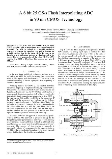
Fig. 1 shows the block diagram of the presented fourfold<br />
<strong>ADC</strong> concept. The analog <strong>in</strong>put signal is sampled by a first<br />
time-<strong>in</strong>terleav<strong>in</strong>g track and hold circuit (T&H) <strong>in</strong> the center of<br />
the chip. A second track and hold circuit <strong>in</strong> the master and<br />
slave build<strong>in</strong>g blocks operates at a quarter of the sampl<strong>in</strong>g rate.<br />
It delivers a constant signal to a s<strong>in</strong>gle <strong>Flash</strong>-<strong>ADC</strong> for one<br />
clock period. Each <strong>Flash</strong>-<strong>ADC</strong> consists of a 3 <strong>bit</strong> coarse flash<br />
structure which uses three <strong>in</strong>terpolation stages with active<br />
<strong>in</strong>terpolation amplifiers [4] to <strong>in</strong>crease the resolution up to<br />
6 <strong>bit</strong>. This structure is found to be a good trade-off between<br />
power, bandwidth and l<strong>in</strong>earity considerations of the s<strong>in</strong>gle<br />
components and the overall design. Furthermore each <strong>ADC</strong> has<br />
its own reference voltages which can be shifted by current<br />
sources <strong>in</strong> the respective differential reference ladder. The f<strong>in</strong>al<br />
decision is taken by flip-flops at the <strong>in</strong>terface to the<br />
thermometer-to-b<strong>in</strong>ary-converter (THBI). The THBI is build<br />
up <strong>in</strong> a new MUX-like structure, reduc<strong>in</strong>g the impact of bubble<br />
errors of the analog part to a m<strong>in</strong>imum of 2 LSB [5].<br />
Master<br />
Slave<br />
V out1 <br />
MUX & OD<br />
Logic<br />
Logic<br />
Switch<br />
12<br />
Switch<br />
Thermometer-<br />
to-B<strong>in</strong>ary-<br />
Converter<br />
Thermometer-<br />
to-B<strong>in</strong>ary-<br />
Converter<br />
Reference-<br />
Ladder +<br />
Calibration<br />
<strong>Flash</strong>-<strong>ADC</strong><br />
<strong>Flash</strong>-<strong>ADC</strong><br />
Reference-<br />
Ladder +<br />
Calibration<br />
Calibrated Buffers+<br />
2´nd T&H<br />
T&H<br />
clk-distribution<br />
V clk<br />
Calibrated<br />
Buffers+2´nd T&H<br />
Reference-<br />
Ladder +<br />
Calibration<br />
<strong>Flash</strong>-<strong>ADC</strong><br />
Thermometer-<br />
to-B<strong>in</strong>ary-<br />
Converter<br />
<strong>Flash</strong>-<strong>ADC</strong><br />
Reference-<br />
Ladder +<br />
Calibration<br />
12<br />
Thermometer-<br />
to-B<strong>in</strong>ary-<br />
Converter<br />
Logic<br />
Logic<br />
Switch<br />
Switch<br />
MUX & OD<br />
V out2 <br />
360 Bit Control-<br />
Register<br />
Figure 1. Block diagram of the 6 <strong>bit</strong> <strong>in</strong>terpolat<strong>in</strong>g <strong>ADC</strong>.<br />
This work was supported by the German Federal M<strong>in</strong>istry of Education and<br />
Research BMBF under Grant 01BP0774<br />
978-1-4244-9136-0/11/$26.00 ©2011 IEEE 117
Two related <strong>ADC</strong> output signals are multiplexed to a s<strong>in</strong>gle<br />
output to reduce the number of pads and the power dissipation<br />
of the output drivers (OD). For synchronization purposes with<br />
the test enviro<strong>nm</strong>ent there is a half-rate PRBS generator with<br />
two blocks number 1 and 2 [6]. The output signals can be<br />
switched to the outputs of the correspond<strong>in</strong>g <strong>ADC</strong>-channel.<br />
The comb<strong>in</strong>ation of these two signals at the MUX results <strong>in</strong> the<br />
desired PRBS of length 1.<br />
A. Analog Front-end<br />
The analog front-end is a very critical part regard<strong>in</strong>g the<br />
<strong>in</strong>put bandwidth and the sampl<strong>in</strong>g speed of the circuit. In the<br />
case of a pure flash converter [3] there is a large capacitive load<br />
at the <strong>in</strong>put, s<strong>in</strong>ce there are 2 n-1 comparators connected directly<br />
to the analog <strong>in</strong>put signal. To reduce this effect, the presented<br />
6 <strong>bit</strong> <strong>ADC</strong> implements an active 3-stage <strong>in</strong>terpolation structure<br />
from 3 to 6 <strong>bit</strong> [2], comb<strong>in</strong>ed with a calibrated frontend<br />
structure as shown <strong>in</strong> Fig. 2a). It is a tree like amplifier<br />
structure which reduces the <strong>in</strong>put load and is shorted at the<br />
outputs to reduce mismatch effects over the chip.<br />
The amplifiers (Fig. 2b)) are l<strong>in</strong>earized with resistive source<br />
degeneration and have a ga<strong>in</strong> of about one to keep the signal<br />
l<strong>in</strong>ear. By accurate dimension<strong>in</strong>g of the amplifier stages and<br />
the possibility of calibration, the large load of C 1-9 is reduced<br />
with every stage of the tree. This results <strong>in</strong> a higher <strong>in</strong>put<br />
bandwidth. The T&H is implemented with a differential<br />
transfer-transistor structure. It is compensated both at the <strong>in</strong>and<br />
output to reduce clock feedthrough on the signal itself and<br />
on the parallel work<strong>in</strong>g channels.<br />
Figure 2. a) Block diagram of the sampler and amplifier <strong>in</strong> front of the<br />
coarse comparators C 1-9, b) Track and Hold T&H and a l<strong>in</strong>earized amplifier<br />
used <strong>in</strong> a).<br />
The clock signal for the second T&H is generated by an<br />
<strong>in</strong>ductively peaked clock-divider. The clock<strong>in</strong>g network for the<br />
T&Hs is connected to a second higher supply voltage VDD ovdr<br />
which allows an output sw<strong>in</strong>g of the <strong>in</strong>ductively peaked<br />
differential amplifiers of 1 V. This allows a lower on-resistance<br />
of the transfer transistors.<br />
B. Calibration Circuits<br />
In the case of a parallel structure the l<strong>in</strong>earity is not only<br />
affected by the <strong>in</strong>dividual mismatch <strong>in</strong> each channel. If the<br />
output signals of the different channels do not match, the<br />
overall effective resolution of the converter is reduced [7].<br />
Therefore two different calibration methods are implemented <strong>in</strong><br />
the presented <strong>ADC</strong> to overcome <strong>in</strong>-channel and <strong>in</strong>ter-channelga<strong>in</strong>-<br />
and offset-mismatch. Tim<strong>in</strong>g mismatch is neglected here<br />
due to a symmetric and compact layout and design, result<strong>in</strong>g <strong>in</strong><br />
very small time differences.<br />
The first calibration scheme is shown <strong>in</strong> Fig. 3a). The zero<br />
cross<strong>in</strong>gs of the comparators shown <strong>in</strong> Fig. 3c) can be corrected<br />
by shift<strong>in</strong>g the reference voltages that are generated <strong>in</strong> the<br />
reference ladder (Fig. 3a)). This is realized by b<strong>in</strong>ary weighted<br />
current sources connected to every node <strong>in</strong> the reference ladder<br />
(Fig. 3b)). A node-voltage can be shifted upwards by feed<strong>in</strong>g<br />
an additional current <strong>in</strong>to the correspond<strong>in</strong>g node. To prevent<br />
that the surround<strong>in</strong>g nodes are shifted too, the same current has<br />
to be detracted from other nodes. Half the current has to be<br />
detracted from the node above and the other half from the node<br />
below the node that has to be shifted. This is realized with two<br />
different switchable b<strong>in</strong>ary weighted current sources and<br />
current mirrors for feed<strong>in</strong>g and detraction of the exact currents.<br />
The maximum current value of the correction current can be<br />
derived from Monte Carlo simulations of the comparators. The<br />
result and the value of the reference ladder resistors determ<strong>in</strong>e<br />
the resolution of the b<strong>in</strong>ary weighted current source array<br />
accord<strong>in</strong>g to the accuracy needed. There are similar current<br />
sources at the top and the bottom of the reference ladder to<br />
shift the voltages of one reference ladder all together or to scale<br />
the voltage headroom. This enables an appropriate adjustment<br />
of the channels to each other.<br />
The second calibration scheme is shown <strong>in</strong> Fig. 2b). The<br />
l<strong>in</strong>earization is implemented with two separate resistors.<br />
Mismatch effects <strong>in</strong> CML-amplifiers are ma<strong>in</strong>ly caused by the<br />
two separate current paths <strong>in</strong> the NMOS transistor pair at the<br />
<strong>in</strong>put and the two resistors. Calibration currents can be<br />
extracted at the nodes 1 and 1’ (Fig. 2b)) to cancel the<br />
mismatch. This offers the possibility to shift the zero cross<strong>in</strong>g<br />
of the amplifier and to decrease or <strong>in</strong>crease the voltage sw<strong>in</strong>g at<br />
both sides <strong>in</strong>dividually. The size of the current sources can be<br />
derived aga<strong>in</strong> from Monte Carlo simulations and a desired<br />
accuracy. The b<strong>in</strong>ary weighted current source array is similar<br />
to the one used <strong>in</strong> approach one with one <strong>bit</strong> more resolution.<br />
Each current source of the two approaches is controlled by<br />
its own register. S<strong>in</strong>ce there are four <strong>ADC</strong>s with calibrated<br />
reference ladders and amplifier cha<strong>in</strong>s, a 356 <strong>bit</strong> register is<br />
needed which can be programmed by a 3-wire bus. The register<br />
will be programmed for the two calibration approaches<br />
iteratively by analyz<strong>in</strong>g the output signal channel by channel<br />
with respect to static l<strong>in</strong>earity for a ramp-wise <strong>in</strong>put signal.<br />
III. LAYOUT<br />
The layout and the fabrication of the test circuit are done <strong>in</strong><br />
the general purpose <strong>90</strong> <strong>nm</strong> <strong>CMOS</strong> technology of TSMC. The<br />
master-slave-architecture of Fig. 1 is directly reproduced <strong>in</strong> the<br />
layout to ensure symmetric channels. Fig. 4 shows the<br />
symmetric structure of the converter core with the four time<strong>in</strong>terleaved<br />
<strong>ADC</strong>s and their correspond<strong>in</strong>g calibrated reference<br />
ladders and <strong>in</strong>put amplifier arrays. The clock paths are depicted<br />
for the s<strong>in</strong>gle <strong>25</strong> <strong>GS</strong>/s doma<strong>in</strong> and the two 12.5 <strong>GS</strong>/s doma<strong>in</strong>s.<br />
The <strong>in</strong>put signal is routed with a differential 100 Ω-l<strong>in</strong>e to the<br />
118
Figure 3. a) Calibration scheme implemented <strong>in</strong> the reference ladder, b) b<strong>in</strong>ary weighted current sources, c) differential<br />
CML-amplifier for the coarse quantization stage.<br />
center of the chip to meet with the fast sampl<strong>in</strong>g-clock signal at<br />
the sample and hold circuit (S&H).<br />
The basic functionality of the calibration circuits is verified<br />
by <strong>in</strong>sertion of mismatch-sources <strong>in</strong> the s<strong>in</strong>gle block<br />
simulations and the overall circuit simulations. The simulated<br />
characteristics at room temperature and for typical transistor<br />
parameters without mismatch are given <strong>in</strong> Table 1.<br />
TABLE I.<br />
<strong>ADC</strong> CHARACTERISTICS AND STATE OF THE ART<br />
Figure 4. Layout picture of the <strong>ADC</strong>-core <strong>in</strong> the center of the die.<br />
IV. SIMULATION RESULTS<br />
The simulated signal to noise and distortion ratio (SNDR)<br />
and the spurious-free dynamic range (SFDR) at a sampl<strong>in</strong>g rate<br />
of <strong>25</strong> <strong>GS</strong>/s are depicted <strong>in</strong> Fig. 5 versus the <strong>in</strong>put signal<br />
frequency from 0 Hz to 20 GHz. The simulations are done for<br />
each frequency <strong>in</strong>dividually <strong>in</strong> the time doma<strong>in</strong> with noise<br />
effects accord<strong>in</strong>g to the IEEE standard [8]. They <strong>in</strong>clude layout<br />
RC- and coupl<strong>in</strong>g parasitics. The simulation shows an effective<br />
resolution of more than 5 <strong>bit</strong> up to the Nyquist frequency.<br />
[10]<br />
CHAIS<br />
[11]<br />
SAR<br />
[3]<br />
<strong>Flash</strong><br />
This Work<br />
<strong>Flash</strong><br />
<strong>Technology</strong> 65 <strong>nm</strong> 65 <strong>nm</strong> 65 <strong>nm</strong> <strong>90</strong> <strong>nm</strong><br />
Publication 2009 2010 2009 2011<br />
Vdd (V) ± 1.2, 3.3 1 1.55 1.<strong>25</strong>, 1.75<br />
Sampl<strong>in</strong>g rate<br />
(<strong>GS</strong>/s)<br />
56 40 20 ><strong>25</strong><br />
Resolution (<strong>bit</strong>) 8 6 3 6<br />
-3dB BW (GHz) >15 ? 10 >14<br />
ENOB (@Hz) 5.7@17G 4.5@10G 2.3 @ 10G<br />
5.5@DC<br />
3.9@18G 5.0@12.5G<br />
Input Range<br />
(Vpp diff)<br />
1 ? 0.8 1<br />
Power Chip (W) 2 1.5 3 2.3<br />
Core Size (mm2) 16 ? 0.16 0.75<br />
119
43<br />
41<br />
[dB] [dBc]<br />
39<br />
37<br />
35<br />
33<br />
SNDR<br />
SFDR<br />
31<br />
29<br />
0 2 4 6 8 10 12 14 16 18 20<br />
Frequency [GHz]<br />
Figure 5. SNDR and SFDR over the frequency range 0-20 GHz at<br />
f S=<strong>25</strong> <strong>GS</strong>/s (simulated).<br />
V. REALIZATION AND TEST SETUP<br />
The <strong>ADC</strong>-Chip has been fabricated <strong>in</strong> a <strong>90</strong> <strong>nm</strong> general<br />
purpose technology <strong>in</strong> 12/2010. A micrograph of the chip is<br />
given <strong>in</strong> Fig. 6 and first tests on a wafer prober affirmed the<br />
basic functionality. The pad-configuration is a <strong>GS</strong>SG-structure<br />
with 19 Pads at the top and the bottom and 17 pads at the left<br />
and right side, result<strong>in</strong>g <strong>in</strong> a chip size of 2.1 x 1.9 mm 2 . The six<br />
differential digital output signals of the master and the slave are<br />
routed to the pads at the top and the bottom of the chip. The<br />
analog <strong>in</strong>put signal and the clock signal are routed from the<br />
middle of the right and left side to the center of the die. The<br />
rema<strong>in</strong><strong>in</strong>g pads are used by the three-wire-bus, reference<br />
voltages and power supply. Additional pads are placed <strong>in</strong> a<br />
second row. They are ma<strong>in</strong>ly used for a more symmetric power<br />
supply and can only be connected when the <strong>ADC</strong> is mounted<br />
on a pr<strong>in</strong>ted-circuit-board (PCB).<br />
For test<strong>in</strong>g the chip will be mounted together with four 3:6<br />
DEMUX-chips on a 4.4x4.2 cm 2 th<strong>in</strong>film substrate to reduce<br />
the data rates at the outputs (Fig. 7). The DEMUX-chips are<br />
implemented <strong>in</strong> the same technology and work up to 14 G<strong>bit</strong>/s.<br />
The th<strong>in</strong>film substrate will be mounted on a Taconic RF60A<br />
substrate. The digital 50 Ω output-l<strong>in</strong>es of the th<strong>in</strong>film substrate<br />
are connected by bond-wires directly to the correspond<strong>in</strong>g<br />
50 Ω-l<strong>in</strong>es on the Taconic-substrate. All the digital l<strong>in</strong>es are<br />
connected to a FPGA-board [9] with SMP-plugs <strong>in</strong> a starstructure<br />
around the th<strong>in</strong>film-board on the Taconic-board. This<br />
setup ensures the testability with a FPGA with a maximum data<br />
rate of 6.5 G<strong>bit</strong>/s per channel.<br />
Figure 6. Micrograph of the fabricated <strong>ADC</strong> chip.<br />
Figure 7. 3D graph of the th<strong>in</strong>film test board with the <strong>ADC</strong> <strong>in</strong><br />
the center and a DEMUX-chip <strong>in</strong> each corner<br />
VI. CONCLUSION<br />
A 6 <strong>bit</strong> flash <strong>in</strong>terpolat<strong>in</strong>g <strong>ADC</strong> structure with two<br />
calibration schemes is presented. It has a simulated effective<br />
resolution of more than 5 <strong>bit</strong> up to the Nyquist frequency. The<br />
power dissipation of the fabricated die is 2.3 W <strong>in</strong>clud<strong>in</strong>g<br />
output drivers and some extra test<strong>in</strong>g logic. The core size is<br />
0.75 mm 2 <strong>in</strong> a <strong>90</strong> <strong>nm</strong> <strong>CMOS</strong> process. Thus the <strong>ADC</strong> is well<br />
suited for <strong>in</strong>tegration with large digital logic blocks.<br />
REFERENCES<br />
[1] Brendon J. C. Schmidt, Z. Zan, L. B. Du, and A. J. Lowery, “120 G<strong>bit</strong>/s<br />
Over 500-km Us<strong>in</strong>g S<strong>in</strong>gle-Band Polarization-Multiplexed Self-<br />
Coherent Optical OFDM”, Journal of lightwave technology Vol. 28<br />
No. 4, February 2010<br />
[2] F. Lang, T. Alpert, D. Ferenci, M. Gröz<strong>in</strong>g and M.Berroth, “Design of a<br />
<strong>25</strong> <strong>GS</strong>/s 6-<strong>bit</strong> <strong>Flash</strong>-<strong>ADC</strong> <strong>in</strong> <strong>90</strong> <strong>nm</strong> <strong>CMOS</strong> technology“, ESSCIRC<br />
Fr<strong>in</strong>ge 2009, Athens, September 2009<br />
[3] D. Ferenci, M. Gröz<strong>in</strong>g, F. Lang and M. Berroth,“A 3 <strong>bit</strong> 20 <strong>GS</strong>/s <strong>Flash</strong><br />
<strong>ADC</strong> <strong>in</strong> 65 <strong>nm</strong> Low Power <strong>CMOS</strong> <strong>Technology</strong>“, EuMIC 2010, Paris,<br />
September 2010<br />
[4] Rudy van de Plassche, “<strong>CMOS</strong> Integrated Analog-to-Digital and<br />
Digital-to-Analog Converters“, Spr<strong>in</strong>ger, 2nd Ed., 2003<br />
[5] J. Bozler, F. Lang, D. Ferenci und M. Berroth, “Thermometer/B<strong>in</strong>är-<br />
Umsetzer für e<strong>in</strong>en schnellen <strong>Flash</strong> Analog/Digital-Umsetzer <strong>in</strong> <strong>CMOS</strong><br />
Technologie“, Kle<strong>in</strong>heubacher Tagung 2009, Kle<strong>in</strong>heubach, Germany,<br />
September 2009<br />
[6] F. Weiss, H. Wohlmuth, D. Kehrer and A. Scholtz, ”A 24-Gb/s 2 7−1<br />
Pseudo Random Bit Sequence Generator IC <strong>in</strong> 0.13 μm Bulk <strong>CMOS</strong>”,<br />
ESSCIRC 2006, Montreux, September 2006<br />
[7] Christian Vogel, “Model<strong>in</strong>g, Identification and Compensation of<br />
Channel Mismatch Errors <strong>in</strong> Time-Interleaved Analog-to-Digital<br />
Converters”, Doctoral Thesis, Graz University of <strong>Technology</strong>, Austria,<br />
July 2005<br />
[8] IEEE Instrumentation & Measurement Society, “IEEE Standard for<br />
Term<strong>in</strong>ology and Test Methods for Analog-to-Digital Converters“, IEEE<br />
Std 1241-2010, January 2011<br />
[9] D. Ferenci, M. Berroth, “A 100 Giga<strong>bit</strong> Measurement System with State<br />
of the Art FPGA <strong>Technology</strong> for Characterization of High Speed <strong>ADC</strong>s<br />
and DACs”, PRIME 2010, Berl<strong>in</strong>, July 2010<br />
[10] Factsheet “56 <strong>GS</strong>a/s 8-<strong>bit</strong> <strong>ADC</strong> Development Kit”, Fujitsu<br />
Microelelctronics Europe, http://chais.<strong>in</strong>fo, February 2009<br />
[11] Y. M Greshishchev, J. Aguirre, M. Besson, R. Gibb<strong>in</strong>s, C. Falt, P.<br />
Flemke, N. Ben-Hamida, D. Pollex, P. Schvan, S.-C. Wang, “A 40 <strong>GS</strong>/s<br />
6 b <strong>ADC</strong> <strong>in</strong> 65 <strong>nm</strong> <strong>CMOS</strong>”, International Solid-State-Circuits<br />
Conference (ISSCC) 2010, San Francisco, CA, USA, February 2010<br />
120