Material properties of Cd1 x Mg x O alloys synthesized by radio ...
Material properties of Cd1 x Mg x O alloys synthesized by radio ...
Material properties of Cd1 x Mg x O alloys synthesized by radio ...

You also want an ePaper? Increase the reach of your titles
YUMPU automatically turns print PDFs into web optimized ePapers that Google loves.
<strong>Material</strong> <strong>properties</strong> <strong>of</strong> <strong>Cd1</strong> x <strong>Mg</strong> x O <strong>alloys</strong> <strong>synthesized</strong> <strong>by</strong> <strong>radio</strong> frequency sputtering<br />
Guibin Chen, K. M. Yu, L. A. Reichertz, and W. Walukiewicz<br />
Citation: Applied Physics Letters 103, 041902 (2013); doi: 10.1063/1.4816326<br />
View online: http://dx.doi.org/10.1063/1.4816326<br />
View Table <strong>of</strong> Contents: http://scitation.aip.org/content/aip/journal/apl/103/4?ver=pdfcov<br />
Published <strong>by</strong> the AIP Publishing<br />
This article is copyrighted as indicated in the abstract. Reuse <strong>of</strong> AIP content is subject to the terms at: http://scitation.aip.org/termsconditions. Downloaded to IP:<br />
166.111.38.22 On: Mon, 04 Nov 2013 08:12:38
APPLIED PHYSICS LETTERS 103, 041902 (2013)<br />
<strong>Material</strong> <strong>properties</strong> <strong>of</strong> Cd 12x <strong>Mg</strong> x O <strong>alloys</strong> <strong>synthesized</strong> <strong>by</strong> <strong>radio</strong> frequency<br />
sputtering<br />
Guibin Chen, 1,2 K. M. Yu, 1,a) L. A. Reichertz, 1,3 and W. Walukiewicz 1<br />
1 <strong>Material</strong>s Sciences Division, Lawrence Berkeley National Laboratory, Berkeley, California 94720, USA<br />
2 Department <strong>of</strong> Physics and Jiangsu Key Laboratory for Chemistry <strong>of</strong> Low Dimensional <strong>Material</strong>s,<br />
Huaiyin Normal University, Jiangsu 223300, People’s Republic <strong>of</strong> China<br />
3 RoseStreet Labs Energy, Phoenix, Arizona 85034, USA<br />
(Received 27 February 2013; accepted 2 July 2013; published online 22 July 2013)<br />
We have studied structural, electrical, and optical <strong>properties</strong> <strong>of</strong> sputter deposited ternary Cd<strong>Mg</strong>O<br />
alloy thin films with total <strong>Mg</strong> concentration as high as 44%. We found that only a fraction<br />
(50%–60%) <strong>of</strong> <strong>Mg</strong> is incorporated as substitutional <strong>Mg</strong> contributing to the modification <strong>of</strong> the<br />
electronic structures <strong>of</strong> the <strong>alloys</strong>. The electrical and optical results <strong>of</strong> the Cd 1 x <strong>Mg</strong> x O<strong>alloys</strong>are<br />
analyzed in terms <strong>of</strong> a large upward shift <strong>of</strong> the conduction band edge with increasing <strong>Mg</strong><br />
concentration. With the increase <strong>of</strong> the intrinsic bandgap, appropriately doped Cd-rich Cd<strong>Mg</strong>O <strong>alloys</strong><br />
can be potentially useful as transparent conductors for photovoltaics. VC 2013 AIP Publishing LLC.<br />
[http://dx.doi.org/10.1063/1.4816326]<br />
Metal oxides have been extensively studied over the last<br />
two decades. 1–6 The reason for the wide interest in these<br />
materials is that they can be highly conductive and transparent<br />
over a wide wavelength region at the same time. Wide gap<br />
oxides such as In 2 O 3 :Sn (ITO) 7–10 or ZnO:Al (AZO) 11–13 are<br />
widely used as transparent contacts on thin film solar cells.<br />
An important limitation in the applications <strong>of</strong> these oxides is<br />
that they have significant long wavelength absorption and<br />
thus cannot be used for photovoltaics that utilize the infrared<br />
part <strong>of</strong> the solar spectrum. The poor infrared transmittance <strong>of</strong><br />
these materials can be attributed to the relatively strong ionized<br />
impurity scattering resulting in low mobility and large<br />
free carrier absorption. In addition, due to the high electron<br />
concentration in these materials (10 21 /cm 3 ) their plasma<br />
reflection edge typically occurs at wavelengths
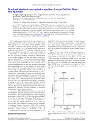
041902-2 Chen et al. Appl. Phys. Lett. 103, 041902 (2013)<br />
FIG. 1. (220) x-ray diffraction peaks from a series <strong>of</strong> Cd 1 x <strong>Mg</strong> x O <strong>alloys</strong><br />
with different substitutional <strong>Mg</strong> concentrations.<br />
substitution <strong>of</strong> Cd with <strong>Mg</strong>. The amount <strong>of</strong> substitutional<br />
<strong>Mg</strong> in Cd 1 x <strong>Mg</strong> x O can be derived from the shift <strong>of</strong> the diffraction<br />
peak using Vegaard’s law. Here we use the values<br />
<strong>of</strong> 4.212 Å and 4.6958 Å for the lattice parameter <strong>of</strong> <strong>Mg</strong>O<br />
and CdO, respectively.<br />
Figure 2(a) compares the <strong>Mg</strong> concentrations determined<br />
<strong>by</strong> XRD with those measured <strong>by</strong> RBS. We note that RBS<br />
measures the total <strong>Mg</strong> concentration whereas peak shifts in<br />
XRD arise from lattice parameter change due to the substitution<br />
<strong>of</strong> Cd with <strong>Mg</strong>. Since the electronic band structure is<br />
affected <strong>by</strong> the composition <strong>of</strong> substitutional <strong>Mg</strong>, therefore,<br />
in the following, the samples will be identified <strong>by</strong> the composition<br />
obtained from the XRD. Figure 2(a) shows that a<br />
significant fraction <strong>of</strong> the total <strong>Mg</strong> is incorporated on nonsubstitutional<br />
sites, most likely in the forms <strong>of</strong> <strong>Mg</strong> interstitials<br />
and <strong>Mg</strong> or <strong>Mg</strong>O precipitates. In Zn<strong>Mg</strong>O <strong>Mg</strong> interstitials<br />
can increase the lattice parameter <strong>of</strong> the alloy and hence partially<br />
compensate the reduction <strong>of</strong> the lattice parameter due<br />
to <strong>Mg</strong> substitution. As a result, if significant amount <strong>of</strong> <strong>Mg</strong><br />
interstitials are present the XRD measurements may underestimate<br />
the substitutional <strong>Mg</strong>. However, we found that as the<br />
FIG. 2. (a) Dependence <strong>of</strong> the substitutional <strong>Mg</strong> concentration on the total<br />
<strong>Mg</strong> concentration. (b) Grain size <strong>of</strong> the Cd 1 x <strong>Mg</strong> x O films as a function <strong>of</strong><br />
<strong>Mg</strong> concentration. The dashed line connecting the data is a polynomial fit to<br />
the data.<br />
FIG. 3. Carrier concentration (n) and mobility (l) as a function <strong>of</strong> <strong>Mg</strong> concentration,<br />
x, in the Cd 1 x <strong>Mg</strong> x O films.<br />
<strong>Mg</strong> composition increases, the electron concentration<br />
decreases in the alloy (Fig. 3), and this does not support the<br />
presence <strong>of</strong> significant amount <strong>of</strong> <strong>Mg</strong> interstitial donors.<br />
This suggests that <strong>Mg</strong> interstitials are not the dominating<br />
defects (
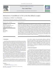
041902-3 Chen et al. Appl. Phys. Lett. 103, 041902 (2013)<br />
FIG. 4. Composition dependence <strong>of</strong> the position <strong>of</strong> the conduction band<br />
edge (solid line) and the Fermi level () <strong>of</strong> the Cd 1 x <strong>Mg</strong> x O samples with<br />
respect to the vacuum level.<br />
FIG. 5. (a) Room-temperature absorption spectra <strong>of</strong> Cd 1 x <strong>Mg</strong> x O films for<br />
various magnesium concentration, x. (b) Dependence <strong>of</strong> the optical gap<br />
E opt<br />
g () and the intrinsic bandgap E g () on <strong>Mg</strong> concentration. The dashed<br />
curve shows the fit to the bandgap energies using a bowing parameter<br />
b ¼ 2.17 eV.<br />
below the vacuum level. This constant level crosses the CBE<br />
and enters the bandgap for x > 0.15. This behavior could be<br />
explained assuming that the electrons in those undoped films<br />
originate from native donor defects with the energy level<br />
located at about 5.4 eV below the vacuum level. As the concentration<br />
<strong>of</strong> electrons depends on the position <strong>of</strong> this level<br />
relative to the CBE it varies from 2 10 20 cm 3 when the<br />
Fermi energy is at E CBE þ 0.5 eV in CdO to low concentrations<br />
when the Fermi energy falls well below CBE for larger<br />
x values. Additionally, at higher compositions the electron<br />
concentration is further reduced due to localization effects<br />
arising from fluctuations <strong>of</strong> the alloy composition. This picture<br />
appears to be consistent with the results <strong>of</strong> the mobility<br />
measurements shown in Fig. 3. The decrease <strong>of</strong> the mobility<br />
at low <strong>Mg</strong> concentration most likely originates from the<br />
alloy disorder scattering although it is possible that it is further<br />
reduced <strong>by</strong> scattering from the grain boundaries since as<br />
it has been shown above the grain size is decreasing with<br />
increasing <strong>Mg</strong> concentration.<br />
The absorption coefficients a <strong>of</strong> films with different <strong>Mg</strong><br />
concentration are shown in Fig. 5(a). A clear blueshift in the<br />
absorption edge is observed with increasing <strong>Mg</strong> concentration.<br />
The absorption edge energy or optical gap, E opt<br />
g ,<strong>of</strong><br />
Cd 1 x <strong>Mg</strong> x O films was obtained <strong>by</strong> linear extrapolations <strong>of</strong><br />
a 2 to the base line in the energy region. The optical gaps,<br />
, as functions <strong>of</strong> x are shown as square symbols in Figure<br />
5(b). However, because <strong>of</strong> large electron concentrations in<br />
some <strong>of</strong> our samples these optical gaps are expected to be<br />
higher than the intrinsic direct gaps E g . Several corrections<br />
have to be taken into account to obtain E g (Ref. 6)<br />
E opt<br />
g<br />
E g ¼ E opt<br />
g DE F Hall ðnÞþDE Ie e ðnÞþDE Ie i ðnÞ; (1)<br />
where the Burstein Moss shift 23,24 DE F-Hall is determined <strong>by</strong><br />
the position <strong>of</strong> the Fermi level in the conduction band and<br />
can be calculated directly from the electron concentration<br />
measured <strong>by</strong> Hall effect, DE Ie-e (n) and DE Ie-i (n) are bandgap<br />
renormalizations due to electron-electron and electron-ion<br />
interactions, respectively. The bandgap renormalizations<br />
were calculated using the formulism in Berggren and<br />
Sernelius 25 and Walukiewicz. 26 The nonparabolic dispersion<br />
relation for the conduction band was derived from Kane’s<br />
two band kp model. 27<br />
The solid triangle symbols in Fig. 5(b) represent the<br />
intrinsic direct gap <strong>of</strong> Cd 1 x <strong>Mg</strong> x O as a function <strong>of</strong> <strong>Mg</strong> concentration<br />
x obtained from Eq. (1), using the conduction<br />
band edge effective mass <strong>of</strong> 0.21m 0 . The bandgap energy<br />
corrections become insignificant, and values <strong>of</strong> E opt<br />
g and E g<br />
are very similar for <strong>alloys</strong> with high <strong>Mg</strong> concentrations<br />
where the electron concentration falls below 10 18 /cm 3 .<br />
Fitting the composition dependence <strong>of</strong> this intrinsic bandgap<br />
to the standard second order formula yields a bandgap bowing<br />
parameter b ¼ 2.17 eV. This bowing parameter is reasonable<br />
comparing to the linear bandgap dependence <strong>of</strong> <strong>Mg</strong> in<br />
Zn<strong>Mg</strong>O <strong>alloys</strong>. 28 Using the same formulism, a much larger<br />
bandgap bowing parameter <strong>of</strong> 5.3 eV is obtained if the RBS<br />
measured <strong>Mg</strong> contents are used.<br />
An ideal transparent conductor on photovoltaic devices<br />
that utilizes most <strong>of</strong> the solar spectrum requires highly conducting<br />
materials (r > 5000 S/cm) with high transparency<br />
from 340 to1300 nm. In our prior work on In and Ga doped<br />
CdO we have achieved thin films with r 15 000 S/cm and<br />
with excellent infrared transparency down to 0.8 eV<br />
(1500 nm) but with too low UV absorption edge at 3.1 eV<br />
(400 nm). 15 Here we show that alloying 10% <strong>of</strong> <strong>Mg</strong>O with<br />
CdO increases the intrinsic bandgap <strong>by</strong> 400 meV, resulting<br />
in a desirable shift <strong>of</strong> the optical absorption edge to higher<br />
energies. However, we note that without any intentional doping,<br />
alloying <strong>of</strong> CdO with <strong>Mg</strong>O results in a reduced electron<br />
mobility and electron concentration resulting in a conductivity<br />
<strong>of</strong>
041902-4 Chen et al. Appl. Phys. Lett. 103, 041902 (2013)<br />
doping <strong>of</strong> Cd-rich Cd 1 x <strong>Mg</strong> x O <strong>alloys</strong> will be required to<br />
determine if similar effects occur in these <strong>alloys</strong> too.<br />
In summary, we have <strong>synthesized</strong> and characterized a<br />
series <strong>of</strong> Cd 1 x <strong>Mg</strong> x O thin films with substitutional <strong>Mg</strong> x up<br />
to 0.28 <strong>by</strong> <strong>radio</strong> frequency magnetron sputtering method. We<br />
found a significant decrease in the grain size with increasing<br />
<strong>Mg</strong> concentration. The reduction <strong>of</strong> the electron concentration<br />
and mobility in these undoped samples is explained <strong>by</strong> a<br />
rapid upward shift <strong>of</strong> the conduction band edge with increasing<br />
<strong>Mg</strong> concentration. Cd-rich Cd<strong>Mg</strong>O <strong>alloys</strong> <strong>of</strong>fer a potential,<br />
as materials, for transparent conductors. We expect that<br />
the electron concentration and mobility <strong>of</strong> Cd 1 x <strong>Mg</strong> x O can<br />
be further increased <strong>by</strong> intentional doping with In or Ga.<br />
Hence, further systematic studies <strong>of</strong> intentional doping and<br />
post-growth annealing will be required to optimize this material<br />
for PV applications.<br />
This material was based upon work supported <strong>by</strong> the<br />
Department <strong>of</strong> Energy through the Bay Area Photovoltaic<br />
Consortium under Award No. DE-EE0004946. G.B.C.<br />
acknowledges the support provided <strong>by</strong> the National Natural<br />
Science Foundation <strong>of</strong> China (No. 11174101), Natural<br />
Science Foundation <strong>of</strong> Jiangsu Province (NSFJS, Nos.<br />
BK2010499, BK2011411, and HAG2011006).<br />
This report was prepared as an account <strong>of</strong> work sponsored<br />
<strong>by</strong> an agency <strong>of</strong> the United States Government. Neither<br />
the United States Government nor any agency there<strong>of</strong>, nor<br />
any <strong>of</strong> their employees, makes any warranty, express or<br />
implied, or assumes any legal liability or responsibility for the<br />
accuracy, completeness, or usefulness <strong>of</strong> any information, apparatus,<br />
product, or process disclosed, or represents that its<br />
use would not infringe privately owned rights. Reference<br />
herein to any specific commercial product, process, or service<br />
<strong>by</strong> trade name, trademark, manufacturer, or otherwise does<br />
not necessarily constitute or imply its endorsement, recommendation,<br />
or favoring <strong>by</strong> the United States Government or<br />
any agency there<strong>of</strong>. The views and opinions <strong>of</strong> authors<br />
expressed herein do not necessarily state or reflect those <strong>of</strong><br />
the United States Government or any agency here<strong>of</strong>.<br />
1 T. Minami, Semicond. Sci. Technol. 20, S35 (2005).<br />
2 Handbook <strong>of</strong> Transparent Conductors, edited <strong>by</strong> D. S. Ginley, H. Hosono,<br />
and D. C. Paine (Springer, New York, 2011).<br />
3 P. D. King and T. D. Veal, J. Phys.: Condens. Matter 23, 334214 (2011).<br />
4 K. L. Chopra, P. D. Paulson, and V. Dutta, Prog. Photovoltaics 12, 69<br />
(2004).<br />
5 S. K. Vasheghani Farahani, T. D. Veal, P. D. C. King, J. Zu~niga-Perez, V.<br />
Mu~noz-Sanjose, and C. F. McConville, J. Appl. Phys. 109, 073712 (2011).<br />
6 A. Segura, J. F. Sanchez-Royo, B. G. Domene, and G. Almonacid, Appl.<br />
Phys. Lett. 99, 151907 (2011).<br />
7 J. C. C. Fan and F. J. Bachner, J. Electrochem. Soc. 122, 1719 (1975).<br />
8 H. Fujiwara and M. Kondo, Phys. Rev. B 71, 075109 (2005).<br />
9 E. Fortunato, D. Gingley, H. Hosono, and D. C. Paine, MRS Bull. 32, 242<br />
(2007).<br />
10 K. Ellmer, Nat. Photonics 6, 809 (2012).<br />
11 C. G. Granqvist, Sol. Energy Mater. Sol. Cells 91, 1529 (2007).<br />
12 K. Fleischer, E. Arca, and I. V. Shvets, Sol. Energy Mater. Sol. Cells 101,<br />
262 (2012).<br />
13 A. Anders, S. H. N. Lim, K. M. Yu, J. Andersson, J. Rosen, M.<br />
McFarland, and J. Brown, Thin Solid Films 518, 3313 (2010).<br />
14 S. Jin, Y. Yang, J. E. Medvedeva, L. Wang, S. Li, N. Cortes, J. R. Ireland,<br />
A. W. Metz, J. Ni, M. C. Hersam, A. J. Freeman, and T. J. Marks, Chem.<br />
Mater. 20, 220 (2008).<br />
15 K. M. Yu, M. A. Mayer, D. T. Speaks, H. He, R. Zhao, L. Hsu, S. S. Mao,<br />
E. E. Haller, and W. Walukiewicz, J. Appl. Phys. 111, 123505 (2012).<br />
16 A. Wang, J. R. Babcock, N. L. Edleman, A. W. Metz, M. A. Lane, R.<br />
Asahi, V. P. Dravid, C. R. Kannewurf, A. J. Freeman, and T. J. Marks,<br />
Proc. Natl. Acad. Sci. U.S.A. 98, 7113 (2001).<br />
17 S. K. Vasheghani Farahani, V. Munoz-Sanjose, J. Zuniga-Perez, C. F.<br />
McConville, and T. D. Veal, Appl. Phys. Lett. 102, 022102 (2013).<br />
18 L. F. J. Piper, A. DeMasi, K. E. Smith, A. Schleife, F. Fuchs, F. Bechstedt,<br />
J. Zuniga-Perez, and V. Munoz-Sanjose, Phys. Rev. B 78, 165127 (2008).<br />
19 D. T. Speaks, M. A. Mayer, K. M. Yu, S. S. Mao, E. E. Haller, and W.<br />
Walukiewicz, J. Appl. Phys. 107, 113706 (2010).<br />
20 P. H. Jefferson, S. A. Hatfield, T. D. Veal, P. D. C. King, C. F.<br />
McConville, J. Zu~niga-Perezb, and V. Mu~noz-Sanjose, Appl. Phys. Lett.<br />
92, 022101 (2008).<br />
21 K. Y. Tsou and E. B. Hensley, J. Appl. Phys. 45, 47 (1974).<br />
22 J. H. Kim, X. Li, L. S. Wang, H. L. de Clercq, C. A. Fancher, O. C.<br />
Thomas, and K. H. Bowen, J. Phys. Chem. A 105, 5709 (2001).<br />
23 E. Burstein, Phys. Rev. 93, 632 (1954).<br />
24 T. S. Moss, Optical Properties <strong>of</strong> Semiconductors (Butterworths, London,<br />
1961).<br />
25 K. F. Berggren and B. E. Sernelius, Phys. Rev. B 24, 1971 (1981).<br />
26 W. Walukiewicz, Phys. Rev. B 41, 10218 (1990).<br />
27 E. O. Kane, J. Phys. Chem. Solids 1, 249 (1957).<br />
28 A. Ohtomo, M. Kawasaki, T. Koida, K. Masubuchi, H. Koinuma, Y.<br />
Sakurai, Y. Yoshida, T. Yasuda, and Y. Segawa, Appl. Phys. Lett. 72,<br />
2466 (1998).<br />
This article is copyrighted as indicated in the abstract. Reuse <strong>of</strong> AIP content is subject to the terms at: http://scitation.aip.org/termsconditions. Downloaded to IP:<br />
166.111.38.22 On: Mon, 04 Nov 2013 08:12:38