Structural, electrical, and optical properties of p-type ZnO thin films ...
Structural, electrical, and optical properties of p-type ZnO thin films ...
Structural, electrical, and optical properties of p-type ZnO thin films ...

You also want an ePaper? Increase the reach of your titles
YUMPU automatically turns print PDFs into web optimized ePapers that Google loves.
<strong>Structural</strong>, <strong>electrical</strong>, <strong>and</strong> <strong>optical</strong> <strong>properties</strong> <strong>of</strong> p-<strong>type</strong> <strong>ZnO</strong> <strong>thin</strong> <strong>films</strong><br />
with Ag dopant<br />
Hong Seong Kang, Byung Du Ahn, Jong Hoon Kim, Gun Hee Kim, Sung Hoon Lim,<br />
Hyun Woo Chang, <strong>and</strong> Sang Yeol Lee a�<br />
Department <strong>of</strong> Electrical <strong>and</strong> Electronic Engineering, Yonsei University, 134 Shinchon-dong,<br />
Seodaemoon-ku, Seoul 120-749, Korea<br />
�Received 11 January 2006; accepted 29 March 2006; published online 17 May 2006�<br />
p-<strong>type</strong> <strong>ZnO</strong> <strong>films</strong> have been fabricated on a �0001� Al2O3 substrate, using Ag2O as a silver dopant<br />
by pulsed laser deposition. The structural property <strong>of</strong> those <strong>films</strong> is systematically characterized by<br />
observing the shift <strong>of</strong> �0002� peak to investigate the substitution <strong>of</strong> Ag + for Zn + . Narrow deposition<br />
temperature for Ag-doped p-<strong>type</strong> <strong>ZnO</strong> <strong>films</strong> has been obtained in the range <strong>of</strong> 200–250 °C with the<br />
hole concentration <strong>of</strong> 4.9�1016 –6.0�1017 cm−3 . A neutral acceptor bound exciton has been clearly<br />
observed by photoluminescence emitted at 3.317 eV in Ag-doped p-<strong>type</strong> <strong>ZnO</strong> <strong>thin</strong> <strong>films</strong>. © 2006<br />
American Institute <strong>of</strong> Physics. �DOI: 10.1063/1.2203952�<br />
<strong>ZnO</strong> is a promising material for the use in ultraviolet or<br />
visible optoelectronic devices, because <strong>of</strong> its direct wide<br />
b<strong>and</strong> gap �3.37 eV� <strong>and</strong> large exciton binding energy<br />
�60 meV�. 1–5 Although it has several advantages compared<br />
to GaN, the difficulty <strong>of</strong> p-<strong>type</strong> doping inhibits applications<br />
to optoelectronic devices. 4,5 It is difficult to fabricate p-<strong>type</strong><br />
<strong>ZnO</strong> because <strong>ZnO</strong> is naturally only n-<strong>type</strong> conduction due to<br />
a large number <strong>of</strong> native defects, such as oxygen vacancies<br />
<strong>and</strong> zinc interstitials. Recently, research on <strong>ZnO</strong> has been<br />
focused on the synthesis <strong>of</strong> p-<strong>type</strong> <strong>ZnO</strong> using various techniques<br />
<strong>and</strong> dopants. 6–17 p-<strong>type</strong> doping in <strong>ZnO</strong> may be possible<br />
by substituting either group I elements �Li, Na, <strong>and</strong> K�<br />
for Zn sites or group V elements �N, P, <strong>and</strong> As� for O sites. 18<br />
Group I elements tend to occupy the interstitial sites rather<br />
than substitutional sites, in part mitigated by their smaller<br />
ionic radii than Zn ionic radius; therefore they act mainly as<br />
donors. 19 Ag, as a group Ib element, could also act as an<br />
acceptor in <strong>ZnO</strong>, if incorporated on substitutional Zn sites. 20<br />
Fan <strong>and</strong> Freer suggested that Ag acted as an amphoteric dopant,<br />
existing both on substitutional Zn sites <strong>and</strong> in the interstitial<br />
sites. 21 Kanai reported that Ag behaves as an acceptor<br />
with a deep level �0.23 eV below the conduction b<strong>and</strong>. 22<br />
However, there is no report for the fabrication <strong>of</strong> p-<strong>type</strong> <strong>ZnO</strong><br />
by doping Ag yet. In this study, p-<strong>type</strong> <strong>ZnO</strong> <strong>films</strong> with Ag<br />
dopant were fabricated by pulsed laser deposition <strong>and</strong> characterized<br />
depending on deposition temperatures. The p-<strong>type</strong><br />
conduction <strong>of</strong> Ag-doped <strong>ZnO</strong> was confirmed by structural,<br />
<strong>electrical</strong>, <strong>and</strong> <strong>optical</strong> characterizations.<br />
Ag, doped <strong>ZnO</strong> �<strong>ZnO</strong>:Ag� <strong>thin</strong> <strong>films</strong> were grown on<br />
�0001� sapphire substrates by pulsed laser deposition �PLD�.<br />
Ag-doped <strong>ZnO</strong> targets were prepared by a conventional ceramic<br />
powder process. A 2 wt. % Ag 2O was mixed with <strong>ZnO</strong><br />
powder for the Ag-doped <strong>ZnO</strong> target. <strong>ZnO</strong>:Ag <strong>thin</strong> <strong>films</strong><br />
were deposited at various temperatures from 100 °C to<br />
400 °C under the oxygen pressure <strong>of</strong> 3.5�10 −1 Torr. The<br />
film thickness was measured to be about 1000 nm confirmed<br />
by scanning electron microscopy �SEM�. The structural<br />
property <strong>of</strong> the samples has been investigated by using x-ray<br />
diffraction �XRD� where a Ni-filtered Cu K� ��<br />
=1.54056 � source was used. The <strong>electrical</strong> property <strong>of</strong> Ag-<br />
a� Electronic mail: sylee@yonsei.ac.kr<br />
APPLIED PHYSICS LETTERS 88, 202108 �2006�<br />
doped <strong>ZnO</strong> <strong>films</strong> has been investigated by Hall measurements<br />
in the van der Pauw configuration at a room temperature.<br />
The <strong>optical</strong> <strong>properties</strong> were characterized by<br />
photoluminescence �PL� with a HeCd laser as a light source<br />
using the excitation wavelength <strong>of</strong> 325 nm <strong>and</strong> the power <strong>of</strong><br />
20 mW.<br />
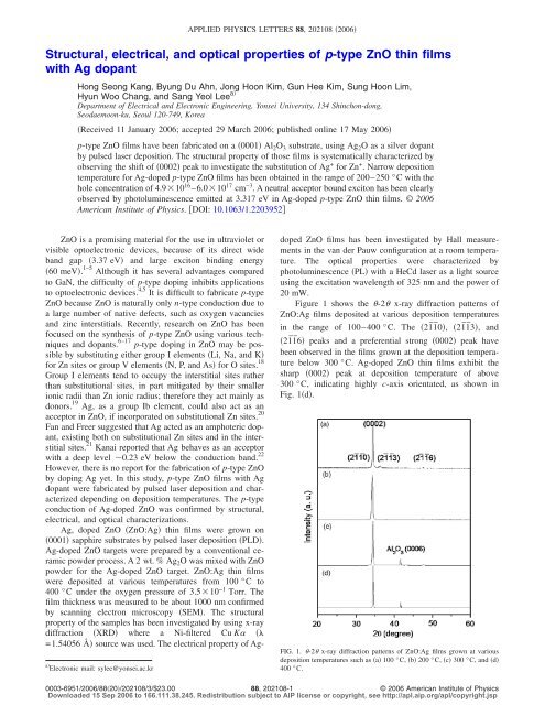
Figure 1 shows the �-2� x-ray diffraction patterns <strong>of</strong><br />
<strong>ZnO</strong>:Ag <strong>films</strong> deposited at various deposition temperatures<br />
in the range <strong>of</strong> 100–400 °C. The �21 ¯1 ¯0�, �21 ¯1 ¯3�, <strong>and</strong><br />
�21 ¯1 ¯6� peaks <strong>and</strong> a preferential strong �0002� peak have<br />
been observed in the <strong>films</strong> grown at the deposition temperature<br />
below 300 °C. Ag-doped <strong>ZnO</strong> <strong>thin</strong> <strong>films</strong> exhibit the<br />
sharp �0002� peak at deposition temperature <strong>of</strong> above<br />
300 °C, indicating highly c-axis orientated, as shown in<br />
Fig. 1�d�.<br />
FIG. 1. �-2� x-ray diffraction patterns <strong>of</strong> <strong>ZnO</strong>:Ag <strong>films</strong> grown at various<br />
deposition temperatures such as �a� 100 °C, �b� 200 °C, �c� 300 °C, <strong>and</strong> �d�<br />
400 °C.<br />
0003-6951/2006/88�20�/202108/3/$23.00 © 2006 American Institute <strong>of</strong> Physics<br />
88, 202108-1<br />
Downloaded 15 Sep 2006 to 166.111.38.245. Redistribution subject to AIP license or copyright, see http://apl.aip.org/apl/copyright.jsp
202108-2 Kang et al. Appl. Phys. Lett. 88, 202108 �2006�<br />
FIG. 2. �a� The change <strong>of</strong> �0002� peak positions <strong>of</strong> <strong>ZnO</strong>:Ag <strong>films</strong>, <strong>and</strong> �b�<br />
that <strong>of</strong> c-axis lattice constant depending on deposition temperature.<br />
The �0002� peak positions <strong>of</strong> Ag-doped <strong>ZnO</strong> <strong>thin</strong> <strong>films</strong><br />
are shifted as changing the deposition temperature, as shown<br />
in Fig. 2�a�. The structural <strong>properties</strong> <strong>of</strong> Ag-doped <strong>ZnO</strong> <strong>films</strong><br />
exhibit three different regions according to their deposition<br />
temperatures, as shown in Fig. 2. Region I is from<br />
100 to 175 °C, region II from 175 to 275 °C, <strong>and</strong> region III<br />
from 275 to 400 °C. The existence <strong>of</strong> three regions is<br />
closely related with the lattice sites <strong>of</strong> Ag in <strong>ZnO</strong>, as reported<br />
by Rita et al. 23 Ag in <strong>ZnO</strong> can act as an amphoteric dopant,<br />
existing both on substitutional Zn sites <strong>and</strong> in the interstitial<br />
sites. 21 The quasichemical reaction for Ag in <strong>ZnO</strong> <strong>thin</strong> <strong>films</strong><br />
may be described as follows:<br />
*<br />
Ag2O → AgZn� +Agi + <strong>ZnO</strong>. �1�<br />
In region I, the Ag + ions cannot substitute Zn2+ ions but<br />
form defects or metallic clusters in the <strong>ZnO</strong> <strong>thin</strong> <strong>films</strong>. This<br />
could be explained mainly because the diffusion behavior <strong>of</strong><br />
Ag in <strong>ZnO</strong> <strong>thin</strong> film is restricted at low temperature <strong>of</strong> below<br />
175 °C. According to Bragg rule, as the peaks <strong>of</strong> �0002�<br />
Ag-doped <strong>ZnO</strong> <strong>films</strong> shift to a lower angle as increasing<br />
deposition temperature in region II, the c-axis lattice constant<br />
increases, as shown in Fig. 2�b�. While as the peaks <strong>of</strong><br />
�0002� Ag-doped <strong>ZnO</strong> shift back to a higher angle as increasing<br />
deposition temperature in region III, the c-axis lattice<br />
constant decreases, as shown in Fig. 2�b�. Because the radius<br />
<strong>of</strong> Ag + ion �1.22 � is a greater than that <strong>of</strong> Zn + ion<br />
�0.72 �, the increase <strong>of</strong> the number <strong>of</strong> Ag + ion in the Zn +<br />
lattice sites exp<strong>and</strong>s the lattice parameter.<br />
Figure 3 shows the carrier concentration �ne or nh� <strong>and</strong><br />
the resistivity ��� <strong>of</strong> Ag-doped <strong>ZnO</strong> <strong>films</strong> at various deposi-<br />
FIG. 3. Carrier concentration <strong>and</strong> resistivity <strong>of</strong> Ag-doped <strong>ZnO</strong> <strong>films</strong> depending<br />
on deposition temperatures ��: hole concentration, �: electron concentration,<br />
<strong>and</strong> �: resistivity�.<br />
tion temperatures. This result is well agreed with three deposition<br />
temperature regions divided by the XRD results, as<br />
shown in Fig. 2. As in the case <strong>of</strong> Ag-doped <strong>ZnO</strong> <strong>films</strong><br />
deposited at region I, it shows semi-insulator behavior, as<br />
shown in Fig. 3�b�. It is noticeable that Ag-doped <strong>ZnO</strong> <strong>films</strong><br />
deposited at region II exhibit p-<strong>type</strong> conductivity. The hole<br />
concentration, hole mobility, <strong>and</strong> resistivity <strong>of</strong> p-<strong>type</strong><br />
Ag-doped <strong>ZnO</strong> <strong>films</strong> are 4.9�1016 –6.0�1017 cm−3 ,<br />
0.29–2.32 cm2 /V s, <strong>and</strong> 34 to 54 � cm, respectively. The<br />
large increase <strong>of</strong> carrier concentration was observed between<br />
regions I <strong>and</strong> II. From the repeated experiments, the existence<br />
<strong>of</strong> critical temperature related to huge increase <strong>of</strong> carrier<br />
concentration has been deserved between 150 <strong>and</strong><br />
200 °C. The Ag-doped <strong>ZnO</strong> <strong>films</strong> deposited at region III<br />
show a conversion <strong>of</strong> n-<strong>type</strong> from p-<strong>type</strong> conductivity with<br />
the electron concentration being increased to 1020 cm−3 .<br />
Other groups also reported same transition behavior related<br />
with group V elements doping. 14,24 These results on the dependence<br />
<strong>of</strong> the conductivity <strong>of</strong> Ag-doped <strong>ZnO</strong> <strong>films</strong> on the<br />
deposition temperature suggest that a narrow temperature<br />
window exists to be p-<strong>type</strong> semiconductor.<br />
Low-temperature �11 K� PL spectra <strong>of</strong> an undoped <strong>ZnO</strong><br />
film <strong>and</strong> p-<strong>type</strong> Ag-doped <strong>ZnO</strong> <strong>thin</strong> film are compared in<br />
Fig. 4. The PL spectra <strong>of</strong> an undoped <strong>ZnO</strong> show various<br />
peaks at 3.359, 3.318, 3.246, <strong>and</strong> 3.174 eV, as shown in Fig.<br />
4�a�. The peaks at 3.359 <strong>and</strong> at 3.318 eV can be assigned to<br />
a neutral donor bound exciton �D 0 X� <strong>and</strong> a donor acceptor<br />
pair �DAP� emission. The peaks at 3.246 <strong>and</strong> 3.174 eV exhibit<br />
phonon replicas <strong>of</strong> DAP separated by approximately<br />
�E=72 meV, which correlates with the longitudinal <strong>optical</strong><br />
phonon energy observed in <strong>ZnO</strong>. 25 The origin <strong>of</strong> emission<br />
line at 3.317 eV <strong>of</strong> Ag doped p-<strong>type</strong> <strong>ZnO</strong>, as shown in Fig.<br />
4�b�, suggested that it was related to neutral acceptor bound<br />
exciton �A 0 X�. The origin <strong>of</strong> emission line at 3.317 eV in<br />
Fig. 4�b� could be explained as two electron satellites �TESs�<br />
or DAP emission compared to other references <strong>and</strong> our result,<br />
as shown in Fig. 4�a�. 20,25,26 However, it is difficult to<br />
observe such a large intensity <strong>of</strong> TES compared to the D 0 X<br />
emission intensity because TES is a kind <strong>of</strong> replica <strong>of</strong> D 0 X<br />
<strong>and</strong> characteristics having specific energy difference �about<br />
29.9 or 55 meV�. 28–30 In the case <strong>of</strong> DAP emission, at low<br />
temperature like 10 K, the intensity <strong>of</strong> DAP emission mainly<br />
shows a low intensity compared with bound exciton<br />
emission, 26,28–30 <strong>and</strong> DAP emission is observed in company<br />
Downloaded 15 Sep 2006 to 166.111.38.245. Redistribution subject to AIP license or copyright, see http://apl.aip.org/apl/copyright.jsp
202108-3 Kang et al. Appl. Phys. Lett. 88, 202108 �2006�<br />
FIG. 4. PL spectra <strong>of</strong> �a� undoped <strong>ZnO</strong>, <strong>and</strong> �b� Ag-doped p-<strong>type</strong> <strong>ZnO</strong> <strong>films</strong><br />
measured at 11 K.<br />
with D 0 X or A 0 X in higher energy region. Therefore, the<br />
origin <strong>of</strong> emission line at 3.317 eV, as shown in Fig. 4�b�,<br />
could be suggested as a neutral bound acceptor exciton <strong>of</strong><br />
Ag-doped p-<strong>type</strong> <strong>ZnO</strong>. This deep acceptor bound exciton<br />
was observed elsewhere. The neutral acceptor bound exciton<br />
emission lines <strong>of</strong> As- <strong>and</strong> N-doped <strong>ZnO</strong> were reported at<br />
3.32 eV measured at 20 K <strong>and</strong> 3.315 eV at 2 K, respectively,<br />
by Ryu et al. 27 <strong>and</strong> Look et al. 28 Also, in the case <strong>of</strong> N-doped<br />
p-<strong>type</strong> <strong>ZnO</strong>, small D 0 X emission <strong>and</strong> large A 0 X emission at<br />
3.315 eV were simultaneously observed at 2 K. These p-<strong>type</strong><br />
<strong>ZnO</strong> <strong>thin</strong> <strong>films</strong> having deep acceptor exciton emission show<br />
the DAP located at about below 3.25 eV. 27,28 These tendencies<br />
are consistent with the results in Fig. 4�b�. The D 0 X<br />
emission at 3.359 eV was observed very weakly because <strong>of</strong><br />
the large <strong>and</strong> broad emission peak <strong>of</strong> A 0 X, as shown in Fig.<br />
4�b�. Peaks at 3.218, 3.147, <strong>and</strong> 2.988 eV were not observed<br />
on PL spectra <strong>of</strong> undoped <strong>ZnO</strong>, as shown in Fig. 4�a�. These<br />
peaks shown in Fig. 4�b� were observed only from Ag-doped<br />
p-<strong>type</strong> <strong>ZnO</strong> <strong>and</strong> suggest that they are closely related to Agrelated<br />
impurity or defect level transition. However, further<br />
investigation is necessary to verify exact origin <strong>of</strong> these<br />
peaks.<br />
In summary, Ag-doped p-<strong>type</strong> <strong>ZnO</strong> <strong>thin</strong> <strong>films</strong> have been<br />
fabricated <strong>and</strong> characterized. A systematic investigation on<br />
the effect <strong>of</strong> deposition temperature has been carried out for<br />
Ag-doped <strong>ZnO</strong> <strong>films</strong>. A narrow window <strong>of</strong> deposition temperature<br />
existed for <strong>films</strong> doped with Ag, in which p-<strong>type</strong><br />
<strong>ZnO</strong> <strong>films</strong> could be obtained. The fabricated Ag-doped<br />
p-<strong>type</strong> <strong>ZnO</strong> film shows the hole concentration in the<br />
range <strong>of</strong> 4.9�10 16 –6.0�10 17 cm −3 , the hole mobility <strong>of</strong><br />
0.29–2.32 cm 2 /V s, <strong>and</strong> the resistivity <strong>of</strong> 34–54 � cm. A<br />
neutral acceptor bound exciton peak <strong>of</strong> 3.317 eV was also<br />
observed in Ag-doped <strong>ZnO</strong>.<br />
This work was supported by Grant No. R01-2004-000-<br />
10195-0 �2005� from the Basic Research Program <strong>of</strong> the<br />
Korea Science <strong>and</strong> Engineering Foundation.<br />
1 D. C. Look, Semicond. Sci. Technol. 20, S55�2005�.<br />
2 D. C. Look, Mater. Sci. Eng., B 80, 383 �2001�.<br />
3 H. Ohota, K. Kawamura, M. Orita, M. Hirano, N. Sarukura, <strong>and</strong> H.<br />
Hosono, Appl. Phys. Lett. 77, 475 �2000�.<br />
4 S. Y. Lee, Y. Li, J. S. Lee, J. K. Lee, M. Nastasi, S. A. Crooker, Q. X. Jia,<br />
H. S. Kang, <strong>and</strong> J. S. Kang, Appl. Phys. Lett. 85, 218 �2003�.<br />
5 H. S. Kang, J. S. Kang, J. W. Kim, <strong>and</strong> S. Y. Lee, J. Appl. Phys. 95, 1246<br />
�2004�.<br />
6 K.-K. Kim, H.-S. Kim, D.-K. Kwang, J.-H. Lim, <strong>and</strong> S.-J. Park, Appl.<br />
Phys. Lett. 83, 63�2003�.<br />
7 C. C. Lin, S. Y. Chen, S. Y. Cheng, <strong>and</strong> H. Y. Lee, Appl. Phys. Lett. 84,<br />
5040 �2004�.<br />
8 Y. R. Ryu, T. S. Lee, <strong>and</strong> H. W. White, Appl. Phys. Lett. 83, 87�2003�.<br />
9 S. Y. Lee, E. S. Shim, H. S. Kang, S. S. Pang, <strong>and</strong> J. S. Kang, Thin Solid<br />
Films 473, 31�2005�.<br />
10 A. Kobayashi, O. F. Sankey, <strong>and</strong> J. D. Dow, Phys. Rev. B 28, 946�1983�.<br />
11 T. Aoki, Y. Hatanaka, <strong>and</strong> D. C. Look, Appl. Phys. Lett. 76, 3257 �2000�.<br />
12 D. C. Look, G. M. Renlund, R. H. Burgener II, <strong>and</strong> J. R. Sizelove, Appl.<br />
Phys. Lett. 85, 5269 �2004�.<br />
13 F. X. Xiu, Z. Yang, L. J. M<strong>and</strong>alapu, D. T. Zhao, <strong>and</strong> J. L. Liu, Appl. Phys.<br />
Lett. 87, 152101 �2005�.<br />
14 V. Vaithianathan, B.-T. Lee, <strong>and</strong> S. S. Kim, J. Appl. Phys. 98, 043519<br />
�2005�.<br />
15 J. G. Lu, Z. Z. Ye, F. Zhuge, Y. J. Zeng, B. H. Zhao, <strong>and</strong> L. P. Zhu, Appl.<br />
Phys. Lett. 85, 3134 �2004�.<br />
16 M. Joseph, H. Tabata, H. Saeki, K. Ueda, <strong>and</strong> T. Kawai, Physica B 302,<br />
140 �2001�.<br />
17 A. V. Singh, R. M. Mehra, A. Wakahara, <strong>and</strong> A. Yoshida, J. Appl. Phys.<br />
93, 396 �2003�.<br />
18 C. H. Park, S. B. Zhang, <strong>and</strong> Su-Huai Wei, Phys. Rev. B 66, 073202<br />
�2002�.<br />
19 D. C. Look, R. L. Jones, J. R. Sizelove, N. Y. Garces, N. C. Giles, <strong>and</strong> L.<br />
E. Halliburton, Phys. Status Solidi A 195, 171 �2003�.<br />
20 C. F. Klingshirn, Semiconductor Optics �Springer, Berlin, 1995�.<br />
21 J. Fan <strong>and</strong> R. Freer, J. Appl. Phys. 77, 9�1995�.<br />
22 Y. Kanai, Jpn. J. Appl. Phys., Part 1 30, 2021 �1991�.<br />
23 E. Rita, U. Wahl, A. M. L. Lopes, J. P. Araújo, J. G. Correia, E. Alves, J.<br />
C. Soares, <strong>and</strong> The ISOLDE Collaboration, Physica B 340, 240�2003�.<br />
24 G. D. Yuan, Z. Z. Ye, L. P. Zhu, Q. Qian, B. H. Zhao, <strong>and</strong> R. X. Fan, Appl.<br />
Phys. Lett. 86, 202106 �2005�.<br />
25 S. A. Studenikin, Michael Cocivera, W. Kellner, <strong>and</strong> H. Pascher, J. Lumin.<br />
91, 223 �2000�.<br />
26 Ü. Özgür, Ya. I. Alivov, C. Liu, A. Teke, M. A. Reshchikov, S. Doğan, V.<br />
Avrutin, S.-J. Cho, <strong>and</strong> H. Morkoç, J. Appl. Phys. 98, 041301 �2005�.<br />
27 Y. R. Ryu, S. Zhu, D. C. Look, J. M. Wrobel, H. M. Jeong <strong>and</strong> H. W.<br />
White, J. Cryst. Growth 216, 330 �2000�.<br />
28 D. C. Look, D. C. Reynolds, C. W. Litton, R. L. Jones, D. B. Eason, <strong>and</strong><br />
G. Cantwell, Appl. Phys. Lett. 81, 1830 �2002�.<br />
29 D. C. Reynolds, D. C. Look, B. Jogai, C. W. Litton, T. C. Collins, W.<br />
Harsch, <strong>and</strong> G. Cantwell, Phys. Rev. B 57, 12151 �1998�.<br />
30 K. Thonke, Th. Gruber, N. Te<strong>of</strong>ilov, R. Schönfelder, A. Waag, <strong>and</strong> R.<br />
Sauer, Physica B 308–310, 945 �2001�.<br />
Downloaded 15 Sep 2006 to 166.111.38.245. Redistribution subject to AIP license or copyright, see http://apl.aip.org/apl/copyright.jsp