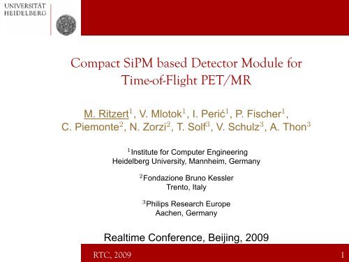
Compact SiPM based Detector Module for Time-of-Flight PET/MR
Compact SiPM based Detector Module for Time-of-Flight PET/MR
Compact SiPM based Detector Module for Time-of-Flight PET/MR

Create successful ePaper yourself
Turn your PDF publications into a flip-book with our unique Google optimized e-Paper software.
<strong>Compact</strong> <strong>SiPM</strong> <strong>based</strong> <strong>Detector</strong> <strong>Module</strong> <strong>for</strong><br />
<strong>Time</strong>-<strong>of</strong>-<strong>Flight</strong> <strong>PET</strong>/<strong>MR</strong><br />
M. Ritzert 1 , V. Mlotok 1 , I. Perić 1 , P. Fischer 1 ,<br />
C. Piemonte 2 , N. Zorzi 2 , T. Solf 3 , V. Schulz 3 , A. Thon 3<br />
1 Institute <strong>for</strong> Computer Engineering<br />
Heidelberg University, Mannheim, Germany<br />
2 Fondazione Bruno Kessler<br />
Trento, Italy<br />
3 Philips Research Europe<br />
Aachen, Germany<br />
Realtime Conference, Beijing, 2009<br />
RTC, 2009 1
Project Overview<br />
I Project funded by the European Union in FP7.<br />
I Develop a compact <strong>PET</strong> detector module <strong>for</strong> use in a<br />
simultaneous ToF <strong>PET</strong>/<strong>MR</strong> detector, scalable to a<br />
whole-body scanner.<br />
I Develop novel reconstruction algorithms to make<br />
good use <strong>of</strong> the available in<strong>for</strong>mation (<strong>MR</strong> <strong>based</strong><br />
attenuation and motion correction).<br />
RTC, 2009 2
Requirements <strong>for</strong> the <strong>PET</strong> <strong>Detector</strong><br />
I <strong>MR</strong> compatible design, i.e. no magnetic components,<br />
especially no PMTs, inside the magnet, no wire loops.<br />
I Fit inside the little available space inside the <strong>MR</strong><br />
scanner.<br />
1. Develop a compact detector module.<br />
2. Require few wire and other connections through the<br />
<strong>MR</strong> scanner.<br />
I No relevant per<strong>for</strong>mance degredation by <strong>MR</strong><br />
gradients and HF signals from <strong>MR</strong> operation.<br />
I Sub-nanosecond timing <strong>for</strong> ToF <strong>PET</strong>.<br />
I Several thousand channels even in a “small” animal<br />
scanner.<br />
I Rugged design to withstand the vibrations inside an<br />
<strong>MR</strong> scanner.<br />
RTC, 2009 3
State <strong>of</strong> the Art in Simultaneous <strong>PET</strong>/<strong>MR</strong><br />
I Use a light guide to guide the scintillation light to PMT<br />
detectors outside the magnet.<br />
Drawback: Lots <strong>of</strong> optical fibres, bad light yield.<br />
I APD detectors with first<br />
amplification stage inside<br />
the field, all other<br />
processing outside the B<br />
field.<br />
Drawback: Lots <strong>of</strong><br />
connections required,<br />
potential <strong>of</strong> large noise<br />
pickup on long wires.<br />
→ Not scalable.<br />
M. Judenh<strong>of</strong>er et al., “Simultaneous <strong>PET</strong>-<strong>MR</strong>I:<br />
a new approach <strong>for</strong> functional and morphological<br />
imaging,” Nature Medicine 14, 459 - 465<br />
(2008)<br />
RTC, 2009 4
Our Approach<br />
Put everything inside the tube:<br />
I Light detection<br />
I Amplification<br />
I Digitization<br />
I <strong>Time</strong>stamping<br />
I Serialization<br />
→ Only few data connections <strong>for</strong> a large number <strong>of</strong><br />
channels.<br />
RTC, 2009 5
Methods<br />
I Highly integrated<br />
electronics.<br />
I Very compact module<br />
design.<br />
I Large area <strong>SiPM</strong><br />
detectors.<br />
I Aggressive mechanics<br />
and cooling.<br />
I Differential architecture<br />
<strong>for</strong> EMI robustness. Actual size: 33×33 mm².<br />
I Modular concept with<br />
defined interfaces on the<br />
connectors.<br />
RTC, 2009 6
Block Diagram<br />
Power<br />
3 rd PCB 2 nd PCB 1 st PCB<br />
LDO<br />
to DAQ<br />
FPGA<br />
Readout<br />
Readout<br />
ASIC<br />
ASIC<br />
Impedance<br />
Matching<br />
DACs<br />
digital<br />
analog<br />
to HV<br />
suply<br />
RTC, 2009 7
Top PCB: <strong>Detector</strong>s<br />
I 64 channels.<br />
I 4×4 mm² <strong>SiPM</strong>s.<br />
I 4×4 monolithic arrays <strong>of</strong> 2×2 silicon<br />
photomultipliers.<br />
→ Entire surface covered by <strong>SiPM</strong>s<br />
→ High packing fraction.<br />
I Passive components required to<br />
interface to the ASICs located on<br />
the bottom side <strong>of</strong> the PCB.<br />
RTC, 2009 8
Middle PCB: Hit Digitizing<br />
I Two readout ASICs, each handling<br />
32 <strong>SiPM</strong> channels.<br />
I Self-triggering by leading-edge<br />
discriminator.<br />
I 100 ps FWHM coincidence timing<br />
resolution.<br />
I 20 bit timestamps.<br />
I 9 bit ADC <strong>for</strong> energy readout.<br />
I Digitization <strong>of</strong> absolute arrival time<br />
and signal energy.<br />
I All-digitial, differential output to the<br />
FPGA.<br />
RTC, 2009 9
Bottom PCB: Control, Processing<br />
I Xilinx Spartan FPGA <strong>for</strong><br />
I Control <strong>of</strong> the ASICs.<br />
I Hit data preprocessing.<br />
I Interfacing between the ASICs and<br />
the system.<br />
I DACs to generate bias voltages <strong>for</strong><br />
the ASICs and <strong>SiPM</strong> devices.<br />
I Interface to DAQ: Several LVDS<br />
connections.<br />
I Local analog power regulation.<br />
RTC, 2009 10
Test Setup<br />
I Testboard<br />
containing a single<br />
PCB stack and<br />
interface to USB.<br />
I Light-tight box <strong>for</strong><br />
measurements<br />
with <strong>SiPM</strong>s.<br />
I <strong>Detector</strong> board replaced with dummy board<br />
connecting pulse inputs to SMA connectors <strong>for</strong> ASIC<br />
characterization.<br />
I Linux-<strong>based</strong> data acquisition and data analysis.<br />
RTC, 2009 11
Results – Setup Verification<br />
Counts<br />
25 k<br />
20 k<br />
15 k<br />
10 k<br />
5 k<br />
Measurement<br />
19.7% FWHM<br />
0<br />
0 400 800 1200<br />
Energy [keV]<br />
22 Na spectrum measured with a single LYSO crystal<br />
standing on one <strong>SiPM</strong>. Bad optical coupling! → Bad<br />
resolution.<br />
But: Proves that the entire stack works as expected!<br />
RTC, 2009 12
Results – Discriminator Threshold<br />
100<br />
Triggers Seen [%]<br />
80<br />
60<br />
40<br />
20<br />
0<br />
Measurement<br />
3.0 m ± 626 µV<br />
2 2.5 3 3.5 4 4.5<br />
Trigger Voltage [mV]<br />
RTC, 2009 13
Results – Threshold Dispersion I<br />
Discriminator Schematics<br />
Threshold<br />
Setting<br />
differential<br />
pair input<br />
Pulse Input<br />
Expected Behavior<br />
Disabled<br />
several σ noise<br />
Trigger<br />
Out<br />
Trigger Rate<br />
0<br />
bar range<br />
in next plot<br />
Threshold Setting<br />
RTC, 2009 14
Results – Threshold Dispersion II<br />
60 m<br />
Threshold Setting [V]<br />
40 m<br />
20 m<br />
0<br />
-20 m<br />
-40 m<br />
0 10 20 30 40 50 60 70<br />
Channel<br />
RTC, 2009 15
Results – Threshold Dispersion III<br />
I Bar <strong>of</strong>fset: Switching <strong>of</strong>fset <strong>of</strong> a differential pair <strong>of</strong><br />
NMOS transistors in close proximity.<br />
I Effects: Large threshold dispersion between<br />
channels, limit on lowest possible threshold.<br />
I Compensation circuit implemented in next generation<br />
ASIC.<br />
RTC, 2009 16
Future System Integration<br />
I Motherboard PCB with<br />
six (3×2) stacks with<br />
minimal spacing.<br />
I Large FPGA to process<br />
the data and send it <strong>of</strong>f<br />
via Gigabit Ethernet.<br />
I Box to firmly hold the<br />
components and provide<br />
the infrastructure <strong>for</strong><br />
cooling.<br />
RTC, 2009 17
Outlook<br />
I Improved ASIC<br />
I Decreased discriminator threshold dispersion.<br />
I Lower power consumption.<br />
I Should be back from fabrication just today.<br />
I Operation with full crystal array.<br />
I Measure per<strong>for</strong>mance in <strong>MR</strong>.<br />
RTC, 2009 18
Acknowledgements<br />
This project is supported by the European Union under the<br />
7 th framework program (Grant Agreement #201651).<br />
RTC, 2009 19