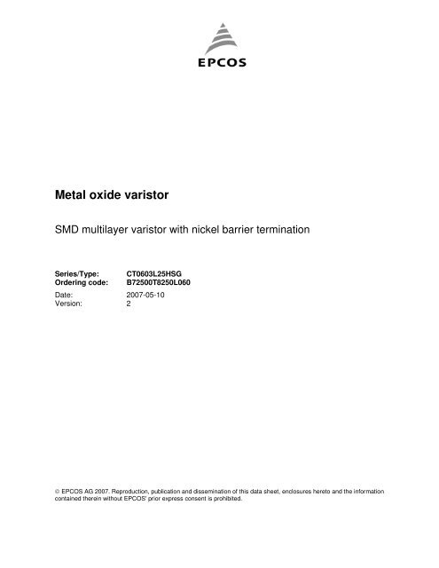
Metal oxide varistors, CT0603L25HSG
Metal oxide varistors, CT0603L25HSG
Metal oxide varistors, CT0603L25HSG

Create successful ePaper yourself
Turn your PDF publications into a flip-book with our unique Google optimized e-Paper software.
<strong>Metal</strong> <strong>oxide</strong> varistor<br />
SMD multilayer varistor with nickel barrier termination<br />
Series/Type:<br />
Ordering code:<br />
<strong>CT0603L25HSG</strong><br />
B72500T8250L060<br />
Date: 2007-05-10<br />
Version: 2<br />
Content of header bars 1 and 2 of data sheet will be automatically entered in headers and footers! Please fill in the<br />
table and then change the color to "white" (or invisible). This ensures that the table disappears for the customer<br />
PDF. To update the data sheet, click on the symbol "Preview" and then "Close". Please do not alter the header or<br />
footer when copying the content.<br />
Identification/Classification 1: (header 1 + top left header bar)<br />
Identification/Classification 2: (header 2 + bottom left header bar)<br />
Ordering code: (top right header bar)<br />
Series/Type: (top right header bar)<br />
Preliminary data (optional): (if necessary)<br />
Department:<br />
<strong>Metal</strong> <strong>oxide</strong> varistor<br />
SMD multilayer varistor with nickel barrier termination<br />
B72500T8250L060<br />
<strong>CT0603L25HSG</strong><br />
KB VS PE<br />
Date: 2007-05-10<br />
Prepared by :<br />
Release signed PE:<br />
Release signed QS:<br />
Modifications / Remarks:<br />
Dr. Krenn<br />
Dr. Engel<br />
Hr. Schlauer<br />
Actualization of data sheet format for internet.<br />
© EPCOS AG 2007. Reproduction, publication and dissemination of this data sheet, enclosures hereto and the information<br />
contained therein without EPCOS' prior express consent is prohibited.
<strong>Metal</strong> <strong>oxide</strong> varistor<br />
SMD multilayer varistor with nickel barrier termination<br />
B72500T8250L060<br />
<strong>CT0603L25HSG</strong><br />
Designation system<br />
CT = chip with three-layer-termination (Ag/Ni/Sn)<br />
0603 = dimensions of the device 06 x 03 (length x width in 1/100 inch)<br />
L = tolerance of the varistor voltage (±15%)<br />
25 = maximum operating voltage (RMS voltage)<br />
HS = designed for protection of high speed data lines<br />
G = taped version (cardboard tape, 7” reel, 4000 pcs. /reel)<br />
Electrical data<br />
Maximum operating voltage<br />
RMS voltage<br />
DC voltage<br />
V RMS = 25 V<br />
V DC = 32 V<br />
Varistor voltage (@ 1 mA, 25 °C)<br />
V V = 51.9 … 70.1 V<br />
Maximum clamping voltage (@ 1 A)<br />
V C = 120 V<br />
Maximum surge current (8/20 µs)<br />
I max = 1 x 5 A<br />
Maximum energy absorption (ESD)<br />
E max = 50 mJ<br />
(@ ESD to ISO TR10605, 25 kV air discharge, 150 pF, 2 kΩ)<br />
Capacitance (@ 1 MHz, 1V, 25 °C, typ.)<br />
Capacitance (@ 1 MHz, 1V, 25 °C)<br />
C = 10 pF<br />
C max = 15 pF<br />
Response time<br />
< 0.5 ns<br />
Operating temperature –55 … +125 °C<br />
Storage temperature (mounted parts) –55 … +150 °C<br />
Complies with following ESD standards<br />
IEC 61000-4-2 level 4 (8 kV contact, 15 kV air discharge)<br />
ISO TR10605 level 4 (25 kV air discharge)<br />
AEC Q200 002 level 6 (25 kV air discharge)<br />
KB VS PE 2007-05-10<br />
Please read Important notes at the end Page 2 of 10<br />
of this document.
<strong>Metal</strong> <strong>oxide</strong> varistor<br />
SMD multilayer varistor with nickel barrier termination<br />
B72500T8250L060<br />
<strong>CT0603L25HSG</strong><br />
v/i characteristic<br />
v<br />
400<br />
V<br />
200<br />
VAR9737A<br />
100<br />
80<br />
60<br />
40<br />
20<br />
10<br />
8<br />
6<br />
4<br />
2<br />
1<br />
10 -5 10 -4 10 -3 10 -2 10 -1 10 0 A 10 1<br />
i<br />
Temperature derating<br />
Max. current, energy, operating voltage and average power<br />
dissipation depending on ambient temperature<br />
%<br />
100<br />
90<br />
80<br />
70<br />
60<br />
50<br />
40<br />
30<br />
20<br />
10<br />
0<br />
-55 70 80 90 100 110 120 130 140 150 °C<br />
Ambient temperature<br />
KB VS PE 2007-05-10<br />
Please read Important notes at the end Page 3 of 10<br />
of this document.
<strong>Metal</strong> <strong>oxide</strong> varistor<br />
SMD multilayer varistor with nickel barrier termination<br />
B72500T8250L060<br />
<strong>CT0603L25HSG</strong><br />
Stability to multiple ESD pulses 1)<br />
80<br />
60<br />
40<br />
20<br />
0<br />
0 1 10 100 1000 10000<br />
number of ESD pulses<br />
1) 15 kV air discharge, 150 pF, 330 Ω, according to IEC 61000-4-2<br />
Signal insertion loss 2)<br />
0.00<br />
-0.50<br />
insertion loss [dB]<br />
-1.00<br />
-1.50<br />
-2.00<br />
-2.50<br />
-3.00<br />
0 20 40 60 80 100<br />
frequency [MHz]<br />
2) typical values, measured with network analyzer HP8753 E/S containing S-parameter test set.<br />
KB VS PE 2007-05-10<br />
Please read Important notes at the end Page 4 of 10<br />
of this document.
<strong>Metal</strong> <strong>oxide</strong> varistor<br />
SMD multilayer varistor with nickel barrier termination<br />
B72500T8250L060<br />
<strong>CT0603L25HSG</strong><br />
Dimensional drawing in mm<br />
l = 1.6 ±0.15<br />
b = 0.8 ±0.1<br />
s = 0.9 max<br />
k = 0.1 … 0.4<br />
Recommended solder pad layout<br />
B<br />
C<br />
B<br />
A<br />
D<br />
A<br />
A = 1.0 mm<br />
B = 1.0 mm<br />
C = 1.0 mm<br />
D = 3.0 mm<br />
KB VS PE 2007-05-10<br />
Please read Important notes at the end Page 5 of 10<br />
of this document.
<strong>Metal</strong> <strong>oxide</strong> varistor<br />
SMD multilayer varistor with nickel barrier termination<br />
B72500T8250L060<br />
<strong>CT0603L25HSG</strong><br />
Recommended soldering temperature profiles<br />
Reflow soldering temperature profile<br />
t p<br />
T p<br />
Temperature<br />
T L<br />
TSmax<br />
Ramp-up<br />
t L<br />
Critical zone<br />
TL<br />
to T p<br />
TSmin<br />
t S Preheat<br />
Ramp-down<br />
25<br />
t 25 ˚C to peak<br />
Time<br />
TPT0892-3-E<br />
Profile feature Sn-Pb eutectic assembly Pb-free assembly<br />
Average ramp-up rate (T Smax to T p ) 3 °C/ second max. 3 °C/ second max.<br />
Preheat<br />
- Temperature min (T Smin )<br />
- Temperature max (T Smax )<br />
- Time (t Smin to t Smax )<br />
Time maintained above<br />
- Temperature min (T L )<br />
- Time (t L )<br />
100 °C<br />
150 °C<br />
60 … 120 seconds<br />
150 °C<br />
200 °C<br />
60 … 180 seconds<br />
183 °C<br />
217 °C<br />
60 … 150 seconds<br />
60 … 150 seconds<br />
220 °C … 240 °C 240 °C … 260 °C<br />
Peak classification temperature<br />
(T p )<br />
Time within 5 °C of actual peak 10 … 30 seconds 20 … 40 seconds<br />
temperature (t p )<br />
Ramp-down rate 6 °C/ second max. 6 °C/ second max.<br />
Time 25 °C to peak temperature 6 minutes max. 8 minutes max.<br />
Notes: All temperatures refer to topside of the package, measured on the package body surface.<br />
Max. number of reflow cycles: 3<br />
KB VS PE 2007-05-10<br />
Please read Important notes at the end Page 6 of 10<br />
of this document.
<strong>Metal</strong> <strong>oxide</strong> varistor<br />
SMD multilayer varistor with nickel barrier termination<br />
B72500T8250L060<br />
<strong>CT0603L25HSG</strong><br />
Wave soldering temperature profile<br />
Temperature characteristic at component terminal with dual-wave soldering<br />
300<br />
˚C<br />
10 s<br />
Normal curve<br />
Limit curves<br />
250<br />
235 ˚C ... 260 ˚C<br />
Temperature<br />
200<br />
150<br />
1st wave<br />
approx. 200 K/s<br />
2nd wave<br />
5 K/s<br />
2 K/s<br />
100<br />
100 ˚C ... 130 ˚C<br />
50<br />
2 K/s<br />
Forced<br />
cooling<br />
0<br />
0<br />
50<br />
100<br />
150<br />
200<br />
Time<br />
s 250<br />
KKE0144-J-E<br />
Soldering guidelines<br />
The usage of mild, non-activated fluxes for soldering is recommended, as well as proper cleaning of<br />
the PCB.<br />
The components are suitable for reflow soldering to JEDEC J-STD-020C.<br />
Storage condition<br />
As far as possible, the components should be employed within 12 months after delivery from<br />
EPCOS.<br />
They should be left in their original packings to avoid soldering problems due to oxidized<br />
contacts.<br />
Storage temperature: − 25 up to + 45°C.<br />
Relative humidity: < 75 % annual average, < 95 % on max. 30 days in a year.<br />
KB VS PE 2007-05-10<br />
Please read Important notes at the end Page 7 of 10<br />
of this document.
<strong>Metal</strong> <strong>oxide</strong> varistor<br />
SMD multilayer varistor with nickel barrier termination<br />
B72500T8250L060<br />
<strong>CT0603L25HSG</strong><br />
Taping and packaging<br />
Tape and reel packing according to IEC 60286-3<br />
Tape material: Cardboard<br />
T<br />
D<br />
P<br />
0 2<br />
P<br />
0<br />
T<br />
1<br />
T 2<br />
T 1<br />
A<br />
0<br />
B 0<br />
P 1<br />
G F E<br />
W<br />
Direction of unreeling<br />
Dimensions and tolerances<br />
Definition Symbol Dimension<br />
[mm]<br />
Tolerance<br />
[mm]<br />
Compartment width A 0 0.95 ±0.2<br />
Compartment length B 0 1.8 ±0.2<br />
Sprocket hole diameter D 0 1.5 +0.1 /-0<br />
Sprocket hole pitch P 0 4.0 ±0.1 1)<br />
Distance center hole to center compartment P 2 2.0 ±0.05<br />
Pitch of the component compartments P 1 4.0 ±0.1<br />
Tape width W 8.0 ±0.3<br />
Distance edge to center of hole E 1.75 ±0.1<br />
Distance center hole to center compartment F 3.5 ±0.05<br />
Distance compartment to edge G 0.75 min.<br />
Overall thickness T 2 1.1 max.<br />
Thickness tape T 0.9 max.<br />
1) ≤ ± 0.2 mm over any 10 pitches<br />
Package: 8-mm tape<br />
KB VS PE 2007-05-10<br />
Please read Important notes at the end Page 8 of 10<br />
of this document.
<strong>Metal</strong> <strong>oxide</strong> varistor<br />
SMD multilayer varistor with nickel barrier termination<br />
B72500T8250L060<br />
<strong>CT0603L25HSG</strong><br />
Packing<br />
Packing material: Plastic<br />
Reel dimensions<br />
Tape end (trailer)<br />
Leader<br />
40 min.<br />
empty cavities<br />
25 min.<br />
empty cavities<br />
300 mm<br />
cover tape<br />
Definition Symbol Dimension<br />
[mm]<br />
Tolerance<br />
[mm]<br />
Reel diameter A 180 +0 / -3<br />
Reel width (inside) W 1 8.4 +1.5 / -0<br />
Reel width (outside) W 2 14.4 max.<br />
Packing unit: 4000 pcs. / reel<br />
.<br />
KB VS PE 2007-05-10<br />
Please read Important notes at the end Page 9 of 10<br />
of this document.
Important notes<br />
The following applies to all products named in this publication:<br />
1. Some parts of this publication contain statements about the suitability of our products for<br />
certain areas of application. These statements are based on our knowledge of typical<br />
requirements that are often placed on our products in the areas of application concerned. We<br />
nevertheless expressly point out that such statements cannot be regarded as binding<br />
statements about the suitability of our products for a particular customer application. As a<br />
rule, EPCOS is either unfamiliar with individual customer applications or less familiar with them<br />
than the customers themselves. For these reasons, it is always ultimately incumbent on the<br />
customer to check and decide whether an EPCOS product with the properties described in the<br />
product specification is suitable for use in a particular customer application.<br />
2. We also point out that in individual cases, a malfunction of passive electronic components<br />
or failure before the end of their usual service life cannot be completely ruled out in the<br />
current state of the art, even if they are operated as specified. In customer applications<br />
requiring a very high level of operational safety and especially in customer applications in which<br />
the malfunction or failure of a passive electronic component could endanger human life or health<br />
(e.g. in accident prevention or life-saving systems), it must therefore be ensured by means of<br />
suitable design of the customer application or other action taken by the customer (e.g. installation<br />
of protective circuitry or redundancy) that no injury or damage is sustained by third parties in the<br />
event of malfunction or failure of a passive electronic component.<br />
3. The warnings, cautions and product-specific notes must be observed.<br />
4. In order to satisfy certain technical requirements, some of the products described in this<br />
publication may contain substances subject to restrictions in certain jurisdictions (e.g.<br />
because they are classed as “hazardous”). Useful information on this will be found in our<br />
Material Data Sheets on the Internet (www.epcos.com/material). Should you have any more<br />
detailed questions, please contact our sales offices.<br />
5. We constantly strive to improve our products. Consequently, the products described in this<br />
publication may change from time to time. The same is true of the corresponding product<br />
specifications. Please check therefore to what extent product descriptions and specifications<br />
contained in this publication are still applicable before or when you place an order.<br />
We also reserve the right to discontinue production and delivery of products. Consequently,<br />
we cannot guarantee that all products named in this publication will always be available.<br />
6. Unless otherwise agreed in individual contracts, all orders are subject to the current version of<br />
the “General Terms of Delivery for Products and Services in the Electrical Industry”<br />
published by the German Electrical and Electronics Industry Association (ZVEI).<br />
7. The trade names EPCOS, BAOKE, Alu-X, CeraDiode, CSSP, MiniBlue, MLSC, MotorCap,<br />
PhaseCap, PhaseMod, SIFERRIT, SIFI, SIKOREL, SilverCap, SIMID, SineFormer, SIOV, SIP5D,<br />
SIP5K, ThermoFuse, WindCap are trademarks registered or pending in Europe and in other<br />
countries. Further information will be found on the Internet at www.epcos.com/trademarks.<br />
Page 10 of 10