COMNET III CACI
COMNET III CACI
COMNET III CACI

You also want an ePaper? Increase the reach of your titles
YUMPU automatically turns print PDFs into web optimized ePapers that Google loves.
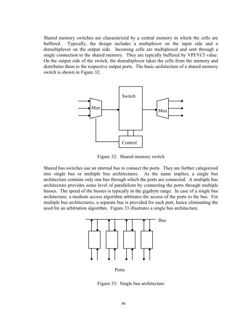
Shared memory switches are characterized by a central memory in which the cells are<br />
buffered. Typically, the design includes a multiplexor on the input side and a<br />
demultiplexor on the output side. Incoming cells are multiplexed and sent through a<br />
single connection to the shared memory. They are typically buffered by VPI/VCI value.<br />
On the output side of the switch, the demultiplexor takes the cells from the memory and<br />
distributes them to the respective output ports. The basic architecture of a shared memory<br />
switch is shown in Figure 32.<br />
Switch<br />
Mux<br />
Mux<br />
Control<br />
Figure 32: Shared memory switch<br />
Shared bus switches use an internal bus to connect the ports. They are further categorized<br />
into single bus or multiple bus architectures. As the name implies, a single bus<br />
architecture contains only one bus through which the ports are connected. A multiple bus<br />
architecture provides some level of parallelism by connecting the ports through multiple<br />
busses. The speed of the busses is typically in the gigabyte range. In case of a single bus<br />
architecture, a medium access algorithm arbitrates the access of the ports to the bus. For<br />
multiple bus architectures, a separate bus is provided for each port, hence eliminating the<br />
need for an arbitration algorithm. Figure 33 illustrates a single bus architecture.<br />
Bus<br />
Ports<br />
Figure 33: Single bus architecture<br />
86