184-Pin Unbuffered Double Data Rate SDRAM UDIMM DDR SDRAM
184-Pin Unbuffered Double Data Rate SDRAM UDIMM DDR SDRAM
184-Pin Unbuffered Double Data Rate SDRAM UDIMM DDR SDRAM

You also want an ePaper? Increase the reach of your titles
YUMPU automatically turns print PDFs into web optimized ePapers that Google loves.
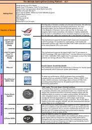
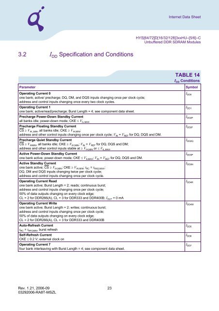
3.2 I DD Specification and Conditions<br />
Rev. 1.21, 2006-09 23<br />
03292006-RA8T-MSZL<br />
Internet <strong>Data</strong> Sheet<br />
HYS[64/72]D[16/32/128]3xxHU–[5/6]–C<br />
<strong>Unbuffered</strong> <strong>DDR</strong> <strong>SDRAM</strong> Modules<br />
TABLE 14<br />
I DD Conditions<br />
Parameter Symbol<br />
Operating Current 0<br />
one bank; active/ precharge; DQ, DM, and DQS inputs changing once per clock cycle;<br />
address and control inputs changing once every two clock cycles.<br />
Operating Current 1<br />
one bank; active/read/precharge; Burst Length = 4; see component data sheet.<br />
Precharge Power-Down Standby Current<br />
all banks idle; power-down mode; CKE � V IL,MAX<br />
Precharge Floating Standby Current<br />
CS � VIH,,MIN, all banks idle; CKE � VIH,MIN; address and other control inputs changing once per clock cycle; VIN = VREF for DQ, DQS and DM.<br />
Precharge Quiet Standby Current<br />
CS � VIHMIN , all banks idle; CKE � VIH,MIN ; VIN = VREF for DQ, DQS and DM;<br />
address and other control inputs stable at � VIH,MIN or � VIL,MAX .<br />
Active Power-Down Standby Current<br />
one bank active; power-down mode; CKE � V ILMAX ; V IN = V REF for DQ, DQS and DM.<br />
Active Standby Current<br />
one bank active; CS � V IH,MIN; CKE � V IH,MIN; t RC = t RAS,MAX;<br />
DQ, DM and DQS inputs changing twice per clock cycle;<br />
address and control inputs changing once per clock cycle.<br />
Operating Current Read<br />
one bank active; Burst Length = 2; reads; continuous burst;<br />
address and control inputs changing once per clock cycle;<br />
50% of data outputs changing on every clock edge;<br />
CL = 2 for <strong>DDR</strong>266(A), CL = 3 for <strong>DDR</strong>333 and <strong>DDR</strong>400B; I OUT =0mA<br />
Operating Current Write<br />
one bank active; Burst Length = 2; writes; continuous burst;<br />
address and control inputs changing once per clock cycle;<br />
50% of data outputs changing on every clock edge;<br />
CL = 2 for <strong>DDR</strong>266(A), CL = 3 for <strong>DDR</strong>333 and <strong>DDR</strong>400B<br />
Auto-Refresh Current<br />
tRC = tRFCMIN, burst refresh<br />
Self-Refresh Current<br />
CKE � 0.2 V; external clock on<br />
Operating Current 7<br />
four bank interleaving with Burst Length = 4; see component data sheet.<br />
I DD0<br />
I DD1<br />
I DD2P<br />
I DD2F<br />
I DD2Q<br />
I DD3P<br />
I DD3N<br />
I DD4R<br />
I DD4W<br />
I DD5<br />
I DD6<br />
I DD7