184-Pin Unbuffered Double Data Rate SDRAM UDIMM DDR SDRAM
184-Pin Unbuffered Double Data Rate SDRAM UDIMM DDR SDRAM
184-Pin Unbuffered Double Data Rate SDRAM UDIMM DDR SDRAM

You also want an ePaper? Increase the reach of your titles
YUMPU automatically turns print PDFs into web optimized ePapers that Google loves.
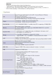
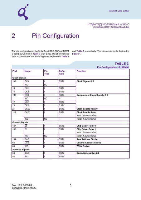
2 <strong>Pin</strong> Configuration<br />
The pin configuration of the <strong>Unbuffered</strong> <strong>DDR</strong> <strong>SDRAM</strong> DIMM<br />
is listed by function in Table 3 (<strong>184</strong> pins). The abbreviations<br />
used in columns <strong>Pin</strong> and Buffer Type are explained in Table 4<br />
<strong>Pin</strong># Name <strong>Pin</strong><br />
Type<br />
Buffer<br />
Type<br />
Rev. 1.21, 2006-09 5<br />
03292006-RA8T-MSZL<br />
Internet <strong>Data</strong> Sheet<br />
HYS[64/72]D[16/32/128]3xxHU–[5/6]–C<br />
<strong>Unbuffered</strong> <strong>DDR</strong> <strong>SDRAM</strong> Modules<br />
and Table 5 respectively. The pin numbering is depicted in<br />
Figure 1.<br />
Function<br />
Clock Signals<br />
137 CK0 I SSTL Clock Signals 2:0<br />
NC NC –<br />
16 CK1 I SSTL<br />
76 CK2 I SSTL<br />
138 CK0 I SSTL Complement Clock Signals 2:0<br />
NC NC –<br />
17 CK1 I SSTL<br />
75 CK2 I SSTL<br />
21 CKE0 I SSTL Clock Enable Rank 0<br />
111 CKE1 I SSTL Clock Enable Rank 1<br />
Note: 2-rank module<br />
NC NC – Note: 1-rank module<br />
Control Signals<br />
157 S0 I SSTL Chip Select Rank 0<br />
158 S1 I SSTL Chip Select Rank 1<br />
Note: 2-rank module<br />
NC NC – Note: 1-rank module<br />
154 RAS I SSTL Row Address Strobe<br />
65 CAS I SSTL Column Address Strobe<br />
63 WE I SSTL Write Enable<br />
Address Signals<br />
59 BA0 I SSTL Bank Address Bus 2:0<br />
52 BA1 I SSTL<br />
TABLE 3<br />
<strong>Pin</strong> Configuration of <strong>UDIMM</strong>